Embed Size (px)
Citation preview
CHAPTER 1
INTRODUCTION
1.1 Introduction
Power dissipation is recognized as a critical parameter in modern VLSI design
field. To satisfy MOORE’S law and to produce consumer electronics goods with
more backup and less weight, low power VLSI design is necessary.
Fast Multiplier and Accumulators are essential parts of digital signal
processing systems. MAC is the unit which combines an Adder and Multiplier. This
will give the summation of multiplication products. In both of these Operations
Multiplication takes more cycles than Accumulation. The speed of multiply operation
is of great importance in digital signal processing as well as in the general purpose
processors today, especially since the media processing took off. In the past
multiplication was generally implemented via a sequence of addition, subtraction, and
shift operations. Multiplication can be considered as a series of repeated additions.
The number to be added is the multiplicand, the number of times that it is added is the
multiplier, and the result is the product. Each step of addition generates a partial
product. In most computers, the operand usually contains the same number of bits.
When the operands are interpreted as integers, the product is generally twice the
length of operands in order to preserve the information content. This repeated addition
method that is suggested by the arithmetic definition is slow that it is almost always
replaced by an algorithm that makes use of positional representation. It is possible to
decompose multipliers into two parts. The first part is dedicated to the generation of
partial products, and the second one collects and adds them.
The basic multiplication principle is twofold i.e. evaluation of partial products
and accumulation of the shifted partial products. It is performed by the successive
additions of the columns of the shifted partial product matrix. The ‘multiplier’ is
successfully shifted and gates the appropriate bit of the ‘multiplicand’. The delayed,
gated instance of the multiplicand must all be in the same column of the shifted partial
product matrix. They are then added to form the product bit for the particular form.
Multiplication is therefore a multi operand operation. To extend the multiplication to
1

both signed and unsigned numbers, a convenient number system would be the
representation of numbers in two’s complement format.
The MAC (Multiplier and Accumulator Unit) is used for image processing and
digital signal processing (DSP) in a DSP processor. Algorithm of MAC is Booth's
radix-4 algorithm, Modified Booth Multiplier; 17-bit SPST adder improves speed and
reduces the power.
1.2 Background of Multiplier And Accumulator(MAC) unit
In computing, especially digital signal processing, multiply-accumulate is a
common operation that computes the product of two numbers and adds that product to
an accumulator. When done with floating point numbers it might be performed with
two rounding (typical in many DSPs) or with a single rounding. When performed
with a single rounding, it is called a fused multiply-add (FMA) or fused multiply-
accumulate (FMAC).
Modern computers may contain a dedicated multiply-accumulate unit, or
"MAC unit", consisting of a multiplier implemented in combinational logic followed
by an adder and an accumulator register which stores the result when clocked. The
output of the register is fed back to one input of the adder, so that on each clock the
output of the multiplier is added to the register. Combinational multipliers require a
large amount of logic, but can compute a product much more quickly than the method
of shifting and adding typical of earlier computers. The first processors to be equipped
with MAC-units were digital signal processors, but the technique is now common in
general-purpose processors too.
A conventional MAC unit consists of (fast multiplier) booth multiplier and an
accumulator that contains the signed or unsigned extended sum of the previous
consecutive products.
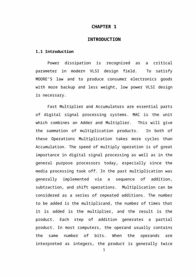
As shown in Figure 1.1, the multiplier and the adder are the combination
circuits. The multiplier shown was the booth multiplier whereby the adder was the
accumulator. From Equation 1.1.
F = Σ Xi Yi………………………………. eq 1.1
2

Xi and Yi are either the unsigned or signed data inputs. ‘N’ is the number of
partialproducts accumulated by the MAC unit. Two different values X and Y (in same
bits length) are multiplied each other using booth multiplier and the multiplication
result will be fed into the accumulator. At the same time, the accumulator will add up
the booth multiplier output and the output of the accumulator register. Initially,
during the first clock cycle, the output of register will be reset to have a zero values
output.
Figure 1.1 Block diagram of MAC
After the first time output of the accumulator is loaded into the register.
Meanwhile the third clock cycle time will let the accumulator to add up the output of
the booth multiplier with output of the register.
In conjunction with the objective of this project, the MAC unit is emphasized
in improving the design speed and lowering the design power consumption. The first
one is the partial products reduction network and the second one is the accumulator
since both of these stages require addition of large operands that involves long paths
for carry propagation.
1.3 Objective
The main objective of this thesis is to design and implementation of a
Multiplier and Accumulator. A multiplier which is a combination of Modified Booth
and SPST (Spurious Power Suppression Technique) adder are designed taking into
account the less area consumption of booth algorithm because of less number of
3
partial products and more speedy accumulation of partial products and less power
consumption of partial products addition using SPST adder approach.
To increase the MAC unit design speed by using the Booth Multiplier,
To decrease the power consumption by using SPST adder.
1.4 Methodology
This paper proposes a new architecture of multiplier-and-accumulator (MAC)
for high speed and low-power by adopting the new SPST implementing approach.
This multiplier is designed by equipping the Spurious Power Suppression Technique
(SPST) on a modified Booth encoder which is controlled by a detection unit using an
AND gate. The modified booth encoder will reduce the number of partial products
generated by a factor of 2. The SPST adder will avoid the unwanted addition and thus
minimize the switching power dissipation. By combining multiplication with
accumulation and devising a low power equipped SPST, the performance was
improved.
In this project we used Xilinx-ISE Simulator for logical verification, and
further synthesizing it on Xilinx-XST tool using target technology and performing
placing & routing operation for system verification on targeted FPGA.
1.5 Significance of this work
Digital Signal processing (DSP) is used in a wide range of application such as
speech and audio coding, image processing and video, pattern recognition and so on.
In real time Very Large Scale Integration (VLSI) implementation of the DSP
instruction, the system requires hardware architecture which can process input signal
samples as they received. Most of the DSP computation involves the use of multiply
and multiply accumulate operations and therefore Multiplier Accumulator (MAC)
unit is very important in DSP application. In Cryptography implementations We need
a more speed MAC unit. As Our designed MAC unit is the optimized design for both
power and speed it is better to use in both of the applications.
The multiplication circuit represents the core of the MAC unit. Most of the
effort focused on improving the performance of digital multiplication has been
4

focusing on increasing the speed of operation and decreasing the power consumption.
In this project, modified booth encoder is used to increase the speed of operation and
SPST approach is used to decrease the power consumed by the MAC unit.
1.6 Applications
Multimedia and communication systems
Real-time signal processing like Audio signal processing, video/image processing, or
large-capacity data processing
Cryptography Algorithm implementations such as Computations in Security
Algorithms.
1.7 Outline of this report
This report is divided into 5 chapters. The following chapter (Chapter 2) is regarding
the literature review of the MAC unit design. Chapter 3 explained the MAC unit
design methodologies whereas chapter 4 covers the FPGA ,XILINX and Verilog
Introduction, chapter 5 contains results and discussion on all the waveforms and
power consumption, design speed, area analysis result. Finally, in the last chapter
which is Chapter 6 summarizes the results and comes to the conclusions from this
final year project work. Moreover, some suggestions on the future possible
improvements are discussed in this chapter.
1.8 Conclusion
This chapter had outlined the overview, the status of problems, the objectives
and also the project methodology of this project. It also had introduced the
background of the multiplier accumulator and booth multiplier. All the design
functionality on how it works had been explained clearly in this chapter. Lastly, these
chapters also cover the overview on next others chapter’s contents.
1.9 Software used
Language used: VHDL
XILINX 10.1—Simulation
5

XILINX 10.1 –synthesis and implementation
1.10 Hardware used
Spartan3 FPGA Kit –For implementation
6

CHAPTER 2
LITERATURE REVIEW
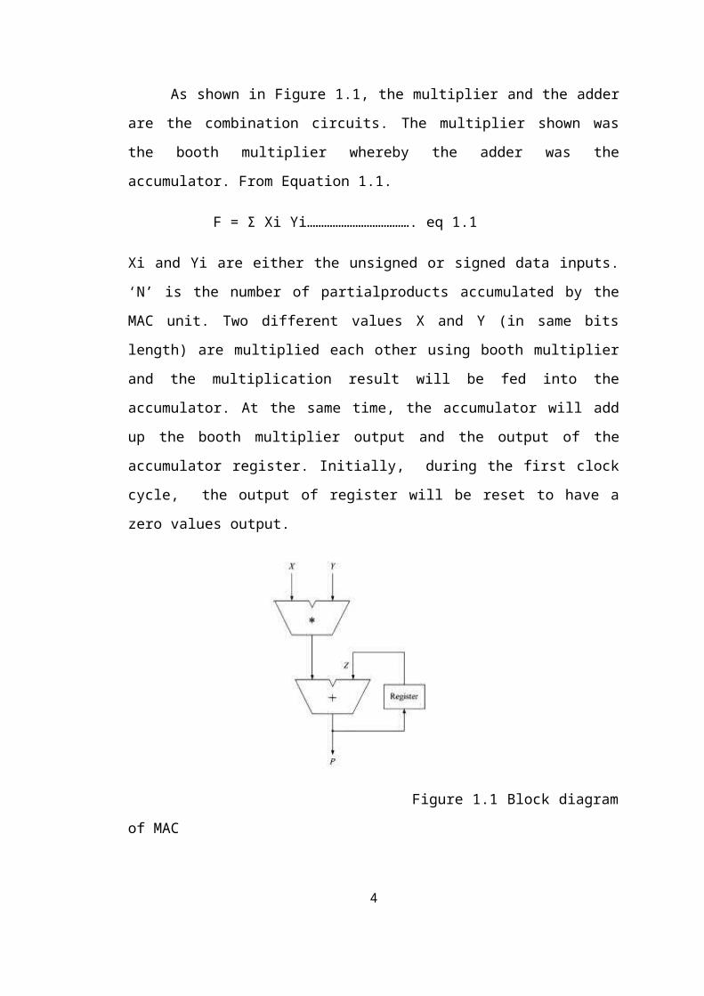
2.1 Background of MAC
In the majority of digital signal processing (DSP) applications the critical
operations are the multiplication and accumulation, especially digital signal
processing, multiply-accumulate is a common operation that computes the product of
two numbers and adds that product to an accumulator. When done with floating point
numbers it might be performed with two rounding (typical in many DSPs) or with a
single rounding. When performed with a single rounding, it is called a fused multiply-
add (FMA) or fused multiply-accumulate (FMAC).
Figure 2.1 MAC Architecture with Radix 4 Booth Multiplier
Real-time signal processing requires high speed and high throughput Multiplier-
Accumulator (MAC) unit that consumes low power, which is always a key to achieve
a high performance digital signal processing system. The purpose of this work is to
design and implementation of a low power MAC unit with block enabling technique
to save power.
7

2.2 Basics of Multiplier
Multiplication is a mathematical operation that at its simplest is an abbreviated
process of adding an integer to itself a specified number of times. A number
(multiplicand) is added to itself a number of times as specified by another number
(multiplier) to form a result (product). In elementary school, students learn to
multiply by placing the multiplicand on top of the multiplier. The multiplicand is then
multiplied by each digit of the multiplier beginning with the rightmost, Least
Significant Digit (LSD). Intermediate results (partial products) are placed one atop
the other, offset by one digit to align digits of the same weight. The final product is
determined by summation of all the partial-products. Although most people think of
multiplication only in base 10, this technique applies equally to any base, including
binary. Figure 2.1 shows the data flow for the basic multiplication technique just
described. Each black dot represents a single digit.
Figure 2.2 Basic Multiplication
Here, we assume that MSB represent the sign of the digit. The operation of
multiplication is rather simple in digital electronics. It has its origin from the classical
algorithm for the product of two binary numbers. This algorithm uses addition and
shift left operations to calculate the product of two numbers. Based upon the above
procedure, we can deduce an algorithm for any kind of multiplication which is shown
in figure 2.2. We can check at the initial stage also that whether the product will be
positive or negative or after getting the whole result, MSB of the results tells the sign
of the product.
8

Figure 2.3 Signed Multiplication Algorithm
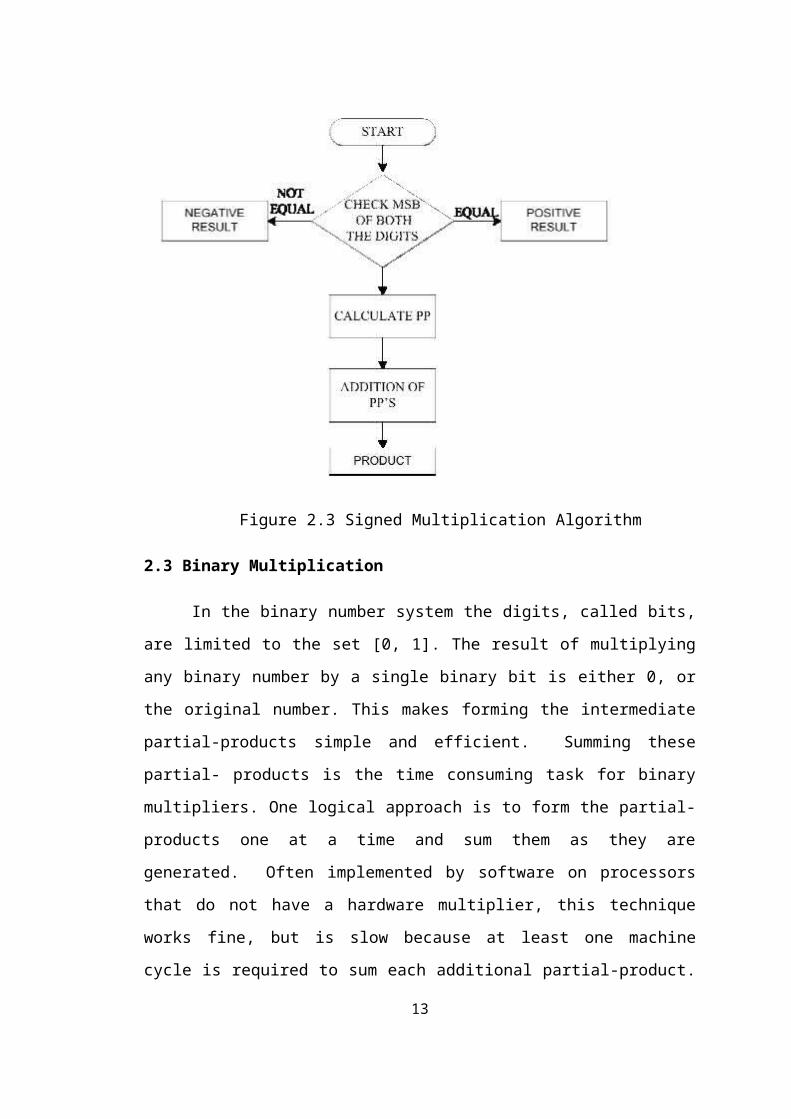
2.3 Binary Multiplication
In the binary number system the digits, called bits, are limited to the set [0, 1].
The result of multiplying any binary number by a single binary bit is either 0, or the
original number. This makes forming the intermediate partial-products simple and
efficient. Summing these partial- products is the time consuming task for binary
multipliers. One logical approach is to form the partial-products one at a time and sum
them as they are generated. Often implemented by software on processors that do not
have a hardware multiplier, this technique works fine, but is slow because at least one
machine cycle is required to sum each additional partial-product. For applications
where this approach does not provide enough performance, multipliers can be
implemented directly in hardware. The two main categories of binary multiplication
include signed and unsigned numbers. Digit multiplication is a series of bit shifts and
series of bit additions, where the two numbers, the multiplicand and the multiplier
are combined into the result. Considering the bit representation of the multiplicand x
= xn-1…..x1 x0 and the multiplier y = yn-1…..y1y0 in order to form the product up to
n shifted copies of the multiplicand are to be added for unsigned multiplication. The
9
entire process consists of three steps, partial product generation, partial product
reduction and final addition.
2.4 Multiplication process
The simplest multiplication operation is to directly calculate the product of
two numbers by hand. This procedure can be divided into three steps: partial product
generation, partial product reduction and the final addition. To further specify the
operation process, let us calculate the product of 2 two’s complement numbers, for
example, 11012 (−310) and 01012 (510), when computing the product by hand, which
can be described according to figure 2.3.
Figure 2.4 Multiplication calculations by hand
The bold italic digits are the sign extension bits of the partial products. The first
operand is called the multiplicand and the second the multiplier. The intermediate
products are called partial products and the final result is called the product. However,
the multiplication process, when this method is directly mapped to hardware, is shown
in figure 2.4. As can been seen in the figures, the multiplication operation in hardware
consists of PP generation, PP reduction and final addition steps. The two rows before
the product are called sum and carry bits. The operation of this method is to take one
of the multiplier bits at a time from right to left, multiplying the multiplicand by the
single bit of the multiplier and shifting the intermediate product one position to the
left of the earlier intermediate products. All the bits of the partial products in each
10

column are added to obtain two bits: sum and carry. Finally, the sum and carry bits in
each column have to be summed. Similarly, for the multiplication of an n-bit
multiplicand and an m-bit multiplier, a product with n + m bits long and m partial
products can be generated. The method shown in figure 1.3 is also called a non-Booth
encoding scheme.
Figure 2.5 Multiplication Operation in hardware
2.5 Modified Booth Encoder
2.5.1 Booth’s Multplication Algorithm
It is a multiplication algorithm that multiplies two signed binary numbers in
two's complement notation. The algorithm was invented by Andrew Donald Booth
in 1951. Which Algorithm is faster than the normal Multiplication Algorithm by
using a shifting operation instead of addition operation. Booth algorithm is widely
used in the implementations of hardware or software multipliers because its
application makes it possible to reduce the number of partial products. It can be used
for both sign magnitude numbers as well as 2’s complement numbers.
11

Procedure
Booth's algorithm involves repeatedly adding one of two predetermined values
A and S to a product P where A and S are Addition and Subtraction , then performing
a rightward arithmetic shift on P . Let m and r be the multiplicand and multiplier,
respectively; and let x and y represent the number of bits in m and r.
I. Determine the values of A and S , and the initial value of P . All of these numbers
should have a length equal to ( + x y+1)
1. A: Fill the most significant (leftmost) bits with the value of m . Fill the remaining (
+ 1) y bits with zeros.
2. S: Fill the most significant bits with the value of (− ) in two's complement notation.
Fill the remaining ( + 1) bits with zeros. the least significant (rightmost) bit with a
zero.
3. 3. P: Fill the most significant x bits with zeros. To the right of this, append the
value of .
II. Determine the two least significant (rightmost) bits of P
If they are 01, find the value of P + A . Ignore any overflow.
If they are 10, find the value of P + S. Ignore any overflow.
If they are 00, do nothing. Use P directly in the next step.
If they are 11, do nothing. Use P directly in the next step.
Arithmetically shift the value obtained in the 2nd step by a single place to the right.
Let P now equal this new value.
Repeat steps 2 and 3 until they have been done y times.
Drop the least significant (rightmost) bit from P . T his is the product of m and r
Example
12
Find 3 × (−4), with m = 3 and r = −4, and x = 4 and y = 4:
A = 0011 0000 0
P = 0000 1100 0
S = 1101 0000 0
Perform the loop four times :
P = 0000 11000. T he last two bits are 00.
P = 0000 0110 0. Arithmetic right shift.
P = 0000 01100. The last two bits are 00.
P = 0000 0011 0. Arithmetic right shift.
P = 0000 0010. The last two bits are 10.
P = 1101 0011 0. P = P + S.
P = 1110 1001 1. Arithmetic right shift.
P = 1110 10011. The last two bits are 11.
P = 1111 0100 1. Arithmetic right shift.
The product is 1111 0100, which is −12.
In which algorithm the total number of computations are of no of multiplier
bits. This technique is inadequate when multiplicand is the largest negative number
for example if the multiplicand has 4 bits then this value is -8.
For the better utilization of algorithm we have to multiplicand and multiplier
before operation starts, since XY and YX are the same. As per the algorithm for the
pair of Product 00 and 11 we have to perform only one Arithmetic Right Shift
operation, whereas for 01 we need to perform an addition operation also along with
the shifting operation. likewise for 10 we need to perform a subtraction i.e addition of
S operation also alongside the normal shifting operation, which leads some extra
computations so it is better to choose the value having large rail of 1’s or a number
13

having less number of 01 and 10 pairs as a multiplier and the another one as the
multiplicand. For example if we need to multiply 1110 and 1010 we have to choose
first one as multiplier and the second one as multiplicand.
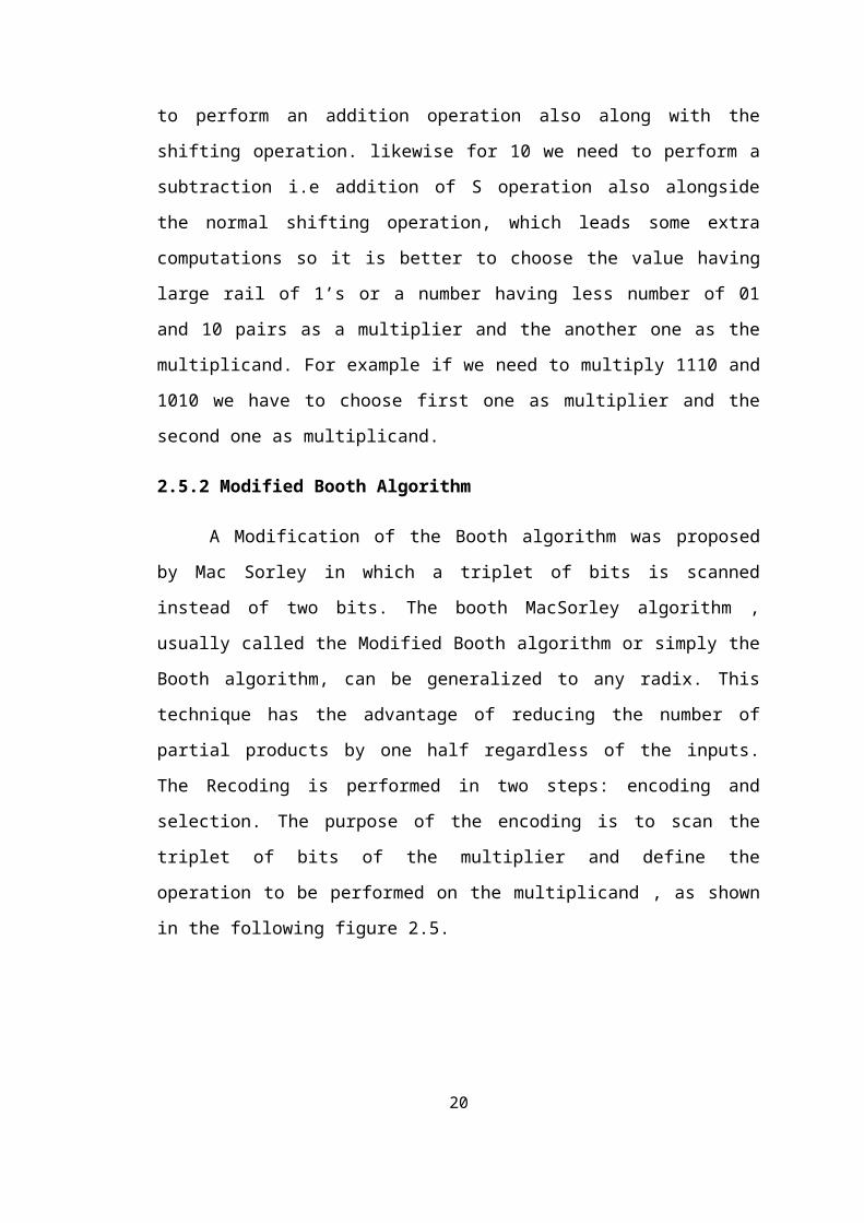
2.5.2 Modified Booth Algorithm
A Modification of the Booth algorithm was proposed by Mac Sorley in which
a triplet of bits is scanned instead of two bits. The booth MacSorley algorithm ,
usually called the Modified Booth algorithm or simply the Booth algorithm, can be
generalized to any radix. This technique has the advantage of reducing the number of
partial products by one half regardless of the inputs. The Recoding is performed in
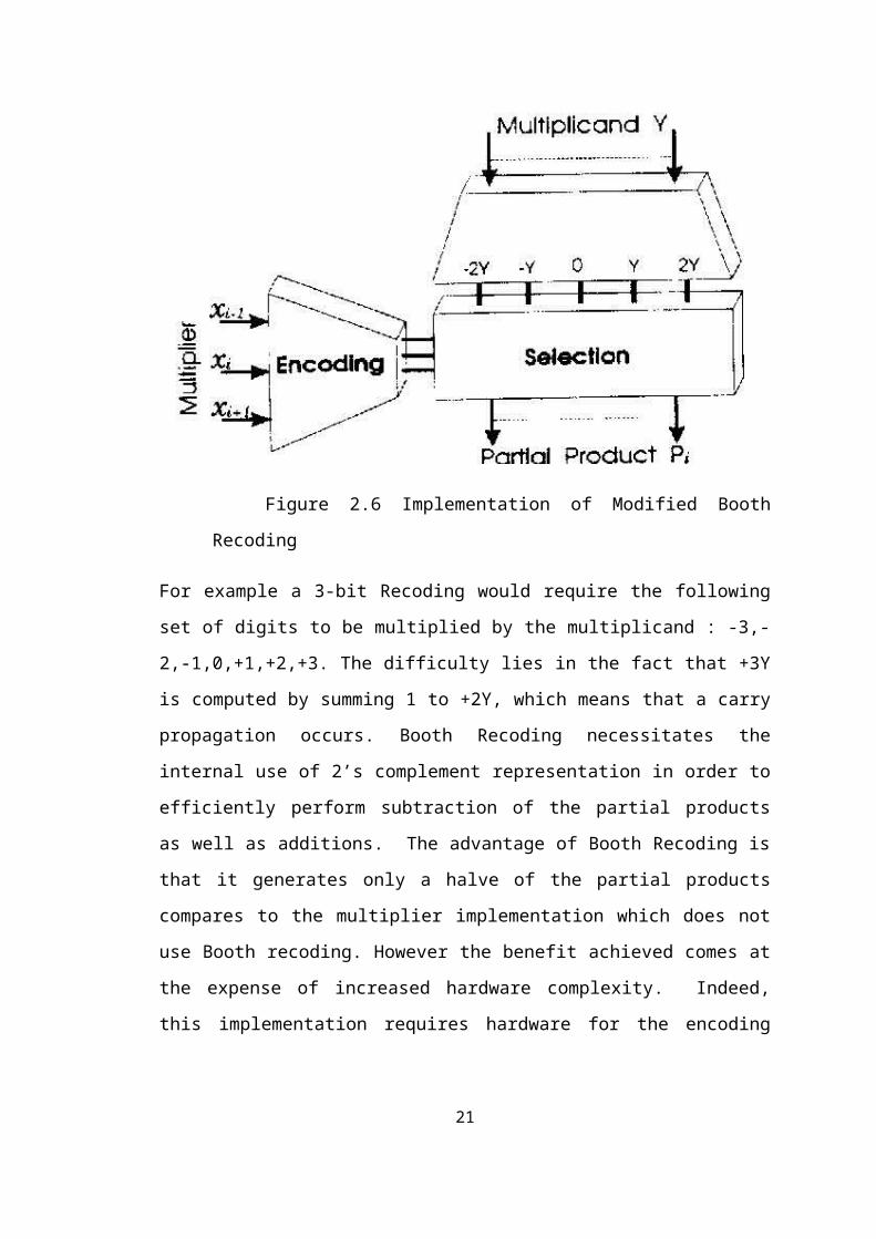
two steps: encoding and selection. The purpose of the encoding is to scan the triplet of
bits of the multiplier and define the operation to be performed on the multiplicand , as
shown in the following figure 2.5.
Figure 2.6 Implementation of Modified Booth Recoding
For example a 3-bit Recoding would require the following set of digits to be
multiplied by the multiplicand : -3,-2,-1,0,+1,+2,+3. The difficulty lies in the fact that
+3Y is computed by summing 1 to +2Y, which means that a carry propagation
occurs. Booth Recoding necessitates the internal use of 2’s complement
representation in order to efficiently perform subtraction of the partial products as
14

well as additions. The advantage of Booth Recoding is that it generates only a halve
of the partial products compares to the multiplier implementation which does not use
Booth recoding. However the benefit achieved comes at the expense of increased
hardware complexity. Indeed, this implementation requires hardware for the
encoding and for the selection of the partial products(-2Y,-Y,0,+Y,+2Y).
Figure 2.7 System Architecture for Multiplier With Radix4 MBA
2.6 Overview of MAC
A multiplier can be divided into three operational steps. The first is radix-2
Booth encoding in which a partial product is generated from the multiplicand X and
the multiplier Y. The second is adder array or partial product compression to add all
partial products. The last is the final addition in which the process to accumulate the
multiplied results is included. The general hardware architecture of this MAC is
shown in Fig.1.2. It executes the multiplication operation by multiplying the input
multiplier X and the multiplicand Y. This is added to the previous multiplication
result Z as the accumulation step. The N-bit 2’s complement binary number can be
expressed as
……..(2.1)15

If (2.1) is expressed in base-4 type redundant sign digit form in order to apply the
radix-2 Booth’s algorithm.
……………………….………...………....(2.2)
…..…..……………….…(2.3)
If (2.2) is used, multiplication can be expressed as
……………..………………….(2.4)
If these equations are used, the afore-mentioned multiplication–accumulation results
can be expressed as
…………(2.5)
Each of the two terms on the right-hand side of (2.5) is calculated
independently and the final result is produced by adding the two results. The MAC
architecture implemented by (2.5) is called the standard design. If N-bit data are
multiplied, the number of the generated partial products is proportional to N. In
order to add them serially, the execution time is also proportional to N. The
architecture of a multiplier, which is the fastest, uses radix-2 Booth encoding that
generates partial products. If radix-2 Booth encoding is used, the number of partial
products, is reduced to half, resulting in the decrease in Addition of Partial Products
step. In addition, the signed multiplication based on 2’s complement numbers is also
possible. Due to these reasons, most current used multipliers adopt the Booth
encoding.
16
2.7 Existing MAC Architecture
MAC is composed of an adder, multiplier and an accumulator. Usually adders
implemented are Carry- Select or Carry-Save adders, as speed is of utmost importance
in DSP (Chandrakasan, Sheng, & Brodersen, 1992 and Weste & Harris, 3rd Ed). One
implementation of the multiplier could be as a parallel array multiplier. The inputs for
the MAC are to be fetched from memory location and fed to the multiplier block of
the MAC, which will perform multiplication and give the result to adder which will
accumulate the result and then will store the result into a memory location. This entire
process is to be achieved in a single clock cycle (Weste & Harris, 3rd Ed). The
architecture of the MAC unit which had been designed in this work consists of one 16
bit register, one 16-bit Modified Booth Multiplier, 32-bit accumulator. To multiply
the values of A and B, Modified Booth multiplier is used instead of conventional
multiplier because Modified Booth multiplier can increase the MAC unit design speed
and reduce multiplication complexity. SPST Adder is used for the addition of partial
products and a register is used for accumulation. The operation of the designed MAC
unit is as in Equation 1.1. The product of Ai X Bi is always fed back into the 32-bit
accumulator and then added again with the next product Ai x Bi. This MAC unit is
capable of multiplying and adding with previous product consecutively up to as many
as times.
17
CHAPTER 3
DESIGN OF MAC
The digital signal processing such as filtering, convolution, and inner
products. Most digital signal processing methods use nonlinear functions such as
discrete cosine transform (DCT) [2] or discrete wavelet transform (DWT) [3].
Because they are basically accomplished by repetitive application of multiplication
and addition, the speed of the multiplication and addition arithmetic determines the
execution speed and performance of the entire calculation. Because the multiplier
requires the longest delay among the basic operational blocks in digital system, the
critical path is determined by the multiplier, in general. For high-speed multiplication,
the modified radix-4 Booth’s algorithm (MBA) [4] is commonly used. However, this
cannot completely solve the problem due to the long critical path for multiplication
[5], [6]. In general, a multiplier uses Booth’s algorithm [7] and array of full adders
(FAs), or Wallace tree [8] instead of the array of FAs., i.e., this multiplier mainly
consists of the three parts: Booth encoder, a tree to compress the partial products such
as Wallace tree, and final adder [9], [10]. Because Wallace tree is to add the partial
products from encoder as parallel as possible, its operation time is proportional to ,
where is the number of inputs. It uses the fact that counting the number of 1’s among
the inputs reduces the number of outputs into.
In real implementation, many (3:2) or (7:3) counters are used to reduce the
number of outputs in each pipeline step. The most effective way to increase the speed
of a multiplier is to reduce the number of the partial products because multiplication
proceeds a series of additions for the partial products. To reduce the number of
calculation steps for the partial products, MBA algorithm has been applied mostly
whereWallace tree has taken the role of increasing the speed to add the partial
products. To increase the speed of the MBA algorithm, many parallel multiplication
architectures have been researched [11]–[13]. Among them, the architectures based on
the Baugh–Wooley algorithm (BWA) have been developed and they have been
applied to various digital filtering calculations [14]–[16]. One of the most advanced
types of MAC for general-purpose digital signal processing has been proposed by
Elguibaly [17]. It is an architecture in which accumulation has been combined with
18

the carry save adder (CSA) tree that compresses partial products. In the architecture
proposed in [17], the critical path was reduced by eliminating the adder for
accumulation and decreasing the number of input bits in the final adder. While it has a
better performance because of the reduced critical path compared to the previous
MAC architectures, there is a need to improve the output rate due to the use of the
final adder results for accumulation.
Architecture to merge the adder block to the accumulator register in the MAC
operator was proposed in [18] to provide the possibility of using two separate /2-bit
adders instead of one -bit adder to accumulate the –bitMAC results. Recently, Zicari
proposed an architecture that took a merging technique to fully utilize the
Figure 3.1 Basic arithmetic steps of multiplication and accumulation.
Also took this compressor as the basic building blocks for the multiplication circuit.
In this paper, a new architecture for a high-speed MAC is proposed. In this MAC, the
computations of multiplication and accumulation are combined and a hybrid-type
CSA structure is proposed to reduce the critical path and improve the output rate. It
19
uses MBA algorithm based on 1’s complement number system. A modified array
structure for the sign bits is used to increase the density of the operands. A carry look-
ahead adder (CLA) is inserted in the CSA tree to reduce the number of bits in the final
adder. In addition, in order to increase the output rate by optimizing the pipeline
efficiency, intermediate calculation results are accumulated in the form of sum and
carry instead of the final adder outputs.This paper is organized as follows. In Section
II, a simple introduction of a general MAC will be given, and the architecture for the
proposed MAC will be described in Section III. In Section IV, the implementation
result will be analyzed and the characteristic of the proposed MAC will be shown.
3.1 Overview of MAC
Figure 3.2 Hardware architecture of general MAC
In this section, basic MAC operation is introduced. A multiplier can be divided into
three operational steps. The first is radix-2 Booth encoding in which a partial product
is generated from the multiplicand and the multiplier .The second is adder array or
partial product compression to add all partial products and convert them into the form
of sum and carry. The last is the final addition in which the final multiplication result
is produced by adding the sum and the carry. If the process to accumulate the
multiplied results is included, a MAC consists of four steps, as shown in Fig. 1, which
shows the operational steps explicitly. A general hardware architecture of this MAC is
shown in Fig. 2. It executes the multiplication operation by multiplying the input
20
multiplier and the multiplicand . This is added to the previous multiplication result as
the accumulation step.
Each of the two terms on the right-hand side of (5) is calculated independently and the
final result is produced by adding the two results. The MAC architecture implemented
by (5) is called the standard design [6]. If -bit data are multiplied, the number of the
generated partial products is proportional to . In order to add them serially, the
execution time is also proportional to . The architecture of a multiplier, which is the
fastest, uses radix-2 Booth encoding that generates partial products and aWallace tree
based on CSA as the adder array to add the partial products. If radix-2 Booth
encoding is used, the number of partial products, i.e., the inputs to the Wallace tree, is
reduced to half, resulting in the decrease in CSA tree step. In addition, the signed
multiplication based on 2’s complement numbers is also possible. Due to these
reasons, most current used multipliers adopt the Booth encoding.
3.2 Proposed MAC Architecture
In this section, the expression for the new arithmetic will be derived from
equations of the standard design. a hybrid-typed CSA architecture that can satisfy the
operation of the proposed MAC will be proposed. A. If an operation to multiply two –
21
bit numbers and accumulate into a 2 -bit number is considered, the critical path is
determined by the 2 -bit accumulation operation.
The delay of the last accumulator must be reduced in order to improve the
performance of the MAC. The overall performance of the proposed MAC is improved
by eliminating the accumulator itself by combining it with the CSA function. If the
accumulator has been eliminated, the critical path is then determined by the final
adder in the multiplier. The basic method to improve the performance of the final
adder is to decrease the number of input bits. In order to reduce this number of input
bits, the multiple partial products are compressed into a sum and a carry by CSA. The
number of bits of sums and carries to be transferred to the final adder is reduced by
adding the lower bits of sums and carries in advance within the range in which the
overall performance will not be degraded. A 2-bit CLA is used to add the lower bits in
the CSA. In addition, to increase the output rate when pipelining is applied, the sums
and carrys from the CSA are accumulated instead of the outputs from the final adder
in the manner that the sum and carry from the CSA in the previous cycle are inputted
to CSA. Due to this feedback of both sum and carry, the number of inputs to CSA
increases, compared to the standard design and [17]. In order to efficiently solve the
increase in the amount of data, a CSA architecture is modified to treat the sign bit.
Figure 3.3 Hardware architecture of the proposed MAC.
22

Figure 3.4 Proposed arithmetic operation of multiplication and accumulation.
If the MAC process proposed in the previous section is rearranged, it would be
as Fig. 3.4, in which the MAC is organized into three steps. When compared with Fig.
1, it is easy to identify the difference that the accumulation has been merged into the
process of adding the partial products. Another big difference from Fig. 1 is that the
final addition process in step 3 is not always run even though it does not appear
explicitly in Fig. 3. Since accumulation is carried out using the result from step 2
instead of that from step 3, step 3 does not have to be run until the point at which the
result for the final accumulation is needed. The hardware architecture of the MAC to
satisfy the process in Fig. 3 is shown in Fig. 4. The -bitMAC inputs, and , are
converted into an -bit partial product by passing through the Booth encoder. In the
CSA and accumulator, accumulation is carried out along with the addition of the
partial products. As a result, -bit , and (the result from adding the lower bits of the
sum and carry) are generated. These three values are fed back and used for the next
accumulation. If the final result for the MAC is needed, is generated by adding and in
the final adder and combined with that was already generated.
23

The architecture of the hybrid-type CSA that complies with the operation of
the proposed MAC is shown in Fig. 5, which performs 8 8-bit operation. It was
formed based on (12). In Fig. 5, is to simplify the sign expansion and is to compensate
1’s complement number into 2’s complement number. and correspond to the th bit of
the feedback sum and carry. is the th bit of the sum of the lower bits for each partial
product that were added in advance and is the previous result. In addition,
corresponds to the th bit of the th partial product. Since the multiplier is for 8 bits,
totally four partial products are generated from the Booth encoder. In (11), and
correspond to and , respectively. This CSA requires at least four rows of FAs for the
four partial products. Thus, totally five FA rows are necessary since one more level of
rows are needed for accumulation. For an -bit MAC operation, the level of CSA is .
The white square in Fig. 5 represents an FA and the gray square is a half adder (HA).
The rectangular symbol with five inputs is a 2-bit CLA with a carry input.
The critical path in this CSA is determined by the 2-bit CLA. It is also
possible to use FAs to implement the CSA without CLA. However, if the lower bits
of the previously generated partial product are not processed in advance by the CLAs,
the number of bits for the final adder will increase. When the entire multiplier or
MAC is considered, it degrades the performance. In Table I, the characteristics of the
proposed CSA architecture have been summarized and briefly compared with other
architectures.
24

Figure 3.5 Proposed CSA Architecture
Table 3.1 Gate size of logic circuit element
25
Table 3.2 Estimation of gate size by synthesis
3.3 Implementation And Experiment
In this section, the proposed MAC is implemented and analyzed. Then it would be
compared with some previous researches. First, the amount of used resources in
implementing in hardware is analyzed theoretically and experimentally, then the delay
of the hardware is analyzed by simplifying Sakurai’s alpha power law [20]. Finally,
the pipeline stage is defined and the performance is analyzed based on this pipelining
scheme. Implementation result from each section will be compared with the standard
design [6] and Elguibaly’s design [17], each of which has the most representative
parallel MBA architecture.
3.3.1 Analysis of hardware resource
The three architecture mentioned before are analyzed to compare the hardware
resources and the results are given in Table II. In calculating the amount of the
hardware resources, the resources for Booth encoder is excluded by assuming that the
identical ones were used for all the designs. The hardware resources in Table II are
the results from counting all the logic elements for a general 16 bit architecture. The
90 nm CMOS HVT standard cell library from TSMCwas used as the hardware library
for the 16 bits. The gate count for each designwas obtained by synthesizing the logic
elements in an optimal form and the resultwas generated by multiplying it with the
estimated number of hardware resources. The gate counts for the circuit elements
obtained through synthesis are showninTable III, which are based on a two-input
NANDgate. Let us examine the gate count for several elements in Table III first.
Since the gate count is 3.2 for HA and 6.7 for FA, FA is about twice as large as HA.
26

Because the gate count for a 2-bit it is slightly larger than FA. In other words, even if
a 2-bit CLA is used to add the lower bits of the partial products in the proposed CSA
architecture, it can be seen that the hardware resources will not increase significantly.
As Table II shows, the standard design uses the most hardware resources and the
proposed architecture uses the least. The proposed architecture has optimized the
resources for the CSA by using both FA and HA. By reducing the number of input
bits to the final adder, the gate count of the final adder was reduced .
3.3.2 Gate count by synthesis
The proposed MAC and were implemented in register-transfer level (RTL)
using hardware description language (HDL). The designed circuits were synthesized
using the Design Complier from Synopsys, Inc., and the gate counts for the resulting
netlists were measured and summarized in Table IV. The circuits in Table IV are for
16-bit MACs. In order to examine the various circuit characteristics for different
CMOS processes, the most popular four process libraries (0.25, 0.18, 0.13 m, 90 nm)
for manufacturing digital semiconductors were used. It can be seen that the finer the
process is, the smaller the number of gates is. As shown in Table II, the gate count for
our architecture is slightly smaller than that in [17]. It must be kept in mind that if a
circuit is implemented as part of a larger circuit, the number of gates may change
depending on the timing for the entire circuit and the electric environments even
though identical constraints were applied in the synthesis. The results in Table IV
were for the combinational circuits without sequential element. The total gate count is
equal to the sum of the Booth encoder, the CSA, and the final adder.
27
Figure 3.6 Pipelined hardware structure (a) Proposed structure(b) Elguibaly’s
structure
3.4 High speed Booth Encoded Multiplier Design
Fast multipliers are essential parts of digital signal processing systems. The
speed of multiply operation is of great importance in digital signal processing as well
as in the general purpose processors today, especially since the media processing
took off. In the past multiplication was generally implemented via a sequence of
addition, subtraction, and shift operations. Multiplication can be considered as a
series of repeated additions. The number to be product is generally twice the length of
28

operands in order to preserve the information content. This repeated addition method
that is suggested by the arithmetic definition is slow that it is almost always replaced
by an algorithm that makes use of positional representation. It is possible to
decompose multipliers into two parts. The first part is dedicated to the generation of
partial products, and the second one collects and adds them.
The basic multiplication principle is two fold i.e. evaluation of partial
products and accumulation of the shifted partial products. It is performed by the
successive additions of the columns of the shifted partial product matrix. The
‘multiplier’ is successfully shifted and gates the appropriate bit of the ‘multiplicand’.
The delayed, gated instance of the multiplicand must all be in the same column of the
shifted partial product matrix. They are then added to form the product bit for the
particular form. Multiplication is therefore a multi operand operation. To extend the
multiplication to both signed and unsigned.
3.5 Modified Booth Encoder Design
3.5.1 Booth Encoding
Figure 3.7 Grouping of bits from Multiplier term
In order to achieve high-speed multiplication, multiplication algorithms using
parallel counters, such as the modified Booth algorithm has been proposed, and some
multipliers based on the algorithms have been implemented for practical use. This
type of multiplier operates much faster than an array multiplier for longer operands
because its computation time is proportional to the logarithm of the word length of
operands.
Booth multiplication is a technique that allows for smaller, faster multiplication
circuits, by recoding the numbers that are multiplied. It is possible to reduce the
number of partial products by half, by using the technique of radix-4 Booth recoding.
The basic idea is that, instead of shifting and adding for every column of the
multiplier term and multiplying by 1 or 0, we only take every second column, and
29
multiply by ±1, ±2, or 0, to obtain the same results. The advantage of this method is
the halving of the number of partial products. To Booth recode the multiplier term,
we consider the bits in blocks of three, such that each block overlaps the previous
block by one bit. Grouping starts from the LSB, and the first block only uses two bits
of the multiplier. Figure 3.3 shows the grouping of bits from the multiplier term for
use in modified booth encoding.
Each block is decoded to generate the correct partial product. The encoding of
the multiplier Y, using the modified booth algorithm, generates the following five
signed digits, -2, -1, 0, +1, +2. Each encoded digit in the multiplier performs a
certain operation on the multiplicand, X, as illustrated in Table
Table 3.3 Decode values for a group in MBE
For the partial product generation, we adopt Radix-4 Modified Booth algorithm to
reduce the number of partial products for roughly one half. For multiplication of 2’s
complement numbers, the two-bit encoding using this algorithm scans a triplet of bits.
When the multiplier B is divided into groups of two bits, the algorithm is applied to
this group of divided bits. Figure 3.2 shows a computing example of Booth
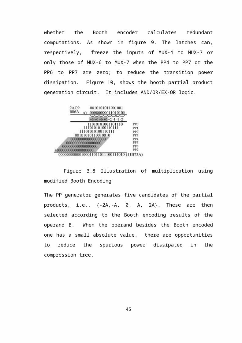
multiplying two numbers”2AC9” and “006A”. The shadow denotes that the numbers
in this part of Booth multiplication are all zero so that this part of the computations
can be neglected. Saving those computations can significantly reduce the power
consumption caused by the transient signals. According to the analysis of the
multiplication shown in figure 4, we propose the SPST-equipped modified-Booth
30
encoder, which is controlled by a detection unit. The detection unit has one of the two
operands as its input to decide whether the Booth encoder calculates redundant
computations. As shown in figure 9. The latches can, respectively, freeze the inputs
of MUX-4 to MUX-7 or only those of MUX-6 to MUX-7 when the PP4 to PP7 or the
PP6 to PP7 are zero; to reduce the transition power dissipation. Figure 10, shows the
booth partial product generation circuit. It includes AND/OR/EX-OR logic.
Figure 3.8 Illustration of multiplication using modified Booth Encoding
The PP generator generates five candidates of the partial products, i.e., {-2A,-A, 0, A,
2A}. These are then selected according to the Booth encoding results of the operand
B. When the operand besides the Booth encoded one has a small absolute value,
there are opportunities to reduce the spurious power dissipated in the compression
tree.
Figure 3.9 Modified Booth Encoder
31

3.5.2 Partial product generator
The multiplication first step generates from A and X a set of bits whose
weights sum is the product P. For unsigned multiplication, P most significant bit
weight is positive, while in 2's complement it is negative.
Figure 3.10 Booth partial product selector logic
The partial product is generated by doing AND between ‘a’ and ‘b’ which are a 4 bit
vectors as shown in fig3.6. If we take, four bit multiplier and 4-bit multiplicand we
get four partial products in which the first partial product is stored in ‘q’. Similarly,
the second, third and fourth partial products are stored in 4-bit vector n, x, y.
Figure 3.11 Booth partial product generation
32

The multiplication second step reduces the partial products from the preceding step into two
numbers while preserving the weighted sum. The sough after product P is the sum of those
two numbers. The two numbers will be added during the third step The "Wallace trees"
synthesis follows the Dadda's algorithm, which assures of the minimum counter number. If on
top of that we impose to reduce as late as (or as soon as) possible then the solution is unique.
The two binary number to be added during the third step may also be seen a one number in
CSA notation (2 bits per digit).
Figure 3.11 Booth single partial product selector logic
3.5.3 Modified Booth Encoder
Multiplication consists of three steps:
1) the first step to generate the partial products;
2) the second step to add the generated partial products until the last two rows
are remained;
3) the third step to compute the final multiplication results by adding the last
two rows.
The modified Booth algorithm reduces the number of partial products by half
in the first step. We used the modified Booth encoding (MBE) scheme proposed in. It
is known as the most efficient Booth encoding and decoding scheme. To multiply X
by Y using the modified Booth algorithm starts from grouping Y by three bits and
encoding into one of {-2, -1, 0, 1, 2}.
33

Multiply by zero means the multiplicand is multiplied by zero. Multiply by
one means the product is still the same as the multiplicand value. Multiply by -1
means that the product is the two’s complement of the multiplicand value. Multiply
by 2 is to shift left one bit of the multiplicand value whereas multiply by -2 is to shift
left one bit the two’s complement of the multiplicand value whereas multiply by -2 is
to shift left one bit the two’s complement of the multiplicand value.
34

CHAPTER 4
VHDL–XILINX & DESIGN IMPLEMENTATION ON FPGA
4.1. INTRODUCTION TO VHDL
The VHDL language and is mainly intended as a companion for the Digital
Design Laboratory. This writing aims to give the reader a quick introduction to
VHDL and to give a complete or in-depth discussion of VHDL. For a more detailed
treatment, please consult any of the many good books on this topic. Several of these
books are listed in the reference list.
4.1.1. Introduction
VHDL stands for VHSIC (Very High Speed Integrated Circuits) Hardware
Description Language. In the mid-1980’s the U.S. Department of Defense and the
IEEE sponsored the development of this hardware description language with the goal
to develop very high-speed integrated circuit. It has become now one of industry’s
standard languages used to describe digital systems. The other widely used hardware
description language is Verilog. Both are powerful languages that allow you to
describe and simulate complex digital systems. A third HDL language is ABEL
(Advanced Boolean Equation Language) which was specifically designed for
Programmable Logic Devices (PLD). ABEL is less powerful than the other two
languages and is less popular in industry. This tutorial deals with VHDL, as described
by the IEEE standard 1076-1993.
Although these languages look similar as conventional programming
languages, there are some important differences. A hardware description language is
inherently parallel, i.e. commands, which correspond to logic gates, are executed
(computed) in parallel, as soon as a new input arrives. A HDL program mimics the
behavior of a physical, usually digital, system. It also allows incorporation of timing
specifications (gate delays) as well as to describe a system as an interconnection of
different components.
35
4.1.2. Levels of representation and abstraction
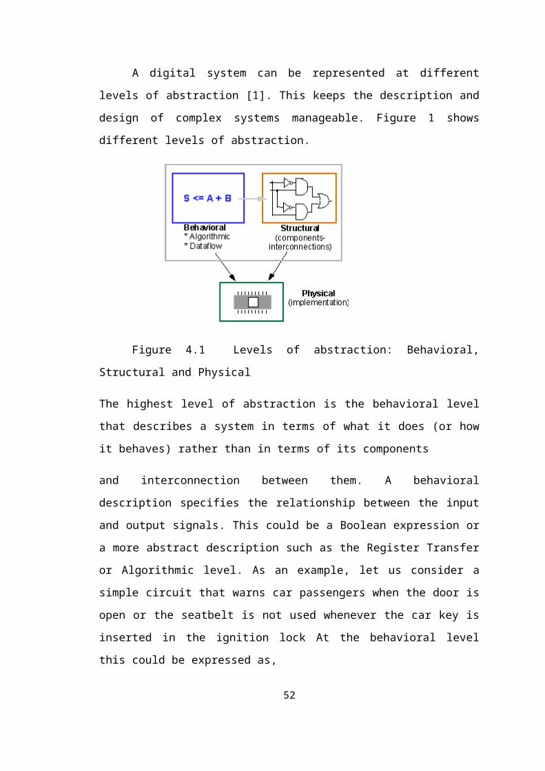
A digital system can be represented at different levels of abstraction [1]. This
keeps the description and design of complex systems manageable. Figure 1 shows
different levels of abstraction.
Figure 4.1 Levels of abstraction: Behavioral, Structural and Physical
The highest level of abstraction is the behavioral level that describes a system in terms
of what it does (or how it behaves) rather than in terms of its components
and interconnection between them. A behavioral description specifies the relationship
between the input and output signals. This could be a Boolean expression or a more
abstract description such as the Register Transfer or Algorithmic level. As an
example, let us consider a simple circuit that warns car passengers when the door is
open or the seatbelt is not used whenever the car key is inserted in the ignition lock At
the behavioral level this could be expressed as,
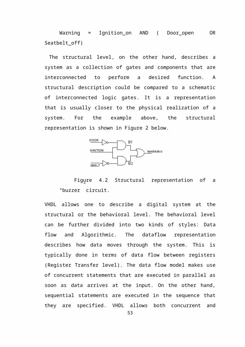
Warning = Ignition_on AND ( Door_open OR Seatbelt_off)
The structural level, on the other hand, describes a system as a collection of gates and
components that are interconnected to perform a desired function. A structural
description could be compared to a schematic of interconnected logic gates. It is a
representation that is usually closer to the physical realization of a system. For the
example above, the structural representation is shown in Figure 2 below.
36

Figure 4.2 Structural representation of a “buzzer” circuit.
VHDL allows one to describe a digital system at the structural or the behavioral level.
The behavioral level can be further divided into two kinds of styles: Data flow and
Algorithmic. The dataflow representation describes how data moves through the
system. This is typically done in terms of data flow between registers (Register
Transfer level). The data flow model makes use of concurrent statements that are
executed in parallel as soon as data arrives at the input. On the other hand, sequential
statements are executed in the sequence that they are specified. VHDL allows both
concurrent and sequential signal assignments that will determine the manner in which
they are executed. Examples of both representations will be given later.
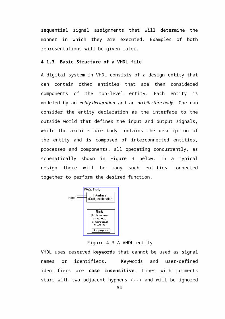
4.1.3. Basic Structure of a VHDL file
A digital system in VHDL consists of a design entity that can contain other entities
that are then considered components of the top-level entity. Each entity is modeled by
an entity declaration and an architecture body. One can consider the entity
declaration as the interface to the outside world that defines the input and output
signals, while the architecture body contains the description of the entity and is
composed of interconnected entities, processes and components, all operating
concurrently, as schematically shown in Figure 3 below. In a typical design there will
be many such entities connected together to perform the desired function.
Figure 4.3 A VHDL entity
37

VHDL uses reserved keywords that cannot be used as signal names or identifiers.
Keywords and user-defined identifiers are case insensitive. Lines with comments
start with two adjacent hyphens (--) and will be ignored by the compiler. VHDL also
ignores line breaks and extra spaces. VHDL is a strongly typed language which
implies that one has always to declare the type of every object that can have a value,
such as signals, constants and variables.
Figure 4.4 Top down design approach
4.2 Abstraction Level
VHDL supports designing at many different levels of abstraction. Three of
them are very important:
Behavioral level
Register-Transfer Level
Gate Level
38

4.2.1 Behavioral Level
This level describes a system by concurrent algorithms (Behavioral). Each
algorithm itself is sequential, that means it consists of a set of instructions that are
executed one after the other. Functions, Tasks and Always blocks are the main
elements. There is no regard to the structural realization of the design.
4.2.2 Register-Transfer Level
Designs using the Register-Transfer Level specify the characteristics of a
circuit by operations and the transfer of data between the registers. An explicit clock
is used. RTL design contains exact timing bounds: operations are scheduled to occur
at certain times. Modern RTL code definition is "Any code that is synthesizable is
called RTL code".
4.2.3 Gate Level
Within the logic level the characteristics of a system are described by logical
links and their timing properties. All signals are discrete signals. They can only have
definite logical values (`0', `1', `X', `Z`). The usable operations are predefined logic
primitives (AND, OR, NOT etc gates). Using gate level modeling might not be a good
idea for any level of logic design. Gate level code is generated by tools like synthesis
tools and this netlist is used for gate level simulation and for backend.
4.3 Introduction to FPGA
FPGA stands for Field Programmable Gate Array which has the array of logic
module, I/O module and routing tracks (programmable interconnect). FPGA can be
configured by end user to implement specific circuitry. Speed is up to 100 MHz but at
present speed is in GHz. Main applications are DSP, FPGA based computers, logic
emulation, ASIC and ASSP. FPGA can be programmed mainly on SRAM (Static
Random Access Memory). It is Volatile and main advantage of using SRAM
programming technology is re-configurability. Issues in FPGA technology are
complexity of logic element, clock support, IO support and interconnections
(Routing).
39

4.3.1 FPGA Design Flow
FPGA contains a two dimensional arrays of logic blocks and interconnections
between logic blocks. Both the logic blocks and interconnects are programmable.
Logic blocks are programmed to implement a desired function and the interconnects
are programmed using the switch boxes to connect the logic blocks. To be more clear,
if we want to implement a complex design (CPU for instance), then the design is
divided into small sub functions and each sub function is implemented using one logic
block. Now, to get our desired design (CPU), all the sub functions implemented in
logic blocks must be connected and this is done by programming the interconnects.
Internal structure of an FPGA is depicted in the following figure.
Figure 4.5 Internal structure of FPGA
FPGAs, alternative to the custom ICs, can be used to implement an entire System On
one Chip (SOC). The main advantage of FPGA is ability to reprogram. User can
reprogram an FPGA to implement a design and this is done after the FPGA is
manufactured. This brings the name “Field Programmable.”
Custom ICs are expensive and takes long time to design so they are useful
when produced in bulk amounts. But FPGAs are easy to implement with in a short
time with the help of Computer Aided Designing (CAD) tools (because there is no 40
physical layout process, no mask making, and no IC manufacturing).Some
disadvantages of FPGAs are, they are slow compared to custom ICs as they can’t
handle vary complex designs and also they draw more power.
Xilinx logic block consists of one Look Up Table (LUT) and one FlipFlop.
An LUT is used to implement number of different functionality. The input lines to the
logic block go into the LUT and enable it. The output of the LUT gives the result of
the logic function that it implements and the output of logic block is registered or
unregistered out put from the LUT.
SRAM is used to implement a LUT.A k-input logic function is implemented
using 2^k * 1 size SRAM. Number of different possible functions for k input LUT is
2^2^k. Advantage of such an architecture is that it supports implementation of so
many logic functions, however the disadvantage is unusually large number of
memory cells required to implement such a logic block in case number of inputs is
large.
Figure 4.6 4-input LUT based implementation of logic block
LUT based design provides for better logic block utilization. A k-input LUT
based logic block can be implemented in number of different ways with trade off
between performance and logic density.
An n-LUT can be shown as a direct implementation of a function truth-table.
Each of the latch holds the value of the function corresponding to one input
41
combination. For Example: 2- LUT can be used to implement 16 types of functions
like AND , OR, A+not B .... etc.
4.3.2 Inteconnects
A wire segment can be described as two end points of an interconnect with no
programmable switch between them. A sequence of one or more wire segments in an
FPGA can be termed as a track.
Typically an FPGA has logic blocks, interconnects and switch blocks
(Input/Output blocks). Switch blocks lie in the periphery of logic blocks and
interconnect. Wire segments are connected to logic blocks through switch blocks.
Depending on the required design, one logic block is connected to another and so on.
4.3.3 FPGA Design Flow
In this part of tutorial we are going to have a short intro on FPGA design flow.
A simplified version of design flow is given in the flowing diagram.
Figure 4.7 FPGA Design Flow
4.3.4 Design Entry
There are different techniques for design entry. Schematic based, Hardware
Description Language and combination of both etc. . Selection of a method depends
on the design and designer. If the designer wants to deal more with Hardware, then
42

Schematic entry is the better choice. When the design is complex or the designer
thinks the design in an algorithmic way then HDL is the better choice. Language
based entry is faster but lag in performance and density. HDLs represent a level of
abstraction that can isolate the designers from the details of the hardware
implementation. Schematic based entry gives designers much more visibility into the
hardware. It is the better choice for those who are hardware oriented. Another method
but rarely used is state-machines. It is the better choice for the designers who think the
design as a series of states. But the tools for state machine entry are limited. In this
documentation we are going to deal with the HDL based design entry.
4.3.5 Synthesis
The process which translates VHDL or Verilog code into a device netlist
formate. i.e a complete circuit with logical elements( gates, flip flops, etc…) for the
design.If the design contains more than one sub designs, ex. to implement a processor,
we need a CPU as one design element and RAM as another and so on, then the
synthesis process generates netlist for each design element Synthesis process will
check code syntax and analyze the hierarchy of the design which ensures that the
design is optimized for the design architecture, the designer has selected. The
resulting netlist(s) is saved to an NGC( Native Generic Circuit) file (for Xilinx®
Synthesis Technology (XST)).
Figure 4.8 FPGA Synthesis
4.3.6 Implementation
This process consists a sequence of three steps
43

1.Translate
2.Map
3.Place and Route
4.3.7 Translate
Process combines all the input netlists and constraints to a logic design file.
This information is saved as a NGD (Native Generic Database) file. This can be done
using NGD Build program. Here, defining constraints is nothing but, assigning the
ports in the design to the physical elements (ex. pins, switches, buttons etc) of the
targeted device and specifying time requirements of the design. This information is
stored in a file named UCF (User Constraints File). Tools used to create or modify the
UCF are PACE, Constraint Editor etc.
Figure 4.9 FPGA Translate
4.3.8 Map
Process divides the whole circuit with logical elements into sub blocks such
that they can be fit into the FPGA logic blocks. That means map process fits the logic
defined by the NGD file into the targeted FPGA elements (Combinational Logic
Blocks (CLB), Input Output Blocks (IOB)) and generates an NCD (Native Circuit
Description) file which physically represents the design mapped to the components of
FPGA. MAP program is used for this purpose.
44
4.10 FPGA Map
4.3.9 Place and Route
PAR program is used for this process. The place and route process places the
sub blocks from the map process into logic blocks according to the constraints and
connects the logic blocks. Ex. if a sub block is placed in a logic block which is very
near to IO pin, then it may save the time but it may effect some other constraint. So
trade off between all the constraints is taken account by the place and route process.
The PAR tool takes the mapped NCD file as input and produces a completely
routed NCD file as output. Output NCD file consists the routing information.
4.11 FPGA Place and Route
4.3.10 Device Programming
Now the design must be loaded on the FPGA. But the design must be
converted to a format so that the FPGA can accept it. BITGEN program deals with the
conversion. The routed NCD file is then given to the BITGEN program to generate a
bit stream (a .BIT file) which can be used to configure the target FPGA device. This
can be done using a cable. Selection of cable depends on the design.
45

4.3.11 Design Verification
Verification can be done at different stages of the process steps.
4.3.12 Behaviour Simulation(RTL Simulation)
This is first of all simulation steps; those are encountered throughout the
hierarchy of the design flow. This simulation is performed before synthesis process to
verify RTL (behavioral) code and to confirm that the design is functioning as
intended. Behavioral simulation can be performed on either VHDL or Verilog
designs. In this process, signals and variables are observed, procedures and
functions are traced and breakpoints are set. This is a very fast simulation and so
allows the designer to change the HDL code if the required functionality is not met
with in a short time period. Since the design is not yet synthesized to gate level,
timing and resource usage properties are still unknown.
4.3.13 Functional Simulation(Post Translate Simulation)
Functional simulation gives information about the logic operation of the
circuit. Designer can verify the functionality of the design using this process after the
Translate process. If the functionality is not as expected, then the designer has to
made changes in the code and again follow the design flow steps.
4.3.14 Static Timing Analysis
This can be done after MAP or PAR processes Post MAP timing report lists
signal path delays of the design derived from the design logic. Post Place and Route
timing report incorporates timing delay information to provide a comprehensive
timing summary of the design.
4.4 XILINX
Xilinx is the world's largest supplier of programmable logic devices, the
inventor of the field programmable gate array (FPGA) and the first semiconductor
company with a fables manufacturing model.
The Xilinx software can do simulation and synthesis .The entire processor will
be implemented using the Xilinx FPGAs. So it won’t spend much time to wiring up
46

that part of the circuit. However, the designer have to wire the switches and lights that
are used to control the processor, and have to wire the Xilinx part itself to the
switches and lights, but this shouldn't be too bad. The designer will also use the
backplane bus in the lab kit so that the Triscuit will be built on two boards: one for the
Xilinx chip, and one for the switches and lights. The HDL Editor feature provides
extensive edit and search capabilities with language- specific color coding of
keywords, as well as integrated on-line syntax checking to scan VHDL code for
errors. The Language Assistant feature speeds design entry by providing a lookup list
of typical language constructs and commonly used synthesis modules like counters,
accumulators, and adders.
4.4.1 XST Design Flow Overview
The following figure shows the flow of files through the XST software.
Design Entry Overview. Design entry can create source files to represent the design.
The top-level design source file can be any of the following formats:
Hardware Description Language (HDL), such as VHDL or Verilog
Schematic (SCH)
Embedded processor (XMP)
4.4.2 ISE Design Suite
The ISE Design Suite: Logic Edition allows you to go from design entry,
through implementation and verification, to device programming from within the
unified environment of the ISE Project Navigator or from the command line. This
edition includes exclusive tools and technologies to help achieve optimal design
results, including the following:
Xilinx Synthesis Technology (XST) - synthesizes VHDL, Verilog, or mixed
language designs.
ISim - enables you to perform functional and timing simulations for VHDL,
Verilog and mixed VHDL/Verilog designs.
47

Plan Ahead software - enables you to do advanced FPGA floor planning. The
Plan Ahead software includes I/O Planner, an environment designed to help you to
import or create Ahead software includes I/O Planner, an environment designed to
help you to import or create the initial I/O Port list, group the related ports into
separate folders called “Interfaces” and assign them to package pins. I/O Planner
supports fully automatic pin placement or semi- automated interactive modes to allow
controlled I/O Port assignment. With early, intelligent decisions in FPGA I/O
assignments, you can more easily optimize the connectivity between the PCB and
FPGA.
CORE Generator software - provides an extensive library of Xilinx LogiCORE IP
from basic elements to complex, system level IP cores.
Smart Guide technology - enables you to use results from a previous
implementation to guide the next implementation for faster incremental
implementation.
Design Preservation - enables you to use placement and routing for unchanged
blocks from a previous implementation to reduce iterations in the timing closure
phase.
Partial Reconfiguration - enables dynamic design modification of a configured
FPGA. The ISE software uses Partition technology to define and implement static and
reconfigurable regions of the device. This feature requires an additional license code.
XPower Analyzer enables you to analyze power consumption for Xilinx FPGA
and CPLD devices.
Power Optimization for Virtex-6 devices minimizes logic toggling to reduce
dynamic power consumption.
IMPACT enables you to directly configure Xilinx FPGAs or program Xilinx
CPLDs and PROMs with the Xilinx cables. It also enables you to create programming
files, read back and verify design configuration data, debug configuration problems,
and execute SVF and XSVF files.
48

ChipScope Protocol assists with in circuit verification. Note Design Preservation
and Partial Reconfiguration are supported for the command line tools and the
standalone version of the PlanAhead software.
Figure 4.12 Properties of Device Parameters
4.4.3 Process Window
The processes windows list the available processes (corresponding to the
process selected in the processes window). Typically you will select a particular
process that you want to perform on the selected source file This can include a
simulation, implementation, etc. To run a process you can double click on the process.
When a process has been successfully executed a red tick-off icon appears. When you
run a high-level process, the Project Navigator will automatically run all the
associated lower-level processes.
Integrated Software Environment (ISE) is the Xilinx design software suite.
This overview explains the general progression of a design through ISE from start to
finish. ISE enables the design to be initiated with any of a number of different source
types, including:
HDL (VHDL, Verilog HDL, ABEL)
49

Schematic design files
EDIF
State Machines
IP Cores
From source files, ISE enables quick verification of the functionality of these sources
using the integrated simulation capabilities, including ModelSim Xilinx Edition and
the HDL Bencher test bench generator. HDL sources may be synthesized using the
Xilinx Synthesis Technology (XST) as well as partner synthesis engines used
standalone or integrated into ISE. The Xilinx implementation tools continue the
process into a placed and routed FPGA or fitted CPLD, and finally produce a bit
stream for the device configuration.
4.4.4 Design Entry
1. ISE Text Editor - The ISE Text Editor is provided in ISE for entering design code
and viewing reports.
2. Schematic Editor - The Engineering Capture System (ECS) is a graphical user
interface (GUI) that allows creating, viewing, and editing schematics and symbols for
the Design Entry step of the Xilinx design flow.
3. CORE Generator - The CORE Generator System is a design tool that delivers
parameterized cores optimized for Xilinx FPGAs ranging in complexity from simple
arithmetic operators such as adders, to system-level building blocks such as filters,
transforms, FIFOs, and memories.
4. Constraints Editor - The Constraints Editor allows to create and modify the most
commonly used timing constraints.
5. PACE - The Pin out and Area Constraints Editor (PACE) allows viewing and
editing I/O, Global logic, and Area Group constraints.
6. State CAD State Machine Editor - State CAD allows to specify states, transitions,
and actions in a graphical editor. The state machine will be created in HDL.
50

4.4.5 Implementation
1. Translate - The Translate process runs NGD Build to merge all of the input net
lists as well as design constraint information into a Xilinx database file.
2. Map - The Map program maps a logical design to a Xilinx FPGA.
3. Place and Route (PAR) - The PAR program accepts the mapped design, places and
routes the FPGA, and produces output for the bit stream generator.
4. Floor planner - The Floor planner allows viewing a graphical representation of the
FPGA, and to view and modify the placed design.
5. FPGA Editor - The FPGA Editor allows viewing and modifying the physical
implementation, including routing.
6. Timing Analyzer - The Timing Analyzer provides a way to perform static timing
analysis on FPGA and CPLD designs. With Timing Analyzer, analysis can be
performed immediately after mapping, placing or routing an FPGA design, and after
fitting and routing a CPLD design.
4.4.6 Features
• Memory Editor Window.
• Post Map and Post Translate flow supported in Project Navigator.
• Support of simulation of Embedded designs in XPS and Project Navigator
• ISim Hardware Co-Simulation Limited Access feature.
4.5 Introduction to XILINX’s Spartan-3 Kit
The Spartan-3 family of Field Programmable Gate Arrays is specifically
designed to meet the needs of high volume, cost sensitive consumer electronic
applications. The eight member family offers densities ranging from 50,000 to five
million system gates.
The Spartan-3 family builds on the success of the earlier Spartan-IIE family by
increasing the amount of logic resources, the capacity of internal RAM, the total
51
number of I/Os, and the overall level of performance as well as by improving clock
management functions. Numerous enhancements derive from the Virtex-II platform
technology. These Spartan-3 FPGA enhancements, combined with advanced process
technology, deliver more functionality and bandwidth per dollar than was previously
possible, setting new standards in the programmable logic industry. Because of their
exceptionally low cost, Spartan-3 FPGAs are ideally suited to a wide range of
consumer electronics applications; including broadband access, home networking,
display/projection and digital television equipment. The Spartan-3 family is a superior
alternative to mask programmed ASICs. FPGAs avoid the high initial cost, the
lengthy development cycles, and the inherent inflexibility of conventional ASICs.
Also, FPGA programmability permits design upgrades in the field with no hardware
replacement.
Figure 4.13 Spartan-3 FPGA Kit52
4.6 Boundary Scan (JTAG) Mode
In Boundary Scan mode, dedicated pins are used for configuring the FPGA.
The configuration is done entirely through the IEEE 1149.1 Test Access Port (TAP).
FPGA configuration using the Boundary Scan mode is compatible with the IEEE STD
1149.1-1993 standard and IEEE Std 1532 for In System Configurable (ISC) devices.
Configuration through the Boundary Scan port is always available, regardless of the
selected configuration mode. In some cases, however, the mode pin setting may
affect proper programming of the device due to various interactions.
For example, if the mode pins are set to Master Serial or Master Parallel mode,
and the associated PROM is already programmed with a valid configuration image,
then there is potential for configuration interference between the JTAG and PROM
data. Selecting the Boundary Scan mode disables the other modes and is the most
reliable mode when programming via JTAG.
4.7 Swithces,Buttons And Knob
4.7.1 Slide Switches
The Spartan-3 Starter Kit board has eight slide switches. The slide switches
are located in the lower right corner of the board and are labeled SW7 through SW0.
Switch SW7 is the left- most switch, and SW0 is the right-most switch.
Figure 4.14 Slide Switches
Operation : When in the UP or ON position, a switch connects the FPGA pin to 3.3V,
a logic High. When DOWN or in the OFF position, the switch connects the FPGA pin
to ground, a logic Low. The switches typically exhibit about 2 ms of mechanical
bounce and there is no active de- bouncing circuitry, although such circuitry could
easily be added to the FPGA design programmed on the board.
53
4.7.2 Push Button Switches
The Spartan-3 Starter Kit board has eight momentary contact push-button
switches. The push buttons are located in the lower left corner of the board.
Figure 4.15 Push Button Switches
Operation: Pressing a push button connects the associated FPGA pin to 3.3V. Use an
internal pull- down resistor within the FPGA pin to generate a logic Low when the
button is not pressed. There is active de-bouncing circuitry on the push button.
4.7.3 Discrete LEDs
The Spartan-3 Starter Kit board has eight individual surface mount LEDs
located above the slide switches. The LEDs are labeled LED7 through LED0. LED7
is the left-most LED, LED0 the right-most LED.
Figure 4.16 Discrete LEDs
Operation : Each LED has one side connected to ground and the other side connected
to a pin on the Spartan-3 device via a 390 current limiting resistor. To light an
individual LED, drive the associated FPGA control signal High.
4.8 Clock Connections
Each of the clock inputs connect directly to a global buffer input in I/O Bank
0, along the top of the FPGA. Each of the clock inputs also optimally connects to an
associated DCM.
4.9 Voltage Control
54

The voltage for all I/O pins in FPGA I/O Bank 0 is controlled by jumper
JP9. Consequently, these clock resources are also controlled by jumper JP9. By
default, JP9 is set for 3.3 V. The on-board oscillator is a 3.3V device and might not
perform as expected when jumper JP9 is set for 2.5V.
4.10 Auxillary Clock Oscillatory Socket
The provided 8-pin socket accepts clock oscillators that fit the 8-pin DIP
footprint. Use this socket if the FPGA application requires a frequency other than
50MHz. Alternatively, use the FPGA’s Digital Clock Manager (DCM) to generate or
synthesize other frequencies from the on board 50 MHz oscillator.
CHAPTER 5
SIMULATION AND SYNTHESIS
5.1 Simulation results
We simulate the structures using ModelSim software .The outputs shown here are
obtained by using ModelSim software.
55
Figure 5.1-Simulation result for All Signals of MAC
56
Figure5.2-Simulation result of Adder
Figure 5.3-Simulation result for Booth Encoder
Figure 5.4-Simulation result for Booth Multiplier
57
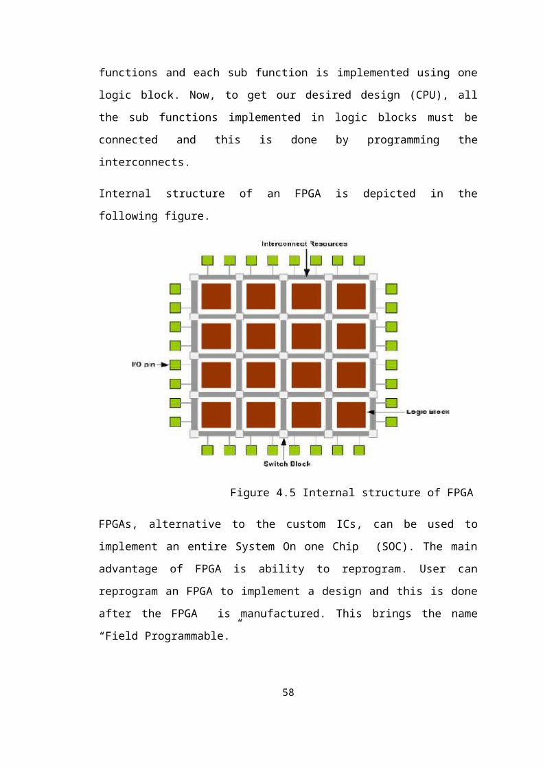
Figure 5.5-Simulation result for Full Adder
Figure 5.6-Simulation result for Half Adder
Figure 5.7-Simulation result for Booth Top-Level Module
58
5.2 SYNTHESIS REPORT
5.2.1 Synthesis Options Summary
---- Source Parameters
Input File Name : "imp_mactop_tb.prj"
Input Format : mixed
Ignore Synthesis Constraint File : NO
---- Target Parameters
Output File Name : "imp_mactop_tb"
Output Format : NGC
Target Device : xc3s500e-4-fg320
---- Source Options
Top Module Name : imp_mactop_tb
Automatic FSM Extraction : YES
FSM Encoding Algorithm : Auto
Safe Implementation : No
FSM Style : lut
RAM Extraction : Yes
RAM Style : Auto
ROM Extraction : Yes
Mux Style : Auto
Decoder Extraction : YES
Priority Encoder Extraction : YES
59

Shift Register Extraction : YES
Logical Shifter Extraction : YES
XOR Collapsing : YES
ROM Style : Auto
Mux Extraction : YES
Resource Sharing : YES
Asynchronous To Synchronous : NO
Multiplier Style : auto
Automatic Register Balancing : No
---- Target Options
Add IO Buffers : YES
Global Maximum Fanout : 500
Add Generic Clock Buffer(BUFG) : 24
Register Duplication : YES
Slice Packing : YES
Optimize Instantiated Primitives : NO
Use Clock Enable : Yes
Use Synchronous Set : Yes
Use Synchronous Reset : Yes
Pack IO Registers into IOBs : auto
Equivalent register Removal : YES
---- General Options
60

Optimization Goal : Speed
Optimization Effort : 1
Library Search Order : imp_mactop_tb.lso
Keep Hierarchy : NO
Netlist Hierarchy : as_optimized
RTL Output : Yes
Global Optimization : AllClockNets
Read Cores : YES
Write Timing Constraints : NO
Cross Clock Analysis : NO
Hierarchy Separator : /
Bus Delimiter : <>
Case Specifier : maintain
Slice Utilization Ratio : 100
BRAM Utilization Ratio : 100
Verilog 2001 : YES
Auto BRAM Packing : NO
Slice Utilization Ratio Delta : 5
5.2.2 HDL Synthesis Report
Macro Statistics
# ROMs : 8
8x1-bit ROM : 8
61

# Accumulators : 1
32-bit up accumulator : 1
# Registers : 3
1-bit register : 1
16-bit register : 2
# Multiplexers : 136
1-bit 8-to-1 multiplexer : 136
# Xors : 200
1-bit xor2 : 32
1-bit xor3 : 168
5.2.3 Advanced HDL Synthesis Report
Macro Statistics
# ROMs : 8
8x1-bit ROM : 8
# Accumulators : 1
32-bit up accumulator : 1
# Registers : 33
Flip-Flops : 33
# Multiplexers : 136
1-bit 8-to-1 multiplexer : 136
# Xors : 200
1-bit xor2 : 32
62

1-bit xor3 : 168
5.2.4 Final Report
Found area constraint ratio of 100 (+ 5) on block imp_mactop_tb, actual ratio is
3.Final Macro Processing ...
Final Register Report
Macro Statistics
# Registers : 36
Flip-Flops : 36
Final Results
RTL Top Level Output File Name : imp_mactop_tb.ngr
Top Level Output File Name : imp_mactop_tb
Output Format : NGC
Optimization Goal : Speed
Keep Hierarchy : NO
Design Statistics
# IOs : 5
Cell Usage :
# BELS : 116
# GND : 1
# INV : 1
# LUT1 : 3
# LUT2 : 3
# LUT3 : 7
63
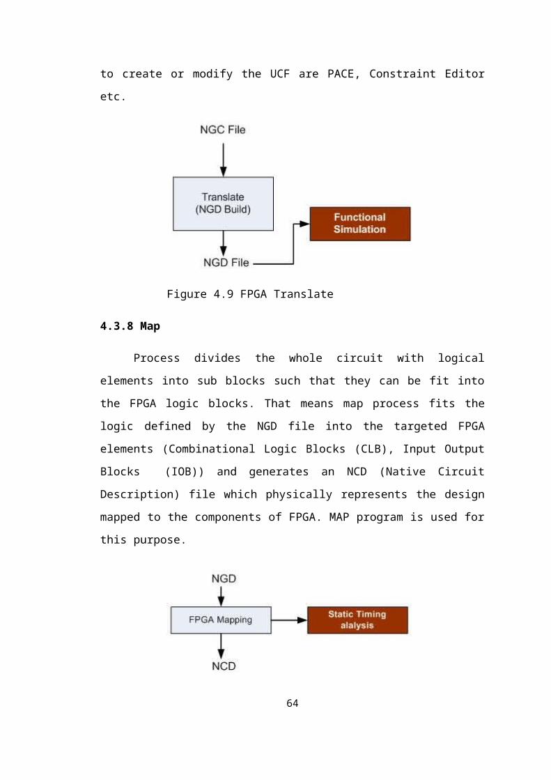
# LUT4 : 29
# MUXCY : 39
# VCC : 1
# XORCY : 32
# FlipFlops/Latches : 36
# FDC : 35
# FDE : 1
# Clock Buffers : 1
# BUFGP : 1
# IO Buffers : 4
# IBUF : 3
# OBUF : 1
Device utilization summary:
Selected Device : 3s500efg320-4
Number of Slices: 23 out of 4656 0%
Number of Slice Flip Flops: 36 out of 9312 0%
Number of 4 input LUTs: 43 out of 9312 0%
Number of IOs: 5
Number of bonded IOBs: 5 out of 232 2%
Number of GCLKs: 1 out of 24 4%
TIMING REPORT
Timing Summary:
64
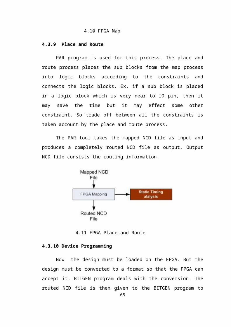
Speed Grade: -4
Minimum period: 5.921ns (Maximum Frequency: 168.890MHz)
Minimum input arrival time before clock: 4.160ns
Maximum output required time after clock: 4.283ns
Maximum combinational path delay: No path found
Timing Detail:
All values displayed in nanoseconds (ns)
Timing constraint: Default period analysis for Clock 'clk'
Clock period: 5.921ns (frequency: 168.890MHz)
Total number of paths / destination ports: 2207 / 33
Delay: 5.921ns (Levels of Logic = 32)
Source: breg_5 (FF)
Destination: uut/mul_out_r_31 (FF)
Source Clock: clk rising
Destination Clock: clk rising
Total 5.921ns (4.582ns logic, 1.339ns route)
(77.4% logic, 22.6% route)
Timing constraint: Default OFFSET IN BEFORE for Clock 'clk'
Total number of paths / destination ports: 6 / 4
Offset: 4.160ns (Levels of Logic = 2)
Source: rst (PAD)
Destination: macout_reg (FF)
65

Destination Clock: clk rising
Data Path: rst to macout_reg
Gate Net
Cell:in->out fanout Delay Delay Logical Name (Net Name)
IBUF:I->O 36 1.218 1.263 rst_IBUF (rst_IBUF)
INV:I->O 1 0.704 0.420 rst_inv1_INV_0 (rst_inv)
FDE:CE 0.555 macout_reg
Total 4.160ns (2.477ns logic, 1.683ns route)
(59.5% logic, 40.5% route)
Timing constraint: Default OFFSET OUT AFTER for Clock 'clk'
Total number of paths / destination ports: 1 / 1
Offset: 4.283ns (Levels of Logic = 1)
Source: macout_reg (FF)
Destination: macout1 (PAD)
Source Clock: clk rising
Data Path: macout_reg to macout1
Gate Net
Cell:in->out fanout Delay Delay Logical Name (Net Name)
FDE:C->Q 1 0.591 0.420 macout_reg (macout_reg)
OBUF:I->O 3.272 macout1_OBUF (macout1)
Total 4.283ns (3.863ns logic, 0.420ns route)
(90.2% logic, 9.8% route)
66

Total memory usage is 140792 kilobytes
Number of errors : 0 ( 0 filtered)
Number of warnings : 40 ( 0 filtered)
Number of infos : 5 ( 0 filtered)
5.3 Synthesis Results
Figure 5.8 RTL of Adder unit
67
Figure 5.9 Internal Structure of RTL Top module
Figure 5.10 RTL of Booth Multiplier
68

Figure 5.11 RTL of Booth Encoder
Figure 5.12 Internal RTL of Multiplier
69
Figure 5.13 RTL schematic of Top module
Figure 5.14 RTL Internal Structure of Adder block
70
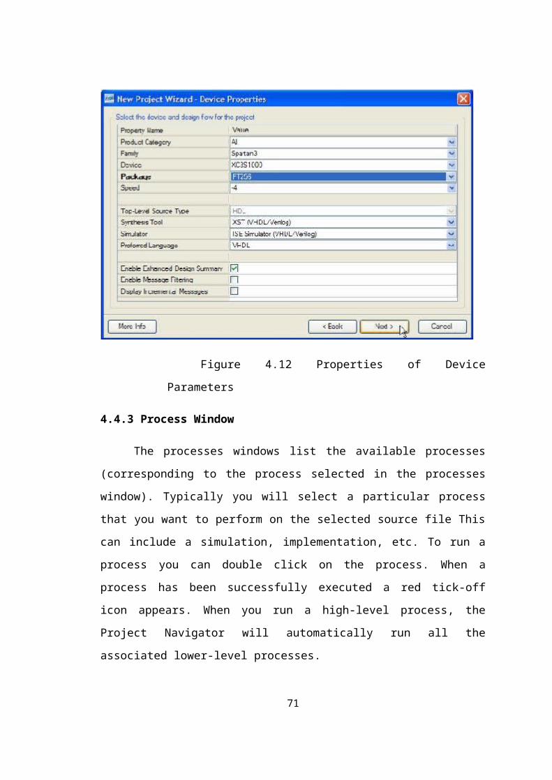
CHAPTER 6
CONCLUSION AND FUTURE WORK
A 16x16 multiplier-accumulator (MAC) is presented in this work. A RADIX
4Modified Booth multiplier circuit is used for MAC architecture. Compared to other
circuits, the Booth multiplier has the highest operational speed and less hardware
count. The basic building blocks for the MAC unit are identified and each of the
blocks is analyzed for its performance. Power and delay is calculated for the blocks.
1-bit MAC unit is designed with enable to reduce the total power consumption based
on block enable technique. Using this block, the N-bit MAC unit is constructed and
the total power consumption is calculated for the MAC unit. The power reduction
techniques adopted in this work. The MAC unit designed in this work can be used in
filter realizations for High speed DSP applications.
71

BIBLIOGRAPHY
[1] J.J.FCavanagh,Digital Computer Arithmetic. New York:McGraw-Hill,1984
[2] Information Technology-Coding of Moving Picture and Associated Auto,MPEG-2
Draft International Standard,ISO/IEC 13818-1,2,31994.
[3] JPEG 2000 Part 1 Final 119l Draft,ISO/IEC JTC1/SC29 WGI.
[4] O.L.MacSorely,”High speed arithmetic in binary computers,” Proc.IRE, vol. 49,
pp.67-91,Jan. 1961.
[5] S.Waser and M.J.Flynn,Introduction to Arithmetic for Digital System Designers.
New York:Holt,Rinehart and Winston,1982.
[6] A.R.Omondi,Computer Arithmetic Systems. Englewood Cliffs,NJ:Prentice-
Hall,1994, 1994.
[7] A.D.Booth,”A signed binary multiplication technique,” Quart. J.Math., vol-
4,pp.236-240,1952.
[8] C.S.Wallace,”A suggestion for a fast multiplier,” IEEE Trans, Electron
Comput.,vol. EC-13 no.1 ,pp.14-17,Feb. 1964.
[9] A.R.Cooper, “Parallel architecture modified Booth multiplier,” Proc. Inst. Electr.
Eng. G vol. 135, pp. 125-128, 1988.
[10] N.R. Shanbag and P.Juneja , “Paralel implementation of a 4*4-bit multiplier
using modified Booth’s algorithm,” IEEE J. Solid-State Circuits ,vol.27,no.9,pp.
1229-1236,Sep. 1992.
[11] G.Goto,T.Sato,M.Nakajima,and T. Sukemura, “A 54*54 regular structured tree
multiplier,” IEEE J.Solis State Circuits,vol. 27,no. 9,pp. 1229-1236,Sep.1992.
72
[12] J. Fadavi-Ardekani,”M*N Booth encoded multiplier generator using optimized
Wallace trees,” IEEE Trans. Very Large Scale Integer.(VLSI) Syst., vol. 1,no. 2,pp.
120-125,Jun. 1993
[13] N. Ohkubo,M. Suzuki,T. Shinbo, T.Yamanaka,A.Shimizu,K.Sasaki and Y.
Nakagone,”A 4.4ns CMOS 54*54 multiplier using pass-transistor multiplexer,” IEEE
J.Solid State Circuits, vol. 30,no.3,pp. 251-257, Mar. 1995
[14] A. Tawfik, F.Elguibaly, and P. Agathoklis, “New realization and implementation
of fixed-point IIR digital filters,” J.Circuits, Syst., vol. 7,no. 3,pp. 187-191,1994.
[15] A. Tawfik, F. Elguibaly, M. N. Fahmi, E. Abdel-Raheem, and P.Agathoklis,
“High-speed area-efficient inner-product processor,” Can.J. Electr. Comput. Eng.,
vol.19,pp. 187-191, 1994.
[16] F.Elguibaly and A. Rayhan, “Overflow handling in inner-product processors,” in
Proc. IEEE Pacific Rim Conf. Commun., Comput., Signal Process.,Aug. 1997,pp.
117-120.
[17] F.Elguibaly, “A fast parallel multiplier-accumulator using the modified Booth
algorithm,” IEEE Trans. Circuits Syst., vol. 27, no. 9,pp. 902-908, Sep. 2000.
[18] A. Faye and M. Bayoumi, “A merged multiplier-accumulator for high speed
signal processing applications,” Proc. ICASSP, vol. 3,pp.3212-3215 2002.
[19] P. Zicari, S. Perri, P. Corsonello, and G. Cocorullo, “An optimized adder
accumulator for high speed MACs,” Proc. ASICON 2005, vol.2, pp. 757-760, 2005.
[20] T.Sakurai and A. R. Newton, “Alpha-power law MOSFET model and its
applications to CMOS and other formulas,” IEEE J.Solid-State Circuits, vol. 25, no.
2,pp. 584-594, Feb. 1990.
73


![Untitled Document [] · 2019. 8. 19. · Title: Untitled Document Created Date: 8/27/1999 4:18:00 PM](https://img.pdfslide.us/doc/110x75/60302906c35f694ee505573d/untitled-document-2019-8-19-title-untitled-document-created-date-8271999.jpg)