Embed Size (px)
Citation preview
TLC548C, TLC548I, TLC549C, TLC549I8-BIT ANALOG-TO-DIGITAL CONVERTERS
WITH SERIAL CONTROL
SLAS067C – NOVEMBER 1983 – REVISED SEPTEMBER 1996
1POST OFFICE BOX 655303 • DALLAS, TEXAS 75265
Microprocessor Peripheral or StandaloneOperation
8-Bit Resolution A/D Converter
Differential Reference Input Voltages
Conversion Time . . . 17 µs Max
Total Access and Conversion Cycles PerSecond
– TLC548 . . . up to 45 500– TLC549 . . . up to 40 000
On-Chip Software-ControllableSample-and-Hold Function
Total Unadjusted Erro r . . . ±0.5 LSB Max
4-MHz Typical Internal System Clock
Wide Supply Rang e . . . 3 V to 6 V
Low Power Consumptio n . . . 15 mW Max
Ideal for Cost-Effective, High-PerformanceApplications including Battery-OperatedPortable Instrumentation
Pinout and Control Signals CompatibleWith the TLC540 and TLC545 8-Bit A/DConverters and with the TLC1540 10-BitA/D Converter
CMOS Technology
description
The TLC548 and TLC549 are CMOS analog-to-digital converter (ADC) integrated circuits built around an 8-bitswitched-capacitor successive-approximation ADC. These devices are designed for serial interface with amicroprocessor or peripheral through a 3-state data output and an analog input. The TLC548 and TLC549 useonly the input/output clock (I/O CLOCK) input along with the chip select (CS) input for data control. Themaximum I/O CLOCK input frequency of the TLC548 is 2.048 MHz, and the I/O CLOCK input frequency of theTLC549 is specified up to 1.1 MHz.
AVAILABLE OPTIONS
PACKAGE
TA SMALL OUTLINE(D)
PLASTIC DIP(P)
0°C to 70°CTLC548CDTLC549CD
TLC548CPTLC549CP
–40°C to 85°CTLC548IDTLC549ID
TLC548IPTLC549IP
Copyright 1996, Texas Instruments IncorporatedPRODUCTION DATA information is current as of publication date.Products conform to specifications per the terms of Texas Instrumentsstandard warranty. Production processing does not necessarily includetesting of all parameters.
Please be aware that an important notice concerning availability, standard warranty, and use in critical applications ofTexas Instruments semiconductor products and disclaimers thereto appears at the end of this data sheet.
1
2
3
4
8
7
6
5
REF+ANALOG IN
REF–GND
VCCI/O CLOCKDATA OUTCS
D OR P PACKAGE(TOP VIEW)
TLC548C, TLC548I, TLC549C, TLC549I8-BIT ANALOG-TO-DIGITAL CONVERTERSWITH SERIAL CONTROL
SLAS067C – NOVEMBER 1983 – REVISED SEPTEMBER 1996
2 POST OFFICE BOX 655303 • DALLAS, TEXAS 75265
description (continued)
Operation of the TLC548 and the TLC549 is very similar to that of the more complex TLC540 and TLC541devices; however, the TLC548 and TLC549 provide an on-chip system clock that operates typically at 4 MHzand requires no external components. The on-chip system clock allows internal device operation to proceedindependently of serial input/output data timing and permits manipulation of the TLC548 and TLC549 as desiredfor a wide range of software and hardware requirements. The I/O CLOCK together with the internal system clockallow high-speed data transfer and conversion rates of 45 500 conversions per second for the TLC548, and40 000 conversions per second for the TLC549.
Additional TLC548 and TLC549 features include versatile control logic, an on-chip sample-and-hold circuit thatcan operate automatically or under microprocessor control, and a high-speed converter with differentialhigh-impedance reference voltage inputs that ease ratiometric conversion, scaling, and circuit isolation fromlogic and supply noises. Design of the totally switched-capacitor successive-approximation converter circuitallows conversion with a maximum total error of ±0.5 least significant bit (LSB) in less than 17 µs.
The TLC548C and TLC549C are characterized for operation from 0°C to 70°C. The TLC548I and TLC549I arecharacterized for operation from –40°C to 85°C.
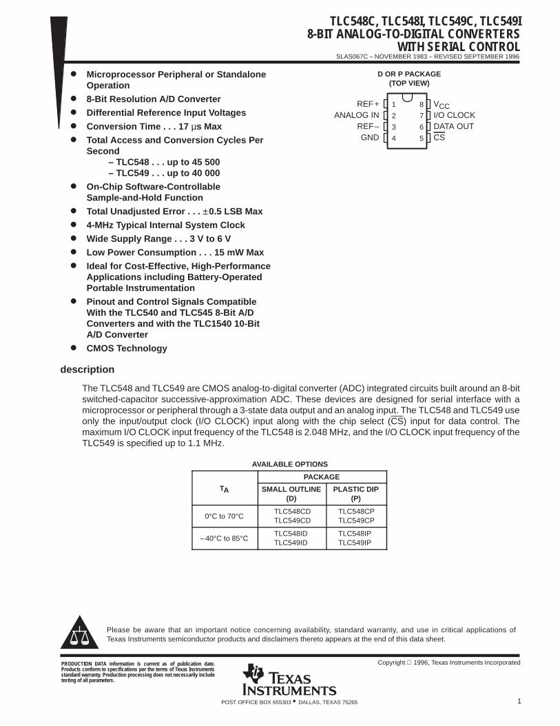
functional block diagram
REF–
64
8
8
DATAOUT
8-BitAnalog-to
DigitalConverter(Switched-Capacitors)
8-to-1 DataSelector
andDriver
OutputData
Regiser
InternalSystemClock
SampleandHold
7
5
2
3
1
ANALOG IN
REF+
CS
I/O CLOCK
ControlLogic and
Output Counter
typical equivalent inputs
INPUT CIRCUIT IMPEDANCE DURING SAMPLING MODE INPUT CIRCUIT IMPEDANCE DURING HOLD MODE
1 kΩ TYP
Ci = 60 pF TYP(equivalent inputcapacitance)
5 MΩ TYP
ANALOG IN ANALOG IN
TLC548C, TLC548I, TLC549C, TLC549I8-BIT ANALOG-TO-DIGITAL CONVERTERS
WITH SERIAL CONTROL
SLAS067C – NOVEMBER 1983 – REVISED SEPTEMBER 1996
3POST OFFICE BOX 655303 • DALLAS, TEXAS 75265
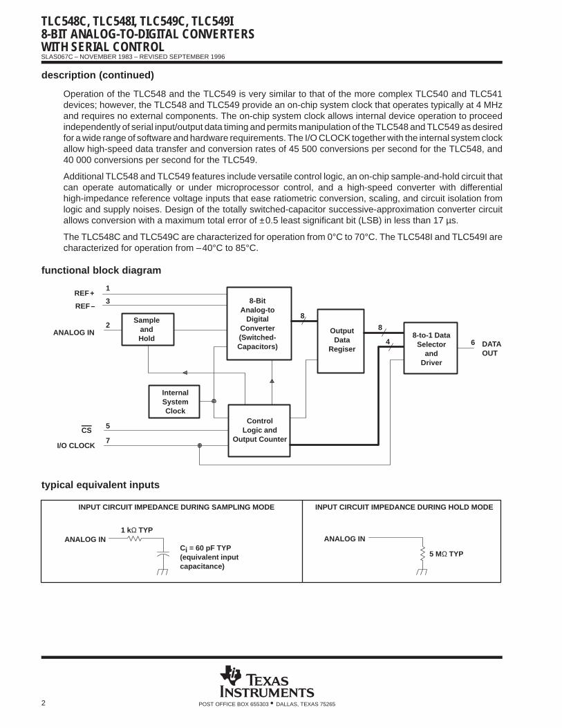
operating sequence
tenten
tsu(CS)
B7
B0B1B2B3B4B5B6B7
Conversion Data BMSBMSB LSB
Hi-Z State
MSBLSB(see Note B)MSB
Previous Conversion Data AA7
A7 A6 A5 A4 A3 A2 A1 A0
Hi-Z State
Don’t
11
(see Note A)
tconvtsu(CS)
AccessCycle B
8 8765432765432
CLOCKI/O
CS
OUTDATA
Care
SampleCycle B
AccessCycle C
SampleCycle C
twH(CS)
NOTES: A. The conversion cycle, which requires 36 internal system clock periods (17 µs maximum), is initiated with the eighth I/O clock pulsetrailing edge after CS goes low for the channel whose address exists in memory at the time.
B. The most significant bit (A7) is automatically placed on the DATA OUT bus after CS is brought low. The remaining seven bits (A6–A0)are clocked out on the first seven I/O clock falling edges. B7–B0 follows in the same manner.
absolute maximum ratings over operating free-air temperature range (unless otherwise noted)
Supply voltage, VCC (see Note 1) 6.5 V. . . . . . . . . . . . . . . . . . . . . . . . . . . . . . . . . . . . . . . . . . . . . . . . . . . . . . . . . . Input voltage range at any input –0.3 V to VCC + 0.3 V. . . . . . . . . . . . . . . . . . . . . . . . . . . . . . . . . . . . . . . . . . . . . Output voltage range –0.3 V to VCC + 0.3 V. . . . . . . . . . . . . . . . . . . . . . . . . . . . . . . . . . . . . . . . . . . . . . . . . . . . . . Peak input current range (any input) ±10 mA. . . . . . . . . . . . . . . . . . . . . . . . . . . . . . . . . . . . . . . . . . . . . . . . . . . . . Peak total input current range (all inputs) ±30 mA. . . . . . . . . . . . . . . . . . . . . . . . . . . . . . . . . . . . . . . . . . . . . . . . . Operating free-air temperature range, TA (see Note 2): TLC548C, TLC549C 0°C to 70°C. . . . . . . . . . . . .
TLC548I, TLC549I –40°C to 85°C. . . . . . . . . . . . Storage temperature range, Tstg –65°C to 150°C. . . . . . . . . . . . . . . . . . . . . . . . . . . . . . . . . . . . . . . . . . . . . . . . . . Lead temperature 1,6 mm (1/16 inch) from case for 10 seconds 260°C. . . . . . . . . . . . . . . . . . . . . . . . . . . . . . .
NOTES: 1. All voltage values are with respect to the network ground terminal with the REF– and GND terminals connected together, unlessotherwise noted.
2. The D package is not recommended below –40°C.
TLC548C, TLC548I, TLC549C, TLC549I8-BIT ANALOG-TO-DIGITAL CONVERTERSWITH SERIAL CONTROL
SLAS067C – NOVEMBER 1983 – REVISED SEPTEMBER 1996
4 POST OFFICE BOX 655303 • DALLAS, TEXAS 75265
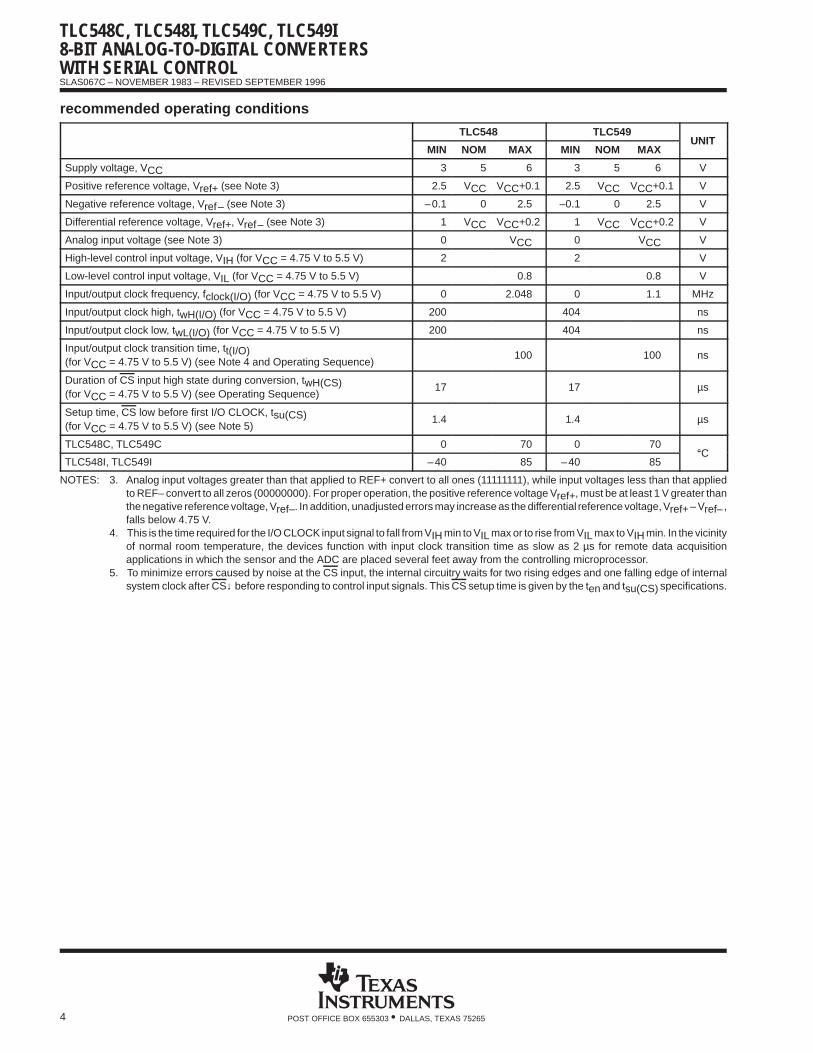
recommended operating conditions
TLC548 TLC549UNIT
MIN NOM MAX MIN NOM MAXUNIT
Supply voltage, VCC 3 5 6 3 5 6 V
Positive reference voltage, Vref+ (see Note 3) 2.5 VCC VCC+0.1 2.5 VCC VCC+0.1 V
Negative reference voltage, Vref– (see Note 3) –0.1 0 2.5 –0.1 0 2.5 V
Differential reference voltage, Vref+, Vref– (see Note 3) 1 VCC VCC+0.2 1 VCC VCC+0.2 V
Analog input voltage (see Note 3) 0 VCC 0 VCC V
High-level control input voltage, VIH (for VCC = 4.75 V to 5.5 V) 2 2 V
Low-level control input voltage, VIL (for VCC = 4.75 V to 5.5 V) 0.8 0.8 V
Input/output clock frequency, fclock(I/O) (for VCC = 4.75 V to 5.5 V) 0 2.048 0 1.1 MHz
Input/output clock high, twH(I/O) (for VCC = 4.75 V to 5.5 V) 200 404 ns
Input/output clock low, twL(I/O) (for VCC = 4.75 V to 5.5 V) 200 404 ns
Input/output clock transition time, tt(I/O) (for VCC = 4.75 V to 5.5 V) (see Note 4 and Operating Sequence)
100 100 ns
Duration of CS input high state during conversion, twH(CS)(for VCC = 4.75 V to 5.5 V) (see Operating Sequence)
17 17 µs
Setup time, CS low before first I/O CLOCK, tsu(CS) (for VCC = 4.75 V to 5.5 V) (see Note 5)
1.4 1.4 µs
TLC548C, TLC549C 0 70 0 70°C
TLC548I, TLC549I –40 85 –40 85°C
NOTES: 3. Analog input voltages greater than that applied to REF+ convert to all ones (11111111), while input voltages less than that appliedto REF– convert to all zeros (00000000). For proper operation, the positive reference voltage Vref+, must be at least 1 V greater thanthe negative reference voltage, Vref–. In addition, unadjusted errors may increase as the differential reference voltage, Vref+ – Vref– ,falls below 4.75 V.
4. This is the time required for the I/O CLOCK input signal to fall from VIH min to VIL max or to rise from VIL max to VIH min. In the vicinityof normal room temperature, the devices function with input clock transition time as slow as 2 µs for remote data acquisitionapplications in which the sensor and the ADC are placed several feet away from the controlling microprocessor.
5. To minimize errors caused by noise at the CS input, the internal circuitry waits for two rising edges and one falling edge of internalsystem clock after CS↓ before responding to control input signals. This CS setup time is given by the ten and tsu(CS) specifications.
TLC548C, TLC548I, TLC549C, TLC549I8-BIT ANALOG-TO-DIGITAL CONVERTERS
WITH SERIAL CONTROL
SLAS067C – NOVEMBER 1983 – REVISED SEPTEMBER 1996
5POST OFFICE BOX 655303 • DALLAS, TEXAS 75265
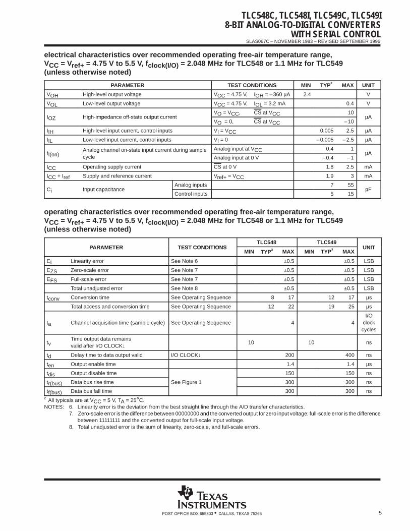
electrical characteristics over recommended operating free-air temperature range,VCC = Vref+ = 4.75 V to 5.5 V, f clock(I/O) = 2.048 MHz for TLC548 or 1.1 MHz for TLC549 (unless otherwise noted)
PARAMETER TEST CONDITIONS MIN TYP† MAX UNIT
VOH High-level output voltage VCC = 4.75 V, IOH = –360 µA 2.4 V
VOL Low-level output voltage VCC = 4.75 V, IOL = 3.2 mA 0.4 V
IOZ High impedance off state output currentVO = VCC, CS at VCC 10
µAIOZ High-impedance off-state output currentVO = 0, CS at VCC –10
µA
IIH High-level input current, control inputs VI = VCC 0.005 2.5 µA
IIL Low-level input current, control inputs VI = 0 –0.005 –2.5 µA
II( )Analog channel on-state input current during sample Analog input at VCC 0.4 1
µAII(on)g g
cycle Analog input at 0 V –0.4 –1µA
ICC Operating supply current CS at 0 V 1.8 2.5 mA
ICC + Iref Supply and reference current Vref+ = VCC 1.9 3 mA
Ci Input capacitanceAnalog inputs 7 55
pFCi Input capacitanceControl inputs 5 15
pF
operating characteristics over recommended operating free-air temperature range, VCC = Vref+ = 4.75 V to 5.5 V, f clock(I/O) = 2.048 MHz for TLC548 or 1.1 MHz for TLC549 (unless otherwise noted)
PARAMETER TEST CONDITIONSTLC548 TLC549
UNITPARAMETER TEST CONDITIONSMIN TYP† MAX MIN TYP† MAX
UNIT
EL Linearity error See Note 6 ±0.5 ±0.5 LSB
EZS Zero-scale error See Note 7 ±0.5 ±0.5 LSB
EFS Full-scale error See Note 7 ±0.5 ±0.5 LSB
Total unadjusted error See Note 8 ±0.5 ±0.5 LSB
tconv Conversion time See Operating Sequence 8 17 12 17 µs
Total access and conversion time See Operating Sequence 12 22 19 25 µs
ta Channel acquisition time (sample cycle) See Operating Sequence 4 4I/O
clockcycles
tvTime output data remainsvalid after I/O CLOCK↓ 10 10 ns
td Delay time to data output valid I/O CLOCK↓ 200 400 ns
ten Output enable time 1.4 1.4 µs
tdis Output disable time 150 150 ns
tr(bus) Data bus rise time See Figure 1 300 300 ns
tf(bus) Data bus fall time 300 300 ns† All typicals are at VCC = 5 V, TA = 25°C.NOTES: 6. Linearity error is the deviation from the best straight line through the A/D transfer characteristics.
7. Zero-scale error is the difference between 00000000 and the converted output for zero input voltage; full-scale error is the differencebetween 11111111 and the converted output for full-scale input voltage.
8. Total unadjusted error is the sum of linearity, zero-scale, and full-scale errors.
TLC548C, TLC548I, TLC549C, TLC549I8-BIT ANALOG-TO-DIGITAL CONVERTERSWITH SERIAL CONTROL
SLAS067C – NOVEMBER 1983 – REVISED SEPTEMBER 1996
6 POST OFFICE BOX 655303 • DALLAS, TEXAS 75265
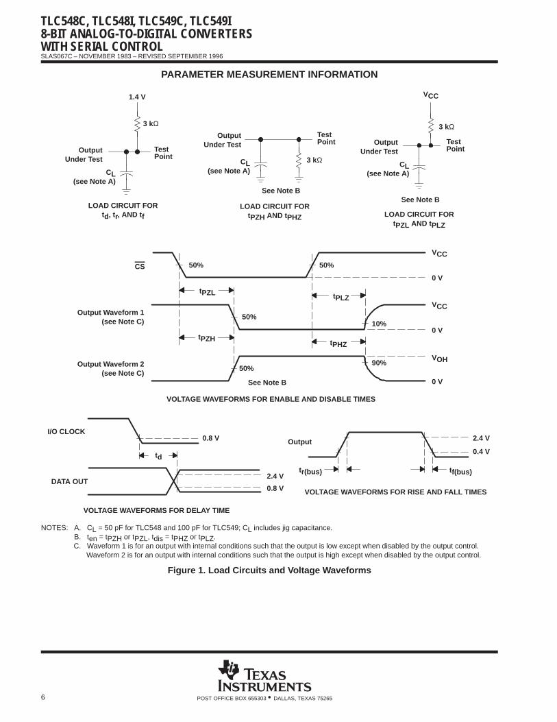
PARAMETER MEASUREMENT INFORMATION
See Note B
0.4 V
2.4 V
tf(bus)
Output
tr(bus)
0.8 V
2.4 V
0.8 V
td
DATA OUTVOLTAGE WAVEFORMS FOR RISE AND FALL TIMES
VOLTAGE WAVEFORMS FOR DELAY TIME
VCC
3 kΩ
3 kΩ
VCC
See Note B
50%
50%
0 V
0 V
tPLZ
I/O CLOCK
VOLTAGE WAVEFORMS FOR ENABLE AND DISABLE TIMES
Output Waveform 1(see Note C)
tPHZ
VOH90%
10%
tPZL
0 V
VCC
50%
CS
LOAD CIRCUIT FORtPZL AND tPLZ
LOAD CIRCUIT FORtPZH AND tPHZ
LOAD CIRCUIT FORtd, tr, AND t f
See Note B
OutputUnder Test
TestPoint
3 kΩ
1.4 V
Output Waveform 2(see Note C)
CL(see Note A)
OutputUnder Test
TestPoint
CL(see Note A)
OutputUnder Test
TestPoint
CL(see Note A)
tPZH
50%
NOTES: A. CL = 50 pF for TLC548 and 100 pF for TLC549; CL includes jig capacitance.B. ten = tPZH or tPZL, tdis = tPHZ or tPLZ.C. Waveform 1 is for an output with internal conditions such that the output is low except when disabled by the output control.
Waveform 2 is for an output with internal conditions such that the output is high except when disabled by the output control.
Figure 1. Load Circuits and Voltage Waveforms
TLC548C, TLC548I, TLC549C, TLC549I8-BIT ANALOG-TO-DIGITAL CONVERTERS
WITH SERIAL CONTROL
SLAS067C – NOVEMBER 1983 – REVISED SEPTEMBER 1996
7POST OFFICE BOX 655303 • DALLAS, TEXAS 75265
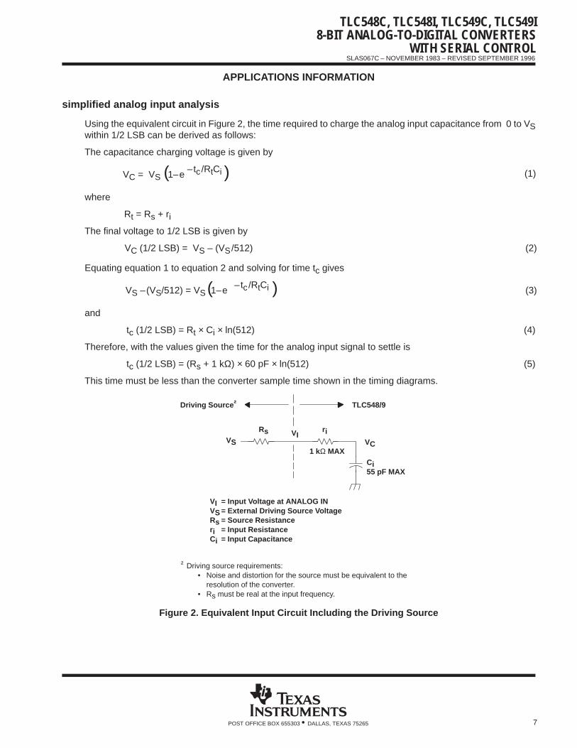
APPLICATIONS INFORMATION
simplified analog input analysis
Using the equivalent circuit in Figure 2, the time required to charge the analog input capacitance from 0 to VSwithin 1/2 LSB can be derived as follows:
The capacitance charging voltage is given by
VC = VS 1–e –tc/RtCi( ) (1)
where
Rt = Rs + ri
The final voltage to 1/2 LSB is given by
(2)VC (1/2 LSB) = VS – (VS/512)
Equating equation 1 to equation 2 and solving for time tc gives
VS –(VS/512) = VS 1–e (3)–tc /RtCi( )and
tc (1/2 LSB) = Rt × Ci × ln(512) (4)
Therefore, with the values given the time for the analog input signal to settle is
tc (1/2 LSB) = (Rs + 1 kΩ) × 60 pF × ln(512) (5)
This time must be less than the converter sample time shown in the timing diagrams.
Rs riVS VC
1 kΩ MAX
Driving Source † TLC548/9
VI
VI = Input Voltage at ANALOG INVS = External Driving Source VoltageRs = Source Resistanceri = Input ResistanceCi = Input Capacitance
† Driving source requirements:• Noise and distortion for the source must be equivalent to the
resolution of the converter.• Rs must be real at the input frequency.
Ci55 pF MAX
Figure 2. Equivalent Input Circuit Including the Driving Source
TLC548C, TLC548I, TLC549C, TLC549I8-BIT ANALOG-TO-DIGITAL CONVERTERSWITH SERIAL CONTROL
SLAS067C – NOVEMBER 1983 – REVISED SEPTEMBER 1996
8 POST OFFICE BOX 655303 • DALLAS, TEXAS 75265
PRINCIPLES OF OPERATION
The TLC548 and TLC549 are each complete data acquisition systems on a single chip. Each contains an internalsystem clock, sample-and-hold function, 8-bit A/D converter, data register, and control logic circuitry. For flexibilityand access speed, there are two control inputs: I/O CLOCK and chip select (CS). These control inputs and aTTL-compatible 3-state output facilitate serial communications with a microprocessor or minicomputer. A conversioncan be completed in 17 µs or less, while complete input-conversion-output cycles can be repeated in 22 µs for theTLC548 and in 25 µs for the TLC549.
The internal system clock and I/O CLOCK are used independently and do not require any special speed or phaserelationships between them. This independence simplifies the hardware and software control tasks for the device.Due to this independence and the internal generation of the system clock, the control hardware and software needonly be concerned with reading the previous conversion result and starting the conversion by using the I/O clock. Inthis manner, the internal system clock drives the “conversion crunching” circuitry so that the control hardware andsoftware need not be concerned with this task.
When CS is high, DATA OUT is in a high-impedance condition and I/O CLOCK is disabled. This CS control functionallows I/O CLOCK to share the same control logic point with its counterpart terminal when additional TLC548 andTLC549 devices are used. This also serves to minimize the required control logic terminals when using multipleTLC548 and TLC549 devices.
The control sequence has been designed to minimize the time and effort required to initiate conversion and obtainthe conversion result. A normal control sequence is:
1. CS is brought low. To minimize errors caused by noise at CS, the internal circuitry waits for two rising edgesand then a falling edge of the internal system clock after a CS↓ before the transition is recognized. However,upon a CS rising edge, DATA OUT goes to a high-impedance state within the specified tdis even though therest of the integrated circuitry does not recognize the transition until the specified tsu(CS) has elapsed. Thistechnique protects the device against noise when used in a noisy environment. The most significant bit (MSB)of the previous conversion result initially appears on DATA OUT when CS goes low.
2. The falling edges of the first four I/O CLOCK cycles shift out the second, third, fourth, and fifth most significantbits of the previous conversion result. The on-chip sample-and-hold function begins sampling the analoginput after the fourth high-to-low transition of I/O CLOCK. The sampling operation basically involves thecharging of internal capacitors to the level of the analog input voltage.
3. Three more I/O CLOCK cycles are then applied to the I/O CLOCK terminal and the sixth, seventh, and eighthconversion bits are shifted out on the falling edges of these clock cycles.
4. The final (the eighth) clock cycle is applied to I/O CLOCK. The on-chip sample-and-hold function begins thehold operation upon the high-to-low transition of this clock cycle. The hold function continues for the next fourinternal system clock cycles, after which the holding function terminates and the conversion is performedduring the next 32 system clock cycles, giving a total of 36 cycles. After the eighth I/O CLOCK cycle, CS mustgo high or the I/O clock must remain low for at least 36 internal system clock cycles to allow for the completionof the hold and conversion functions. CS can be kept low during periods of multiple conversion. Whenkeeping CS low during periods of multiple conversion, special care must be exercised to prevent noiseglitches on the I/O CLOCK line. If glitches occur on I/O CLOCK, the I/O sequence between themicroprocessor/controller and the device loses synchronization. When CS is taken high, it must remain highuntil the end of conversion. Otherwise, a valid high-to-low transition of CS causes a reset condition, whichaborts the conversion in progress.
A new conversion may be started and the ongoing conversion simultaneously aborted by performing steps 1 through4 before the 36 internal system clock cycles occur. Such action yields the conversion result of the previous conversionand not the ongoing conversion.
TLC548C, TLC548I, TLC549C, TLC549I8-BIT ANALOG-TO-DIGITAL CONVERTERS
WITH SERIAL CONTROL
SLAS067C – NOVEMBER 1983 – REVISED SEPTEMBER 1996
9POST OFFICE BOX 655303 • DALLAS, TEXAS 75265
PRINCIPLES OF OPERATION
For certain applications, such as strobing applications, it is necessary to start conversion at a specific point in time.This device accommodates these applications. Although the on-chip sample-and-hold function begins samplingupon the high-to-low transition of the fourth I/O CLOCK cycle, the hold function does not begin until the high-to-lowtransition of the eighth I/O CLOCK cycle, which should occur at the moment when the analog signal must beconverted. The TLC548 and TLC549 continue sampling the analog input until the high-to-low transition of the eighthI/O CLOCK pulse. The control circuitry or software then immediately lowers I/O CLOCK and starts the holding functionto hold the analog signal at the desired point in time and starts the conversion.
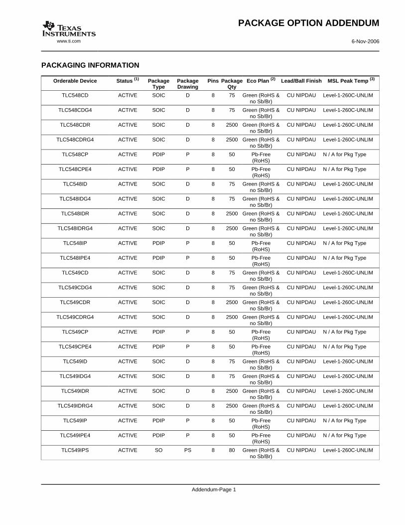
PACKAGING INFORMATION
Orderable Device Status (1) PackageType
PackageDrawing
Pins PackageQty
Eco Plan (2) Lead/Ball Finish MSL Peak Temp (3)
TLC548CD ACTIVE SOIC D 8 75 Green (RoHS &no Sb/Br)
CU NIPDAU Level-1-260C-UNLIM
TLC548CDG4 ACTIVE SOIC D 8 75 Green (RoHS &no Sb/Br)
CU NIPDAU Level-1-260C-UNLIM
TLC548CDR ACTIVE SOIC D 8 2500 Green (RoHS &no Sb/Br)
CU NIPDAU Level-1-260C-UNLIM
TLC548CDRG4 ACTIVE SOIC D 8 2500 Green (RoHS &no Sb/Br)
CU NIPDAU Level-1-260C-UNLIM
TLC548CP ACTIVE PDIP P 8 50 Pb-Free(RoHS)
CU NIPDAU N / A for Pkg Type
TLC548CPE4 ACTIVE PDIP P 8 50 Pb-Free(RoHS)
CU NIPDAU N / A for Pkg Type
TLC548ID ACTIVE SOIC D 8 75 Green (RoHS &no Sb/Br)
CU NIPDAU Level-1-260C-UNLIM
TLC548IDG4 ACTIVE SOIC D 8 75 Green (RoHS &no Sb/Br)
CU NIPDAU Level-1-260C-UNLIM
TLC548IDR ACTIVE SOIC D 8 2500 Green (RoHS &no Sb/Br)
CU NIPDAU Level-1-260C-UNLIM
TLC548IDRG4 ACTIVE SOIC D 8 2500 Green (RoHS &no Sb/Br)
CU NIPDAU Level-1-260C-UNLIM
TLC548IP ACTIVE PDIP P 8 50 Pb-Free(RoHS)
CU NIPDAU N / A for Pkg Type
TLC548IPE4 ACTIVE PDIP P 8 50 Pb-Free(RoHS)
CU NIPDAU N / A for Pkg Type
TLC549CD ACTIVE SOIC D 8 75 Green (RoHS &no Sb/Br)
CU NIPDAU Level-1-260C-UNLIM
TLC549CDG4 ACTIVE SOIC D 8 75 Green (RoHS &no Sb/Br)
CU NIPDAU Level-1-260C-UNLIM
TLC549CDR ACTIVE SOIC D 8 2500 Green (RoHS &no Sb/Br)
CU NIPDAU Level-1-260C-UNLIM
TLC549CDRG4 ACTIVE SOIC D 8 2500 Green (RoHS &no Sb/Br)
CU NIPDAU Level-1-260C-UNLIM
TLC549CP ACTIVE PDIP P 8 50 Pb-Free(RoHS)
CU NIPDAU N / A for Pkg Type
TLC549CPE4 ACTIVE PDIP P 8 50 Pb-Free(RoHS)
CU NIPDAU N / A for Pkg Type
TLC549ID ACTIVE SOIC D 8 75 Green (RoHS &no Sb/Br)
CU NIPDAU Level-1-260C-UNLIM
TLC549IDG4 ACTIVE SOIC D 8 75 Green (RoHS &no Sb/Br)
CU NIPDAU Level-1-260C-UNLIM
TLC549IDR ACTIVE SOIC D 8 2500 Green (RoHS &no Sb/Br)
CU NIPDAU Level-1-260C-UNLIM
TLC549IDRG4 ACTIVE SOIC D 8 2500 Green (RoHS &no Sb/Br)
CU NIPDAU Level-1-260C-UNLIM
TLC549IP ACTIVE PDIP P 8 50 Pb-Free(RoHS)
CU NIPDAU N / A for Pkg Type
TLC549IPE4 ACTIVE PDIP P 8 50 Pb-Free(RoHS)
CU NIPDAU N / A for Pkg Type
TLC549IPS ACTIVE SO PS 8 80 Green (RoHS &no Sb/Br)
CU NIPDAU Level-1-260C-UNLIM
PACKAGE OPTION ADDENDUM
www.ti.com 6-Nov-2006
Addendum-Page 1
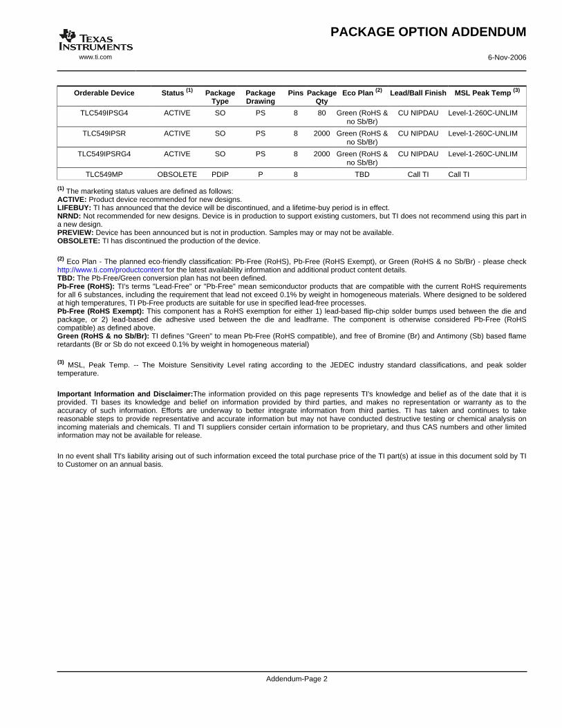
Orderable Device Status (1) PackageType
PackageDrawing
Pins PackageQty
Eco Plan (2) Lead/Ball Finish MSL Peak Temp (3)
TLC549IPSG4 ACTIVE SO PS 8 80 Green (RoHS &no Sb/Br)
CU NIPDAU Level-1-260C-UNLIM
TLC549IPSR ACTIVE SO PS 8 2000 Green (RoHS &no Sb/Br)
CU NIPDAU Level-1-260C-UNLIM
TLC549IPSRG4 ACTIVE SO PS 8 2000 Green (RoHS &no Sb/Br)
CU NIPDAU Level-1-260C-UNLIM
TLC549MP OBSOLETE PDIP P 8 TBD Call TI Call TI
(1) The marketing status values are defined as follows:ACTIVE: Product device recommended for new designs.LIFEBUY: TI has announced that the device will be discontinued, and a lifetime-buy period is in effect.NRND: Not recommended for new designs. Device is in production to support existing customers, but TI does not recommend using this part ina new design.PREVIEW: Device has been announced but is not in production. Samples may or may not be available.OBSOLETE: TI has discontinued the production of the device.
(2) Eco Plan - The planned eco-friendly classification: Pb-Free (RoHS), Pb-Free (RoHS Exempt), or Green (RoHS & no Sb/Br) - please checkhttp://www.ti.com/productcontent for the latest availability information and additional product content details.TBD: The Pb-Free/Green conversion plan has not been defined.Pb-Free (RoHS): TI's terms "Lead-Free" or "Pb-Free" mean semiconductor products that are compatible with the current RoHS requirementsfor all 6 substances, including the requirement that lead not exceed 0.1% by weight in homogeneous materials. Where designed to be solderedat high temperatures, TI Pb-Free products are suitable for use in specified lead-free processes.Pb-Free (RoHS Exempt): This component has a RoHS exemption for either 1) lead-based flip-chip solder bumps used between the die andpackage, or 2) lead-based die adhesive used between the die and leadframe. The component is otherwise considered Pb-Free (RoHScompatible) as defined above.Green (RoHS & no Sb/Br): TI defines "Green" to mean Pb-Free (RoHS compatible), and free of Bromine (Br) and Antimony (Sb) based flameretardants (Br or Sb do not exceed 0.1% by weight in homogeneous material)
(3) MSL, Peak Temp. -- The Moisture Sensitivity Level rating according to the JEDEC industry standard classifications, and peak soldertemperature.
Important Information and Disclaimer:The information provided on this page represents TI's knowledge and belief as of the date that it isprovided. TI bases its knowledge and belief on information provided by third parties, and makes no representation or warranty as to theaccuracy of such information. Efforts are underway to better integrate information from third parties. TI has taken and continues to takereasonable steps to provide representative and accurate information but may not have conducted destructive testing or chemical analysis onincoming materials and chemicals. TI and TI suppliers consider certain information to be proprietary, and thus CAS numbers and other limitedinformation may not be available for release.
In no event shall TI's liability arising out of such information exceed the total purchase price of the TI part(s) at issue in this document sold by TIto Customer on an annual basis.
PACKAGE OPTION ADDENDUM
www.ti.com 6-Nov-2006
Addendum-Page 2
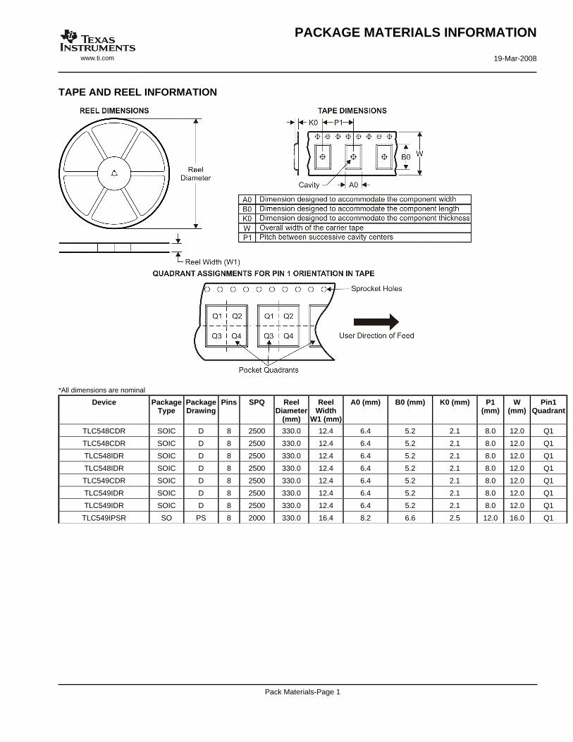
TAPE AND REEL INFORMATION
*All dimensions are nominal
Device PackageType
PackageDrawing
Pins SPQ ReelDiameter
(mm)
ReelWidth
W1 (mm)
A0 (mm) B0 (mm) K0 (mm) P1(mm)
W(mm)
Pin1Quadrant
TLC548CDR SOIC D 8 2500 330.0 12.4 6.4 5.2 2.1 8.0 12.0 Q1
TLC548CDR SOIC D 8 2500 330.0 12.4 6.4 5.2 2.1 8.0 12.0 Q1
TLC548IDR SOIC D 8 2500 330.0 12.4 6.4 5.2 2.1 8.0 12.0 Q1
TLC548IDR SOIC D 8 2500 330.0 12.4 6.4 5.2 2.1 8.0 12.0 Q1
TLC549CDR SOIC D 8 2500 330.0 12.4 6.4 5.2 2.1 8.0 12.0 Q1
TLC549IDR SOIC D 8 2500 330.0 12.4 6.4 5.2 2.1 8.0 12.0 Q1
TLC549IDR SOIC D 8 2500 330.0 12.4 6.4 5.2 2.1 8.0 12.0 Q1
TLC549IPSR SO PS 8 2000 330.0 16.4 8.2 6.6 2.5 12.0 16.0 Q1
PACKAGE MATERIALS INFORMATION
www.ti.com 19-Mar-2008
Pack Materials-Page 1
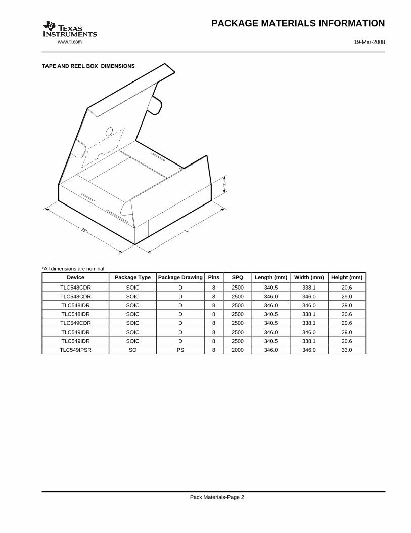
*All dimensions are nominal
Device Package Type Package Drawing Pins SPQ Length (mm) Width (mm) Height (mm)
TLC548CDR SOIC D 8 2500 340.5 338.1 20.6
TLC548CDR SOIC D 8 2500 346.0 346.0 29.0
TLC548IDR SOIC D 8 2500 346.0 346.0 29.0
TLC548IDR SOIC D 8 2500 340.5 338.1 20.6
TLC549CDR SOIC D 8 2500 340.5 338.1 20.6
TLC549IDR SOIC D 8 2500 346.0 346.0 29.0
TLC549IDR SOIC D 8 2500 340.5 338.1 20.6
TLC549IPSR SO PS 8 2000 346.0 346.0 33.0
PACKAGE MATERIALS INFORMATION
www.ti.com 19-Mar-2008
Pack Materials-Page 2
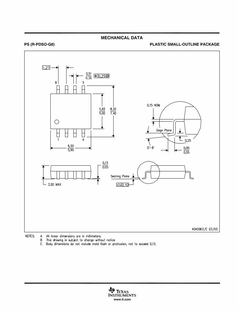
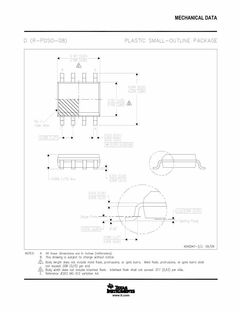
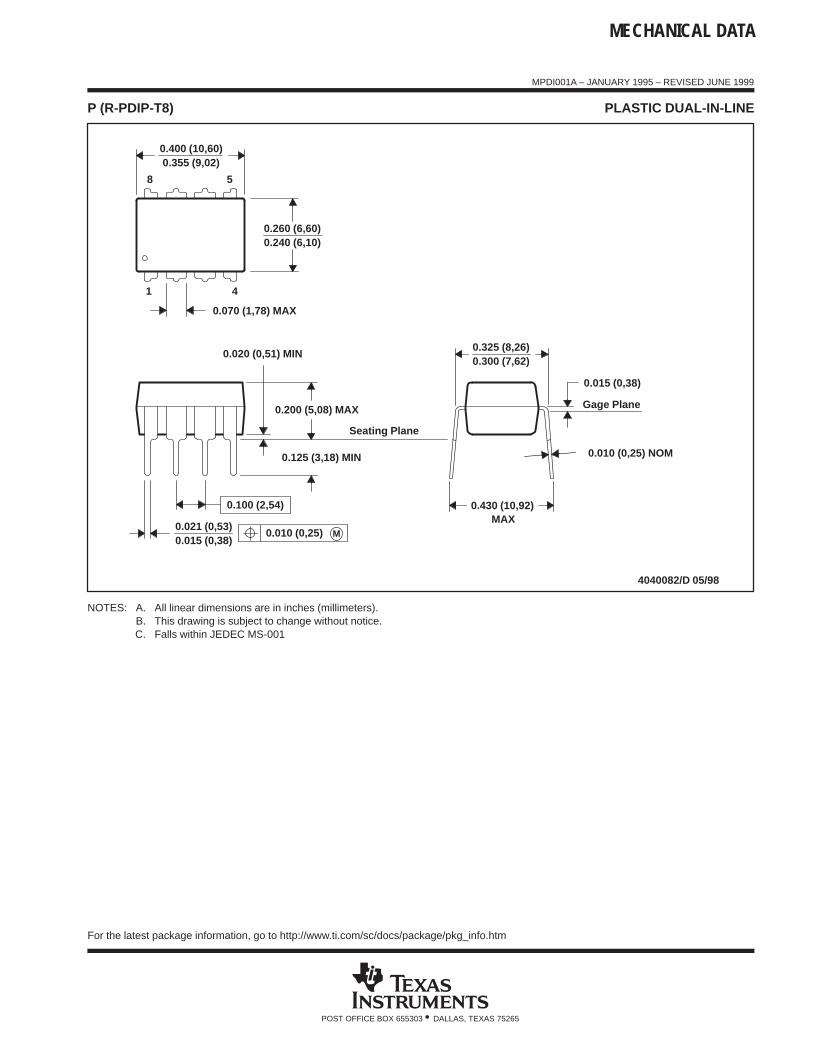
MECHANICAL DATA
MPDI001A – JANUARY 1995 – REVISED JUNE 1999
POST OFFICE BOX 655303 • DALLAS, TEXAS 75265
P (R-PDIP-T8) PLASTIC DUAL-IN-LINE
8
4
0.015 (0,38)
Gage Plane
0.325 (8,26)0.300 (7,62)
0.010 (0,25) NOM
MAX0.430 (10,92)
4040082/D 05/98
0.200 (5,08) MAX
0.125 (3,18) MIN
5
0.355 (9,02)
0.020 (0,51) MIN
0.070 (1,78) MAX
0.240 (6,10)0.260 (6,60)
0.400 (10,60)
1
0.015 (0,38)0.021 (0,53)
Seating Plane
M0.010 (0,25)
0.100 (2,54)
NOTES: A. All linear dimensions are in inches (millimeters).B. This drawing is subject to change without notice.C. Falls within JEDEC MS-001
For the latest package information, go to http://www.ti.com/sc/docs/package/pkg_info.htm
IMPORTANT NOTICETexas Instruments Incorporated and its subsidiaries (TI) reserve the right to make corrections, modifications, enhancements, improvements,and other changes to its products and services at any time and to discontinue any product or service without notice. Customers shouldobtain the latest relevant information before placing orders and should verify that such information is current and complete. All products aresold subject to TI’s terms and conditions of sale supplied at the time of order acknowledgment.TI warrants performance of its hardware products to the specifications applicable at the time of sale in accordance with TI’s standardwarranty. Testing and other quality control techniques are used to the extent TI deems necessary to support this warranty. Except wheremandated by government requirements, testing of all parameters of each product is not necessarily performed.TI assumes no liability for applications assistance or customer product design. Customers are responsible for their products andapplications using TI components. To minimize the risks associated with customer products and applications, customers should provideadequate design and operating safeguards.TI does not warrant or represent that any license, either express or implied, is granted under any TI patent right, copyright, mask work right,or other TI intellectual property right relating to any combination, machine, or process in which TI products or services are used. Informationpublished by TI regarding third-party products or services does not constitute a license from TI to use such products or services or awarranty or endorsement thereof. Use of such information may require a license from a third party under the patents or other intellectualproperty of the third party, or a license from TI under the patents or other intellectual property of TI.Reproduction of TI information in TI data books or data sheets is permissible only if reproduction is without alteration and is accompaniedby all associated warranties, conditions, limitations, and notices. Reproduction of this information with alteration is an unfair and deceptivebusiness practice. TI is not responsible or liable for such altered documentation. Information of third parties may be subject to additionalrestrictions.Resale of TI products or services with statements different from or beyond the parameters stated by TI for that product or service voids allexpress and any implied warranties for the associated TI product or service and is an unfair and deceptive business practice. TI is notresponsible or liable for any such statements.TI products are not authorized for use in safety-critical applications (such as life support) where a failure of the TI product would reasonablybe expected to cause severe personal injury or death, unless officers of the parties have executed an agreement specifically governingsuch use. Buyers represent that they have all necessary expertise in the safety and regulatory ramifications of their applications, andacknowledge and agree that they are solely responsible for all legal, regulatory and safety-related requirements concerning their productsand any use of TI products in such safety-critical applications, notwithstanding any applications-related information or support that may beprovided by TI. Further, Buyers must fully indemnify TI and its representatives against any damages arising out of the use of TI products insuch safety-critical applications.TI products are neither designed nor intended for use in military/aerospace applications or environments unless the TI products arespecifically designated by TI as military-grade or "enhanced plastic." Only products designated by TI as military-grade meet militaryspecifications. Buyers acknowledge and agree that any such use of TI products which TI has not designated as military-grade is solely atthe Buyer's risk, and that they are solely responsible for compliance with all legal and regulatory requirements in connection with such use.TI products are neither designed nor intended for use in automotive applications or environments unless the specific TI products aredesignated by TI as compliant with ISO/TS 16949 requirements. Buyers acknowledge and agree that, if they use any non-designatedproducts in automotive applications, TI will not be responsible for any failure to meet such requirements.Following are URLs where you can obtain information on other Texas Instruments products and application solutions:Products ApplicationsAmplifiers amplifier.ti.com Audio www.ti.com/audioData Converters dataconverter.ti.com Automotive www.ti.com/automotiveDLP® Products www.dlp.com Broadband www.ti.com/broadbandDSP dsp.ti.com Digital Control www.ti.com/digitalcontrolClocks and Timers www.ti.com/clocks Medical www.ti.com/medicalInterface interface.ti.com Military www.ti.com/militaryLogic logic.ti.com Optical Networking www.ti.com/opticalnetworkPower Mgmt power.ti.com Security www.ti.com/securityMicrocontrollers microcontroller.ti.com Telephony www.ti.com/telephonyRFID www.ti-rfid.com Video & Imaging www.ti.com/videoRF/IF and ZigBee® Solutions www.ti.com/lprf Wireless www.ti.com/wireless
Mailing Address: Texas Instruments, Post Office Box 655303, Dallas, Texas 75265Copyright © 2009, Texas Instruments Incorporated