Embed Size (px)
Citation preview
AVAILABLE
Functional Diagrams
Pin Configurations appear at end of data sheet.Functional Diagrams continued at end of data sheet.UCSP is a trademark of Maxim Integrated Products, Inc.
For pricing, delivery, and ordering information, please contact Maxim Direct at 1-888-629-4642, or visit Maxim’s website at www.maximintegrated.com.
19-6039; Rev 2; 4/12
78M66313-Phase Power-Measurement IC
DATA SHEET
DS_6631_056
DESCRIPTION The Teridian™ 78M6631 is a highly integrated 3-phase power measurement and monitoring system-on-chip (SoC), with a 10 MHz 8051-compatible MPU core and Single Converter Technology® containing a 22-bit delta-sigma converter and 32-bit compute engine (CE). The 78M6631 has been designed specifically for a wide variety of applications requiring 3-phase power and quality measurements. It supports both Delta and Wye configurations.
At the measurement interface, the device provides six analog inputs including three differential current and three voltage for interfacing to current and voltage sensors. The device provides better than 0.5% accuracy over a wide 2000:1 dynamic range.
The integrated MPU core and 128 KB of flash memory provide a flexible means of configuration, post-processing, data formatting, interfacing to host processor via a UART or SPI interface, or using DIO pins for LEDs or relay control. Complete firmware is available from Maxim and can be loaded into the IC during manufacturing test.
FEATURES < 0.5% Watt Accuracy Over 2000:1 Current
Range and Over Temperature Exceeds IEC 62053/ANSI C12.20 Standards Voltage Reference < 40 ppm/°C
Six Analog Inputs Supporting 3-Phase Voltage and Current Measurement Inputs
Pin- or Biselectable Delta or Wye Configuration
22-Bit Delta-Sigma ADC with Independent 32-Bit Compute Engine (CE)
8-Bit MPU (80515), One Clock Cycle per Instruction with 4 KB MPU XRAM
128 KB Flash with Security
32 kHz Time Base with Hardware Watchdog Timer
UART, I2C, and High-Speed Slave SPI Host Interface Options
17 General-Purpose 5 V Tolerant I/O Pins
Packaged in a RoHS-Compliant (6/6) Lead(Pb)-Free 56-Pin TQFN
Application Firmware Includes (per Phase): o True RMS Current and Voltage Calculations o Active, Reactive, Apparent, Fundamental,
and Harmonic Power Calculations o Fundamental and Harmonic Current and
Voltage Calculations o Line Frequency and Power Factor
Calculations
o Phase Compensation (18 at 60 Hz)
o Built-In Calibration Routines o Programmable Alarm Thresholds o Command Line (UART) Communications
o High-Speed SPI Communications
Teridian is a trademark and Single Converter Technology is a registered trademark of Maxim Integrated Products, Inc.
78M6631 Data Sheet DS_6631_056
Table of Contents
1 Hardware Functional Description......................................................................................................5 1.1 Hardware Overview .....................................................................................................................5 1.2 Device Reset................................................................................................................................7 1.3 Power Management.....................................................................................................................7
1.3.1 Voltage Regulator ............................................................................................................7 1.3.2 Power Fault Management................................................................................................7
1.4 Analog Front-End (AFE) ..............................................................................................................8 1.4.1 Analog Current and Voltage Inputs .................................................................................8
1.5 Digital Computation Engine (CE).................................................................................................9 1.6 80515 MPU Core .......................................................................................................................10
1.6.1 SFRs ..............................................................................................................................10 1.7 RAM ...........................................................................................................................................10 1.8 IORAM .......................................................................................................................................10 1.9 Flash ..........................................................................................................................................10
1.9.1 Program Security ...........................................................................................................10 1.10 Oscillator ....................................................................................................................................11 1.11 PLL and Internal Clock Generation............................................................................................11 1.12 Real-Time Clock (RTC)..............................................................................................................11 1.13 Hardware Watchdog Timer........................................................................................................11 1.14 Temperature Sensor ..................................................................................................................12 1.15 General Purpose Digital I/O.......................................................................................................12 1.16 D/Y Selection Pin .......................................................................................................................12 1.17 EEPROM Interface ....................................................................................................................12 1.18 SPI Slave Port............................................................................................................................12 1.19 Test Port.....................................................................................................................................13 1.20 UART .........................................................................................................................................13 1.21 In Circuit Emulator (ICE) Port ....................................................................................................14
2 Electrical Specifications...................................................................................................................15 2.1 Absolute Maximum Ratings .......................................................................................................15 2.2 Recommended External Components.......................................................................................16 2.3 Recommended Operating Conditions........................................................................................16 2.4 Performance Specifications .......................................................................................................17
2.4.1 Input Logic Levels..........................................................................................................17 2.4.2 Output Logic Levels .......................................................................................................17 2.4.3 Power-Fault Comparator ...............................................................................................17 2.4.4 Power Supply Monitor....................................................................................................18 2.4.5 Supply Current ...............................................................................................................18 2.4.6 Crystal Oscillator............................................................................................................18 2.4.7 Temperature Sensor......................................................................................................19 2.4.8 VREF .............................................................................................................................19 2.4.9 ADC Converter, V3P3A Referenced .............................................................................20
2.5 Timing Specifications .................................................................................................................21 2.5.1 Flash Memory ................................................................................................................21 2.5.2 EEPROM Interface ........................................................................................................21 2.5.3 RESET...........................................................................................................................21 2.5.4 SPI Slave Port................................................................................................................22
3 Packaging ..........................................................................................................................................23 3.1 56-Pin QFN Package.................................................................................................................23 3.2 Pinout .........................................................................................................................................23
3.2.1 56-Pin QFN Package Outline ........................................................................................24 3.2.2 Recommended PCB Land Pattern for the QFN-56 Package ........................................25
4 Pin Descriptions................................................................................................................................26
2 Rev 2
DS_6631_056 78M6631 Data Sheet
4.1 Power and Ground Pins.............................................................................................................26 4.2 Analog Pins................................................................................................................................26 4.3 Digital Pins .................................................................................................................................27
5 I/O Equivalent Circuits......................................................................................................................28 6 Ordering Information ........................................................................................................................29 7 Contact Information..........................................................................................................................29 Revision History........................................................................................................................................30
Rev 2 3
78M6631 Data Sheet DS_6631_056
Figures Figure 1: 78M6631 IC Functional Block Diagram .........................................................................................6 Figure 2: AFE Block Diagram .......................................................................................................................8 Figure 3: Functions Defined by V1..............................................................................................................11 Figure 4: SPI Slave Port: Typical Read and Write Operations ...................................................................13 Figure 5: SPI Slave Port Timing..................................................................................................................22 Figure 6: Pinout for QFN-56 Package.........................................................................................................23 Figure 7: PCB Land Pattern for QFN-56 Package......................................................................................25 Figure 8: I/O Equivalent Circuits .................................................................................................................28 Tables Table 1: SPI Command Description............................................................................................................13 Table 2: Absolute Maximum Ratings ..........................................................................................................15 Table 3: Recommended External Components ..........................................................................................16 Table 4: Recommended Operating Conditions...........................................................................................16 Table 5: Input Logic Levels .........................................................................................................................17 Table 6: Output Logic Levels ......................................................................................................................17 Table 7: Power-Fault Comparator Performance Specifications..................................................................17 Table 8: Power Supply Monitor Performance Specifications (BME= 1)......................................................18 Table 9: Supply Current Performance Specifications .................................................................................18 Table 10: Crystal Oscillator Performance Specifications............................................................................18 Table 11: Temperature Sensor Performance Specifications ......................................................................19 Table 12: VREF Performance Specifications..............................................................................................19 Table 13: ADC Converter Performance Specifications...............................................................................20 Table 14: Flash Memory Timing Specifications ..........................................................................................21 Table 15: EEPROM Interface Timing..........................................................................................................21 Table 16: RESET Timing ............................................................................................................................21 Table 17: SPI Slave Port Timing.................................................................................................................22 Table 19: Power and Ground Pins..............................................................................................................26 Table 20: Analog Pins .................................................................................................................................26 Table 21: Digital Pins ..................................................................................................................................27 Table 22: Ordering Information ...................................................................................................................29
4 Rev 2
DS_6631_056 78M6631 Data Sheet
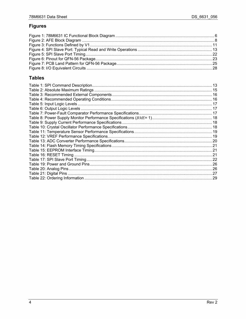
1 Hardware Functional Description 1.1 Hardware Overview The Teridian 78M6631 single-chip power measurement and monitoring device integrates all the primary AC measurement and control blocks required to implement the 3-phase power measurement and monitoring system. The 78M6631 includes:
Six input analog front-end (AFE) (3 Differential Current/3 Voltage)
Independent digital computation engine (CE)
8051-compatible microprocessor (MPU) which executes one instruction per clock cycle (80515)
Precision voltage reference
Temperature sensor
RAM and flash memory
A variety of I/O pins Communication Interfaces: UART, SPI, and I2C (Master) Various current sensor technologies are supported including Current Transformers (CT), Resistive Shunts, and Rogowski coils. The 32-bit compute engine (CE) of the 78M6631 sequentially process the samples from the analog inputs on pins IA, IB, IC, VA, VB, and VC and performs calculations to measure active power (Watts), reactive power (VARs), apparent power (VAs), power factor, fundamental power, and harmonic power for three independent phases. RMS, fundamental, and harmonic currents and voltages are also computed for each phase. Totals are available for most results. Figure 1 provides a block diagram of the 78M6631 IC. A detailed description of the various functional blocks follows. Refer to the applicable Firmware Description Document for additional supported functionality.
Rev 2 5
78M6631 Data Sheet DS_6631_056
ADCCONVERTER
VREFMUXP
XIN
XOUT
VREF
RESET
V1
UART
TX
RXDIGITAL I/O
POWER FAULT
GNDD
V3P3A
V3P3D
VOLTREG
2.5V to Logic
TMUXOUT
FAULTZ
GNDA
VBIAS
TEMP
OSC(32.768kHz)
MCKPLL
VREF
CKTEST TEST MODE
E_ RXTX
RTC
VBIAS
ICE_E
TESTMUX
V3P3D
CE_ PROG
CK_CE
CK_MPU80MHz
VADC
CE
MULTI-PURPOSE
IO
RTM
RPULSE
WPULSE
DIO_4...
to TMUX
SPI SLAVE
EEPROM I/F
FLASH128KB
XRAM4kB
CE_ DATA
PCSZPCLK
PSDIPSDO
SDATA
SDCK
SFR
80515MPU
EMULATORE_ TCLK
E_ RSTZ
E_ RXTXE_ TCLKE_RST
RP
ULS
EW
PU
LS
E
XRAM BUS
8
1632
CKTEST
ICE_E
CKTESTI
PCLKPSDOPCSZPSDI
FIR
VB
VC
VA XPULSE
YPULSE
XP
ULS
EY
PU
LSE
IBN
ICP
ICN
IBP
IAP
IAN
DIO3DIO4/SDCKDIO5/SDATADIO6DIO8DIO9D/YDIO11
DIO17
DIO24DIO25
DIO45DIO47
V3P3SYS
VBAT
DIO51DIO53
DIO30
DIO55
DIO29
Figure 1: 78M6631 IC Functional Block Diagram
6 Rev 2
DS_6631_056 78M6631 Data Sheet
1.2 Device Reset When the RESET pin is pulled high, all digital activity stops. Only the oscillator and RTC module continue to run. Additionally, all IORAM bits are set to their default states. As long as V1 (the input voltage at the power fault block) is greater than VBIAS, the internal 2.5 V regulator continues to provide power to the digital section. Once initiated, the reset mode persists until the reset timer times out. This occurs in 4096 cycles of the crystal clock after RESET goes low, at which time the MPU begins executing its preboot and boot sequences from address 0x0000. 1.3 Power Management 1.3.1 Voltage Regulator The 78M6631 provides an on-chip voltage regulator to create a 2.5 V supply for the digital logic. This regulator can be run off of the V3P3SYS or VBAT inputs depending upon power availability. 1.3.2 Power Fault Management The 78M6631 provides for both hardware and software controlled power fault management. The V1 pin is connected to a comparator to monitor system power fault conditions. When the input to the comparator falls (V1 < VBIAS) the device can enter a BROWNOUT mode, if supported in firmware and there is sufficient voltage on VBAT, that reduces the MPU rate to 32 kHz and disables all the measurement front-end circuits. If the overhead on VBAT is insufficient to maintain a BROWNOUT mode, then the device can also attempt to enter a SLEEP mode where only RTC functions are active. If there is not sufficient voltage on VBAT (or it is not supported), then the part enters RESET mode when the comparator fails.
Rev 2 7
78M6631 Data Sheet DS_6631_056
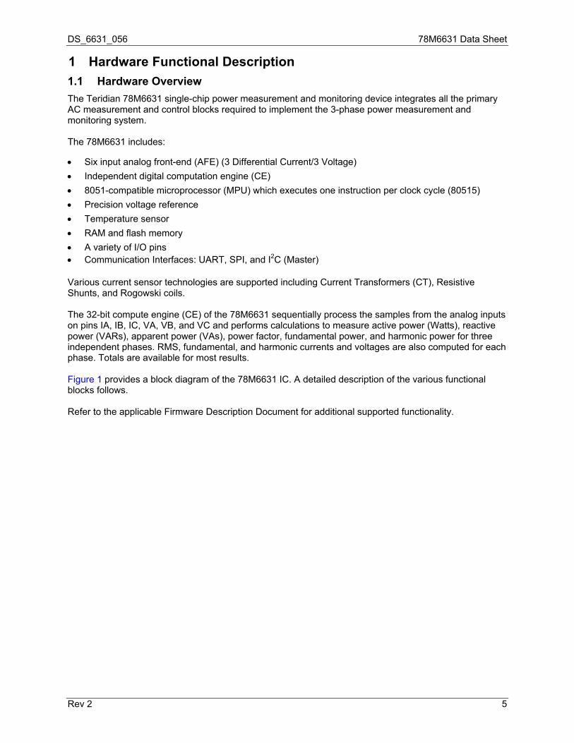
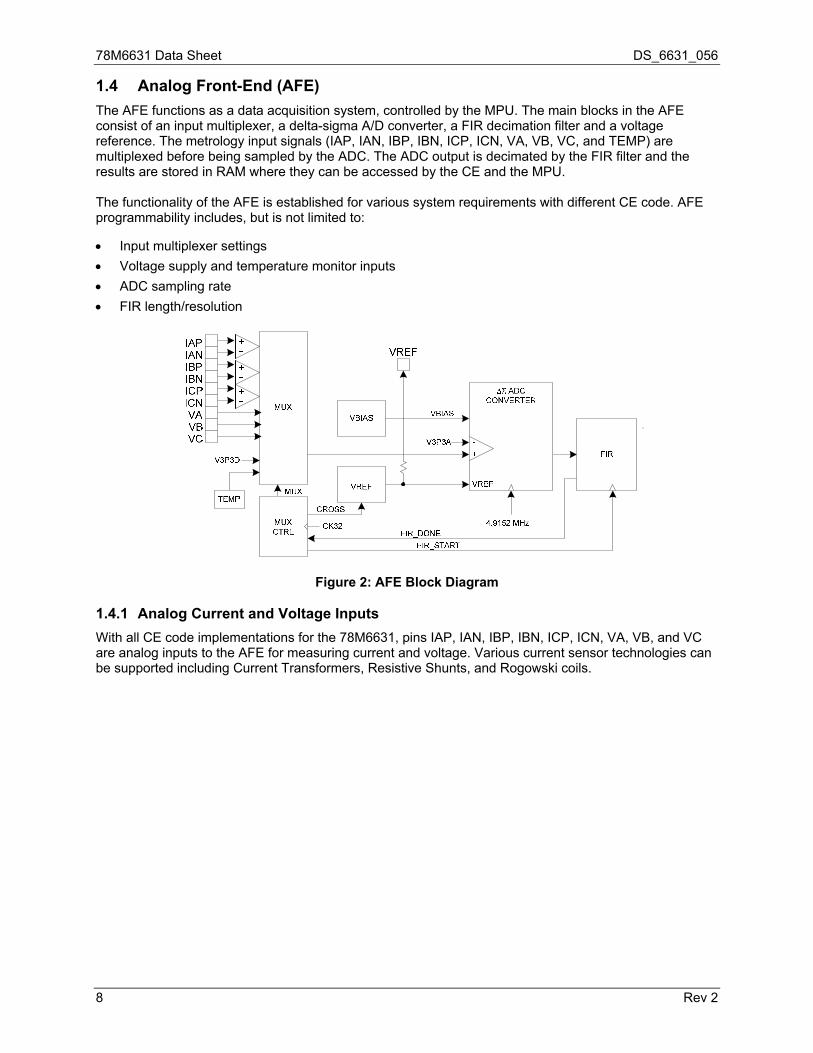
1.4 Analog Front-End (AFE) The AFE functions as a data acquisition system, controlled by the MPU. The main blocks in the AFE consist of an input multiplexer, a delta-sigma A/D converter, a FIR decimation filter and a voltage reference. The metrology input signals (IAP, IAN, IBP, IBN, ICP, ICN, VA, VB, VC, and TEMP) are multiplexed before being sampled by the ADC. The ADC output is decimated by the FIR filter and the results are stored in RAM where they can be accessed by the CE and the MPU. The functionality of the AFE is established for various system requirements with different CE code. AFE programmability includes, but is not limited to:
Input multiplexer settings
Voltage supply and temperature monitor inputs
ADC sampling rate
FIR length/resolution
Figure 2: AFE Block Diagram 1.4.1 Analog Current and Voltage Inputs With all CE code implementations for the 78M6631, pins IAP, IAN, IBP, IBN, ICP, ICN, VA, VB, and VC are analog inputs to the AFE for measuring current and voltage. Various current sensor technologies can be supported including Current Transformers, Resistive Shunts, and Rogowski coils.
8 Rev 2

DS_6631_056 78M6631 Data Sheet
1.5 Digital Computation Engine (CE) The CE, a dedicated 32-bit digital signal processor, performs the back-end computations. CE calculations include:
Gain and offset compensation
Delay compensation on all channels
90 phase shift for VAR calculations
Frequency measurement
Accumulation for voltage and current RMS and power computation
Active, reactive, apparent, fundamental, and harmonic power calculation
Fundamental and harmonic current and voltage calculations
Monitoring of the input signal frequency (for frequency and phase information)
Monitoring of the input signal amplitude (for sag detection)
Temperature acquisition Due to the custom nature and complexity of the CE, the CE code is part of the installed firmware and is not modified by the user. Contact Maxim support for more information regarding CE code.
Rev 2 9
78M6631 Data Sheet DS_6631_056
1.6 80515 MPU Core The 78M6631 includes an 80515 MPU (8-bit, 8051-compatible) that processes most instructions in one clock cycle. The 80515 architecture eliminates redundant bus states and implements parallel execution of fetch and execution phases. Normally, a machine cycle is aligned with a memory fetch, therefore, most of the 1-byte instructions are performed in a single machine cycle (MPU clock cycle). This leads to an 8x average performance improvement (in terms of MIPS) over the Intel 8051 device running at the same clock frequency. 1.6.1 SFRs Several custom Special Function Registers (SFR) are implemented in the 78M6631’s 80515 MPU. Refer to the 78M6631 Programmer’s Reference Manual for more information regarding the mapping of functionality to specific SFR and IORAM addresses. 1.7 RAM The CE and MPU share a single, general purpose 4KB RAM (also referred to as XRAM) for data. The XRAM is natively accessible as 32-bit words from the CE and on 8-bit boundaries from the CPU. The XRAM is accessed by the CPU through addresses 0x0000 to 0x0FFF. 1.8 IORAM The MPU accesses most of its external input and output functionality as well as programmable functionality through memory mapped IO (IORAM). The IORAM is accessed by the CPU as data addresses 0x2000 to 0x20FF. 1.9 Flash The 78M6631 includes 128 KB of on-chip flash memory. For read/write access from the CPU, the flash is broken into four 32 KB banks that are managed by SFR settings. For erasing of the flash memory from the CPU, the flash is segmented into individual 1024-byte pages and also controlled by SFR settings. 1.9.1 Program Security The 78M6631 has functionality to guarantee the security of the user’s MPU and CE program code. When enabled, the security feature limits the ICE to global flash erase operations only. All other ICE operations are blocked. Security is enabled by MPU code that is executed in a pre-boot interval before the primary boot sequence begins. Once security is enabled, the only way to disable it is to perform a global erase of the flash, followed by a chip reset.
10 Rev 2
DS_6631_056 78M6631 Data Sheet
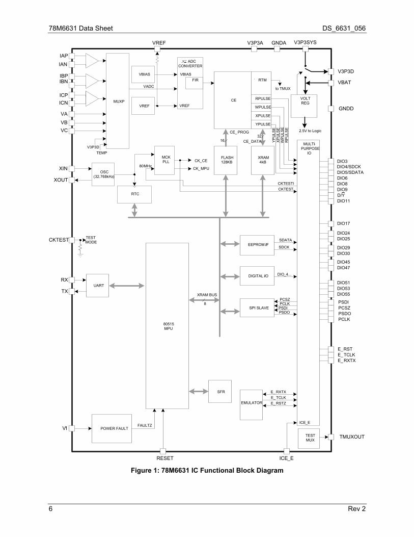
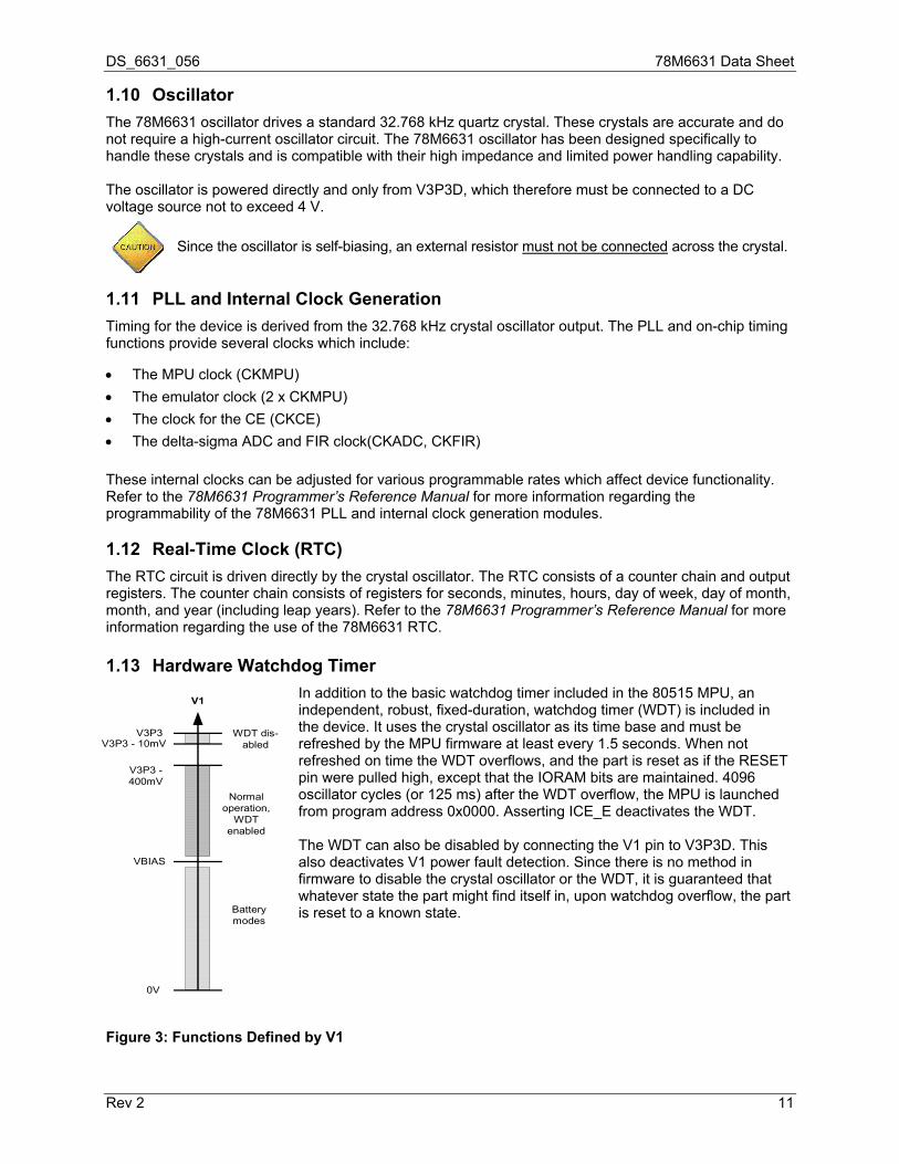
1.10 Oscillator The 78M6631 oscillator drives a standard 32.768 kHz quartz crystal. These crystals are accurate and do not require a high-current oscillator circuit. The 78M6631 oscillator has been designed specifically to handle these crystals and is compatible with their high impedance and limited power handling capability. The oscillator is powered directly and only from V3P3D, which therefore must be connected to a DC voltage source not to exceed 4 V.
V3P3
V3P3 -400mV
V3P3 - 10mV
VBIAS
0V
Batterymodes
Normaloperation,
WDTenabled
WDT dis-abled
V1
Since the oscillator is self-biasing, an external resistor must not be connected across the crystal.
1.11 PLL and Internal Clock Generation Timing for the device is derived from the 32.768 kHz crystal oscillator output. The PLL and on-chip timing functions provide several clocks which include:
The MPU clock (CKMPU)
The emulator clock (2 x CKMPU)
The clock for the CE (CKCE)
The delta-sigma ADC and FIR clock(CKADC, CKFIR)
These internal clocks can be adjusted for various programmable rates which affect device functionality. Refer to the 78M6631 Programmer’s Reference Manual for more information regarding the programmability of the 78M6631 PLL and internal clock generation modules. 1.12 Real-Time Clock (RTC) The RTC circuit is driven directly by the crystal oscillator. The RTC consists of a counter chain and output registers. The counter chain consists of registers for seconds, minutes, hours, day of week, day of month, month, and year (including leap years). Refer to the 78M6631 Programmer’s Reference Manual for more information regarding the use of the 78M6631 RTC.
1.13 Hardware Watchdog Timer In addition to the basic watchdog timer included in the 80515 MPU, an independent, robust, fixed-duration, watchdog timer (WDT) is included in the device. It uses the crystal oscillator as its time base and must be refreshed by the MPU firmware at least every 1.5 seconds. When not refreshed on time the WDT overflows, and the part is reset as if the RESET pin were pulled high, except that the IORAM bits are maintained. 4096 oscillator cycles (or 125 ms) after the WDT overflow, the MPU is launched from program address 0x0000. Asserting ICE_E deactivates the WDT. The WDT can also be disabled by connecting the V1 pin to V3P3D. This also deactivates V1 power fault detection. Since there is no method in firmware to disable the crystal oscillator or the WDT, it is guaranteed that whatever state the part might find itself in, upon watchdog overflow, the part is reset to a known state.
Figure 3: Functions Defined by V1
Rev 2 11
78M6631 Data Sheet DS_6631_056
1.14 Temperature Sensor The device includes an on-chip temperature sensor for determining the temperature of the bandgap reference. The primary use of the temperature data is to determine the magnitude of compensation required to offset the thermal drift in the system. 1.15 General-Purpose Digital I/O The 78M6631 includes 17 general-purpose digital I/O pins. As inputs, these pins are 5V compatible (no current-limiting resistors are needed). On reset or power-up, all DIO pins are inputs. Their input/output directions are subsequently set by the MPU. The digital I/O pins can be categorized as follows:
DIO3 (1 pin) DIO pin DIO4, DIO5 (2 pins) DIO/EEPROM DIO6 (1 pin) DIO pin (multifunction) DIO8, DIO9, DIO11 (3 pins) DIO pins DIO17 (1 pin) DIO pin DIO24, DIO25 (2 pins) DIO pins DIO29, DIO30 (2 pins) DIO pins DIO45, DIO47 (2 pins) DIO pins DIO51 (1 pin) DIO pin DIO53, DIO55 (2 pins) DIO pins
1.16 D/Y Selection Pin The D/Y pin selects either the Delta or the Wye configuration. At power-on, the Delta/Wye selection register assumes the state of the D/Y pin. The register value can be modified by the software overriding the state of the D/Y pin.
1.17 EEPROM Interface The 78M6631 provides hardware support for an optional 2-pin or a 3-wire (MICROWIRE®) EEPROM interface. 2-Pin EEPROM Interface The dedicated 2-pin serial interface communicates with external EEPROM devices. The interface is multiplexed onto the DIO4 (SDCK) and DIO5 (SDATA) pins.
3-Wire (MICROWIRE) EEPROM Interface A 500 kHz three-wire interface, using SDATA, SDCK and a DIO pin for CS, is also available.
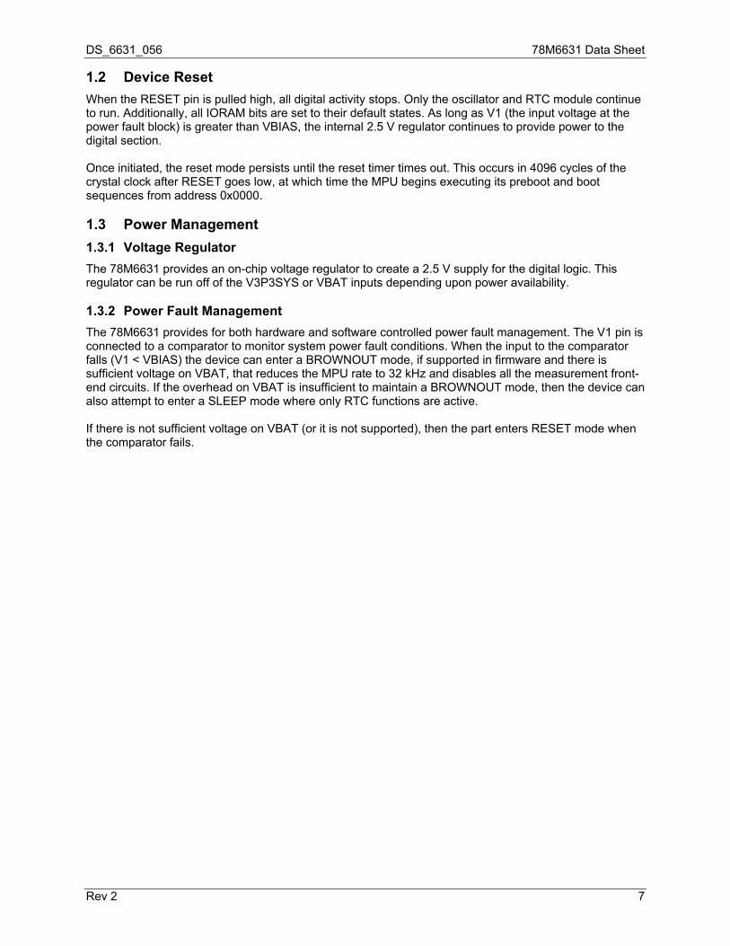
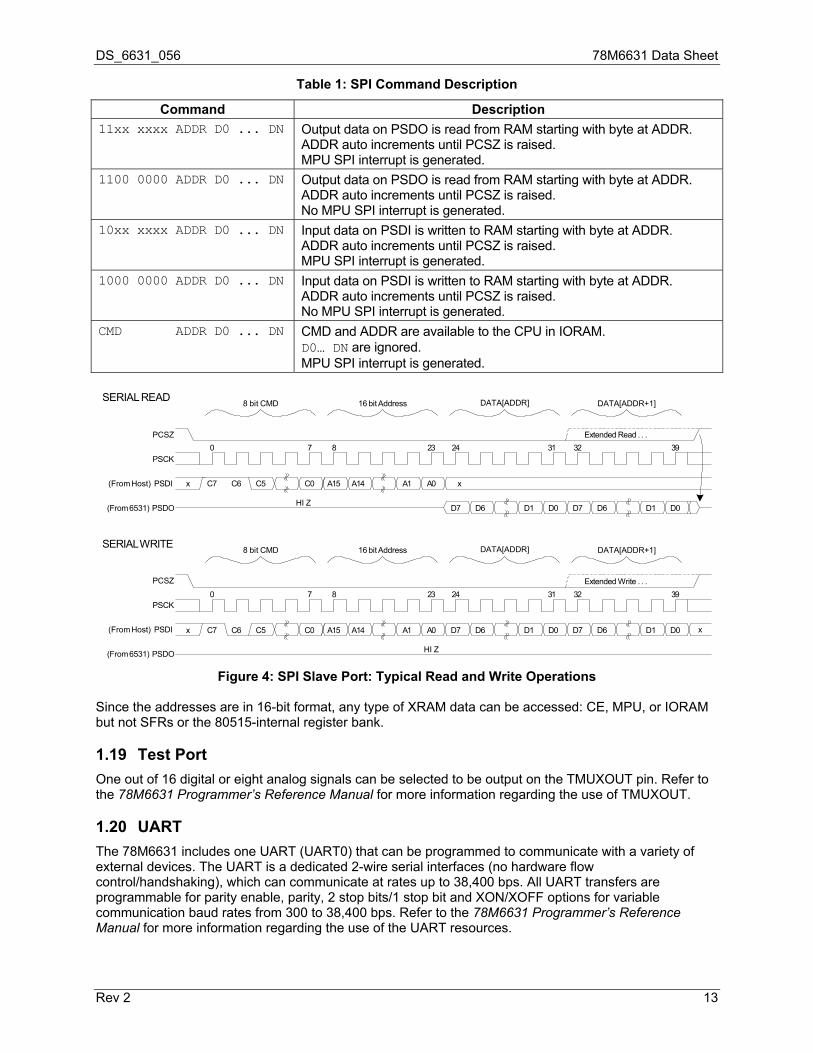
1.18 SPI Slave Port The slave SPI port communicates directly with the MPU data bus and is able to directly read and write XRAM and IORAM locations. It is also able to send commands to the MPU. The interface to the slave port consists of the PCSZ, PCLK, PSDI, and PSDO pins. A typical SPI transaction is as follows. While PCSZ is high, the port is held in an initialized/reset state. During this state, PSDO is held in high-Z state and all transitions on PCLK and PSDI are ignored. When PCSZ falls, the port begins the transaction on the first rising edge of PCLK. A transaction consists of an 8-bit command, a 16-bit address, and then one or more bytes of data. The transaction ends when PCSZ is raised. Some transactions can consist of a command only. The last SPI command and address (if part of the command) are available in the IORAM.
The SPI port supports data transfers at up to 1 Mbps. The SPI commands are described in Table 1 and Figure 4 illustrates the SPI Interface read and write timing. MICROWIRE is a registered trademark of National Semiconductor.
12 Rev 2
DS_6631_056 78M6631 Data Sheet
Table 1: SPI Command Description
Command Description 11xx xxxx ADDR D0 ... DN Output data on PSDO is read from RAM starting with byte at ADDR.
ADDR auto increments until PCSZ is raised. MPU SPI interrupt is generated.
1100 0000 ADDR D0 ... DN Output data on PSDO is read from RAM starting with byte at ADDR. ADDR auto increments until PCSZ is raised. No MPU SPI interrupt is generated.
10xx xxxx ADDR D0 ... DN Input data on PSDI is written to RAM starting with byte at ADDR. ADDR auto increments until PCSZ is raised. MPU SPI interrupt is generated.
1000 0000 ADDR D0 ... DN Input data on PSDI is written to RAM starting with byte at ADDR. ADDR auto increments until PCSZ is raised. No MPU SPI interrupt is generated.
CMD ADDR D0 ... DN CMD and ADDR are available to the CPU in IORAM. D0… DN are ignored. MPU SPI interrupt is generated.
A15 A14 A1 A0C0
0 31
x
D7 D6 D1 D0 D7 D6 D1 D0
C5C6C7x
PCSZ
PSCK
PSDI
PSDO
8 bit CMD 16 bit Address DATA[ADDR] DATA[ADDR+1]
7 8 23 24 32 39
Extended Read . . .
SERIAL READ
A15 A14 A1 A0C0
0 31
C5C6C7x
PCSZ
PSCK
PSDI
PSDO
8 bit CMD 16 bit Address DATA[ADDR] DATA[ADDR+1]
7 8 23 24 32 39
Extended Write . . .
SERIAL WRITE
D7 D6 D1 D0 D7 D6 D1 D0 x
HI Z
HI Z
(From Host)
(From 6531)
(From Host)
(From 6531) Figure 4: SPI Slave Port: Typical Read and Write Operations
Since the addresses are in 16-bit format, any type of XRAM data can be accessed: CE, MPU, or IORAM but not SFRs or the 80515-internal register bank. 1.19 Test Port One out of 16 digital or eight analog signals can be selected to be output on the TMUXOUT pin. Refer to the 78M6631 Programmer’s Reference Manual for more information regarding the use of TMUXOUT. 1.20 UART The 78M6631 includes one UART (UART0) that can be programmed to communicate with a variety of external devices. The UART is a dedicated 2-wire serial interfaces (no hardware flow control/handshaking), which can communicate at rates up to 38,400 bps. All UART transfers are programmable for parity enable, parity, 2 stop bits/1 stop bit and XON/XOFF options for variable communication baud rates from 300 to 38,400 bps. Refer to the 78M6631 Programmer’s Reference Manual for more information regarding the use of the UART resources.
Rev 2 13
78M6631 Data Sheet DS_6631_056
14 Rev 2
1.21 In-Circuit Emulator (ICE) Port The 78M6631 implements an In-Circuit Emulator (ICE) port for debug and programming of the device. To enable the use of the port the ICE_E pin must be pulled high. In this mode the E_RST, E_TCLK, and E_RXTX pins are enabled. Contact Maxim support for more information regarding the use of the ICE interface for device programming and debug.
DS_6631_056 78M6631 Data Sheet
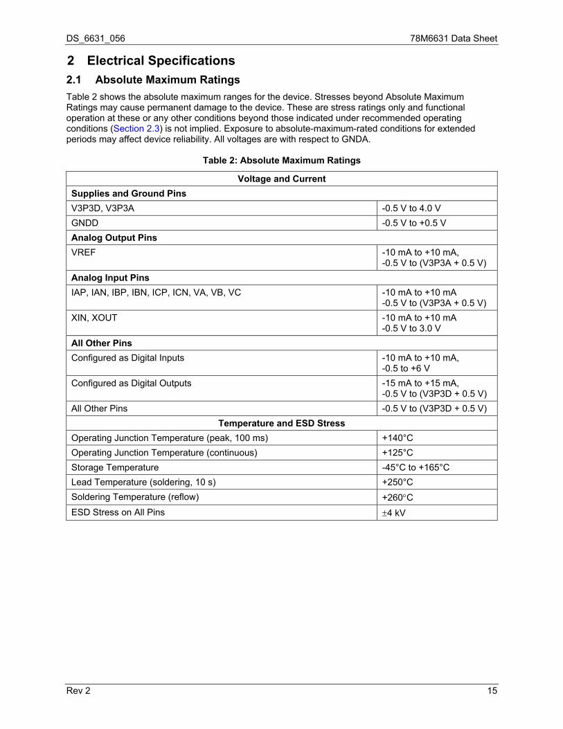
2 Electrical Specifications 2.1 Absolute Maximum Ratings Table 2 shows the absolute maximum ranges for the device. Stresses beyond Absolute Maximum Ratings may cause permanent damage to the device. These are stress ratings only and functional operation at these or any other conditions beyond those indicated under recommended operating conditions (Section 2.3) is not implied. Exposure to absolute-maximum-rated conditions for extended periods may affect device reliability. All voltages are with respect to GNDA.
Table 2: Absolute Maximum Ratings
Voltage and Current Supplies and Ground Pins V3P3D, V3P3A -0.5 V to 4.0 V
GNDD -0.5 V to +0.5 V
Analog Output Pins VREF -10 mA to +10 mA,
-0.5 V to (V3P3A + 0.5 V)
Analog Input Pins IAP, IAN, IBP, IBN, ICP, ICN, VA, VB, VC -10 mA to +10 mA
-0.5 V to (V3P3A + 0.5 V)
XIN, XOUT -10 mA to +10 mA -0.5 V to 3.0 V
All Other Pins Configured as Digital Inputs -10 mA to +10 mA,
-0.5 to +6 V
Configured as Digital Outputs -15 mA to +15 mA, -0.5 V to (V3P3D + 0.5 V)
All Other Pins -0.5 V to (V3P3D + 0.5 V)
Temperature and ESD Stress Operating Junction Temperature (peak, 100 ms) +140°C
Operating Junction Temperature (continuous) +125°C
Storage Temperature -45°C to +165°C
Lead Temperature (soldering, 10 s) +250°C
Soldering Temperature (reflow) +260C
ESD Stress on All Pins 4 kV
Rev 2 15
78M6631 Data Sheet DS_6631_056
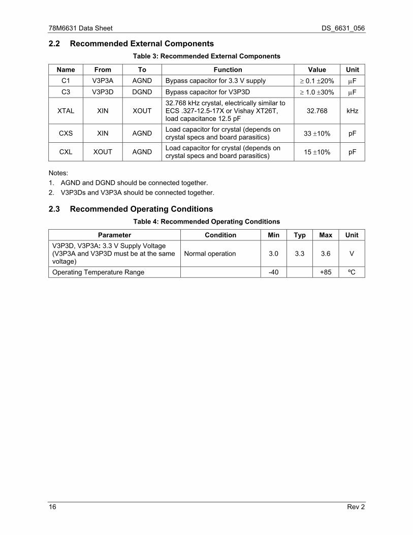
2.2 Recommended External Components Table 3: Recommended External Components
Name From To Function Value Unit C1 V3P3A AGND Bypass capacitor for 3.3 V supply 0.1 20% F
C3 V3P3D DGND Bypass capacitor for V3P3D 1.0 30% F
XTAL XIN XOUT 32.768 kHz crystal, electrically similar to ECS .327-12.5-17X or Vishay XT26T, load capacitance 12.5 pF
32.768 kHz
CXS XIN AGND Load capacitor for crystal (depends on crystal specs and board parasitics) 33 10% pF
CXL XOUT AGND Load capacitor for crystal (depends on crystal specs and board parasitics) 15 10% pF
Notes:
1. AGND and DGND should be connected together.
2. V3P3Ds and V3P3A should be connected together. 2.3 Recommended Operating Conditions
Table 4: Recommended Operating Conditions
Parameter Condition Min Typ Max Unit V3P3D, V3P3A: 3.3 V Supply Voltage (V3P3A and V3P3D must be at the same voltage)
Normal operation 3.0 3.3 3.6 V
Operating Temperature Range -40 +85 ºC
16 Rev 2
DS_6631_056 78M6631 Data Sheet
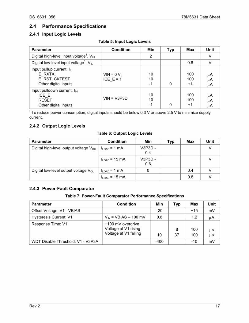
2.4 Performance Specifications 2.4.1 Input Logic Levels
Table 5: Input Logic Levels
Parameter Condition Min Typ Max Unit Digital high-level input voltage1, VIH 2 V
Digital low-level input voltage1, VIL 0.8 V
Input pullup current, IIL E_RXTX, E_RST, CKTEST Other digital inputs
VIN = 0 V, ICE_E = 1
10 10 -1
0
100 100 +1
A A A
Input pulldown current, IIH ICE_E RESET Other digital inputs
VIN = V3P3D
10 10 -1
0
100 100 +1
A A A
1 To reduce power consumption, digital inputs should be below 0.3 V or above 2.5 V to minimize supply current.
2.4.2 Output Logic Levels Table 6: Output Logic Levels
Parameter Condition Min Typ Max Unit ILOAD = 1 mA V3P3D -
0.4 V Digital high-level output voltage VOH
ILOAD = 15 mA V3P3D - 0.6
V
ILOAD = 1 mA 0 0.4 V Digital low-level output voltage VOL
ILOAD = 15 mA 0.8 V
2.4.3 Power-Fault Comparator
Table 7: Power-Fault Comparator Performance Specifications
Parameter Condition Min Typ Max Unit Offset Voltage: V1 - VBIAS -20 +15 mV
Hysteresis Current: V1 VIN = VBIAS – 100 mV 0.8 1.2 A
Response Time: V1 +100 mV overdrive Voltage at V1 rising Voltage at V1 falling
10
8
37
100 100
s s
WDT Disable Threshold: V1 - V3P3A -400 -10 mV
Rev 2 17
78M6631 Data Sheet DS_6631_056
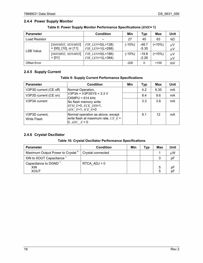
2.4.4 Power Supply Monitor Table 8: Power Supply Monitor Performance Specifications (BME= 1)
Parameter Condition Min Typ Max Unit Load Resistor – 27 45 63 kΩ
[M40MHZ, M26MHZ] = [00], [10], or [11]
FIR_LEN=0 (L=138) FIR_LEN=1 (L=288)
(-10%)
-48.7 -5.35
(+10%)
V V
LSB Value [M40MHZ, M26MHZ] = [01]
FIR_LEN=0 (L=186) FIR_LEN=1 (L=384)
(-10%)
-19.8 -2.26
(+10%)
V V
Offset Error -200 0 +100 mV
2.4.5 Supply Current
Table 9: Supply Current Performance Specifications
Parameter Condition Min Typ Max Unit V3P3D current (CE off) 4.2 6.35 mA
V3P3D current (CE on) 8.4 9.6 mA
V3P3A current
Normal Operation, V3P3A = V3P3SYS = 3.3 V CKMPU = 614 kHz No flash memory write RTM_E=0, ECK_DIS=1, ADC_E=1, ICE_E=0
3.3
3.8
mA
V3P3D current, Write Flash
Normal operation as above, except write flash at maximum rate, CE_E = 0, ADC_ E = 0
9.1 12 mA
2.4.6 Crystal Oscillator
Table 10: Crystal Oscillator Performance Specifications
Parameter Condition Min Typ Max Unit Maximum Output Power to Crystal 4 Crystal connected 1 W
XIN to XOUT Capacitance 1 3 pF
Capacitance to DGND 1 XIN XOUT
RTCA_ADJ = 0 5 5
pF pF
18 Rev 2
DS_6631_056 78M6631 Data Sheet
Rev 2 19
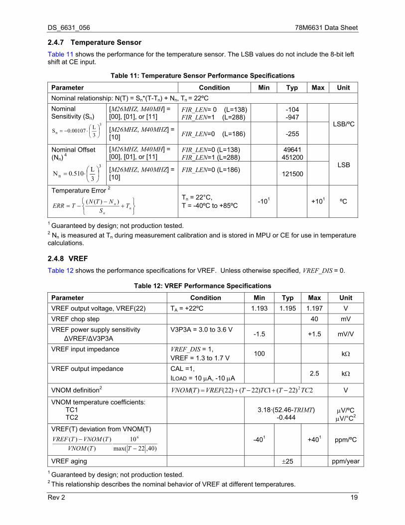
2.4.7 Temperature Sensor Table 11 shows the performance for the temperature sensor. The LSB values do not include the 8-bit left shift at CE input.
Table 11: Temperature Sensor Performance Specifications
Parameter Condition Min Typ Max Unit Nominal relationship: N(T) = Sn*(T-Tn) + Nn, Tn = 22ºC
[M26MHZ, M40MH] = [00], [01], or [11]
FIR_LEN= 0 (L=138) FIR_LEN=1 (L=288)
-104 -947
Nominal Sensitivity (Sn)
3
n 3L00107.0S
[M26MHZ, M40MHZ] =
[10] FIR_LEN=0 (L=186) -255 LSB/ºC
[M26MHZ, M40MH] = [00], [01], or [11]
FIR_LEN=0 (L=138) FIR_LEN=1 (L=288)
49641 451200
Nominal Offset (Nn)
4
3
n 3L510.0N
[M26MHZ, M40MHZ] = [10]
FIR_LEN=0 (L=186)
121500 LSB
Temperature Error 2
nn
n TS
NTNTERR
))(( Tn = 22°C, T = -40ºC to +85ºC
-101 +101 ºC
1 Guaranteed by design; not production tested. 2 Nn is measured at Tn during measurement calibration and is stored in MPU or CE for use in temperature calculations. 2.4.8 VREF Table 12 shows the performance specifications for VREF. Unless otherwise specified, VREF_DIS = 0.
Table 12: VREF Performance Specifications
Parameter Condition Min Typ Max Unit VREF output voltage, VREF(22) TA = +22ºC 1.193 1.195 1.197 V
VREF chop step 40 mV
VREF power supply sensitivity ΔVREF/ΔV3P3A
V3P3A = 3.0 to 3.6 V -1.5 +1.5 mV/V
VREF input impedance VREF_DIS = 1, VREF = 1.3 to 1.7 V
100 k
VREF output impedance CAL =1,
ILOAD = 10 A, -10 A 2.5 k
VNOM definition2 2)22(1)22()22()( 2TCTTCTVREFTVNOM V
VNOM temperature coefficients: TC1 TC2
3.18·(52.46-TRIMT)
-0.444
V/ºC V/°C2
VREF(T) deviation from VNOM(T)
)40,22max(10
)()()( 6
TTVNOMTVNOMTVREF
-401 +401 ppm/ºC
VREF aging 25 ppm/year
1 Guaranteed by design; not production tested. 2 This relationship describes the nominal behavior of VREF at different temperatures.
78M6631 Data Sheet DS_6631_056
20 Rev 2
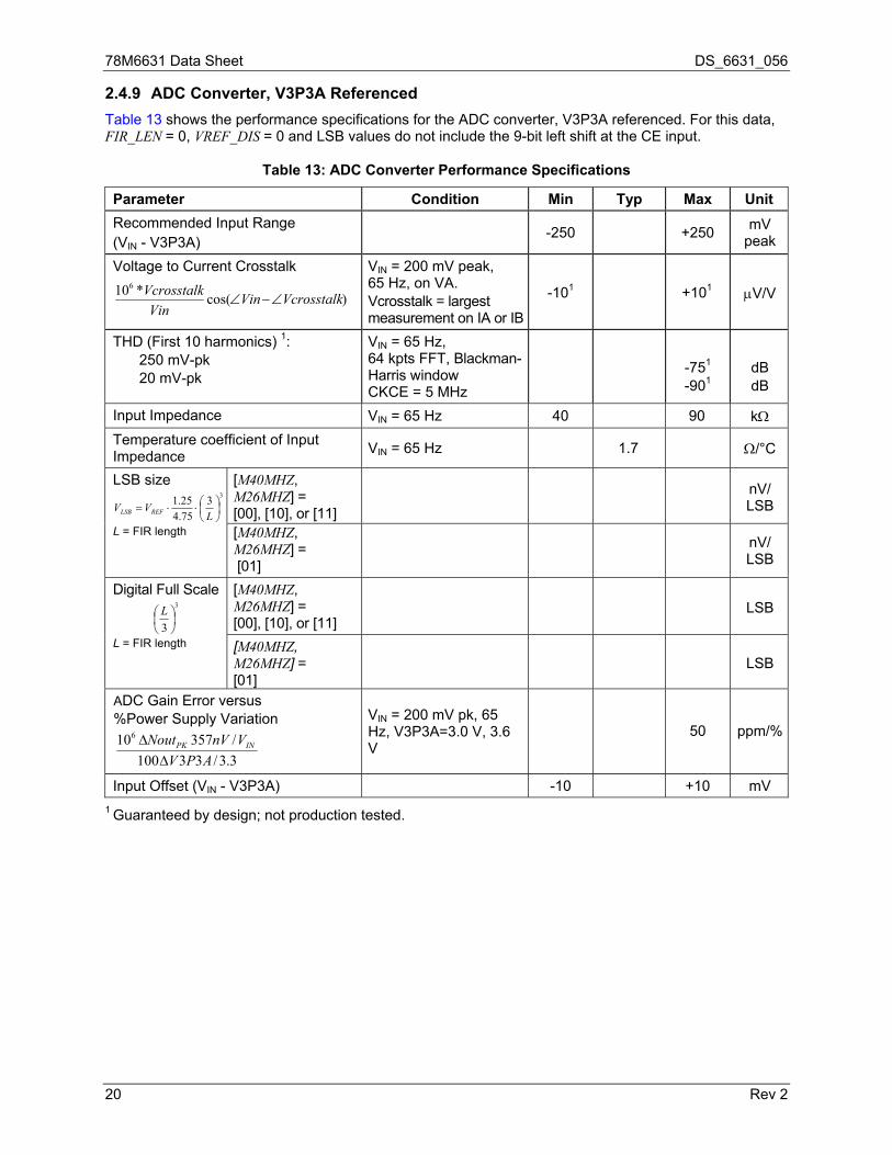
2.4.9 ADC Converter, V3P3A Referenced Table 13 shows the performance specifications for the ADC converter, V3P3A referenced. For this data, FIR_LEN = 0, VREF_DIS = 0 and LSB values do not include the 9-bit left shift at the CE input.
Table 13: ADC Converter Performance Specifications
Parameter Condition Min Typ Max Unit Recommended Input Range (VIN - V3P3A)
-250 +250 mV
peak
Voltage to Current Crosstalk
)cos(*106 VcrosstalkVinVin
Vcrosstalk
VIN = 200 mV peak, 65 Hz, on VA. Vcrosstalk = largest measurement on IA or IB
-101 +101 V/V
THD (First 10 harmonics) 1: 250 mV-pk 20 mV-pk
VIN = 65 Hz, 64 kpts FFT, Blackman-Harris window CKCE = 5 MHz
-751 -901
dB dB
Input Impedance VIN = 65 Hz 40 90 k
Temperature coefficient of Input Impedance
VIN = 65 Hz 1.7 /°C
[M40MHZ, M26MHZ] = [00], [10], or [11]
nV/ LSB
LSB size 33
75.425.1
LVV REFLSB
L = FIR length [M40MHZ, M26MHZ] = [01]
nV/ LSB
[M40MHZ, M26MHZ] = [00], [10], or [11]
LSB Digital Full Scale
3
3
L
L = FIR length [M40MHZ, M26MHZ] = [01]
LSB
ADC Gain Error versus %Power Supply Variation
3.3/33100/357106
APVVnVNout INPK
VIN = 200 mV pk, 65 Hz, V3P3A=3.0 V, 3.6 V
50 ppm/%
Input Offset (VIN - V3P3A) -10 +10 mV
1 Guaranteed by design; not production tested.
DS_6631_056 78M6631 Data Sheet
2.5 Timing Specifications 2.5.1 Flash Memory
Table 14: Flash Memory Timing Specifications
Parameter Condition Min Typ Max Unit Flash write cycles -40°C to +85°C 20,000 Cycles
Flash data retention +25°C 100 Years
Flash data retention +85°C 10 Years
Flash byte write operations between page or mass erase operations
2 Cycles
Write Time per Byte 42 s
Page Erase (1024 bytes) 20 ms
Mass Erase 200 ms
2.5.2 EEPROM Interface
Table 15: EEPROM Interface Timing
Parameter Condition Min Typ Max Unit CKMPU = 4.9152 MHz, using interrupts
78 kHz Write Clock frequency (I2C)
CKMPU = 4.9152 MHz, bit-banging DIO4/5
150 kHz
Write Clock frequency (3-wire) CKMPU = 4.9152 MHz 500 kHz
2.5.3 RESET
Table 16: RESET Timing
Parameter Condition Min Typ Max Unit Reset pulse width 5 s
Reset pulse fall time 11 s
1 Guaranteed by design; not production tested.
Rev 2 21
78M6631 Data Sheet DS_6631_056
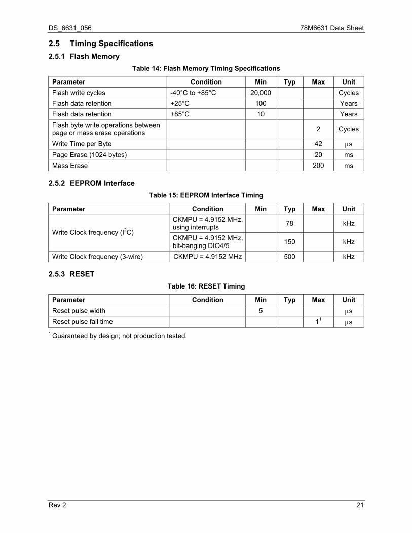
2.5.4 SPI Slave Port Table 17: SPI Slave Port Timing
Parameter Condition Min Typ Max Unit tSPIcyc PCLK cycle time 1 s
tSPILead Enable lead time 15 ns
tSPILag Enable lag time 0 ns
High
40 tSPIW PCLK pulse width
Low 40 ns
tSPISCK PCSZ to first PCLK fall Ignore if PCLK is low when PCSZ falls
2 ns
tSPIDIS Disable time 0 ns
tSPIEV PCLK to Data Out 15 ns
tSPISU Data input setup time 10 ns
tSPIH Data input hold time 5 ns
MSB OUT LSB OUT
MSB IN LSB IN
tSPIcyctSPILead tSPILag
tSPISCK
tSPIH
tSPIW tSPIEV tSPIW tSPIDIS
PCSZ
PCLK
PSDI
PSDO
Figure 5: SPI Slave Port Timing
22 Rev 2
DS_6631_056 78M6631 Data Sheet
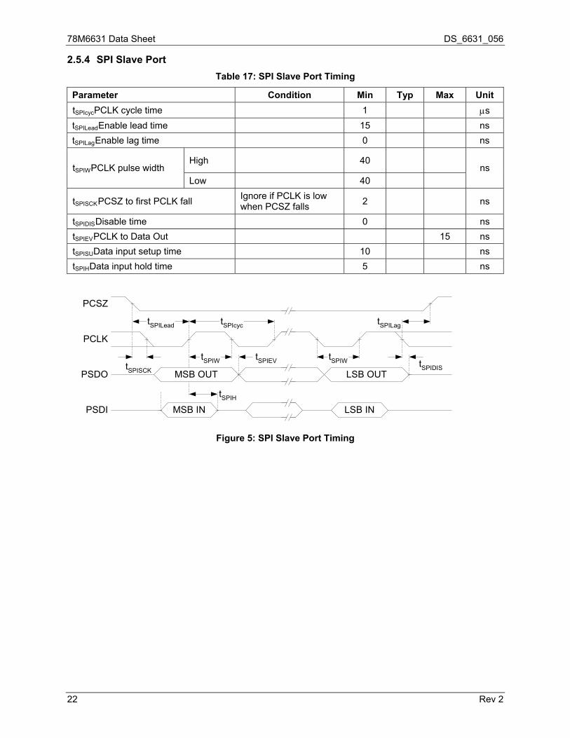
3 Packaging 3.1 56-Pin QFN Package 3.2 Pinout
Figure 6: Pinout for QFN-56 Package
Rev 2 23
78M6631 Data Sheet DS_6631_056
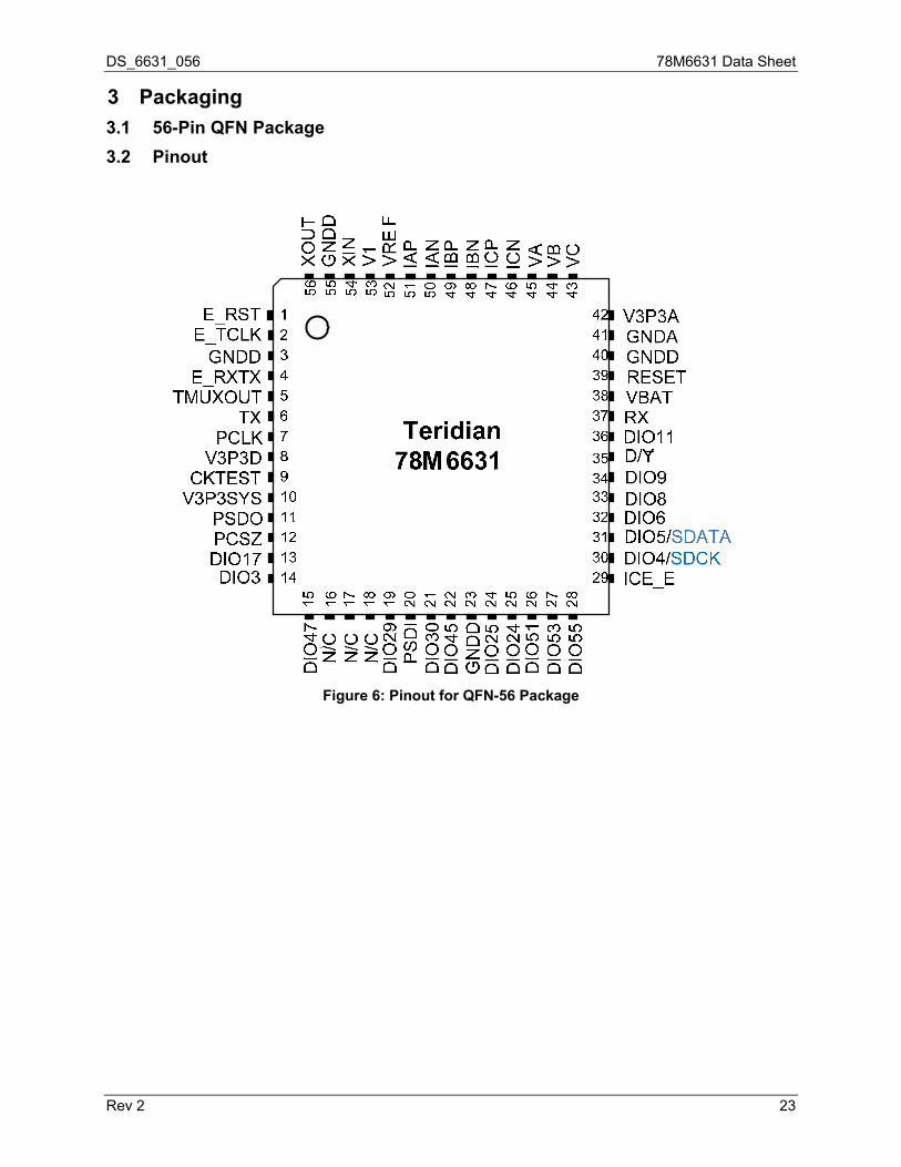
3.2.1 56-Pin QFN Package Outline
24 Rev 2
DS_6631_056 78M6631 Data Sheet
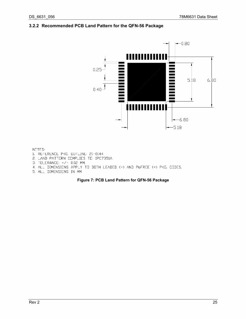
3.2.2 Recommended PCB Land Pattern for the QFN-56 Package
Figure 7: PCB Land Pattern for QFN-56 Package
Rev 2 25
78M6631 Data Sheet DS_6631_056
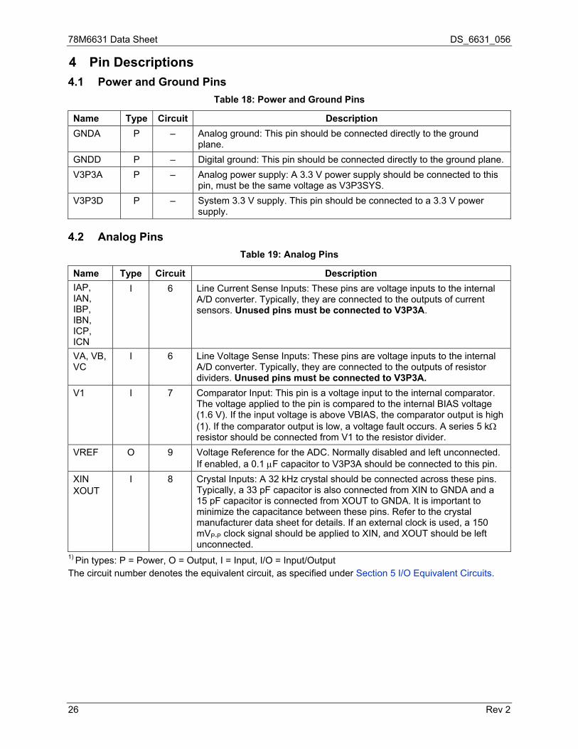
4 Pin Descriptions 4.1 Power and Ground Pins
Table 18: Power and Ground Pins
Name Type Circuit Description GNDA P – Analog ground: This pin should be connected directly to the ground
plane.
GNDD P – Digital ground: This pin should be connected directly to the ground plane.
V3P3A P – Analog power supply: A 3.3 V power supply should be connected to this pin, must be the same voltage as V3P3SYS.
V3P3D P – System 3.3 V supply. This pin should be connected to a 3.3 V power supply.
4.2 Analog Pins
Table 19: Analog Pins
Name Type Circuit Description IAP, IAN, IBP, IBN, ICP, ICN
I 6 Line Current Sense Inputs: These pins are voltage inputs to the internal A/D converter. Typically, they are connected to the outputs of current sensors. Unused pins must be connected to V3P3A.
VA, VB, VC
I 6 Line Voltage Sense Inputs: These pins are voltage inputs to the internal A/D converter. Typically, they are connected to the outputs of resistor dividers. Unused pins must be connected to V3P3A.
V1 I 7 Comparator Input: This pin is a voltage input to the internal comparator. The voltage applied to the pin is compared to the internal BIAS voltage (1.6 V). If the input voltage is above VBIAS, the comparator output is high (1). If the comparator output is low, a voltage fault occurs. A series 5 k resistor should be connected from V1 to the resistor divider.
VREF O 9 Voltage Reference for the ADC. Normally disabled and left unconnected. If enabled, a 0.1 F capacitor to V3P3A should be connected to this pin.
XIN XOUT
I 8 Crystal Inputs: A 32 kHz crystal should be connected across these pins. Typically, a 33 pF capacitor is also connected from XIN to GNDA and a 15 pF capacitor is connected from XOUT to GNDA. It is important to minimize the capacitance between these pins. Refer to the crystal manufacturer data sheet for details. If an external clock is used, a 150 mVP-P clock signal should be applied to XIN, and XOUT should be left unconnected.
1) Pin types: P = Power, O = Output, I = Input, I/O = Input/Output The circuit number denotes the equivalent circuit, as specified under Section 5 I/O Equivalent Circuits.
26 Rev 2
DS_6631_056 78M6631 Data Sheet
Rev 2 27
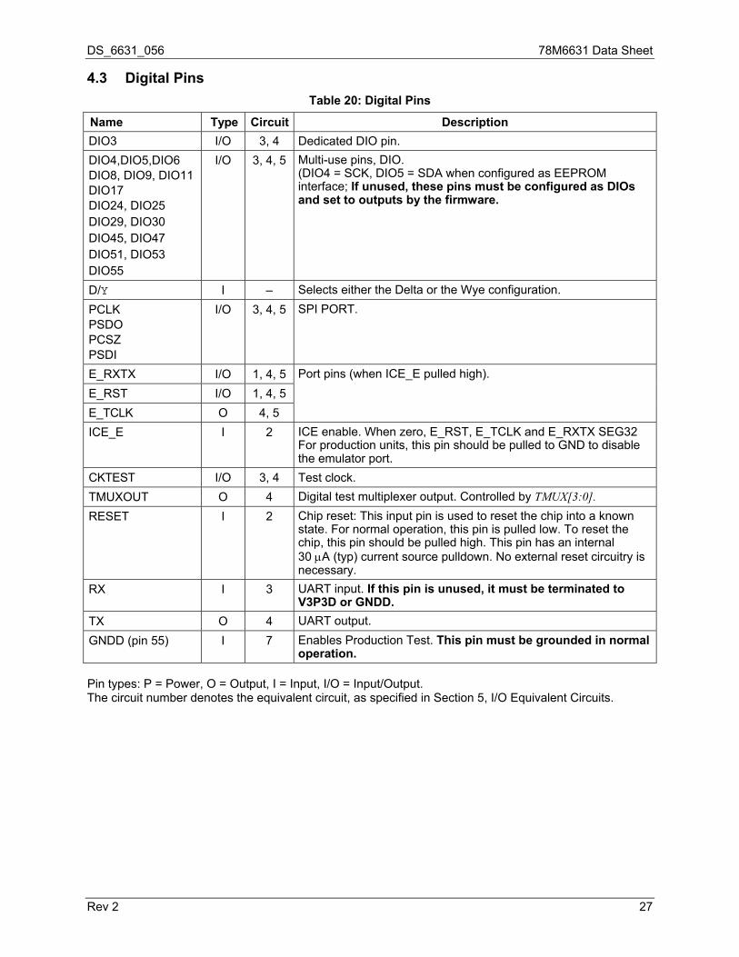
4.3 Digital Pins Table 20: Digital Pins
Name Type Circuit Description DIO3 I/O 3, 4 Dedicated DIO pin.
DIO4,DIO5,DIO6 DIO8, DIO9, DIO11 DIO17 DIO24, DIO25 DIO29, DIO30 DIO45, DIO47 DIO51, DIO53 DIO55
I/O 3, 4, 5 Multi-use pins, DIO. (DIO4 = SCK, DIO5 = SDA when configured as EEPROM interface; If unused, these pins must be configured as DIOs and set to outputs by the firmware.
D/Y I – Selects either the Delta or the Wye configuration.
PCLK PSDO PCSZ PSDI
I/O 3, 4, 5 SPI PORT.
E_RXTX I/O 1, 4, 5
E_RST I/O 1, 4, 5
E_TCLK O 4, 5
Port pins (when ICE_E pulled high).
ICE_E I 2 ICE enable. When zero, E_RST, E_TCLK and E_RXTX SEG32 For production units, this pin should be pulled to GND to disable the emulator port.
CKTEST I/O 3, 4 Test clock.
TMUXOUT O 4 Digital test multiplexer output. Controlled by TMUX[3:0]. RESET I 2 Chip reset: This input pin is used to reset the chip into a known
state. For normal operation, this pin is pulled low. To reset the chip, this pin should be pulled high. This pin has an internal 30 A (typ) current source pulldown. No external reset circuitry is necessary.
RX I 3 UART input. If this pin is unused, it must be terminated to V3P3D or GNDD.
TX O 4 UART output.
GNDD (pin 55) I 7 Enables Production Test. This pin must be grounded in normal operation.
Pin types: P = Power, O = Output, I = Input, I/O = Input/Output. The circuit number denotes the equivalent circuit, as specified in Section 5, I/O Equivalent Circuits.
78M6631 Data Sheet DS_6631_056
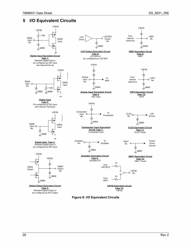
5 I/O Equivalent Circuits
Oscillator Equivalent CircuitType 8:
Oscillator I/O
Digital Input Equivalent CircuitType 1:
Standard Digital Input orpin configured as DIO Input
with Internal Pull-Up
GNDD
110K
V3P3D
CMOSInput
V3P3D
DigitalInputPin
Digital InputType 2:
Pin configured as DIO Inputwith Internal Pull-Down
GNDD
110K
GNDD
CMOSInput
V3P3D
DigitalInputPin
Digital Input Type 3:Standard Digital Input or
pin configured as DIO Input
GNDD
CMOSInput
V3P3D
DigitalInputPin
CMOSOutput
GNDD
V3P3D
GNDD
V3P3D
Digital Output Equivalent CircuitType 4:
Standard Digital Output orpin configured as DIO Output
DigitalOutput
Pin
LCD Output Equivalent CircuitType 5:
LCD SEG orpin configured as LCD SEG
LCDDriver
GNDD
LCD SEGOutput
Pin
ToMUX
GNDA
V3P3A
Analog Input Equivalent CircuitType 6:
ADC Input
AnalogInputPin
Comparator Input EquivalentCircuit Type 7:Comparator Input
GNDA
V3P3A
ToComparator
ComparatorInputPin
ToOscillator
GNDD
OscillatorPin
VREF Equivalent CircuitType 9:
VREF
frominternal
reference
GNDA
V3P3A
VREFPin
V2P5 Equivalent CircuitType 10:
V2P5
frominternal
reference
GNDD
V3P3D
V2P5Pin
VLCD Equivalent CircuitType 11:
VLCD Power
GNDD
LCDDrivers
VLCDPin
VBAT Equivalent CircuitType 12:
VBAT Power
GNDD
PowerDown
Circuits
VBATPin
V3P3D Equivalent CircuitType 13:V3P3D
fromV3P3SYS
V3P3DPin
fromVBAT
10
40
Figure 8: I/O Equivalent Circuits
28 Rev 2
DS_6631_056 78M6631 Data Sheet
Rev 2 29
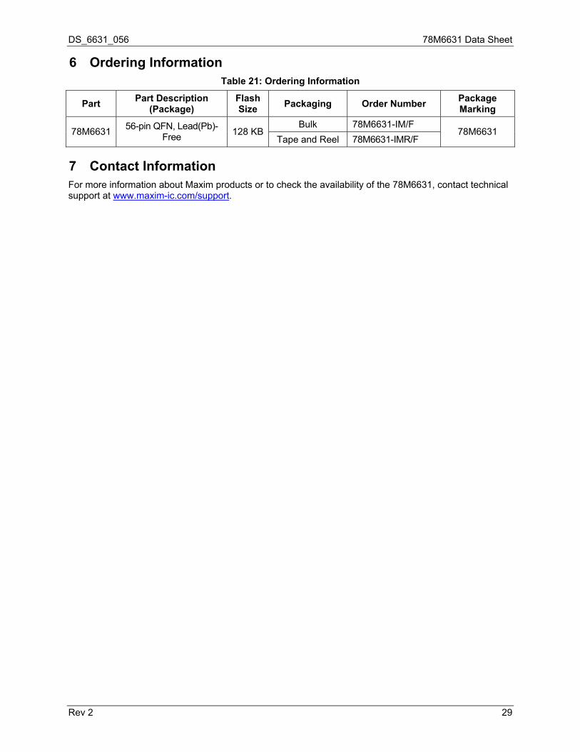
6 Ordering Information Table 21: Ordering Information
Part Part Description (Package)
Flash Size Packaging Order Number Package
Marking Bulk 78M6631-IM/F
78M6631 56-pin QFN, Lead(Pb)-
Free 128 KB
Tape and Reel 78M6631-IMR/F 78M6631
7 Contact Information For more information about Maxim products or to check the availability of the 78M6631, contact technical support at www.maxim-ic.com/support.
DS_6631_056 78M6631 Data Sheet
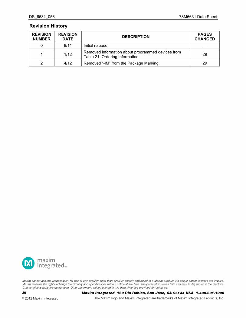
Revision History REVISION NUMBER
REVISION DATE DESCRIPTION PAGES
CHANGED 0 9/11 Initial release
1 1/12 Removed information about programmed devices from Table 21. Ordering Information
29
2 4/12 Removed “-IM” from the Package Marking 29
30 Maxim Integrated 160 Rio Robles, San Jose, CA 95134 USA 1-408-601-1000
Maxim cannot assume responsibility for use of any circuitry other than circuitry entirely embodied in a Maxim product. No circuit patent licenses are implied. Maxim reserves the right to change the circuitry and specifications without notice at any time. The parametric values (min and max limits) shown in the Electrical Characteristics table are guaranteed. Other parametric values quoted in this data sheet are provided for guidance.
© 2012 Maxim Integrated The Maxim logo and Maxim Integrated are trademarks of Maxim Integrated Products, Inc.