Embed Size (px)
Citation preview
- 1 -
Rev. 1.5, Apr. 2015
SAMSUNG ELECTRONICS RESERVES THE RIGHT TO CHANGE PRODUCTS, INFORMATION AND SPECIFICATIONS WITHOUT NOTICE.
Products and specifications discussed herein are for reference purposes only. All information discussed herein is provided on an "AS IS" basis, without warranties of any kind.
This document and all information discussed herein remain the sole and exclusive property of Samsung Electronics. No license of any patent, copyright, mask work, trademark or any other intellectual property right is granted by one party to the other party under this document, by implication, estoppel or other-wise.
Samsung products are not intended for use in life support, critical care, medical, safety equipment, or similar applications where product failure could result in loss of life or personal or physical harm, or any military or defense application, or any governmental procurement to which special terms or provisions may apply.
For updates or additional information about Samsung products, contact your nearest Samsung office.
All brand names, trademarks and registered trademarks belong to their respective owners.
2015 Samsung Electronics Co., Ltd. All rights reserved.
datasheet
M393B1G70EB0M393B1G73EB0M393B2G70EB0
240pin Registered DIMM based on 4Gb E-die 78FBGA with Lead-Free & Halogen-Free(RoHS compliant)
1.35V

- 2 -
datasheet DDR3L SDRAMRev. 1.5
Registered DIMM
Revision History
Revision No. History Draft Date Remark Editor
1.0 - First SPEC. Release Aug. 2013 - S.H.Kim
1.01 - Separate Mono and DDP datasheet Dec. 2013 - S.H.Kim
(This datasheet is only Mono device.)
1.1 - Addition of 8GB(1Rx4, 2Rx8) RDIMM Mar. 2014 - S.H.Kim
1.2 - Deletion of 8GB(1Rx4, 2Rx8) RDIMM May. 2014 - S.H.Kim
1.3 - Change of Physical Dimensions on page 36 Oct. 2014 - J.Y.Lee
1.4 - Change of Part Number Dec. 2014 - J.Y.Lee
- Change Physical Dimensions on page 36
1.5 - Addition of 8GB(1Rx4, 2Rx8) RDIMM Apr. 2015 - J.Y.Lee
- 3 -
datasheet DDR3L SDRAMRev. 1.5
Registered DIMM
Table Of Contents
240pin Registered DIMM based on 4Gb E-die1. DDR3L Registered DIMM Ordering Information ...........................................................................................................4
2. Key Features.................................................................................................................................................................4
3. Address Configuration ..................................................................................................................................................4
4. Registered DIMM Pin Configurations (Front side/Back side)........................................................................................5
5. Pin Description .............................................................................................................................................................6
6. ON DIMM Thermal Sensor ...........................................................................................................................................6
7. Input/Output Functional Description..............................................................................................................................7
8. Pinout Comparison Based On Module Type.................................................................................................................8
9. Registering Clock Driver Specification..........................................................................................................................99.1 Timing & Capacitance values .................................................................................................................................. 99.2 Clock driver Characteristics..................................................................................................................................... 9
10. Function Block Diagram:.............................................................................................................................................1010.1 8GB, 1Gx72 Module (Populated as 1 rank of x4 DDR3 SDRAMs) .......................................................................1010.2 8GB, 1Gx72 Module (Populated as 2 ranks of x8 DDR3 SDRAMs)......................................................................1110.3 16GB, 2Gx72 Module (Populated as 2 ranks of x4 DDR3 SDRAMs)....................................................................12
11. Absolute Maximum Ratings ........................................................................................................................................1411.1 Absolute Maximum DC Ratings............................................................................................................................. 1411.2 DRAM Component Operating Temperature Range ..............................................................................................14
12. AC & DC Operating Conditions...................................................................................................................................1412.1 Recommended DC Operating Conditions .............................................................................................................14
13. AC & DC Input Measurement Levels ..........................................................................................................................1513.1 AC & DC Logic Input Levels for Single-ended Signals..........................................................................................1513.2 VREF Tolerances .................................................................................................................................................. 1713.3 AC and DC Logic Input Levels for Differential Signals ..........................................................................................18
13.3.1. Differential Signals Definition ......................................................................................................................... 1813.3.2. Differential Swing Requirement for Clock (CK - CK) and Strobe (DQS - DQS) .............................................1813.3.3. Single-ended Requirements for Differential Signals ......................................................................................1913.3.4. Differential Input Cross Point Voltage ............................................................................................................20
13.4 Slew Rate Definition for Single Ended Input Signals.............................................................................................2213.5 Slew Rate Definition for Differential Input Signals .................................................................................................22
14. AC & DC Output Measurement Levels .......................................................................................................................2214.1 Single Ended AC and DC Output Levels...............................................................................................................2214.2 Differential AC and DC Output Levels ...................................................................................................................2214.3 Single-ended Output Slew Rate ............................................................................................................................ 2314.4 Differential Output Slew Rate ................................................................................................................................ 24
15. IDD specification definition..........................................................................................................................................25
16. IDD SPEC Table .........................................................................................................................................................27
17. Input/Output Capacitance ...........................................................................................................................................29
18. Electrical Characteristics and AC timing .....................................................................................................................3018.1 Refresh Parameters by Device Density.................................................................................................................3018.2 Speed Bins and CL, tRCD, tRP, tRC and tRAS for Corresponding Bin ................................................................3018.3 Speed Bins and CL, tRCD, tRP, tRC and tRAS for Corresponding Bin ................................................................30
18.3.1. Speed Bin Table Notes .................................................................................................................................. 33
19. Timing Parameters by Speed Grade ..........................................................................................................................3419.1 Jitter Notes ............................................................................................................................................................ 3719.2 Timing Parameter Notes........................................................................................................................................ 38
20. Physical Dimensions...................................................................................................................................................3920.1 1Gbx4 based 1Gx72 Module (1 Rank) - M393B1G70EB0....................................................................................39
20.1.1. x72 DIMM, populated as one physical rank of x4 DDR3 SDRAMs................................................................3920.2 512Mbx8 based 1Gx72 Module (2 Ranks) - M393B1G73EB0..............................................................................40
20.2.1. x72 DIMM, populated as two physical ranks of x8 DDR3 SDRAMs...............................................................4020.3 1Gbx4 based 2Gx72 Module (2 Ranks) - M393B2G70EB0 ..................................................................................41
20.3.1. x72 DIMM, populated as two physical ranks of x4 DDR3 SDRAMs...............................................................41

- 4 -
datasheet DDR3L SDRAMRev. 1.5
Registered DIMM
1. DDR3L Registered DIMM Ordering Information
NOTE :1. K0(1600Mbps 11-11-11) - DDR3L-1600(11-11-11) is backward compatible to DDR3L-1333(9-9-9)
2. Key Features
• JEDEC standard 1.35V(1.28V~1.45V) & 1.5V(1.425V~1.575V) Power Supply• VDDQ = 1.35V(1.28V~1.45V) & 1.5V(1.425V~1.575V)• 400MHz fCK for 800Mb/sec/pin, 533MHz fCK for 1066Mb/sec/pin, 667MHz fCK for 1333Mb/sec/pin, 800MHz fCK for 1600Mb/sec/pin• 8 independent internal bank• Programmable CAS Latency: 6,7,8,9,10,11• Programmable Additive Latency(Posted CAS) : 0, CL - 2, or CL - 1 clock• Programmable CAS Write Latency(CWL) = 5(DDR3-800), 6(DDR3-1066), 7(DDR3-1333) and 8(DDR3-1600)• 8-bit pre-fetch• Burst Length: 8 (Interleave without any limit, sequential with starting address “000” only), 4 with tCCD = 4 which does not allow seamless read or
write [either On the fly using A12 or MRS]• Bi-directional Differential Data Strobe• Internal(self) calibration : Internal self calibration through ZQ pin (RZQ : 240 ohm ± 1%)• On Die Termination using ODT pin• Average Refresh Period 7.8us at lower then TCASE 85C, 3.9us at 85C < TCASE 95C• Asynchronous Reset
3. Address Configuration
Part Number1 Density Organization Component Composition Number of Rank Height
M393B1G70EB0-YK0 8GB 1Gx72 1Gx4(K4B4G0446E-BYK0)*18 1 30mm
M393B1G73EB0-YK0 8GB 1Gx72 512Mx8(K4B4G0846E-BYK0)*18 2 30mm
M393B2G70EB0-YK0 16GB 2Gx72 1Gx4(K4B4G0446E-BYK0)*36 2 30mm
SpeedDDR3-800 DDR3-1066 DDR3-1333 DDR3-1600
Unit6-6-6 7-7-7 9-9-9 11-11-11
tCK(min) 2.5 1.875 1.5 1.25 ns
CAS Latency 6 7 9 11 nCK
tRCD(min) 15 13.125 13.5 13.75 ns
tRP(min) 15 13.125 13.5 13.75 ns
tRAS(min) 37.5 37.5 36 35 ns
tRC(min) 52.5 50.625 49.5 48.75 ns
Organization Row Address Column Address Bank Address Auto Precharge
512Mx8(4Gb) based Module A0-A15 A0-A9 BA0-BA2 A10/AP
1Gx4(4Gb) based Module A0-A15 A0-A9, A11 BA0-BA2 A10/AP

- 5 -
datasheet DDR3L SDRAMRev. 1.5
Registered DIMM
4. Registered DIMM Pin Configurations (Front side/Back side)
NOTE : NC = No internal ConnectionSAMSUNG ELECTRONICS CO., Ltd. reserves the right to change products and specifications without notice.
Pin Front Pin Back Pin Front Pin Back Pin Front Pin Back1 VREFDQ 121 VSS 42 DQS8 162 NC,DQS17
,TDQS17 82 DQ33 202 VSS
2 VSS 122 DQ4 43 DQS8 163 VSS 83 VSS 203 DM4,DQS13,TDQS13
3 DQ0 123 DQ5 44 VSS 164 CB6,NC 84 DQS4 204 NC,DQS13,TDQS13
4 DQ1 124 VSS 45 CB2,NC 165 CB7,NC 85 DQS4 205 VSS
5 VSS 125 DM0,DQS9,TDQS9 46 CB3,NC 166 VSS 86 VSS 206 DQ38
6 DQS0 126 NC,DQS9,TDQS9 47 VSS 167 NC(TEST) 87 DQ34 207 DQ39
7 DQS0 127 VSS 48 VTT, NC 168 RESET 88 DQ35 208 VSS
8 VSS 128 DQ6 KEY 89 VSS 209 DQ44
9 DQ2 129 DQ7 49 VTT, NC 169 CKE1, NC 90 DQ40 210 DQ45
10 DQ3 130 VSS 50 CKE0 170 VDD 91 DQ41 211 VSS
11 VSS 131 DQ12 51 VDD 171 A15 92 VSS 212 DM5,DQS14,TDQS14
12 DQ8 132 DQ13 52 BA2 172 A14 93 DQS5 213 NC,DQS14,TDQS14
13 DQ9 133 VSS 53 Err_Out/NC 173 VDD 94 DQS5 214 VSS
14 VSS 134 DM1,DQS10,TDQS10 54 VDD 174 A12/BC 95 VSS 215 DQ46
15 DQS1 135 NC,DQS10,TDQS10 55 A11 175 A9 96 DQ42 216 DQ47
16 DQS1 136 VSS 56 A7 176 VDD 97 DQ43 217 VSS
17 VSS 137 DQ14 57 VDD 177 A8 98 VSS 218 DQ52
18 DQ10 138 DQ15 58 A5 178 A6 99 DQ48 219 DQ53
19 DQ11 139 VSS 59 A4 179 VDD 100 DQ49 220 VSS
20 VSS 140 DQ20 60 VDD 180 A3 101 VSS 221 DM6,DQS15,TDQS15
21 DQ16 141 DQ21 61 A2 181 A1 102 DQS6 222 NC,DQS15,TDQS15
22 DQ17 142 VSS 62 VDD 182 VDD 103 DQS6 223 VSS
23 VSS 143 DM2,DQS11,TDQS11 63 NC, CK1 183 VDD 104 VSS 224 DQ54
24 DQS2 144 NC,DQS11,TDQS11 64 NC, CK1 184 CK0 105 DQ50 225 DQ55
25 DQS2 145 VSS 65 VDD 185 CK0 106 DQ51 226 VSS
26 VSS 146 DQ22 66 VDD 186 VDD 107 VSS 227 DQ60
27 DQ18 147 DQ23 67 VREFCA 187 EVENT,NC 108 DQ56 228 DQ61
28 DQ19 148 VSS 68 NC/Par_In 188 A0 109 DQ57 229 VSS
29 VSS 149 DQ28 69 VDD 189 VDD 110 VSS 230 DM7/DQS16TDQS16
30 DQ24 150 DQ29 70 A10/AP 190 BA1 111 DQS7 231 DM7,DQS16,TDQS16
31 DQ25 151 VSS 71 BA0 191 VDD 112 DQS7 232 VSS
32 VSS 152 DM3,DQS12,TDQS12 72 VDD 192 RAS 113 VSS 233 DQ62
33 DQS3 153 NC,DQS12,TDQS12 73 WE 193 S0 114 DQ58 234 DQ63
34 DQS3 154 VSS 74 CAS 194 VDD 115 DQ59 235 VSS
35 VSS 155 DQ30 75 VDD 195 ODT0 116 VSS 236 VDDSPD
36 DQ26 156 DQ31 76 S1,NC 196 A13 117 SA0 237 SA1
37 DQ27 157 VSS 77 ODT1,NC 197 VDD 118 SCL 238 SDA
38 VSS 158 CB4,NC 78 VDD 198 S3,NC 119 SA2 239 VSS
39 CB0,NC 159 CB5,NC 79 S2,NC 199 VSS 120 VTT 240 VTT
40 CB1,NC 160 VSS 80 VSS 200 DQ36
41 VSS 161 DM8,DQS17TDQS17,NC 81 DQ32 201 DQ37
- 6 -
datasheet DDR3L SDRAMRev. 1.5
Registered DIMM
5. Pin Description
NOTE : *The VDD and VDDQ pins are tied common to a single power-plane on these designs.
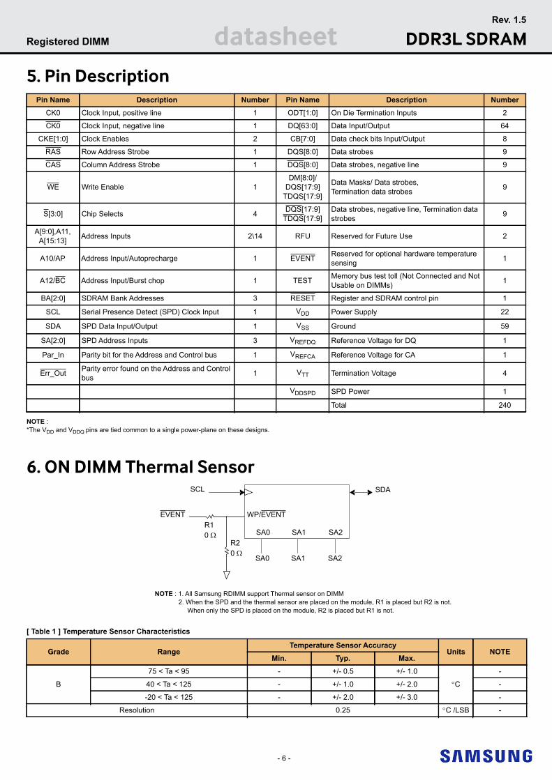
6. ON DIMM Thermal SensorSCL SDA
WP/EVENT
SA0 SA1 SA2
SA0 SA1 SA2
EVENTR10
R20
NOTE : 1. All Samsung RDIMM support Thermal sensor on DIMM 2. When the SPD and the thermal sensor are placed on the module, R1 is placed but R2 is not.
When only the SPD is placed on the module, R2 is placed but R1 is not.
[ Table 1 ] Temperature Sensor Characteristics
Pin Name Description Number Pin Name Description Number
CK0 Clock Input, positive line 1 ODT[1:0] On Die Termination Inputs 2
CK0 Clock Input, negative line 1 DQ[63:0] Data Input/Output 64
CKE[1:0] Clock Enables 2 CB[7:0] Data check bits Input/Output 8
RAS Row Address Strobe 1 DQS[8:0] Data strobes 9
CAS Column Address Strobe 1 DQS[8:0] Data strobes, negative line 9
WE Write Enable 1DM[8:0]/
DQS[17:9]TDQS[17:9]
Data Masks/ Data strobes,Termination data strobes 9
S[3:0] Chip Selects 4 DQS[17:9]TDQS[17:9]
Data strobes, negative line, Termination data strobes 9
A[9:0],A11,A[15:13] Address Inputs 2\14 RFU Reserved for Future Use 2
A10/AP Address Input/Autoprecharge 1 EVENT Reserved for optional hardware temperature sensing 1
A12/BC Address Input/Burst chop 1 TEST Memory bus test toll (Not Connected and Not Usable on DIMMs) 1
BA[2:0] SDRAM Bank Addresses 3 RESET Register and SDRAM control pin 1
SCL Serial Presence Detect (SPD) Clock Input 1 VDD Power Supply 22
SDA SPD Data Input/Output 1 VSS Ground 59
SA[2:0] SPD Address Inputs 3 VREFDQ Reference Voltage for DQ 1
Par_In Parity bit for the Address and Control bus 1 VREFCA Reference Voltage for CA 1
Err_Out Parity error found on the Address and Control bus 1 VTT Termination Voltage 4
VDDSPD SPD Power 1
Total 240
Grade RangeTemperature Sensor Accuracy
Units NOTEMin. Typ. Max.
B
75 < Ta < 95 - +/- 0.5 +/- 1.0
C
-
40 < Ta < 125 - +/- 1.0 +/- 2.0 -
-20 < Ta < 125 - +/- 2.0 +/- 3.0 -
Resolution 0.25 C /LSB -

- 7 -
datasheet DDR3L SDRAMRev. 1.5
Registered DIMM
7. Input/Output Functional DescriptionSymbol Type Polarity Function
CK0 Input Positive Edge Positive line of the differential pair of system clock inputs that drives input to the on-DIMM Clock Driver.
CK0 Input Negative Edge Negative line of the differential pair of system clock inputs that drives the input to the on-DIMM Clock Driver.
CKE[1:0] Input Active HighCKE HIGH activates, and CKE LOW deactivates internal clock signals, and device input buffersand output drivers of the SDRAMs. Taking CKE LOW provides PRECHARGE POWER-DOWNand SELF REFRESH operation (all banks idle), or ACTIVE POWER DOWN (row ACTIVE in any bank)
S[3:0] Input Active Low
Enables the associated SDRAM command decoder when low and disables decoder when high.When decoder is disabled, new commands are ignored and previous operations continue.These input signals also disable all outputs (except CKE and ODT) of the register(s) on the DIMM when both inputs are high. When both S[1:0] are high, all register outputs (except CKE, ODT and Chip select) remain in the previous state. For modules supporting 4 ranks, S[3:2] operate similarly to S[1:0] for a second set of reg-ister outputs.
ODT[1:0] Input Active High On-Die Termination control signals
RAS, CAS, WE Input Active Low When sampled at the positive rising edge of the clock, CAS, RAS, and WE define the operation to be exe-cuted by the SDRAM.
VREFDQ Supply Reference voltage for DQ0-DQ63 and CB0-CB7
VREFCA Supply Reference voltage for A0-A15, BA0-BA2, RAS, CAS, WE, S0, S1, CKE0, CKE1, Par_In, ODT0 and ODT1.
BA[2:0] InputSelects which SDRAM bank of eight is activated.BA0 - BA2 define to which bank an Active, Read, Write or Precharge command is being applied. Bank address also determines mode register is to be accessed during an MRS cycle.
A[15:13,12/BC,11,10/AP,9:0]
Input
Provided the row address for Active commands and the column address and Auto Precharge bit for Read/Write commands to select one location out of the memory array in the respective bank. A10 is sampled dur-ing a Precharge command to determine whether the Precharge applies to one bank (A10 LOW) or all banks (A10 HIGH). If only one bank is to be precharged, the bank is selected by BA. A12 is also utilized for BL 4/8 identification for "BL on the fly" during CAS command. The address inputs also provide the op-code during Mode Register Set commands.
DQ[63:0],CB[7:0] I/O Data and Check Bit Input/Output pins
DM[8:0] Active High Masks write data when high, issued concurrently with input data.VDD, VSS Supply Power and ground for the DDR SDRAM input buffers and core logic.VTT Supply Termination Voltage for Address/Command/Control/Clock nets.
DQS[17:0] I/O Positive Edge Positive line of the differential data strobe for input and output data.DQS[17:0] I/O Negative Edge Negative line of the differential data strobe for input and output data.
TDQS[17:9],TDQS[17:9] OUT
TDQS/TDQS is applicable for X8 DRAMs only. When enabled via Mode Register A11=1 in MR1, DRAM will enable the same termination resistance function on TDQS/TDQS that is applied to DQS/DQS. When dis-abled via mode register A11=0 in MR1, DM/TDQS will provide the data mask function and TDQS is not used. X4/X16 DRAMs must disable the TDQS function via mode register A11=0 in MR1
SA[2:0] IN These signals are tied at the system planar to either VSS or VDDSPD to configure the serial SPD EEPROM address range.
SDA I/OThis bidirectional pin is used to transfer data into or out of the SPD EEPROM. A resistor must beconnected from the SDA bus line to VDDSPD on the system planar to act as a pull-up.
SCL INThis signal is used to clock data into and out of the SPD EEPROM. A resistor may be connectedfrom the SCL bus time to VDDSPD on the system planar to act as a pull-up.
EVENTOUT(opendrain)
Active Low This signal indicates that a thermal event has been detected in the thermal sensing device.The system should guarantee the electrical level requirement is met for the EVENT pin on TS/SPD part.
VDDSPD Supply Serial EEPROM positive power supply wired to a separate power pin at the connector which supports from 3.0 Volt to 3.6 Volt (nominal 3.3V) operation.
RESET INThe RESET pin is connected to the RESET pin on the register and to the RESET pin on the DRAM. When low, all register outputs will be driven low and the Clock Driver clocks to the DRAMs and register(s) will be set to low level (the Clock Driver will remain synchronized with the input clock)
Par_In IN Parity bit for the Address and Control bus. ("1 " : Odd, "0 ": Even)
Err_OutOUT(opendrain)
Parity error detected on the Address and Control bus. A resistor may be connected from Err_Outbus line to VDD on the system planar to act as a pull up.
TEST Used by memory bus analysis tools (unused (NC) on memory DIMMs)

- 8 -
datasheet DDR3L SDRAMRev. 1.5
Registered DIMM
8. Pinout Comparison Based On Module Type
NOTE : NC = No internal Connection
PinRDIMM UDIMM
Signal NOTE Signal NOTE
48, 49 VTT Additional connection for Termination Voltage for Address/Command/Control/Clock nets. NC Not used on UDIMMs
120, 240 VTT Termination Voltage for Address/Command/Con-trol/Clock nets.
VTTTermination Voltage for Address/Command/Con-trol/Clock nets.
53 Err_Out Connected to the register on all RDIMMs NC Not used on UDIMMs NC NC Not used on UDIMMs
63 NCNot used on RDIMMs
CK1 Used for 2 rank UDIMMs, not used on single-rank UDIMMs, but terminated64 NC CK1
68 Par_In Connected to the register on all RDIMMs NC Not used on RDIMMs
76 S1 Connected to the register on all RDIMMs S1 Used for dual-rank UDIMMs, not connectedon single-rank UDIMMs
77 ODT1, NC Connected to the register on dual- and quadrank RDIMMs; NC on single-rank RDIMMs ODT1,NC Used for dual-rank UDIMMs, not connected
on single-rank UDIMMs
79 S2, NCConnected to the register on quad-rankRDIMMs, not connected on single or dual rank RDIMMs
NC Not used on UDIMMs
167 NC TEST input used only on bus analysis probes NC TEST input used only on bus analysisprobes
169 CKE1 Connected to the register on dual- and quadrank RDIMMs; NC on single-rank RDIMMs
CKE1,NC
Used for dual-rank UDIMMs, not connectedon single-rank UDIMMs
171 A15
Connected to the register on all RDIMMs
A15, NC Depending on device density, may not beconnected to SDRAMs on UDIMMs. However, these signals are terminated onUDIMMs. A15 not routed on some RCs
172 A14 A14
196 A13 A13
198 S3, NCConnected to the register on quad-rankRDIMMs, not connected on single-or dual-rank RDIMMs
NC Not used on UDIMMs
39, 40, 45, 46,158, 159, 164,
165CBn Used on all RDIMMs; (n = 0...7) NC, CBn Used on x72 UDIMMs, (n = 0...7); not
used on x64 UDIMMs
125, 134, 143,152, 161, 203,212, 221, 230
DQSn,TDQSn
Connected to DQS on x4 SDRAMs,TDQS on x8 SDRAMs on RDIMMs; (n = 9...17) DMn
Connected to DM on x8 DRAMs, UDM orLDM on x16 DRAMs on UDIMMs;(n = 0...8)
126, 135, 144,153, 162, 204,213, 222, 231
DQSn,TDQSn
Connected to DQS on x4 DRAMs, TDQS on x8 SDRAMs on RDIMMs; (n=9...17) NC Not used on UDIMMs
187 EVENTNC
Connected to optional thermal sensing compo-nent.NC on Modules without a thermal sensingcomponent.
NC Not used on UDIMMs

- 9 -
datasheet DDR3L SDRAMRev. 1.5
Registered DIMM
9. Registering Clock Driver Specification
9.1 Timing & Capacitance values
9.2 Clock driver Characteristics
Symbol Parameter Conditions
TC = TBDVDD = 1.35V(1.28V~1.45V)
& 1.5V(1.425~1.575V) Units Notes
Min Max
fclock Input Clock Frequency application frequency 300 670 MHz
tCH/tCL Pulse duration, CK, CK HIGH or LOW 0.4 - tCK
tACT Inputs active time4 before RESET is taken HIGH DCKE0/1 = LOW andDCS0/1 = HIGH 8 - tCK
tSU Setup time Input valid before CK/CK 100 - ps
tH Hold time Input to remain Valid after CK/CK 175 -
tPDM Propagation delay, single-bit switching CK/CK to output 0.65 1.0 ns
tDISoutput disable time(1/2-Clock pre-launch)
CK/CK to output float0.5 -
tCKoutput disable time(3/4-Clock pre-launch) 0.25 -
tENoutput enable time(1/2-Clock pre-launch)
CK/CK to output driving- 0.5
tCKoutput enable time(3/4-Clock pre-launch) - 0.25
CIN(DATA) Data Input Capacitance 1.5 2.5
pFCIN(CLOCK) Data Input Capacitance 2 3
CIN(RST) Reset Input Capacitance - 3
Symbol Parameter Conditions
TC = TBDVDD = 1.35V(1.28V~1.45V)
& 1.5V(1.425~1.575V) Units Notes
Min Max
tjit (cc) Cycle-to-cycle period jitter 0 40 ps
tSTAB Stabilization time - 6 us
tfdyn Dynamic phase offset -50 50 ps
tCKsk Clock Output skew 50 ps
tjit(per) Yn Clock Period jitter -40 40 ps
tjit(hper) Half period jitter -50 50 ps
tQsk1Qn Output to clock tolerance (Standard 1/2 -Clock Pre-Launch)
Output Inversion enabled -100 200ps
OUtput Inversion disabled -100 300
tQsk1 Output clock tolerance (3/4 Clock Pre-Launch)Output Inversion enabled -100 200
psOUtput Inversion disabled -100 300
tdynoff Maximum re-driven dynamic clock off-set -80 80 ps

- 10 -
datasheet DDR3L SDRAMRev. 1.5
Registered DIMM
10. Function Block Diagram:
10.1 8GB, 1Gx72 Module (Populated as 1 rank of x4 DDR3 SDRAMs)
DQ[27:24]
DQ[19:16]
DQS8DQS8
CB[3:0]
DQSDQS
DQ[3:0] D8
CS
RA
SC
AS
WE
CK
CK
CK
EO
DT
A[N
:0]/B
A[N
:0]
ZQ
RS
0AR
RA
SA
RC
AS
AR
WE
AP
CK
0AP
CK
0AR
CK
E0A
RO
DT0
AA
[N:0
]A/B
A[N
:0]A
VSS
VS
S
DQS17DQS17
CB[7:4]
DQSDQS
D17
CS
RA
SC
AS
WE
CK
CK
CK
EO
DT
A[N
:0]/B
A[N
:0]
ZQ
VSS
VS
SDMDQ[3:0]DM
DQS3DQS3
DQ[27:24]
DQSDQS
DQ[3:0] D3
CS
RA
SC
AS
WE
CK
CK
CK
EO
DT
A[N
:0]/B
A[N
:0]
ZQ
VSS
VS
S
DQS12DQS12
DQ[31:28]
DQSDQS
D12
CS
RA
SC
AS
WE
CK
CK
CK
EO
DT
A[N
:0]/B
A[N
:0]
ZQ
VSS
VS
SDMDQ[3:0]DM
DQS8DQS2
DQ[19:16]
DQSDQS
DQ[3:0] D2
CS
RA
SC
AS
WE
CK
CK
CK
EO
DT
A[N
:0]/B
A[N
:0]
ZQ
VSS
VS
S
DQS11DQS11
DQ[23:20]
DQSDQS
D11
CS
RA
SC
AS
WE
CK
CK
CK
EO
DT
A[N
:0]/B
A[N
:0]
ZQ
VSS
VS
SDMDQ[3:0]DM
DQS1DQS1
DQ[11:8]
DQSDQS
DQ[3:0] D1
CS
RA
SC
AS
WE
CK
CK
CK
EO
DT
A[N
:0]/B
A[N
:0]
ZQ
VSS
VS
S
DQS10DQS10
DQ[15:12]
DQSDQS
D10
CS
RA
SC
AS
WE
CK
CK
CK
EO
DT
A[N
:0]/B
A[N
:0]
ZQ
VSS
VS
SDMDQ[3:0]DM
DQS0DQS0
DQ[3:0]
DQSDQS
DQ[3:0] D0
CS
RA
SC
AS
WE
CK
CK
CK
EO
DT
A[N
:0]/B
A[N
:0]
ZQ
VSS
VS
S
DQS9DQS9
DQ[7:4]
DQSDQS
D9
CS
RA
SC
AS
WE
CK
CK
CK
EO
DT
A[N
:0]/B
A[N
:0]
ZQ
VSS
VS
SDMDQ[3:0]DM
DQS4DQS4
DQ[35:32]
DQSDQS
DQ[3:0] D4
CS
RA
SC
AS
WE
CK
CK
CK
EO
DT
A[N
:0]/B
A[N
:0]
ZQ
RS
0BR
RA
SB
RC
AS
BR
WE
BP
CK
0BP
CK
0BR
CK
E0B
RO
DT0
BA
[N:0
]B/B
A[N
:0]B
VSS
VS
S
DQS13DQS13
DQ[39:36]
DQSDQS
D13
CS
RA
SC
AS
WE
CK
CK
CK
EO
DT
A[N
:0]/B
A[N
:0]
ZQ
VSS
VS
SDMDQ[3:0]DM
DQS5DQS5
DQ[43:40]
DQSDQS
DQ[3:0] D5
CS
RA
SC
AS
WE
CK
CK
CK
EO
DT
A[N
:0]/B
A[N
:0]
ZQ
VSS
VS
S
DQS14DQS14
DQ[47:44]
DQSDQS
D14
CS
RA
SC
AS
WE
CK
CK
CK
EO
DT
A[N
:0]/B
A[N
:0]
ZQ
VSS
VS
SDMDQ[3:0]DM
DQS6DQS6
DQ[51:48]
DQSDQS
DQ[3:0] D6C
SR
AS
CA
SW
EC
KC
KC
KE
OD
TA
[N:0
]/BA
[N:0
]
ZQ
VSS
VS
S
DQS15DQS15
DQ[55:52]
DQSDQS
D15
CS
RA
SC
AS
WE
CK
CK
CK
EO
DT
A[N
:0]/B
A[N
:0]
ZQ
VSS
VS
SDMDQ[3:0]DM
DQS7DQS7
DQ[59:56]
DQSDQS
DQ[3:0] D7
CS
RA
SC
AS
WE
CK
CK
CK
EO
DT
A[N
:0]/B
A[N
:0]
ZQ
VSS
VS
S
DQS16DQS16
DQ[63:60]
DQSDQS
D16
CS
RA
SC
AS
WE
CK
CK
CK
EO
DT
A[N
:0]/B
A[N
:0]
ZQ
VSS
VS
SDMDQ[3:0]DM
Vtt
Vtt
VSS
VDD D0 - D17
VREFCA
VDDSPD Serial PD
VTT
VREFDQ
D0 - D17
D0 - D17
D0 - D17
NOTE :1. Unless otherwise noted, resistor values are 15 5%.2. See the wiring diagrams for all resistors associated with the command, address
and control bus.3. ZQ resistors are 240 1% . For all other resistor values refer to the appropriate
wiring diagram.
1:2REGISTER
S1*
BA[N:0]
A[N:0]
RAS
CAS
WE
CKE0
RESET**
RST** : SDRAMs D[17:0]
RBA[N:0]A -> BA[N:0] : SDRAMs D[3:0], D[12:8], D17
RA[N:0]A -> A[N:0] : SDRAMs D[3:0], D[12:8], D17
RRASA -> RAS : SDRAMs D[3:0], D[12:8], D17
RCASA -> CAS : SDRAMs D[3:0], D[12:8], D17
RCKE0A -> CKE0 : SDRAMs D[3:0], D[12:8], D17
PAR_IN
S0* RS0A-> CS0 : SDRAMs D[3:0], D[12:8], D17
RBA[N:0]B -> BA[N:0] : SDRAMs D[7:4], D[16:13]
RA[N:0]B -> A[N:0] : SDRAMs D[7:4], D[16:13]
RRASB -> RAS : SDRAMs D[7:4], D[16:13]
RCASB -> CAS : SDRAMs D[7:4], D[16:13]RWEA -> WE : SDRAMs D[3:0], D[12:8], D17RWEB -> WE : SDRAMs D[7:4], D[16:13]
RCKE0B -> CKE0 : SDRAMs D[7:4], D[16:13]
PCK0A -> CK : SDRAMs D[3:0], D[12:8], D17PCK0B -> CK : SDRAMs D[7:4], D[16:13]
Err_outRST
CK0
ODT0 RODT0A -> ODT0 : SDRAMs D[3:0], D[12:8], D17RODT0B -> ODT0 : SDRAMs D[7:4], D[16:13]
CK0 PCK0A -> CK : SDRAMs D[3:0], D[12:8], D17PCK0B -> CK : SDRAMs D[7:4], D[16:13]
RS0B-> CS0 : SDRAMs D[7:4], D[16:13]
A0
Thermal sensor with SPD
A1 A2
SA0 SA1 SA2
SCLSDAEVENT EVENT
S[3:2] NC
120
CK1
CK1 120

- 11 -
datasheet DDR3L SDRAMRev. 1.5
Registered DIMM
10.2 8GB, 1Gx72 Module (Populated as 2 ranks of x8 DDR3 SDRAMs)
A0
Thermal sensor with SPD
A1 A2
SA0 SA1 SA2
SCLSDA
DQS8DQS8
DM8/DQS17DQS17CB[7:0]
DQSDQSTDQSTDQSDQ[7:0]
D8
CS
RA
SC
AS
WE
CK
CK
CK
EO
DT
A[N
:0]/B
A[N
:0]
ZQ
RS
0AR
RA
SA
RC
AS
AR
WE
AP
CK
0AP
CK
0AR
CK
E0A
RO
DT0
AA
[N:0
]A/B
A[N
:0]A
Vtt
VSS
VDD D0 - D17
VREFCA
VDDSPD Serial PD
EVENT EVENTVTT
VREFDQ
D0 - D17
D0 - D17
D0 - D17
NOTE :1. Unless otherwise noted, resistor values are 15 5%.2. RS0 and RS1 alternate between the back and front sides of the DIMM.3. ZQ resistors are 240 1% . For all other resistor values refer to the appropriate
wiring diagram.4. See the wiring diagrams for all resistors associated with the command, address
and control bus.
DQSDQSTDQSTDQSDQ[7:0]
D17
CS
RA
SC
AS
WE
CK
CK
CK
EO
DT
A[N
:0]/B
A[N
:0]
ZQ
RS
1A
PC
K1A
PC
K1A
RC
KE
1AR
OD
T1A
DQS3DQS3
DM3/DQS12DQS12
DQ[31:24]
DQSDQSTDQSTDQSDQ[7:0]
D3
CS
RA
SC
AS
WE
CK
CK
CK
EO
DT
A[N
:0]/B
A[N
:0]
ZQ
DQSDQSTDQSTDQSDQ[7:0]
D12
CS
RA
SC
AS
WE
CK
CK
CK
EO
DT
A[N
:0]/B
A[N
:0]
ZQ
DQS2DQS2
DM2/DQS11DQS11
DQ[23:16]
DQSDQSTDQSTDQSDQ[7:0]
D2
CS
RA
SC
AS
WE
CK
CK
CK
EO
DT
A[N
:0]/B
A[N
:0]
ZQ
DQSDQSTDQSTDQSDQ[7:0]
D11
CS
RA
SC
AS
WE
CK
CK
CK
EO
DT
A[N
:0]/B
A[N
:0]
ZQ
DQS1DQS1
DM1/DQS10DQS10
DQ[15:8]
DQSDQSTDQSTDQSDQ[7:0]
D1
CS
RA
SC
AS
WE
CK
CK
CK
EO
DT
A[N
:0]/B
A[N
:0]
ZQ
DQSDQSTDQSTDQSDQ[7:0]
D10
CS
RA
SC
AS
WE
CK
CK
CK
EO
DT
A[N
:0]/B
A[N
:0]
ZQ
DQS0DQS0
DM0/DQS9DQS9
DQ[7:0]
DQSDQSTDQSTDQSDQ[7:0]
D0
CS
RA
SC
AS
WE
CK
CK
CK
EO
DT
A[N
:0]/B
A[N
:0]
ZQ
DQSDQSTDQSTDQSDQ[7:0]
D9
CS
RA
SC
AS
WE
CK
CK
CK
EO
DT
A[N
:0]/B
A[N
:0]
ZQ
DQS4DQS4
DM4/DQS13DQS13
DQ[39:32]
DQSDQSTDQSTDQSDQ[7:0]
D4
CS
RA
SC
AS
WE
CK
CK
CK
EO
DT
A[N
:0]/B
A[N
:0]
ZQ
RS
0BR
RA
SB
RC
AS
BR
WE
BP
CK
0BP
CK
0BR
CK
E0B
RO
DT0
BA
[N:0
]B/B
A[N
:0]B
Vtt
DQSDQSTDQSTDQSDQ[7:0]
D13
CS
RA
SC
AS
WE
CK
CK
CK
EO
DT
A[N
:0]/B
A[N
:0]
ZQ
RS
1B
PC
K1B
PC
K1B
RC
KE
1BR
OD
T1B
DQS5DQS5
DM5/DQS14DQS14
DQ[47:40]
DQSDQSTDQSTDQSDQ[7:0]
D5
CS
RA
SC
AS
WE
CK
CK
CK
EO
DT
A[N
:0]/B
A[N
:0]
ZQ
DQSDQSTDQSTDQSDQ[7:0]
D14
CS
RA
SC
AS
WE
CK
CK
CK
EO
DT
A[N
:0]/B
A[N
:0]
ZQ
DQS6DQS6
DM6/DQS15DQS15
DQ[55:48]
DQSDQSTDQSTDQSDQ[7:0]
D6C
SR
AS
CA
SW
EC
KC
KC
KE
OD
TA
[N:0
]/BA
[N:0
]
ZQ
DQSDQSTDQSTDQSDQ[7:0]
D15
CS
RA
SC
AS
WE
CK
CK
CK
EO
DT
A[N
:0]/B
A[N
:0]
ZQ
DQS7DQS7
DM7/DQS16DQS16
DQ[63:56]
DQSDQSTDQSTDQSDQ[7:0]
D7
CS
RA
SC
AS
WE
CK
CK
CK
EO
DT
A[N
:0]/B
A[N
:0]
ZQ
DQSDQSTDQSTDQSDQ[7:0]
D16
CS
RA
SC
AS
WE
CK
CK
CK
EO
DT
A[N
:0]/B
A[N
:0]
ZQ
1:2REGISTER
S1*
BA[N:0]
A[N:0]
RAS
CAS
WE
CKE0
RESET**
RST** : SDRAMs D[8:0]
RS1B-> CS1 : SDRAMs D[16:13]RBA[N:0]A -> BA[N:0] : SDRAMs D[3:0], D[12:8], D17
RA[N:0]A -> A[N:0] : SDRAMs D[3:0], D[12:8], D17
RRASA -> RAS : SDRAMs D[3:0], D[12:8], D17
RCASA -> CAS : SDRAMs D[3:0], D[12:8], D17
RCKE0A -> CKE0 : SDRAMs D[3:0], D8
PAR_IN
S0* RS0A-> CS0 : SDRAMs D[3:0], D8
RBA[N:0]B -> BA[N:0] : SDRAMs D[7:4], D[16:13]
RA[N:0]B -> A[N:0] : SDRAMs D[7:4, D[16:13]]
RRASB -> RAS : SDRAMs D[7:4], D[16:13]
RCASB -> CAS : SDRAMs D[7:4], D[16:13]RWEA -> WE : SDRAMs D[3:0], D[12:8], D17RWEB -> WE : SDRAMs D[7:4], D[16:13]
RCKE0B -> CKE0 : SDRAMs D[7:4]
PCK1A -> CK : SDRAMs D[12:9], D17PCK1B -> CK : SDRAMs D[16:13]
PCK0A -> CK : SDRAMs D[3:0], D8PCK0B -> CK : SDRAMs D[7:4]
Err_outQERRRST
CK0
*S[3:2], CKE1, ODT1, CK1 and CK1 are NC
CKE1 RCKE1A -> CKE1 : SDRAMs D[12:9], D17RCKE1B -> CKE1 : SDRAMs D[16:13]
ODT0 RODT0A -> ODT0 : SDRAMs D[3:0], D8RODT0B -> ODT0 : SDRAMs D[7:4]
ODT1 RODT1A -> ODT1 : SDRAMs D[12:9], D17RODT1A -> ODT1 : SDRAMs D[16:13]
CK0 PCK0A -> CK : SDRAMs D[3:0], D8PCK0B -> CK : SDRAMs D[7:4]
PCK1A -> CK : SDRAMs D[12:9], D17PCK1B -> CK : SDRAMs D[16:13]
RS0B-> CS0 : SDRAMs D[7:4]RS1A-> CS1 : SDRAMs D[12:9], D17
CS
RA
SC
AS
WE
CK
CK
CK
EO
DT
A[N
:0]/B
A[N
:0]

- 12 -
datasheet DDR3L SDRAMRev. 1.5
Registered DIMM
10.3 16GB, 2Gx72 Module (Populated as 2 ranks of x4 DDR3 SDRAMs)
DQS17DQS17
VSSCB[7:4]
DQSDQSDMDQ[3:0] D17
CS
RA
SC
AS
WE
CK
CK
CK
EO
DT
A[N
:0]/B
A[N
:0]
RS
0AR
RA
SA
RC
AS
AR
WE
AP
CK
0AP
CK
0AR
CK
E0A
RO
DT0
AA
[N:0
]A/B
A[N
:0]A
D17B
CS
RA
SC
AS
WE
CK
CK
CK
EO
DT
A[N
:0]/B
A[N
:0]
RS
1A
PC
K1A
PC
K1A
RC
KE
1AR
OD
T1A
DQSDQSDMDQ[3:0]
DQS12DQS12
VSSDQ[31:28]
DQSDQSDMDQ[3:0] D12
CS
RA
SC
AS
WE
CK
CK
CK
EO
DT
A[N
:0]/B
A[N
:0]
D12B
CS
RA
SC
AS
WE
CK
CK
CK
EO
DT
A[N
:0]/B
A[N
:0]DQS
DQSDMDQ[3:0]
DQS11DQS11
VSSDQ[23:20]
DQSDQSDMDQ[3:0] D11
CS
RA
SC
AS
WE
CK
CK
CK
EO
DT
A[N
:0]/B
A[N
:0]
D11B
CS
RA
SC
AS
WE
CK
CK
CK
EO
DT
A[N
:0]/B
A[N
:0]DQS
DQSDMDQ[3:0]
DQS10DQS10
VSSDQ[15:12]
DQSDQSDMDQ[3:0] D10
CS
RA
SC
AS
WE
CK
CK
CK
EO
DT
A[N
:0]/B
A[N
:0]
D10B
CS
RA
SC
AS
WE
CK
CK
CK
EO
DT
A[N
:0]/B
A[N
:0]DQS
DQSDMDQ[3:0]
DQS0DQS0
VSSDQ[3:0]
DQSDQSDMDQ[3:0] D0
CS
RA
SC
AS
WE
CK
CK
CK
EO
DT
A[N
:0]/B
A[N
:0]
D0B
CS
RA
SC
AS
WE
CK
CK
CK
EO
DT
A[N
:0]/B
A[N
:0]DQS
DQSDMDQ[3:0]
Vtt
DQS8DQS8
VSSCB[3:0]
DQSDQSDMDQ[3:0] D8
CS
RA
SC
AS
WE
CK
CK
CK
EO
DT
A[N
:0]/B
A[N
:0]
RS
0AR
RA
SA
RC
AS
AR
WE
AP
CK
0AP
CK
0AR
CK
E0A
RO
DT0
AA
[N:0
]A/B
A[N
:0]A
D8B
CS
RA
SC
AS
WE
CK
CK
CK
EO
DT
A[N
:0]/B
A[N
:0]
RS
1A
PC
K1A
PC
K1A
RC
KE
1AR
OD
T1A
DQSDQSDMDQ[3:0]
DQS3DQS3
VSSDQ[27:24]
DQSDQSDMDQ[3:0] D3
CS
RA
SC
AS
WE
CK
CK
CK
EO
DT
A[N
:0]/B
A[N
:0]
D3B
CS
RA
SC
AS
WE
CK
CK
CK
EO
DT
A[N
:0]/B
A[N
:0]DQS
DQSDMDQ[3:0]
DQS2DQS2
VSSDQ[19:16]
DQSDQSDMDQ[3:0] D2
CS
RA
SC
AS
WE
CK
CK
CK
EO
DT
A[N
:0]/B
A[N
:0]
D2B
CS
RA
SC
AS
WE
CK
CK
CK
EO
DT
A[N
:0]/B
A[N
:0]DQS
DQSDMDQ[3:0]
DQS1DQS1
VSSDQ[11:8]
DQSDQSDMDQ[3:0] D1
CS
RA
SC
AS
WE
CK
CK
CK
EO
DT
A[N
:0]/B
A[N
:0]
D1B
CS
RA
SC
AS
WE
CK
CK
CK
EO
DT
A[N
:0]/B
A[N
:0]DQS
DQSDMDQ[3:0]
DQS9DQS9
VSSDQ[7:4]
DQSDQSDMDQ[3:0] D9
CS
RA
SC
AS
WE
CK
CK
CK
EO
DT
A[N
:0]/B
A[N
:0]
D9B
CS
RA
SC
AS
WE
CK
CK
CK
EO
DT
A[N
:0]/B
A[N
:0]DQS
DQSDMDQ[3:0]
Vtt

- 13 -
datasheet DDR3L SDRAMRev. 1.5
Registered DIMM
VSS
VDD D0 - D35
VREFCA
VDDSPD Serial PD
VTT
VREFDQ
D0 - D35
D0 - D35
D0 - D35
DQS4DQS4
VSSCB[35:32]
DQSDQSDMDQ[3:0] D4
CS
RA
SC
AS
WE
CK
CK
CK
EO
DT
A[N
:0]/B
A[N
:0]
RS
0BR
RA
SB
RC
AS
BR
WE
BP
CK
0BP
CK
0BR
CK
E0B
RO
DT0
BA
[N:0
]B/B
A[N
:0]B
D4B
CS
RA
SC
AS
WE
CK
CK
CK
EO
DT
A[N
:0]/B
A[N
:0]
RS
1B
PC
K1B
PC
K1B
RC
KE
1BR
OD
T1B
DQSDQSDMDQ[3:0]
DQS5DQS5
VSSDQ[43:40]
DQSDQSDMDQ[3:0] D5
CS
RA
SC
AS
WE
CK
CK
CK
EO
DT
A[N
:0]/B
A[N
:0]
D5B
CS
RA
SC
AS
WE
CK
CK
CK
EO
DT
A[N
:0]/B
A[N
:0]DQS
DQSDMDQ[3:0]
DQS6DQS6
VSSDQ[51:48]
DQSDQSDMDQ[3:0] D6
CS
RA
SC
AS
WE
CK
CK
CK
EO
DT
A[N
:0]/B
A[N
:0]
D6B
CS
RA
SC
AS
WE
CK
CK
CK
EO
DT
A[N
:0]/B
A[N
:0]DQS
DQSDMDQ[3:0]
DQS7DQS7
VSSDQ[59:56]
DQSDQSDMDQ[3:0] D7
CS
RA
SC
AS
WE
CK
CK
CK
EO
DT
A[N
:0]/B
A[N
:0]
D7B
CS
RA
SC
AS
WE
CK
CK
CK
EO
DT
A[N
:0]/B
A[N
:0]DQS
DQSDMDQ[3:0]
Vtt
DQS13DQS13
VSSCB[39:36]
DQSDQSDMDQ[3:0] D13
CS
RA
SC
AS
WE
CK
CK
CK
EO
DT
A[N
:0]/B
A[N
:0]
RS
0BR
RA
SB
RC
AS
BR
WE
BP
CK
0BP
CK
0BR
CK
E0B
RO
DT0
BA
[N:0
]B/B
A[N
:0]B
D13B
CS
RA
SC
AS
WE
CK
CK
CK
EO
DT
A[N
:0]/B
A[N
:0]
RS
1B
PC
K1B
PC
K1B
RC
KE
1BR
OD
T1B
DQSDQSDMDQ[3:0]
DQS14DQS14
VSSDQ[47:44]
DQSDQSDMDQ[3:0] D14
CS
RA
SC
AS
WE
CK
CK
CK
EO
DT
A[N
:0]/B
A[N
:0]
D14B
CS
RA
SC
AS
WE
CK
CK
CK
EO
DT
A[N
:0]/B
A[N
:0]DQS
DQSDMDQ[3:0]
DQS15DQS15
VSSDQ[55:52]
DQSDQSDMDQ[3:0] D15
CS
RA
SC
AS
WE
CK
CK
CK
EO
DT
A[N
:0]/B
A[N
:0]
D15B
CS
RA
SC
AS
WE
CK
CK
CK
EO
DT
A[N
:0]/B
A[N
:0]DQS
DQSDMDQ[3:0]
DQS16DQS16
VSSDQ[63:60]
DQSDQSDMDQ[3:0] D16
CS
RA
SC
AS
WE
CK
CK
CK
EO
DT
A[N
:0]/B
A[N
:0]
D16B
CS
RA
SC
AS
WE
CK
CK
CK
EO
DT
A[N
:0]/B
A[N
:0]DQS
DQSDMDQ[3:0]
Vtt
A0
Integrated Thermal sensor in SPD
A1 A2
SA0 SA1 SA2
SCL
SDAEVENT EVENT
Serial PD w/ integrated Thermal sensor
NOTE: 1. See wiring diagrams for resistor values.2. ZQ pins of each SDRAM are connected to individual RZQ resistors (240 +/-1%)ohms...
1:2REGISTER
BA[N:0]
A[N:0]
RAS
CAS
WE
CKE0
RESET
RST : SDRAMs D[17:0], D[17:0]B
PAR_IN
S0RS0A -> CS0 : SDRAMs D[3:0], D[12:8], D17
ERR_OUT
RST
CK0
ODT0
CK0
RS0B -> CS0 : SDRAMs D[7:4]B, D[16:13] BRS1A -> CS1 : SDRAMs D[3:0]B, D[12:8]B, D17B RS1B -> CS1 : SDRAMs D[7:4], D[16:13]
RBA[N:0]A -> BA[N:0]: SDRAMs D[3:0], D[12:8], D17,D[3:0]B, D[12:8]B, D17BRBA[N:0]B -> BA[N:0]: SDRAMs D[7:4], D[16:13], D[7:4]B, D[16:13]BRA[N:0]A -> A[N:0]: SDRAMs D[3:0], D[12:8], D17, D[3:0]B, D[12:8]B, D17BRA[N:0]B -> A[N:0]: SDRAMs D[7:4], D[16:13], D[7:4], D[16:13]BRRASA -> RAS: SDRAMs D[3:0], D[12:8],D17, D[3:0]B, D[12:8]B, D17BRRASB -> RAS: SDRAMs D[7:4], D[16:13], D[7:4]B, D[16:13]BRCASA -> CAS: SDRAMs D[3:0], D[12:8], D17, D[3:0]B, D[12:8]B, D17BRCASB -> CAS: SDRAMs D[7:4], D[16:13], D[7:4]B, D[16:13]BRWEA -> WE: SDRAMs D[3:0], D[12:8], D17, D[3:0]B, D[12:8]B, D17BRWEB -> WE: SDRAMs D[7:4], D[16:13], D[7:4]B, D[16:13]BRCKE0A -> CKE0: SDRAMs D[3:0], D[12:8], D17RCKE0B -> CKE0: SDRAMs D[7:4]B, D[16:13]B
RODT0A -> ODT0: SDRAMs D[3:0], D[12:8], D17RODT0B -> ODT0: SDRAMs D[7:4]B, D[16:13]B
PCK0A -> CK: SDRAMs D[3:0], D[12:8], D17PCK0B -> CK: SDRAMs D[7:4]B, D[16:13]B
PCK1A -> CK: SDRAMs D[3:0]B, D[12:8]B, D17BPCK1B -> CK: SDRAMs D[7:4], D[16:13]
S1
CKE1 RCKE1A -> CKE1: SDRAMs D[3:0], D[12:8]B, D17BRCKE1B -> CKE1: SDRAMs D[7:4], D[16:13]
ODT1 RODT1A -> ODT1: SDRAMs D[3:0]B, D[12:8]B, D17BRODT1B -> ODT1: SDRAMs D[7:4], D[16:13]
PCK0A -> CK: SDRAMs D[3:0], D[12:8], D17PCK0B -> CK: SDRAMs D[7:4]B, D[16:13]B
PCK1A -> CK: SDRAMs D[3:0]B, D[12:8]B, D17BPCK1B -> CK: SDRAMs D[7:4], D[16:13]
CK1CK1 120

- 14 -
datasheet DDR3L SDRAMRev. 1.5
Registered DIMM
11. Absolute Maximum Ratings
11.1 Absolute Maximum DC Ratings
NOTE :1. Stresses greater than those listed under “Absolute Maximum Ratings” may cause permanent damage to the device. This is a stress rating only and functional operation of the
device at these or any other conditions above those indicated in the operational sections of this specification is not implied. Exposure to absolute maximum rating conditions for extended periods may affect reliability.
2. Storage Temperature is the case surface temperature on the center/top side of the DRAM. For the measurement conditions, please refer to JESD51-2 standard.3. VDD and VDDQ must be within 300mV of each other at all times;and VREF must be not greater than 0.6 x VDDQ, When VDD and VDDQ are less than 500mV; VREF may be
equal to or less than 300mV.
11.2 DRAM Component Operating Temperature Range
NOTE :1. Operating Temperature TOPER is the case surface temperature on the center/top side of the DRAM. For measurement conditions, please refer to the JEDEC document
JESD51-2.2. The Normal Temperature Range specifies the temperatures where all DRAM specifications will be supported. During operation, the DRAM case temperature must be main-
tained between 0-85C under all operating conditions3. Some applications require operation of the Extended Temperature Range between 85C and 95C case temperature. Full specifications are guaranteed in this range, but the
following additional conditions apply:a) Refresh commands must be doubled in frequency, therefore reducing the refresh interval tREFI to 3.9us. b) If Self-Refresh operation is required in the Extended Temperature Range, then it is mandatory to either use the Manual Self-Refresh mode with Extended Temperature
Range capability (MR2 A6 = 0b and MR2 A7 = 1b), in this case IDD6 current can be increased around 10~20% than normal Temperature range.
12. AC & DC Operating Conditions
12.1 Recommended DC Operating Conditions
NOTE:1. Under all conditions VDDQ must be less than or equal to VDD.2. VDDQ tracks with VDD. AC parameters are measured with VDD and VDDQ tied together.3. VDD & VDDQ rating are determinied by operation voltage.
Symbol Parameter Rating Units NOTE
VDD Voltage on VDD pin relative to VSS -0.4 V ~ 1.8 V V 1,3
VDDQ Voltage on VDDQ pin relative to VSS -0.4 V ~ 1.8 V V 1,3
VIN, VOUT Voltage on any pin relative to VSS -0.4 V ~ 1.8 V V 1
TSTG Storage Temperature -55 to +100 C 1, 2
Symbol Parameter rating Unit NOTE
TOPER Operating Temperature Range 0 to 95 C 1, 2, 3
Symbol Parameter Operation VoltageRating
Units NOTEMin. Typ. Max.
VDD Supply Voltage1.35V 1.283 1.35 1.45 V 1, 2, 3
1.5V 1.425 1.5 1.575 V 1, 2, 3
VDDQ Supply Voltage for Output1.35V 1.283 1.35 1.45 V 1, 2, 3
1.5V 1.425 1.5 1.575 V 1, 2, 3

- 15 -
datasheet DDR3L SDRAMRev. 1.5
Registered DIMM
13. AC & DC Input Measurement Levels
13.1 AC & DC Logic Input Levels for Single-ended Signals[ Table 2 ] Single Ended AC and DC input levels for Command and Address(1.35V)
NOTE : 1. For input only pins except RESET, VREF = VREFCA(DC)2. See "Overshoot and Undershoot specifications" section.3. The ac peak noise on VRef may not allow VRef to deviate from VRefDQ(DC) by more than +/-1% VDD (for reference: approx. +/- 13.5 mV).4. For reference: approx. VDD/2 +/- 13.5 mV5. These levels apply for 1.35 Volt operation only. If the device is operated at 1.5 V , the respective levels in JESD79-3 (VIH/L.CA(DC100), VIH/L.CA(AC175), VIHL.CA(AC150),
VIH/L.CA(AC135), VIH/L.CA(AC125)etc.) apply. The 1.5 V levels (VIH/L.CA(DC100), VIH/L.CA(AC175), VIH/L.CA(AC150), VIH/L.CA(AC135), VIHL.CA(AC125)etc.) do not apply when the device is operated in the 1.35 voltage range.
[ Table 3 ] Single-ended AC & DC input levels for Command and Address(1.5V)
NOTE : 1. For input only pins except RESET, VREF = VREFCA(DC)2. See "Overshoot and Undershoot specifications" section.3. The ac peak noise on VRef may not allow VRef to deviate from VRefCA(DC) by more than +/-1% VDD (for reference: approx. +/- 15 mV).4. For reference: approx. VDD/2 +/- 15 mV.5. VIH(dc) is used as a simplified symbol for VIH.CA(DC100)6. VIL(dc) is used as a simplified symbol for VIL.CA(DC100)7. VIH(ac) is used as a simplified symbol for VIH.CA(AC175), VIH.CA(AC150), VIH.CA(AC135), and VIH.CA(AC125); VIH.CA(AC175) value is used when Vref + 0.175V is
referenced, VIH.CA(AC150) value is used when Vref + 0.150V is referenced, VIH.CA(AC135) value is used when Vref + 0.135V is referenced, and VIH.CA(AC125) value is used when Vref + 0.125V is referenced.
8. VIL(ac) is used as a simplified symbol for VIL.CA(AC175), VIL.CA(AC150), VIL.CA(AC135) and VIL.CA(AC125); VIL.CA(AC175) value is used when Vref - 0.175V is referenced, VIL.CA(AC150) value is used when Vref - 0.150V is referenced, VIL.CA(AC135) value is used when Vref - 0.135V is referenced, and VIL.CA(AC125) value is used when Vref - 0.125V is referenced.
9. VrefCA(DC) is measured relative to VDD at the same point in time on the same device
Symbol ParameterDDR3L-800/1066/1333/1600
Unit NOTEMin. Max.
1.35V
VIH.CA(DC90) DC input logic high VREF + 90 VDD mV 1
VIL.CA(DC90) DC input logic low VSS VREF - 90 mV 1
VIH.CA(AC160) AC input logic high VREF + 160 Note 2 mV 1,2,5
VIL.CA(AC160) AC input logic low Note 2 VREF - 160 mV 1,2,5
VIH.CA(AC135) AC input logic high VREF+135 Note 2 mV 1,2,5
VIL.CA(AC135) AC input logic lowM Note 2 VREF-135 mV 1,2,5
VREFCA(DC) Reference Voltage for ADD, CMD inputs 0.49*VDD 0.51*VDD V 3,4
Symbol ParameterDDR3-800/1066/1333/1600
Unit NOTEMin. Max.
1.5V
VIH.CA(DC100) DC input logic high VREF + 100 VDD mV 1,5
VIL.CA(DC100) DC input logic low VSS VREF - 100 mV 1,6
VIH.CA(AC175) AC input logic high VREF + 175 Note 2 mV 1,2,7
VIL.CA(AC175) AC input logic low Note 2 VREF - 175 mV 1,2,8
VIH.CA(AC150) AC input logic high VREF+150 Note 2 mV 1,2,7
VIL.CA(AC150) AC input logic low Note 2 VREF-150 mV 1,2,8
VREFCA(DC) Reference Voltage for ADD, CMD inputs 0.49*VDD 0.51*VDD V 3,4,9

- 16 -
datasheet DDR3L SDRAMRev. 1.5
Registered DIMM
[ Table 4 ] Single Ended AC and DC input levels for DQ and DM(1.35V)
NOTE : 1. For input only pins except RESET, VREF = VREFDQ(DC)2. See "Overshoot and Undershoot specifications" section.3. The ac peak noise on VRef may not allow VRef to deviate from VRefDQ(DC) by more than +/-1% VDD (for reference:approx. +/- 13.5 mV).4. For reference: approx. VDD/2 +/- 13.5 mV.5. These levels apply for 1.35 Volt operation only. If the device is operated at 1.5 V, the respective levels in JESD79-3 ( VIH/L.DQ(DC100), VIH/L.DQ(AC175), VIH/
L.DQ(AC150), VIH/L.DQ(AC135), etc. ) apply. The 1.5 V levels (VIH/L.DQ(DC100), VIH/L.DQ(AC175), VIH/L.DQ(AC150), VIH/L.DQ(AC135), etc. ) do not apply when the device is operated in the 1.35 voltage range.
[ Table 5 ] Single-ended AC & DC input levels for DQ and DM (1.5V)
NOTE : 1. For input only pins except RESET, VREF = VREFDQ(DC)2. See "Overshoot and Undershoot specifications" section.3. The ac peak noise on VRef may not allow VRef to deviate from VRefDQ(DC) by more than +/-1% VDD (for reference: approx. +/- 15 mV).4. For reference: approx. VDD/2 +/- 15 mV.5. VIH(dc) is used as a simplified symbol for VIH.DQ(DC100)6. VIL(dc) is used as a simplified symbol for VIL.DQ(DC100)7. VIH(ac) is used as a simplified symbol for VIH.DQ(AC175), VIH.DQ(AC150), and VIH.DQ(AC135); VIH.DQ(AC175) value is used when Vref + 0.175V is referenced,
VIH.DQ(AC150) value is used when Vref + 0.150V is referenced, and VIH.DQ(AC135) value is used when Vref + 0.135V is referenced.8. VIL(ac) is used as a simplified symbol for VIL.DQ(AC175), VIL.DQ(AC150), and VIL.DQ(AC135); VIL.DQ(AC175) value is used when Vref - 0.175V is referenced,
VIL.DQ(AC150) value is used when Vref - 0.150V is referenced, and VIL.DQ(AC135) value is used when Vref - 0.135V is referenced.9. VrefDQ(DC) is measured relative to VDD at the same point in time on the same device10. Optional in DDR3 SDRAM for DDR3-800/1066/1333/1600: Users should refer to the DRAM supplier data sheetand/or the DIMM SPD to determine if DDR3 SDRAM devices
support this option.
Symbol ParameterDDR3L-800/1066 DDR3L-1333/1600
Unit NOTEMin. Max. Min. Max.
1.35V
VIH.DQ(DC90) DC input logic high VREF + 90 VDD VREF + 90 VDD mV 1
VIL.DQ(DC90) DC input logic low VSS VREF - 90 VSS VREF - 90 mV 1
VIH.DQ(AC160) AC input logic high VREF + 160 Note 2 - - mV 1,2,5
VIL.DQ(AC160) AC input logic low Note 2 VREF - 160 - - mV 1,2,5
VIH.DQ(AC135) AC input logic high VREF + 135 Note 2 VREF + 135 Note 2 mV 1,2,5
VIL.DQ(AC135) AC input logic low Note 2 VREF - 135 Note 2 VREF - 135 mV 1,2,5
VREFDQ(DC) Reference Voltage for DQ, DM inputs
0.49*VDD 0.51*VDD 0.49*VDD 0.51*VDD V 3,4
Symbol ParameterDDR3-800/1066 DDR3-1333/1600
Unit NOTEMin. Max. Min. Max.
1.5V
VIH.DQ(DC100) DC input logic high VREF + 100 VDD VREF + 100 VDD mV 1,5
VIL.DQ(DC100) DC input logic low VSS VREF - 100 VSS VREF - 100 mV 1,6
VIH.DQ(AC175) AC input logic high VREF + 175 NOTE 2 - - mV 1,2,7
VIL.DQ(AC175) AC input logic low NOTE 2 VREF - 175 - - mV 1,2,8
VIH.DQ(AC150) AC input logic high VREF + 150 NOTE 2 VREF + 150 NOTE 2 mV 1,2,7
VIL.DQ(AC150) AC input logic low NOTE 2 VREF - 150 NOTE 2 VREF - 150 mV 1,2,8
VIH.DQ(AC135) AC input logic high VREF + 135 NOTE 2 VREF + 135 NOTE 2 mV 1,2,7,10
VIL.DQ(AC135) AC input logic low NOTE 2 VREF - 135 NOTE 2 VREF - 135 mV 1,2,8,10
VREFDQ(DC) Reference Voltage for DQ, DM inputs
0.49*VDD 0.51*VDD 0.49*VDD 0.51*VDD V 3,4,9

- 17 -
datasheet DDR3L SDRAMRev. 1.5
Registered DIMM
13.2 VREF TolerancesThe dc-tolerance limits and ac-noise limits for the reference voltages VREFCA and VREFDQ are illustrate in Figure 1. It shows a valid reference voltage VREF(t) as a function of time. (VREF stands for VREFCA and VREFDQ likewise).VREF(DC) is the linear average of VREF(t) over a very long period of time (e.g. 1 sec). This average has to meet the min/max requirements of VREF. Fur-thermore VREF(t) may temporarily deviate from VREF(DC) by no more than ± 1% VDD.
Figure 1. Illustration of VREF(DC) tolerance and VREF ac-noise limits
The voltage levels for setup and hold time measurements VIH(AC), VIH(DC), VIL(AC) and VIL(DC) are dependent on VREF.
"VREF" shall be understood as VREF(DC), as defined in Figure 1.
This clarifies, that dc-variations of VREF affect the absolute voltage a signal has to reach to achieve a valid high or low level and therefore the time to which setup and hold is measured. System timing and voltage budgets need to account for VREF(DC) deviations from the optimum position within the data-eye of the input signals.
This also clarifies that the DRAM setup/hold specification and derating values need to include time and voltage associated with VREF ac-noise. Timing and voltage effects due to ac-noise on VREF up to the specified limit (+/-1% of VDD) are included in DRAM timings and their associated deratings.
voltage
VDD
VSS
time
- 18 -
datasheet DDR3L SDRAMRev. 1.5
Registered DIMM
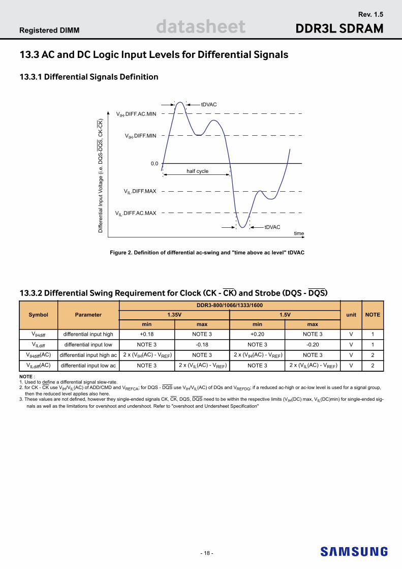
13.3 AC and DC Logic Input Levels for Differential Signals
13.3.1 Differential Signals Definition
Figure 2. Definition of differential ac-swing and "time above ac level" tDVAC
13.3.2 Differential Swing Requirement for Clock (CK - CK) and Strobe (DQS - DQS)
NOTE :1. Used to define a differential signal slew-rate.2. for CK - CK use VIH/VIL(AC) of ADD/CMD and VREFCA; for DQS - DQS use VIH/VIL(AC) of DQs and VREFDQ; if a reduced ac-high or ac-low level is used for a signal group,
then the reduced level applies also here.3. These values are not defined, however they single-ended signals CK, CK, DQS, DQS need to be within the respective limits (VIH(DC) max, VIL(DC)min) for single-ended sig-
nals as well as the limitations for overshoot and undershoot. Refer to "overshoot and Undersheet Specification"
Symbol Parameter
DDR3-800/1066/1333/1600
unit NOTE1.35V 1.5V
min max min max
VIHdiff differential input high +0.18 NOTE 3 +0.20 NOTE 3 V 1
VILdiff differential input low NOTE 3 -0.18 NOTE 3 -0.20 V 1
VIHdiff(AC) differential input high ac 2 x (VIH(AC) - VREF) NOTE 3 2 x (VIH(AC) - VREF) NOTE 3 V 2
VILdiff(AC) differential input low ac NOTE 3 2 x (VIL(AC) - VREF) NOTE 3 2 x (VIL(AC) - VREF) V 2
0.0
tDVAC
VIH.DIFF.MIN
half cycle
Diff
eren
tial I
nput
Vol
tage
(i.e
. DQ
S-D
QS
, CK
-CK
)
timetDVAC
VIH.DIFF.AC.MIN
VIL.DIFF.MAX
VIL.DIFF.AC.MAX

- 19 -
datasheet DDR3L SDRAMRev. 1.5
Registered DIMM
[ Table 6 ] Allowed time before ringback (tDVAC) for CK - CK and DQS - DQS (1.35V)
NOTE: Rising input signal shall become equal to or greater than VIH(ac) level and Falling input signal shall become equal to or less than VIL(ac) level.
[ Table 7 ] Allowed time before ringback (tDVAC) for CK - CK and DQS - DQS (1.5V)
NOTE: Rising input differential signal shall become equal to or greater than VIHdiff(ac) level and Falling input differential signal shall become equal to or less than VILdiff(ac) level
13.3.3 Single-ended Requirements for Differential Signals
Each individual component of a differential signal (CK, DQS, CK, DQS) has also to comply with certain requirements for single-ended signals.CK and CK have to approximately reach VSEHmin / VSELmax (approximately equal to the ac-levels ( VIH(AC) / VIL(AC) ) for ADD/CMD signals) in every
half-cycle. DQS, DQS have to reach VSEHmin / VSELmax (approximately the ac-levels ( VIH(AC) / VIL(AC) ) for DQ signals) in every half-cycle proceeding and follow-
ing a valid transition. Note that the applicable ac-levels for ADD/CMD and DQ’s might be different per speed-bin etc. E.g. if VIH150(AC)/VIL150(AC) is used for ADD/CMD
signals, then these ac-levels apply also for the single-ended signals CK and CK .
Slew Rate [V/ns]
DDR3L-800/1066/1333/1600
tDVAC [ps] @ |VIH/Ldiff(AC)| = 320mV tDVAC [ps] @ |VIH/Ldiff(AC)| = 270mV
min max min max
> 4.0 189 - 201 -
4.0 189 - 201 -
3.0 162 - 179 -
2.0 109 - 134 -
1.8 91 - 119 -
1.6 69 - 100 -
1.4 40 - 76 -
1.2 note - 44 -
1.0 note - note -
< 1.0 note - note -
Slew Rate [V/ns]
DDR3-800/1066/1333/1600
tDVAC [ps] @ |VIH/Ldiff(AC)| = 350mV
tDVAC [ps] @ |VIH/Ldiff(AC)| = 300mV
tDVAC [ps] @ |VIH/Ldiff(AC)| = (DQS-DQS#)only(Optional)
min max min max min max
> 4.0 75 - 175 - 214 -
4.0 57 - 170 - 214 -
3.0 50 - 167 - 191 -
2.0 38 - 119 - 146 -
1.8 34 - 102 - 131 -
1.6 29 - 81 - 113 -
1.4 22 - 54 - 88 -
1.2 note - 19 - 56 -
1.0 note - note - 11 -
< 1.0 note - note - note -
- 20 -
datasheet DDR3L SDRAMRev. 1.5
Registered DIMM
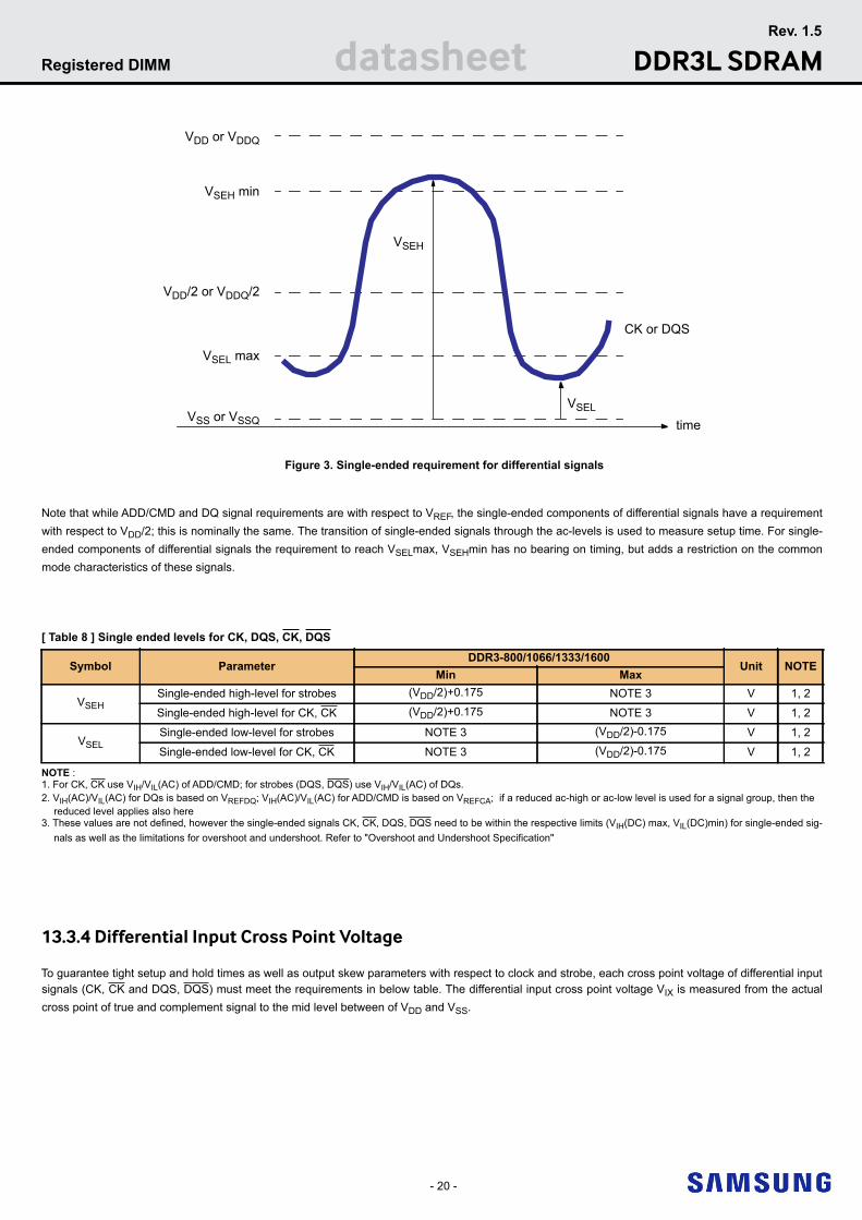
Figure 3. Single-ended requirement for differential signals
Note that while ADD/CMD and DQ signal requirements are with respect to VREF, the single-ended components of differential signals have a requirement with respect to VDD/2; this is nominally the same. The transition of single-ended signals through the ac-levels is used to measure setup time. For single-ended components of differential signals the requirement to reach VSELmax, VSEHmin has no bearing on timing, but adds a restriction on the common mode characteristics of these signals.
[ Table 8 ] Single ended levels for CK, DQS, CK, DQS
NOTE :1. For CK, CK use VIH/VIL(AC) of ADD/CMD; for strobes (DQS, DQS) use VIH/VIL(AC) of DQs.2. VIH(AC)/VIL(AC) for DQs is based on VREFDQ; VIH(AC)/VIL(AC) for ADD/CMD is based on VREFCA; if a reduced ac-high or ac-low level is used for a signal group, then the
reduced level applies also here3. These values are not defined, however the single-ended signals CK, CK, DQS, DQS need to be within the respective limits (VIH(DC) max, VIL(DC)min) for single-ended sig-
nals as well as the limitations for overshoot and undershoot. Refer to "Overshoot and Undershoot Specification"
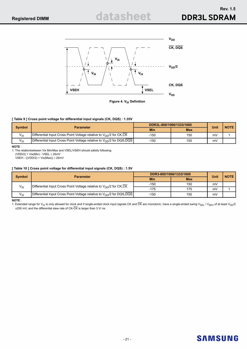
13.3.4 Differential Input Cross Point Voltage
To guarantee tight setup and hold times as well as output skew parameters with respect to clock and strobe, each cross point voltage of differential input signals (CK, CK and DQS, DQS) must meet the requirements in below table. The differential input cross point voltage VIX is measured from the actual cross point of true and complement signal to the mid level between of VDD and VSS.
Symbol ParameterDDR3-800/1066/1333/1600
Unit NOTEMin Max
VSEHSingle-ended high-level for strobes (VDD/2)+0.175 NOTE 3 V 1, 2
Single-ended high-level for CK, CK (VDD/2)+0.175 NOTE 3 V 1, 2
VSELSingle-ended low-level for strobes NOTE 3 (VDD/2)-0.175 V 1, 2
Single-ended low-level for CK, CK NOTE 3 (VDD/2)-0.175 V 1, 2
VDD or VDDQ
VSEH min
VDD/2 or VDDQ/2
VSEL max
VSEH
VSS or VSSQVSEL
CK or DQS
time
- 21 -
datasheet DDR3L SDRAMRev. 1.5
Registered DIMM
Figure 4. VIX Definition
[ Table 9 ] Cross point voltage for differential input signals (CK, DQS) : 1.35V
NOTE : 1. The relationbetween Vix Min/Max and VSEL/VSEH should satisfy following.
(VDD/2) + Vix(Min) - VSEL 25mVVSEH - ((VDD/2) + Vix(Max)) 25mV
[ Table 10 ] Cross point voltage for differential input signals (CK, DQS) : 1.5V
NOTE : 1. Extended range for VIX is only allowed for clock and if single-ended clock input signals CK and CK are monotonic, have a single-ended swing VSEL / VSEH of at least VDD/2
±250 mV, and the differential slew rate of CK-CK is larger than 3 V/ ns.
Symbol ParameterDDR3L-800/1066/1333/1600
Unit NOTEMin Max
VIX Differential Input Cross Point Voltage relative to VDD/2 for CK,CK -150 150 mV 1VIX Differential Input Cross Point Voltage relative to VDD/2 for DQS,DQS -150 150 mV
Symbol ParameterDDR3-800/1066/1333/1600
Unit NOTEMin Max
VIX Differential Input Cross Point Voltage relative to VDD/2 for CK,CK -150 150 mV-175 175 mV 1
VIX Differential Input Cross Point Voltage relative to VDD/2 for DQS,DQS -150 150 mV
VDD
CK, DQS
VDD/2
CK, DQS
VSS
VIX
VIX
VIX
VSEH VSEL

- 22 -
datasheet DDR3L SDRAMRev. 1.5
Registered DIMM
13.4 Slew Rate Definition for Single Ended Input SignalsSee "Address / Command Setup, Hold and Derating" for single-ended slew rate definitions for address and command signals.See "Data Setup, Hold and Slew Rate Derating" for single-ended slew rate definitions for data signals.
13.5 Slew Rate Definition for Differential Input SignalsInput slew rate for differential signals (CK, CK and DQS, DQS) are defined and measured as shown in below.
[ Table 11 ] Differential input slew rate definition
NOTE : The differential signal (i.e. CK - CK and DQS - DQS) must be linear between these thresholds
Figure 5. Differential input slew rate definition for DQS, DQS and CK, CK
14. AC & DC Output Measurement Levels
14.1 Single Ended AC and DC Output Levels[ Table 12 ] Single Ended AC and DC output levels
NOTE : 1. The swing of +/-0.1 x VDDQ is based on approximately 50% of the static single ended output high or low swing with a driver impedance of 40 and an effective test load of 25 to VTT=VDDQ/2.
14.2 Differential AC and DC Output Levels[ Table 13 ] Differential AC and DC output levels
NOTE : 1. The swing of +/-0.2xVDDQ is based on approximately 50% of the static single ended output high or low swing with a driver impedance of 40 and an effective test load of 25 to VTT=VDDQ/2 at each of the differential outputs.
DescriptionMeasured
Defined byFrom To
Differential input slew rate for rising edge (CK-CK and DQS-DQS) VILdiffmax VIHdiffmin [VIHdiffmin - VILdiffmax] / Delta TRdiff
Differential input slew rate for falling edge (CK-CK and DQS-DQS) VIHdiffmin VILdiffmax [VIHdiffmin - VILdiffmax] / Delta TFdiff
Symbol Parameter DDR3-800/1066/1333/1600 Units NOTE
VOH(DC) DC output high measurement level (for IV curve linearity) 0.8 x VDDQ V
VOM(DC) DC output mid measurement level (for IV curve linearity) 0.5 x VDDQ V
VOL(DC) DC output low measurement level (for IV curve linearity) 0.2 x VDDQ V
VOH(AC) AC output high measurement level (for output SR) VTT + 0.1 x VDDQ V 1
VOL(AC) AC output low measurement level (for output SR) VTT - 0.1 x VDDQ V 1
Symbol Parameter DDR3-800/1066/1333/1600 Units NOTE
VOHdiff(AC) AC differential output high measurement level (for output SR) +0.2 x VDDQ V 1
VOLdiff(AC) AC differential output low measurement level (for output SR) -0.2 x VDDQ V 1
VIHdiffmin
0
VILdiffmax
delta TRdiffdelta TFdiff

- 23 -
datasheet DDR3L SDRAMRev. 1.5
Registered DIMM
14.3 Single-ended Output Slew RateWith the reference load for timing measurements, output slew rate for falling and rising edges is defined and measured between VOL(AC) and VOH(AC)
for single ended signals as shown in below.[ Table 14 ] Single ended Output slew rate definition
NOTE : Output slew rate is verified by design and characterization, and may not be subject to production test.
[ Table 15 ] Single ended output slew rate
Description : SR : Slew RateQ : Query Output (like in DQ, which stands for Data-in, Query-Output)se : Single-ended SignalsFor Ron = RZQ/7 settingNOTE : 1) In two cased, a maximum slew rate of 6V/ns applies for a single DQ signal within a byte lane.
- Case_1 is defined for a single DQ signal within a byte lane which is switching into a certain direction (either from high to low of low to high) while all remaining DQ signals in the same byte lane are static (i.e they stay at either high or low).
- Case_2 is defined for a single DQ signals in the same byte lane are switching into the opposite direction (i.e. from low to high or high to low respectively). For the remaining DQ signal switching into the opposite direction, the regular maximum limit of 5 V/ns applies.
Figure 6. Single-ended output slew rate definition
DescriptionMeasured
Defined byFrom To
Single ended output slew rate for rising edge VOL(AC) VOH(AC) [VOH(AC)-VOL(AC)] / Delta TRse
Single ended output slew rate for falling edge VOH(AC) VOL(AC) [VOH(AC)-VOL(AC)] / Delta TFse
Parameter Symbol OperationVoltage
DDR3-800 DDR3-1066 DDR3-1333 DDR3-1600Units
Min Max Min Max Min Max Min Max
Single ended output slew rate SRQse1.35V 1.75 51) 1.75 51) 1.75 51) 1.75 51) V/ns
1.5V 2.5 5 2.5 5 2.5 5 2.5 5 V/ns
VOHdiff(AC)
VOLdiff(AC)
delta TRdiffdelta TFdiff
VTT

- 24 -
datasheet DDR3L SDRAMRev. 1.5
Registered DIMM
14.4 Differential Output Slew RateWith the reference load for timing measurements, output slew rate for falling and rising edges is defined and measured between VOLdiff(AC) and
VOHdiff(AC) for differential signals as shown in below.
[ Table 16 ] Differential Output slew rate definition
NOTE : Output slew rate is verified by design and characterization, and may not be subject to production test.
[ Table 17 ] Differential Output slew rate
Description : SR : Slew RateQ : Query Output (like in DQ, which stands for Data-in, Query-Output)diff : Differential SignalsFor Ron = RZQ/7 setting
Figure 7. Differential output slew rate definition
DescriptionMeasured
Defined byFrom To
Differential output slew rate for rising edge VOLdiff(AC) VOHdiff(AC) [VOHdiff(AC)-VOLdiff(AC)] / Delta TRdiff
Differential output slew rate for falling edge VOHdiff(AC) VOLdiff(AC) [VOHdiff(AC)-VOLdiff(AC)]/ Delta TFdiff
Parameter Symbol OperationVoltage
DDR3-800 DDR3-1066 DDR3-1333 DDR3-1600Units
Min Max Min Max Min Max Min Max
Differential output slew rate SRQdiff1.35V 3.5 12 3.5 12 3.5 12 3.5 12 V/ns
1.5V 5 10 5 10 5 10 5 10 V/ns
VOHdiff(AC)
VOLdiff(AC)
delta TRdiffdelta TFdiff
VTT

- 25 -
datasheet DDR3L SDRAMRev. 1.5
Registered DIMM
15. IDD specification definitionSymbol Description
IDD0
Operating One Bank Active-Precharge CurrentCKE: High; External clock: On; tCK, nRC, nRAS, CL: Refer to Component Datasheet for detail pattern ; BL: 81); AL: 0; CS: High between ACT and PRE; Command, Address, Bank Address Inputs: partially toggling ; Data IO: FLOATING; DM:stable at 0; Bank Activity: Cycling with one bank active at a time: 0,0,1,1,2,2,... ; Output Buffer and RTT: Enabled in Mode Registers2); ODT Signal: stable at 0; Pattern Details: Refer to Component Datasheet for detail pat-tern
IDD1
Operating One Bank Active-Read-Precharge CurrentCKE: High; External clock: On; tCK, nRC, nRAS, nRCD, CL: Refer to Component Datasheet for detail pattern ; BL: 81); AL: 0; CS: High between ACT, RD and PRE; Command, Address, Bank Address Inputs, Data IO: partially toggling ; DM:stable at 0; Bank Activity: Cycling with one bank active at a time: 0,0,1,1,2,2,... ; Output Buffer and RTT: Enabled in Mode Registers2); ODT Signal: stable at 0; Pattern Details: Refer to Component Datasheet for detail pat-tern
IDD2N
Precharge Standby CurrentCKE: High; External clock: On; tCK, CL: Refer to Component Datasheet for detail pattern ; BL: 81); AL: 0; CS: stable at 1; Command, Address, Bank Address Inputs: partially toggling ; Data IO: FLOATING; DM:stable at 0; Bank Activity: all banks closed; Output Buffer and RTT: Enabled in Mode Regis-ters2); ODT Signal: stable at 0; Pattern Details: Refer to Component Datasheet for detail pattern
IDD2P0
Precharge Power-Down Current Slow ExitCKE: Low; External clock: On; tCK, CL: Refer to Component Datasheet for detail pattern ; BL: 81); AL: 0; CS: stable at 1; Command, Address, Bank Address Inputs: stable at 0; Data IO: FLOATING; DM:stable at 0; Bank Activity: all banks closed; Output Buffer and RTT: Enabled in Mode Registers2); ODT Signal: stable at 0; Precharge Power Down Mode: Slow Exit3)
IDD2P1
Precharge Power-Down Current Fast ExitCKE: Low; External clock: On; tCK, CL: Refer to Component Datasheet for detail pattern ; BL: 81); AL: 0; CS: stable at 1; Command, Address, Bank Address Inputs: stable at 0; Data IO: FLOATING; DM:stable at 0; Bank Activity: all banks closed; Output Buffer and RTT: Enabled in Mode Registers2); ODT Signal: stable at 0; Precharge Power Down Mode: Fast Exit3)
IDD2Q
Precharge Quiet Standby CurrentCKE: High; External clock: On; tCK, CL: Refer to Component Datasheet for detail pattern ; BL: 81); AL: 0; CS: stable at 1; Command, Address, Bank Address Inputs: stable at 0; Data IO: FLOATING; DM:stable at 0;Bank Activity: all banks closed; Output Buffer and RTT: Enabled in Mode Registers2); ODT Signal: stable at 0
IDD3N
Active Standby CurrentCKE: High; External clock: On; tCK, CL: Refer to Component Datasheet for detail pattern ; BL: 81); AL: 0; CS: stable at 1; Command, Address, Bank Address Inputs: partially toggling ; Data IO: FLOATING; DM:stable at 0;Bank Activity: all banks open; Output Buffer and RTT: Enabled in Mode Registers2); ODT Signal: stable at 0; Pattern Details: Refer to Component Datasheet for detail pattern
IDD3P
Active Power-Down CurrentCKE: Low; External clock: On; tCK, CL: Refer to Component Datasheet for detail pattern ; BL: 81); AL: 0; CS: stable at 1; Command, Address, Bank Address Inputs: stable at 0; Data IO: FLOATING;DM:stable at 0; Bank Activity: all banks open; Output Buffer and RTT: Enabled in Mode Registers2); ODT Signal: stable at 0
IDD4R
Operating Burst Read CurrentCKE: High; External clock: On; tCK, CL: Refer to Component Datasheet for detail pattern ; BL: 81); AL: 0; CS: High between RD; Command, Address, Bank Address Inputs: partially toggling ; Data IO: seamless read data burst with different data between one burst and the next one ; DM:stable at 0; Bank Activity: all banks open, RD commands cycling through banks: 0,0,1,1,2,2,... ; Output Buffer and RTT: Enabled in Mode Registers2); ODT Signal: stable at 0; Pattern Details: Refer to Component Datasheet for detail pattern
IDD4W
Operating Burst Write CurrentCKE: High; External clock: On; tCK, CL: Refer to Component Datasheet for detail pattern ; BL: 81); AL: 0; CS: High between WR; Command, Address, Bank Address Inputs: partially toggling ; Data IO: seamless write data burst with different data between one burst and the next one ; DM: stable at 0; Bank Activity: all banks open, WR commands cycling through banks: 0,0,1,1,2,2,... ; Output Buffer and RTT: Enabled in Mode Registers2); ODT Signal: stable at HIGH; Pattern Details: Refer to Component Datasheet for detail pattern
IDD5B
Burst Refresh CurrentCKE: High; External clock: On; tCK, CL, nRFC: Refer to Component Datasheet for detail pattern ; BL: 81); AL: 0; CS: High between REF; Command, Address, Bank Address Inputs: partially toggling ; Data IO: FLOATING;DM:stable at 0; Bank Activity: REF command every nRFC ; Output Buffer and RTT: Enabled in Mode Registers2); ODT Signal: stable at 0; Pattern Details: Refer to Component Datasheet for detail pattern
IDD6
Self Refresh Current: Normal Temperature RangeTCASE: 0 - 85°C; Auto Self-Refresh (ASR): Disabled4); Self-Refresh Temperature Range (SRT): Normal5); CKE: Low; External clock: Off; CK and CK: LOW; CL: Refer to Component Datasheet for detail pattern ; BL: 81); AL: 0; CS, Command, Address, Bank Address, Data IO: FLOATING;DM:stable at 0; Bank Activity: Self-Refresh operation; Output Buffer and RTT: Enabled in Mode Registers2); ODT Signal: FLOATING
IDD6ET
Self-Refresh Current: Extended Temperature Range (optional)6)
TCASE: 0 - 95°C; Auto Self-Refresh (ASR): Disabled4); Self-Refresh Temperature Range (SRT): Extended5); CKE: Low; External clock: Off; CK and CK: LOW; CL: Refer to Component Datasheet for detail pattern ; BL: 81); AL: 0; CS, Command, Address, Bank Address, Data IO: FLOATING;DM:stable at 0; Bank Activity: Extended Temperature Self-Refresh operation; Output Buffer and RTT: Enabled in Mode Registers2); ODT Signal: FLOATING
IDD7
Operating Bank Interleave Read CurrentCKE: High; External clock: On; tCK, nRC, nRAS, nRCD, nRRD, nFAW, CL: Refer to Component Datasheet for detail pattern ; BL: 81); AL: CL-1; CS: High between ACT and RDA; Command, Address, Bank Address Inputs: partially toggling ; Data IO: read data bursts with different data between one burst and the next one ; DM:stable at 0; Bank Activity: two times interleaved cycling through banks (0, 1, ...7) with different addressing ; Output Buffer and RTT: Enabled in Mode Registers2); ODT Signal: stable at 0; Pattern Details: Refer to Component Datasheet for detail pattern
IDD8RESET Low CurrentRESET : Low; External clock : off; CK and CK : LOW; CKE : FLOATING ; CS, Command, Address, Bank Address, Data IO : FLOATING ; ODT Signal : FLOATING

- 26 -
datasheet DDR3L SDRAMRev. 1.5
Registered DIMM
NOTE :1) Burst Length: BL8 fixed by MRS: set MR0 A[1,0]=00B2) Output Buffer Enable: set MR1 A[12] = 0B; set MR1 A[5,1] = 01B; RTT_Nom enable: set MR1 A[9,6,2] = 011B; RTT_Wr enable: set MR2 A[10,9] = 10B3) Precharge Power Down Mode: set MR0 A12=0B for Slow Exit or MR0 A12=1B for Fast Exit4) Auto Self-Refresh (ASR): set MR2 A6 = 0B to disable or 1B to enable feature5) Self-Refresh Temperature Range (SRT): set MR2 A7=0B for normal or 1B for extended temperature range6) Refer to DRAM supplier data sheet and/or DIMM SPD to determine if optional features or requirements are supported by DDR3 SDRAM device7) IDD current measure method and detail patterns are described on DDR3 component datasheet8) VDD and VDDQ are merged on module PCB.9) DIMM IDD SPEC is measured with Qoff condition (IDDQ values are not considered)

- 27 -
datasheet DDR3L SDRAMRev. 1.5
Registered DIMM
16. IDD SPEC Table
M393B1G70EB0 : 8GB(1Gx72) Module
M393B1G73EB0 : 8GB(1Gx72) Module
NOTE :1. DIMM IDD SPEC is calculated with considering de-actived rank(IDLE) is IDD2N.
SymbolDDR3-1600
Unit NOTE11-11-111.35V
IDD0 1050 mAIDD1 1230 mA
IDD2P0(slow exit) 550 mAIDD2P1(fast exit) 550 mA
IDD2N 750 mAIDD2Q 890 mAIDD3P 880 mAIDD3N 930 mAIDD4R 1700 mAIDD4W 1700 mAIDD5B 3960 mAIDD6 460 mAIDD7 2640 mAIDD8 550 mA
SymbolDDR3-1600
Unit NOTE11-11-111.35V
IDD0 870 mA 1IDD1 950 mA 1
IDD2P0(slow exit) 390 mAIDD2P1(fast exit) 390 mA
IDD2N 730 mAIDD2Q 690 mAIDD3P 680 mAIDD3N 890 mAIDD4R 1150 mA 1IDD4W 1160 mA 1IDD5B 2150 mA 1IDD6 220 mAIDD7 1560 mA 1IDD8 550 mA

- 28 -
datasheet DDR3L SDRAMRev. 1.5
Registered DIMM
M393B2G70EB0 : 16GB(2Gx72) Module
NOTE :1. DIMM IDD SPEC is calculated with considering de-actived rank(IDLE) is IDD2N.
SymbolDDR3-1600
Unit NOTE11-11-111.35V
IDD0 1240 mA 1IDD1 1420 mA 1
IDD2P0(slow exit) 550 mAIDD2P1(fast exit) 550 mA
IDD2N 950 mAIDD2Q 890 mAIDD3P 880 mAIDD3N 1130 mAIDD4R 1890 mA 1IDD4W 1890 mA 1IDD5B 4160 mA 1IDD6 460 mAIDD7 2830 mA 1IDD8 550 mA

- 29 -
datasheet DDR3L SDRAMRev. 1.5
Registered DIMM
17. Input/Output Capacitance[ Table 18 ] Input/Output Capacitance
NOTE : This parameter is Component Input/Output Capacitance so that is different from Module level Capacitance.1. Although the DM, TDQS and TDQS pins have different functions, the loading matches DQ and DQS2. This parameter is not subject to production test. It is verified by design and characterization. The capacitance is measured according to JEP147("PROCEDURE FOR MEASURING INPUT CAPACITANCE USING A VECTOR NETWORK ANALYZER( VNA)") with
VDD, VDDQ, VSS, VSSQ applied and all other pins floating (except the pin under test, CKE, RESET and ODT as necessary). VDD=VDDQ=1.5V or 1.35V, VBIAS=VDD/2 and on-die termination off.
3. This parameter applies to monolithic devices only; stacked/dual-die devices are not covered here4. Absolute value of CCK-CCK5. Absolute value of CIO(DQS)-CIO(DQS)6. CI applies to ODT, CS, CKE, A0-A15, BA0-BA2, RAS, CAS, WE.7. CDI_CTRL applies to ODT, CS and CKE8. CDI_CTRL=CI(CTRL)-0.5*(CI(CLK)+CI(CLK))9. CDI_ADD_CMD applies to A0-A15, BA0-BA2, RAS, CAS and WE10. CDI_ADD_CMD=CI(ADD_CMD) - 0.5*(CI(CLK)+CI(CLK))11. CDIO=CIO(DQ,DM) - 0.5*(CIO(DQS)+CIO(DQS))12. Maximum external load capacitance on ZQ pin: 5pF
Parameter SymbolDDR3-800 DDR3-1066 DDR3-1333 DDR3-1600
Units NOTEMin Max Min Max Min Max Min Max
1.35V
Input/output capacitance(DQ, DM, DQS, DQS, TDQS, TDQS)
CIO 1.4 2.5 1.4 2.5 1.4 2.3 1.4 2.2 pF 1,2,3
Input capacitance(CK and CK)
CCK 0.8 1.6 0.8 1.6 0.8 1.4 0.8 1.4 pF 2,3
Input capacitance delta(CK and CK)
CDCK 0 0.15 0 0.15 0 0.15 0 0.15 pF 2,3,4
Input capacitance(All other input-only pins)
CI 0.75 1.3 0.75 1.3 0.75 1.3 0.75 1.2 pF 2,3,6
Input/Output capacitance delta(DQS and DQS)
CDDQS 0 0.2 0 0.2 0 0.15 0 0.15 pF 2,3,5
Input capacitance delta(All control input-only pins)
CDI_CTRL -0.5 0.3 -0.5 0.3 -0.4 0.2 -0.4 0.2 pF 2,3,7,8
Input capacitance delta(all ADD and CMD input-only pins)
CDI_ADD_CMD -0.5 0.5 -0.5 0.5 -0.4 0.4 -0.4 0.4 pF 2,3,9,10
Input/output capacitance delta(DQ, DM, DQS, DQS, TDQS, TDQS)
CDIO -0.5 0.3 -0.5 0.3 -0.5 0.3 -0.5 0.3 pF 2,3,11
Input/output capacitance of ZQ pin CZQ - 3 - 3 - 3 - 3 pF 2, 3, 12
1.5V
Input/output capacitance(DQ, DM, DQS, DQS, TDQS, TDQS)
CIO 1.4 3.0 1.4 2.7 1.4 2.5 1.4 2.3 pF 1,2,3
Input capacitance(CK and CK)
CCK 0.8 1.6 0.8 1.6 0.8 1.4 0.8 1.4 pF 2,3
Input capacitance delta(CK and CK)
CDCK 0 0.15 0 0.15 0 0.15 0 0.15 pF 2,3,4
Input capacitance(All other input-only pins)
CI 0.75 1.4 0.75 1.35 0.75 1.3 0.75 1.3 pF 2,3,6
Input capacitance delta(DQS and DQS)
CDDQS 0 0.2 0 0.2 0 0.15 0 0.15 pF 2,3,5
Input capacitance delta(All control input-only pins)
CDI_CTRL -0.5 0.3 -0.5 0.3 -0.4 0.2 -0.4 0.2 pF 2,3,7,8
Input capacitance delta(all ADD and CMD input-only pins)
CDI_ADD_CMD -0.5 0.5 -0.5 0.5 -0.4 0.4 -0.4 0.4 pF 2,3,9,10
Input/output capacitance delta(DQ, DM, DQS, DQS, TDQS, TDQS)
CDIO -0.5 0.3 -0.5 0.3 -0.5 0.3 -0.5 0.3 pF 2,3,11
Input/output capacitance of ZQ pin CZQ - 3 - 3 - 3 - 3 pF 2, 3, 12

- 30 -
datasheet DDR3L SDRAMRev. 1.5
Registered DIMM
18. Electrical Characteristics and AC timing [0 C<TCASE 95 C, VDDQ = 1.35V(1.28V~1.45V) & 1.5V(1.425V~1.575V); VDD = 1.35V(1.28V~1.45V) & 1.5V(1.425V~1.575V)]
18.1 Refresh Parameters by Device Density
NOTE :1. Users should refer to the DRAM supplier data sheet and/or the DIMM SPD to determine if DDR3 SDRAM devices support the following options or requirements referred to in
this material.
18.2 Speed Bins and CL, tRCD, tRP, tRC and tRAS for Corresponding Bin
18.3 Speed Bins and CL, tRCD, tRP, tRC and tRAS for Corresponding Bin DDR3 SDRAM Speed Bins include tCK, tRCD, tRP, tRAS and tRC for each corresponding bin.
[ Table 19 ] DDR3-800 Speed Bins
Parameter Symbol 1Gb 2Gb 4Gb 8Gb Units NOTE
All Bank Refresh to active/refresh cmd time tRFC 110 160 260 350 ns
Average periodic refresh interval tREFI0CTCASE 85C 7.8 7.8 7.8 7.8 s
85CTCASE 95C 3.9 3.9 3.9 3.9 s 1
Speed DDR3-800 DDR3-1066 DDR3-1333 DDR3-1600
Units NOTEBin (CL - tRCD - tRP) 6-6-6 7-7-7 9-9-9 11-11-11
Parameter min min min min
CL 6 7 9 11 tCK
tRCD 15 13.13 13.5 13.75 ns
tRP 15 13.13 13.5 13.75 ns
tRAS 37.5 37.5 36 35 ns
tRC 52.5 50.63 49.5 48.75 ns
tRRD 10 7.5 6.0 6.0 ns
tFAW 40 37.5 30 30 ns
Speed DDR3-800
Units NOTECL-nRCD-nRP 6 - 6 - 6
Parameter Symbol min max
Internal read command to first data tAA 15 20 ns
ACT to internal read or write delay time tRCD 15 - ns
PRE command period tRP 15 - ns
ACT to ACT or REF command period tRC 52.5 - ns
ACT to PRE command period tRAS 37.5 9*tREFI ns
CL = 6 / CWL = 5 tCK(AVG) 2.5 3.3 ns 1,2,3
Supported CL Settings 6 nCK
Supported CWL Settings 5 nCK
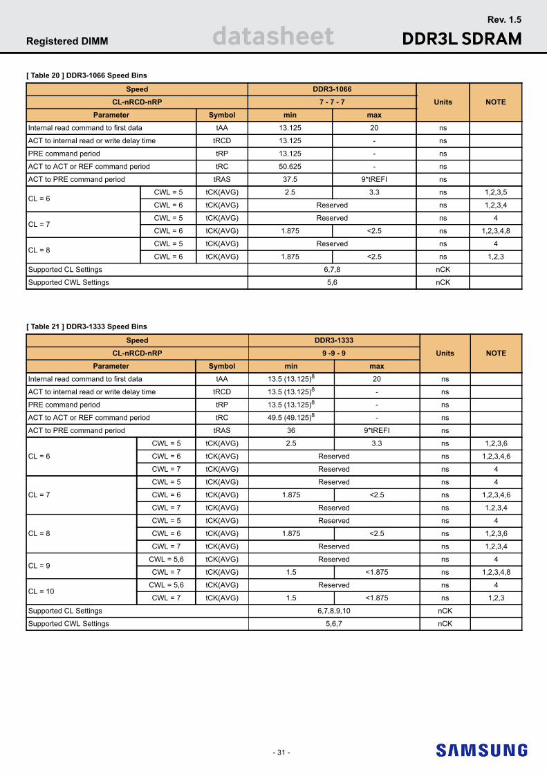
- 31 -
datasheet DDR3L SDRAMRev. 1.5
Registered DIMM
[ Table 20 ] DDR3-1066 Speed Bins
[ Table 21 ] DDR3-1333 Speed Bins
Speed DDR3-1066
Units NOTECL-nRCD-nRP 7 - 7 - 7
Parameter Symbol min max
Internal read command to first data tAA 13.125 20 ns
ACT to internal read or write delay time tRCD 13.125 - ns
PRE command period tRP 13.125 - ns
ACT to ACT or REF command period tRC 50.625 - ns
ACT to PRE command period tRAS 37.5 9*tREFI ns
CL = 6CWL = 5 tCK(AVG) 2.5 3.3 ns 1,2,3,5
CWL = 6 tCK(AVG) Reserved ns 1,2,3,4
CL = 7CWL = 5 tCK(AVG) Reserved ns 4
CWL = 6 tCK(AVG) 1.875 <2.5 ns 1,2,3,4,8
CL = 8CWL = 5 tCK(AVG) Reserved ns 4
CWL = 6 tCK(AVG) 1.875 <2.5 ns 1,2,3
Supported CL Settings 6,7,8 nCK
Supported CWL Settings 5,6 nCK
Speed DDR3-1333
Units NOTECL-nRCD-nRP 9 -9 - 9
Parameter Symbol min max
Internal read command to first data tAA 13.5 (13.125)8 20 ns
ACT to internal read or write delay time tRCD 13.5 (13.125)8 - ns
PRE command period tRP 13.5 (13.125)8 - ns
ACT to ACT or REF command period tRC 49.5 (49.125)8 - ns
ACT to PRE command period tRAS 36 9*tREFI ns
CL = 6
CWL = 5 tCK(AVG) 2.5 3.3 ns 1,2,3,6
CWL = 6 tCK(AVG) Reserved ns 1,2,3,4,6
CWL = 7 tCK(AVG) Reserved ns 4
CL = 7
CWL = 5 tCK(AVG) Reserved ns 4
CWL = 6 tCK(AVG) 1.875 <2.5 ns 1,2,3,4,6
CWL = 7 tCK(AVG) Reserved ns 1,2,3,4
CL = 8
CWL = 5 tCK(AVG) Reserved ns 4
CWL = 6 tCK(AVG) 1.875 <2.5 ns 1,2,3,6
CWL = 7 tCK(AVG) Reserved ns 1,2,3,4
CL = 9CWL = 5,6 tCK(AVG) Reserved ns 4
CWL = 7 tCK(AVG) 1.5 <1.875 ns 1,2,3,4,8
CL = 10CWL = 5,6 tCK(AVG) Reserved ns 4
CWL = 7 tCK(AVG) 1.5 <1.875 ns 1,2,3
Supported CL Settings 6,7,8,9,10 nCK
Supported CWL Settings 5,6,7 nCK
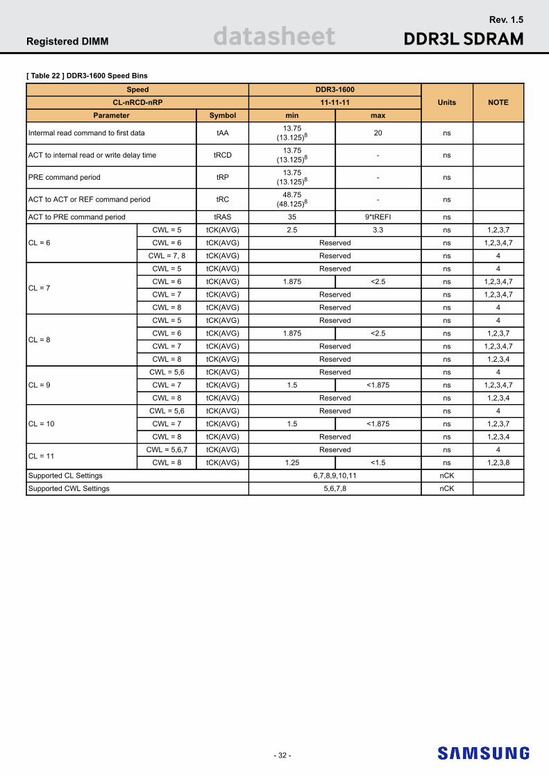
- 32 -
datasheet DDR3L SDRAMRev. 1.5
Registered DIMM
[ Table 22 ] DDR3-1600 Speed Bins
Speed DDR3-1600
Units NOTECL-nRCD-nRP 11-11-11
Parameter Symbol min max
Intermal read command to first data tAA 13.75(13.125)8 20 ns
ACT to internal read or write delay time tRCD 13.75(13.125)8 - ns
PRE command period tRP 13.75(13.125)8 - ns
ACT to ACT or REF command period tRC 48.75(48.125)8 - ns
ACT to PRE command period tRAS 35 9*tREFI ns
CL = 6
CWL = 5 tCK(AVG) 2.5 3.3 ns 1,2,3,7
CWL = 6 tCK(AVG) Reserved ns 1,2,3,4,7
CWL = 7, 8 tCK(AVG) Reserved ns 4
CL = 7
CWL = 5 tCK(AVG) Reserved ns 4
CWL = 6 tCK(AVG) 1.875 <2.5 ns 1,2,3,4,7
CWL = 7 tCK(AVG) Reserved ns 1,2,3,4,7
CWL = 8 tCK(AVG) Reserved ns 4
CL = 8
CWL = 5 tCK(AVG) Reserved ns 4
CWL = 6 tCK(AVG) 1.875 <2.5 ns 1,2,3,7
CWL = 7 tCK(AVG) Reserved ns 1,2,3,4,7
CWL = 8 tCK(AVG) Reserved ns 1,2,3,4
CL = 9
CWL = 5,6 tCK(AVG) Reserved ns 4
CWL = 7 tCK(AVG) 1.5 <1.875 ns 1,2,3,4,7
CWL = 8 tCK(AVG) Reserved ns 1,2,3,4
CL = 10
CWL = 5,6 tCK(AVG) Reserved ns 4
CWL = 7 tCK(AVG) 1.5 <1.875 ns 1,2,3,7
CWL = 8 tCK(AVG) Reserved ns 1,2,3,4
CL = 11CWL = 5,6,7 tCK(AVG) Reserved ns 4
CWL = 8 tCK(AVG) 1.25 <1.5 ns 1,2,3,8
Supported CL Settings 6,7,8,9,10,11 nCK
Supported CWL Settings 5,6,7,8 nCK
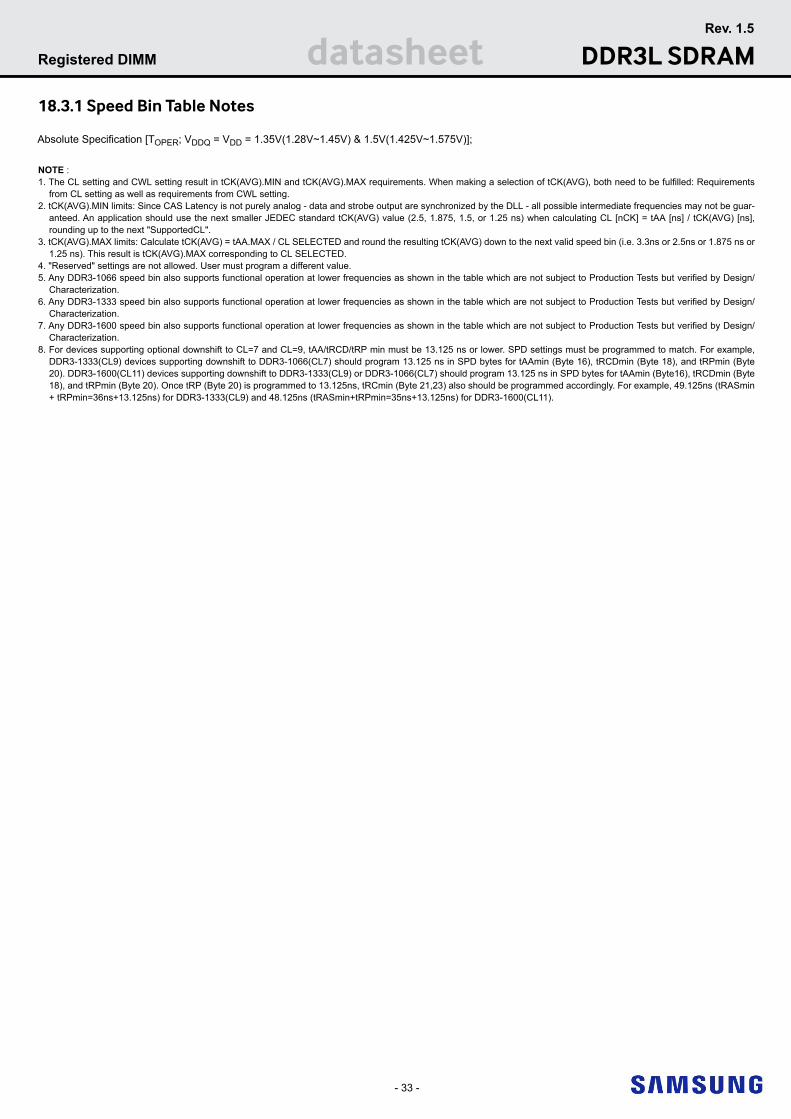
- 33 -
datasheet DDR3L SDRAMRev. 1.5
Registered DIMM
18.3.1 Speed Bin Table Notes
Absolute Specification [TOPER; VDDQ = VDD = 1.35V(1.28V~1.45V) & 1.5V(1.425V~1.575V)];
NOTE :1. The CL setting and CWL setting result in tCK(AVG).MIN and tCK(AVG).MAX requirements. When making a selection of tCK(AVG), both need to be fulfilled: Requirements
from CL setting as well as requirements from CWL setting.2. tCK(AVG).MIN limits: Since CAS Latency is not purely analog - data and strobe output are synchronized by the DLL - all possible intermediate frequencies may not be guar-
anteed. An application should use the next smaller JEDEC standard tCK(AVG) value (2.5, 1.875, 1.5, or 1.25 ns) when calculating CL [nCK] = tAA [ns] / tCK(AVG) [ns], rounding up to the next "SupportedCL".
3. tCK(AVG).MAX limits: Calculate tCK(AVG) = tAA.MAX / CL SELECTED and round the resulting tCK(AVG) down to the next valid speed bin (i.e. 3.3ns or 2.5ns or 1.875 ns or 1.25 ns). This result is tCK(AVG).MAX corresponding to CL SELECTED.
4. "Reserved" settings are not allowed. User must program a different value.5. Any DDR3-1066 speed bin also supports functional operation at lower frequencies as shown in the table which are not subject to Production Tests but verified by Design/
Characterization.6. Any DDR3-1333 speed bin also supports functional operation at lower frequencies as shown in the table which are not subject to Production Tests but verified by Design/
Characterization.7. Any DDR3-1600 speed bin also supports functional operation at lower frequencies as shown in the table which are not subject to Production Tests but verified by Design/
Characterization.8. For devices supporting optional downshift to CL=7 and CL=9, tAA/tRCD/tRP min must be 13.125 ns or lower. SPD settings must be programmed to match. For example,
DDR3-1333(CL9) devices supporting downshift to DDR3-1066(CL7) should program 13.125 ns in SPD bytes for tAAmin (Byte 16), tRCDmin (Byte 18), and tRPmin (Byte 20). DDR3-1600(CL11) devices supporting downshift to DDR3-1333(CL9) or DDR3-1066(CL7) should program 13.125 ns in SPD bytes for tAAmin (Byte16), tRCDmin (Byte 18), and tRPmin (Byte 20). Once tRP (Byte 20) is programmed to 13.125ns, tRCmin (Byte 21,23) also should be programmed accordingly. For example, 49.125ns (tRASmin + tRPmin=36ns+13.125ns) for DDR3-1333(CL9) and 48.125ns (tRASmin+tRPmin=35ns+13.125ns) for DDR3-1600(CL11).

- 34 -
datasheet DDR3L SDRAMRev. 1.5
Registered DIMM
19. Timing Parameters by Speed Grade[ Table 23 ] Timing Parameters by Speed Bin (Cont.)
Speed DDR3-800 DDR3-1066 DDR3-1333 DDR3-1600Units NOTE
Parameter Symbol MIN MAX MIN MAX MIN MAX MIN MAX
Clock Timing
Minimum Clock Cycle Time (DLL off mode) tCK(DLL_OFF) 8 - 8 - 8 - 8 - ns 6
Average Clock Period tCK(avg) See Speed Bins Table ps
Clock Period tCK(abs) tCK(avg)min + tJIT(per)min
tCK(avg)max + tJIT(per)max
tCK(avg)min + tJIT(per)min
tCK(avg)max + tJIT(per)max
tCK(avg)min + tJIT(per)min
tCK(avg)max + tJIT(per)max
tCK(avg)min + tJIT(per)min
tCK(avg)max + tJIT(per)max ps
Average high pulse width tCH(avg) 0.47 0.53 0.47 0.53 0.47 0.53 0.47 0.53 tCK(avg)
Average low pulse width tCL(avg) 0.47 0.53 0.47 0.53 0.47 0.53 0.47 0.53 tCK(avg)
Clock Period Jitter tJIT(per) -100 100 -90 90 -80 80 -70 70 ps
Clock Period Jitter during DLL locking period tJIT(per, lck) -90 90 -80 80 -70 70 -60 60 ps
Cycle to Cycle Period Jitter tJIT(cc) 200 180 160 140 ps
Cycle to Cycle Period Jitter during DLL locking period tJIT(cc, lck) 180 160 140 120 ps
Cumulative error across 2 cycles tERR(2per) - 147 147 - 132 132 - 118 118 -103 103 ps
Cumulative error across 3 cycles tERR(3per) - 175 175 - 157 157 - 140 140 -122 122 ps
Cumulative error across 4 cycles tERR(4per) - 194 194 - 175 175 - 155 155 -136 136 ps
Cumulative error across 5 cycles tERR(5per) - 209 209 - 188 188 - 168 168 -147 147 ps
Cumulative error across 6 cycles tERR(6per) - 222 222 - 200 200 - 177 177 -155 155 ps
Cumulative error across 7 cycles tERR(7per) - 232 232 - 209 209 - 186 186 -163 163 ps
Cumulative error across 8 cycles tERR(8per) - 241 241 - 217 217 - 193 193 -169 169 ps
Cumulative error across 9 cycles tERR(9per) - 249 249 - 224 224 - 200 200 -175 175 ps
Cumulative error across 10 cycles tERR(10per) - 257 257 - 231 231 - 205 205 -180 180 ps
Cumulative error across 11 cycles tERR(11per) - 263 263 - 237 237 - 210 210 -184 184 ps
Cumulative error across 12 cycles tERR(12per) - 269 269 - 242 242 - 215 215 -188 188 ps
Cumulative error across n = 13, 14 ... 49, 50 cycles tERR(nper) tERR(nper)min = (1 + 0.68ln(n))*tJIT(per)mintERR(nper)max = (1 + 0.68ln(n))*tJIT(per)max ps 24
Absolute clock HIGH pulse width tCH(abs) 0.43 - 0.43 - 0.43 - 0.43 - tCK(avg) 25
Absolute clock Low pulse width tCL(abs) 0.43 - 0.43 - 0.43 - 0.43 - tCK(avg) 26
Data Timing
DQS,DQS to DQ skew, per group, per access tDQSQ - 200 - 150 - 125 - 100 ps 13
DQ output hold time from DQS, DQS tQH 0.38 - 0.38 - 0.38 - 0.38 - tCK(avg) 13, g
DQ low-impedance time from CK, CK tLZ(DQ) -800 400 -600 300 -500 250 -450 225 ps 13,14, f
DQ high-impedance time from CK, CK tHZ(DQ) - 400 - 300 - 250 - 225 ps 13,14, f
Data setup time to DQS, DQS referenced to VIH(AC)VIL(AC) levels
1.35V
tDS(base)AC160 90 - 40 - - - - - ps
d, 17tDS(base)
AC135 140 - 90 - 45 - 25 - ps
1.5V
tDS(base)AC175 75 - 25 - - - - - ps
d, 17tDS(base)
AC150 125 - 75 - 30 - 10 - ps
Data hold time from DQS, DQS referenced to VIH(DC)VIL(DC) levels
1.35V
tDH(base)DC90 160 - 110 - 75 - 55 - ps d, 17
1.5V
tDH(base)DC100 150 - 100 - 65 - 45 - ps d, 17
DQ and DM Input pulse width for each input tDIPW 600 - 490 - 400 - 360 - ps 28

- 35 -
datasheet DDR3L SDRAMRev. 1.5
Registered DIMM
[ Table 24 ] Timing Parameters by Speed Bin (Cont.)Speed DDR3-800 DDR3-1066 DDR3-1333 DDR3-1600
Units NOTEParameter Symbol MIN MAX MIN MAX MIN MAX MIN MAX
Data Strobe Timing
DQS, DQS differential READ Preamble tRPRE 0.9 Note 19 0.9 Note 19 0.9 Note 19 0.9 Note 19 tCK(avg) 13, 19, g
DQS, DQS differential READ Postamble tRPST 0.3 Note 11 0.3 Note 11 0.3 Note 11 0.3 Note 11 tCK(avg) 11, 13, b
DQS, DQS differential output high time tQSH 0.38 - 0.38 - 0.4 - 0.4 - tCK(avg) 13, g
DQS, DQS differential output low time tQSL 0.38 - 0.38 - 0.4 - 0.4 - tCK(avg) 13, g
DQS, DQS differential WRITE Preamble tWPRE 0.9 - 0.9 - 0.9 - 0.9 - tCK(avg)
DQS, DQS differential WRITE Postamble tWPST 0.3 - 0.3 - 0.3 - 0.3 - tCK(avg)
DQS, DQS rising edge output access time from rising CK, CK tDQSCK -400 400 -300 300 -255 255 -225 225 ps 13,f
DQS, DQS low-impedance time (Referenced from RL-1) tLZ(DQS) -800 400 -600 300 -500 250 -450 225 ps 13,14,f
DQS, DQS high-impedance time (Referenced from RL+BL/2) tHZ(DQS) - 400 - 300 - 250 - 225 ps 12,13,14
DQS, DQS differential input low pulse width tDQSL 0.45 0.55 0.45 0.55 0.45 0.55 0.45 0.55 tCK(avg) 29, 31
DQS, DQS differential input high pulse width tDQSH 0.45 0.55 0.45 0.55 0.45 0.55 0.45 0.55 tCK(avg) 30, 31
DQS, DQS rising edge to CK, CK rising edge tDQSS -0.25 0.25 -0.25 0.25 -0.25 0.25 -0.27 0.27 tCK(avg) c
DQS,DQS falling edge setup time to CK, CK rising edge tDSS 0.2 - 0.2 - 0.2 - 0.18 - tCK(avg) c, 32
DQS,DQS falling edge hold time to CK, CK rising edge tDSH 0.2 - 0.2 - 0.2 - 0.18 - tCK(avg) c, 32
Command and Address Timing
DLL locking time tDLLK 512 - 512 - 512 - 512 - nCK
internal READ Command to PRECHARGE Command delay tRTP max
(4nCK,7.5ns) - max(4nCK,7.5ns) - max
(4nCK,7.5ns) - max(4nCK,7.5ns) - e
Delay from start of internal write transaction to internal read command tWTR max
(4nCK,7.5ns) - max(4nCK,7.5ns) - max
(4nCK,7.5ns) - max(4nCK,7.5ns) - e,18
WRITE recovery time tWR 15 - 15 - 15 - 15 - ns e
Mode Register Set command cycle time tMRD 4 - 4 - 4 - 4 - nCK
Mode Register Set command update delay tMOD max(12nCK,15ns) - max
(12nCK,15ns) - max(12nCK,15ns) - max
(12nCK,15ns) -
CAS to CAS command delay tCCD 4 - 4 - 4 - 4 - nCK
Auto precharge write recovery + precharge time tDAL(min) WR + roundup (tRP / tCK(AVG)) nCK
Multi-Purpose Register Recovery Time tMPRR 1 - 1 - 1 - 1 - nCK 22
ACTIVE to PRECHARGE command period tRAS See “Speed Bins and CL, tRCD, tRP, tRC and tRAS for corresponding Bin” ns e
ACTIVE to ACTIVE command period for 1KB page size tRRD max(4nCK,10ns) - max
(4nCK,7.5ns) - max(4nCK,6ns) - max
(4nCK,6ns) - e
ACTIVE to ACTIVE command period for 2KB page size tRRD max(4nCK,10ns) - max
(4nCK,10ns) - max(4nCK,7.5ns) - max
(4nCK,7.5ns) - e
Four activate window for 1KB page size tFAW 40 - 37.5 - 30 - 30 - ns e
Four activate window for 2KB page size tFAW 50 - 50 - 45 - 40 - ns e
Command and Address setup time to CK, CK refer-enced to VIH(AC) / VIL(AC) levels
1.35V
tIS(base)AC160 215 - 140 - 80 - 60 - ps b,16
tIS(base)AC135 365 - 290 - 205 - 185 - ps b,16,27
1.5V
tIS(base)AC175 200 - 125 - 65 - 45 - ps b,16
tIS(base)AC150 350 - 275 - 190 - 170 - ps b,16,27
Command and Address hold time from CK, CK refer-enced to VIH(DC) / VIL(DC) levels
1.35V
tIH(base)DC90 285 - 210 - 150 - 130 - ps b,16
1.5V
tIH(base)DC100 275 200 140 120 - ps b,16
Control & Address Input pulse width for each input tIPW 900 - 780 - 620 - 560 - ps 28
Calibration Timing
Power-up and RESET calibration time tZQinitI 512 - 512 - 512 - 512 - nCK
Normal operation Full calibration time tZQoper 256 - 256 - 256 - 256 - nCK
Normal operation short calibration time tZQCS 64 - 64 - 64 - 64 - nCK 23

- 36 -
datasheet DDR3L SDRAMRev. 1.5
Registered DIMM
[ Table 24 ] Timing Parameters by Speed BinSpeed DDR3-800 DDR3-1066 DDR3-1333 DDR3-1600
Units NOTEParameter Symbol MIN MAX MIN MAX MIN MAX MIN MAX
Reset Timing
Exit Reset from CKE HIGH to a valid command tXPRmax(5nCK,
tRFC + 10ns)
-max(5nCK,
tRFC + 10ns)
-max(5nCK,
tRFC + 10ns)
-max(5nCK,
tRFC + 10ns)
-
Self Refresh Timing
Exit Self Refresh to commands not requiring a locked DLL tXS
max(5nCK,tRFC + 10ns)
-max(5nCK,t
RFC + 10ns)
-max(5nCK,t
RFC + 10ns)
- max(5nCK,tRFC + 10ns) -
Exit Self Refresh to commands requiring a locked DLL tXSDLL tDLLK(min) - tDLLK(min) - tDLLK(min) - tDLLK(min) - nCK
Minimum CKE low width for Self refresh entry to exit timing tCKESR tCKE(min) +
1tCK - tCKE(min) + 1tCK - tCKE(min) +
1tCK - tCKE(min) + 1tCK -
Valid Clock Requirement after Self Refresh Entry (SRE) or Power-Down Entry (PDE) tCKSRE max(5nCK,
10ns) - max(5nCK,10ns) - max(5nCK,
10ns) - max(5nCK,10ns) -
Valid Clock Requirement before Self Refresh Exit (SRX) or Power-Down Exit (PDX) or Reset Exit tCKSRX max(5nCK,
10ns) - max(5nCK,10ns) - max(5nCK,
10ns) - max(5nCK,10ns) -
Power Down Timing
Exit Power Down with DLL on to any valid com-mand;Exit Precharge Power Down with DLLfrozen to commands not requiring a locked DLL
tXPmax
(3nCK,7.5ns)
-max
(3nCK,7.5ns)
- max(3nCK,6ns) - max
(3nCK,6ns) -
Exit Precharge Power Down with DLL frozen to com-mands requiring a locked DLL tXPDLL
max(10nCK,
24ns)-
max(10nCK,
24ns)-
max(10nCK,
24ns)-
max(10nCK,
24ns)- 2
CKE minimum pulse width tCKEmax
(3nCK,7.5ns)
-max
(3nCK,5.625ns)
-max
(3nCK,5.625ns)
- max(3nCK,5ns) -
Command pass disable delay tCPDED 1 - 1 - 1 - 1 - nCK
Power Down Entry to Exit Timing tPD tCKE(min) 9*tREFI tCKE(min) 9*tREFI tCKE(min) 9*tREFI tCKE(min) 9*tREFI tCK(avg) 15
Timing of ACT command to Power Down entry tACTPDEN 1 - 1 - 1 - 1 - nCK 20
Timing of PRE command to Power Down entry tPRPDEN 1 - 1 - 1 - 1 - nCK 20
Timing of RD/RDA command to Power Down entry tRDPDEN RL + 4 +1 - RL + 4 +1 - RL + 4 +1 - RL + 4 +1 -
Timing of WR command to Power Down entry(BL8OTF, BL8MRS, BC4OTF) tWRPDEN
WL + 4 +(tWR/
tCK(avg))-
WL + 4 +(tWR/
tCK(avg))-
WL + 4 +(tWR/
tCK(avg))-
WL + 4 +(tWR/
tCK(avg))- nCK 9
Timing of WRA command to Power Down entry(BL8OTF, BL8MRS, BC4OTF) tWRAPDEN WL + 4
+WR +1 - WL + 4 +WR +1 - WL + 4
+WR +1 - WL + 4 +WR +1 - nCK 10
Timing of WR command to Power Down entry(BC4MRS) tWRPDEN
WL + 2 +(tWR/
tCK(avg))-
WL + 2 +(tWR/
tCK(avg))-
WL + 2 +(tWR/
tCK(avg))-
WL + 2 +(tWR/
tCK(avg))- nCK 9
Timing of WRA command to Power Down entry(BC4MRS) tWRAPDEN WL +2 +WR
+1 - WL +2 +WR +1 - WL +2 +WR
+1 - WL +2 +WR +1 - nCK 10
Timing of REF command to Power Down entry tREFPDEN 1 - 1 - 1 - 1 - 20,21
Timing of MRS command to Power Down entry tMRSPDEN tMOD(min) - tMOD(min) - tMOD(min) - tMOD(min) -
ODT Timing
ODT high time without write command or with write command and BC4 ODTH4 4 - 4 - 4 - 4 - nCK
ODT high time with Write command and BL8 ODTH8 6 - 6 - 6 - 6 - nCK
Asynchronous RTT turn-on delay (Power-Down with DLL frozen) tAONPD 2 8.5 2 8.5 2 8.5 2 8.5 ns
Asynchronous RTT turn-off delay (Power-Down with DLL frozen) tAOFPD 2 8.5 2 8.5 2 8.5 2 8.5 ns
RTT turn-on tAON -400 400 -300 300 -250 250 -225 225 ps 7,f
RTT_NOM and RTT_WR turn-off time from ODTLoff reference tAOF 0.3 0.7 0.3 0.7 0.3 0.7 0.3 0.7 tCK(avg) 8,f
RTT dynamic change skew tADC 0.3 0.7 0.3 0.7 0.3 0.7 0.3 0.7 tCK(avg) f
Write Leveling Timing
First DQS/DQS rising edge after write leveling mode is programmed tWLMRD 40 - 40 - 40 - 40 - tCK(avg) 3
DQS/DQS delay after write leveling mode is pro-grammed tWLDQSEN 25 - 25 - 25 - 25 - tCK(avg) 3
Write leveling setup time from rising CK, CK crossing to rising DQS, DQS crossing tWLS 325 - 245 - 195 - 165 - ps
Write leveling hold time from rising DQS, DQS cross-ing to rising CK, CK crossing tWLH 325 - 245 - 195 - 165 - ps
Write leveling output delay tWLO 0 9 0 9 0 9 0 7.5 ns
Write leveling output error tWLOE 0 2 0 2 0 2 0 2 ns

- 37 -
datasheet DDR3L SDRAMRev. 1.5
Registered DIMM
19.1 Jitter Notes
Specific Note a Unit ’tCK(avg)’ represents the actual tCK(avg) of the input clock under operation. Unit ’nCK’ represents one clock cycle of the input clock, counting the actual clock edges.ex) tMRD = 4 [nCK] means; if one Mode Register Set command is registered at Tm, another Mode Register Set command may be registered at Tm+4, even if (Tm+4 - Tm) is 4 x tCK(avg) + tERR(4per),min.
Specific Note b These parameters are measured from a command/address signal (CKE, CS, RAS, CAS, WE, ODT, BA0, A0, A1, etc.) transition edge to its respective clock signal (CK/CK) crossing. The spec values are not affected by the amount of clock jitter applied (i.e. tJIT(per), tJIT(cc), etc.), as the setup and hold are relative to the clock signal crossing that latches the command/address. That is, these parameters should be met whether clock jitter is present or not.
Specific Note c These parameters are measured from a data strobe signal (DQS, DQS) crossing to its respective clock signal (CK, CK) crossing. The spec values are not affected by the amount of clock jitter applied (i.e. tJIT(per), tJIT(cc), etc.), as these are relative to the clock signal crossing. That is, these parameters should be met whether clock jitter is present or not.
Specific Note d These parameters are measured from a data signal (DM, DQ0, DQ1, etc.) transition edge to its respective data strobe signal (DQS, DQS) crossing.
Specific Note e For these parameters, the DDR3 SDRAM device supports tnPARAM [nCK] = RU{ tPARAM [ns] / tCK(avg) [ns] }, which is in clock cycles, assuming all input clock jitter specifications are satisfied. For example, the device will support tnRP = RU{tRP / tCK(avg)}, which is in clock cycles, if all input clock jitter specifications are met. This means: For DDR3-800 6-6-6, of which tRP = 15ns, the device will support tnRP = RU{tRP / tCK(avg)} = 6, as long as the input clock jitter specifications are met, i.e. Precharge com-mand at Tm and Active command at Tm+6 is valid even if (Tm+6 - Tm) is less than 15ns due to input clock jitter.
Specific Note f When the device is operated with input clock jitter, this parameter needs to be derated by the actual tERR(mper),act of the input clock, where 2 <= m <= 12. (output deratings are relative to the SDRAM input clock.) For example, if the measured jitter into a DDR3-800 SDRAM has tERR(mper),act,min = - 172 ps and tERR(mper),act,max = + 193 ps, then tDQSCK,min(derated) = tDQSCK,min - tERR(mper),act,max = - 400 ps - 193 ps = - 593 ps and tDQSCK,max(derated) = tDQSCK,max - tERR(mper),act,min = 400 ps + 172 ps = + 572 ps. Similarly, tLZ(DQ) for DDR3-800 derates to tLZ(DQ),min(derated) = - 800 ps - 193 ps = - 993 ps and tLZ(DQ),max(derated) = 400 ps + 172 ps = + 572 ps. (Caution on the min/max usage!)Note that tERR(mper),act,min is the minimum measured value of tERR(nper) where 2 <= n <= 12, and tERR(mper),act,max is the maximum measured value of tERR(nper) where 2 <= n <= 12.
Specific Note g When the device is operated with input clock jitter, this parameter needs to be derated by the actual tJIT(per),act of the input clock. (output deratings are relative to the SDRAM input clock.) For example, if the measured jitter into a DDR3-800 SDRAM has tCK(avg),act = 2500 ps, tJIT(per),act,min = - 72 ps and tJIT(per),act,max = + 93 ps, then tRPRE,min(derated) = tRPRE,min + tJIT(per),act,min = 0.9 x tCK(avg),act + tJIT(per),act,min = 0.9 x 2500 ps - 72 ps = + 2178 ps. Similarly, tQH,min(derated) = tQH,min + tJIT(per),act,min = 0.38 x tCK(avg),act + tJIT(per),act,min = 0.38 x 2500 ps - 72 ps = + 878 ps. (Caution on the min/max usage!)

- 38 -
datasheet DDR3L SDRAMRev. 1.5
Registered DIMM
19.2 Timing Parameter Notes
1. Actual value dependant upon measurement level definitions which are TBD.
2. Commands requiring a locked DLL are: READ (and RAP) and synchronous ODT commands.3. The max values are system dependent.4. WR as programmed in mode register5. Value must be rounded-up to next higher integer value6. There is no maximum cycle time limit besides the need to satisfy the refresh interval, tREFI.7. For definition of RTT turn-on time tAON see "Device Operation & Timing Diagram Datasheet"8. For definition of RTT turn-off time tAOF see "Device Operation & Timing Diagram Datasheet".9. tWR is defined in ns, for calculation of tWRPDEN it is necessary to round up tWR / tCK to the next integer.10. WR in clock cycles as programmed in MR011. The maximum read postamble is bound by tDQSCK(min) plus tQSH(min) on the left side and tHZ(DQS)max on the right side. See "Device Operation & Timing
Diagram Datasheet.12. Output timing deratings are relative to the SDRAM input clock. When the device is operated with input clock jitter, this parameter needs to be derated by TBD13. Value is only valid for RON3414. Single ended signal parameter. Refer to chapter 8 and chapter 9 for definition and measurement method.15. tREFI depends on TOPER
16. tIS(base) and tIH(base) values are for 1V/ns CMD/ADD single-ended slew rate and 2V/ns CK, CK differential slew rate, Note for DQ and DM signals, VREF(DC) = VREFDQ(DC). For input only pins except RESET, VREF(DC)=VREFCA(DC). See "Address/Command Setup, Hold and Derating" on component datasheet.17. tDS(base) and tDH(base) values are for 1V/ns DQ single-ended slew rate and 2V/ns DQS, DQS differential slew rate. Note for DQ and DM signals, VREF(DC)= VREFDQ(DC). For input only pins except RESET, VREF(DC)=VREFCA(DC). See "Data Setup, Hold and Slew Rate Derating" on component datasheet.18. Start of internal write transaction is defined as follows ; For BL8 (fixed by MRS and on-the-fly) : Rising clock edge 4 clock cycles after WL. For BC4 (on-the-fly) : Rising clock edge 4 clock cycles after WL For BC4 (fixed by MRS) : Rising clock edge 2 clock cycles after WL19. The maximum read preamble is bound by tLZDQS(min) on the left side and tDQSCK(max) on the right side. See "Device Operation & Timing Diagram Data-
sheet"20. CKE is allowed to be registered low while operations such as row activation, precharge, autoprecharge or refresh are in progress, but power-down IDD spec will not be applied until finishing those operations.21. Although CKE is allowed to be registered LOW after a REFRESH command once tREFPDEN(min) is satisfied, there are cases where additional time such as tXPDLL(min) is also required. See "Device Operation & Timing Diagram Datasheet".22. Defined between end of MPR read burst and MRS which reloads MPR or disables MPR function.23. One ZQCS command can effectively correct a minimum of 0.5 % (ZQCorrection) of RON and RTT impedance error within 64 nCK for all speed bins assuming
the maximum sensitivities specified in the ’Output Driver Voltage and Temperature Sensitivity’ and ’ODT Voltage and Temperature Sensitivity’ tables. The appropriate interval between ZQCS commands can be determined from these tables and other application specific parameters.
One method for calculating the interval between ZQCS commands, given the temperature (Tdriftrate) and voltage (Vdriftrate) drift rates that the SDRAM is sub-ject to in the application, is illustrated. The interval could be defined by the following formula:
where TSens = max(dRTTdT, dRONdTM) and VSens = max(dRTTdV, dRONdVM) define the SDRAM temperature and voltage sensitivities.
For example, if TSens = 1.5% /C, VSens = 0.15% / mV, Tdriftrate = 1C / sec and Vdriftrate = 15 mV / sec, then the interval between ZQCS commands is calcu-lated as:
24. n = from 13 cycles to 50 cycles. This row defines 38 parameters.25. tCH(abs) is the absolute instantaneous clock high pulse width, as measured from one rising edge to the following falling edge.26. tCL(abs) is the absolute instantaneous clock low pulse width, as measured from one falling edge to the following rising edge.27. The tIS(base) AC150 specifications are adjusted from the tIS(base) specification by adding an additional 100 ps of derating to accommodate for the lower alter-
nate threshold of 150 mV and another 25 ps to account for the earlier reference point [(175 mv - 150 mV) / 1 V/ns].28. Pulse width of a input signal is defined as the width between the first crossing of VREF(DC) and the consecutive crossing of VREF(DC)
29. tDQSL describes the instantaneous differential input low pulse width on DQS-DQS, as measured from one falling edge to the next consecutive rising edge.30. tDQSH describes the instantaneous differential input high pulse width on DQS-DQS, as measured from one rising edge to the next consecutive falling edge.31. tDQSH, act + tDQSL, act = 1 tCK, act ; with tXYZ, act being the actual measured value of the respective timing parameter in the application.32. tDSH, act + tDSS, act = 1 tCK, act ; with tXYZ, act being the actual measured value of the respective timing parameter in the application.
ZQCorrection
(TSens x Tdriftrate) + (VSens x Vdriftrate)
0.5(1.5 x 1) + (0.15 x 15)
= 0.133 ~~ 128ms
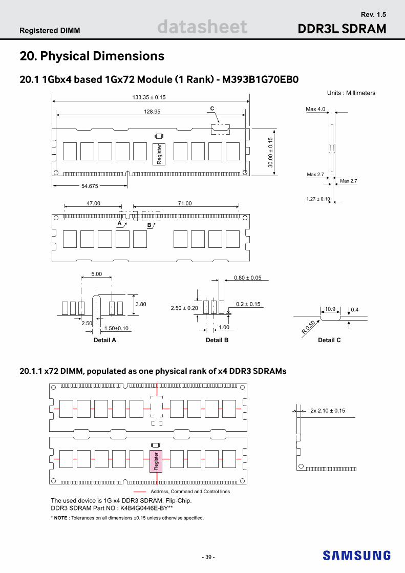
- 39 -
datasheet DDR3L SDRAMRev. 1.5
Registered DIMM
20. Physical Dimensions
20.1 1Gbx4 based 1Gx72 Module (1 Rank) - M393B1G70EB0
133.35 ± 0.15
A B
47.00 71.00
Units : Millimeters
128.95
1.00
0.2 ± 0.152.50 ± 0.20
Detail B
5.00
Detail A
1.50±0.10
0.80 ± 0.05
3.80
2.50
C
Detail C
10.9
R 0.50
0.4
30.0
0 ±
0.15
54.675
Reg
iste
r
1.27 ± 0.10
Max 2.7
Max 4.0
Max 2.7
20.1.1 x72 DIMM, populated as one physical rank of x4 DDR3 SDRAMs
The used device is 1G x4 DDR3 SDRAM, Flip-Chip.DDR3 SDRAM Part NO : K4B4G0446E-BY*** NOTE : Tolerances on all dimensions ±0.15 unless otherwise specified.
Address, Command and Control lines
Reg
iste
r
2x 2.10 ± 0.15

- 40 -
datasheet DDR3L SDRAMRev. 1.5
Registered DIMM
20.2 512Mbx8 based 1Gx72 Module (2 Ranks) - M393B1G73EB0
133.35 ± 0.15
A B
47.00 71.00
Units : Millimeters
128.95
1.00
0.2 ± 0.152.50 ± 0.20
Detail B
5.00
Detail A
1.50±0.10
0.80 ± 0.05
3.80
2.50
C
Detail C
10.9
R 0.50
0.4
30.0
0 ±
0.15
54.675
Reg
iste
r
1.27 ± 0.10
Max 2.7
Max 4.0
Max 2.7
20.2.1 x72 DIMM, populated as two physical ranks of x8 DDR3 SDRAMs
The used device is 512M x8 DDR3L SDRAM, Flip-Chip.DDR3L SDRAM Part NO : K4B4G0846E-BY*** NOTE : Tolerances on all dimensions ±0.15 unless otherwise specified.
Address, Command and Control lines
Reg
iste
r
2x 2.10 ± 0.15

- 41 -
datasheet DDR3L SDRAMRev. 1.5
Registered DIMM
20.3 1Gbx4 based 2Gx72 Module (2 Ranks) - M393B2G70EB0
Units : Millimeters
128.95
Detail B
Reg
iste
r
C
Detail C
10.9 0.4
B
133.35
30.0
0
71.00
54.675
47.00
Detail A
A
5.00
1.50±0.10
3.80
2.50 1.00
0.2 ± 0.152.50 ± 0.20
0.80 ± 0.05
1.27 ± 0.10
Max 2.7
Max 4.0
Max 2.7
20.3.1 x72 DIMM, populated as two physical ranks of x4 DDR3 SDRAMs
The used device is 1G x4 DDR3L SDRAM, Flip-Chip.DDR3L SDRAM Part NO : K4B4G0446E-BY*** NOTE : Tolerances on all dimensions ±0.15 unless otherwise specified.
Address, Command and Control lines
Regi
ster
2x 2.10 ± 0.15

![4Gb E-die DDR3L SDRAM Only x16...- 5 - K4B4G1646E datasheet DDR3L SDRAM Rev. 1.1 1. Ordering Information [ Table 1 ] Samsung 4Gb DDR3L E-die ordering information table NOTE: 1. Speed](https://img.pdfslide.us/doc/110x75/5e61d9961906103bcb7627ba/4gb-e-die-ddr3l-sdram-only-x16-5-k4b4g1646e-datasheet-ddr3l-sdram-rev-11.jpg)