Embed Size (px)
Citation preview

DesignCon 2004
Channel Compliance Testing Utilizing Novel Statistical Eye Methodology
Anthony Sanders, Infineon Technologies Tel: +49 170 6344266 Email: [email protected]
Mike Resso, Agilent Technologies Tel: 707.577.6529 Email: [email protected] John D’Ambrosia, Tyco Electronics Tel: 717.986.5692 Email: [email protected]

Abstract New growth demands in the bandwidth requirements for short and long reach electrical channels have pushed the performance limitations of traditional linear passive interconnects such as high-speed backplanes and connectors. Most chip and system vendors regard 3Gbps data rates over copper as mature technology today and are rapidly prototyping 6Gbps and 10Gbps hardware. Original standardisation work for high-speed digital interfaces focused on defining the transmitter and receiver compliance in terms of eye diagram analysis utilizing masks and jitter tolerance. The remaining work of defining complete channel requirements is less accurately defined. As the bandwidth and crosstalk limits of the electrical interface are approached, the ultimate result is a degradation of bit error rate over the physical layer. This undesirable effect mandates the need to fully characterise the capability of the electrical channel from end-to-end. Traditional methods to simulate an emphasised transmitter, physical channel, and equalising receiver in the time domain or frequency domain are not sufficient. Low probability events can not be accurately modelled without long simulation times. To optimise the efficiency of simulations, a novel methodology based on statistical methods is introduced that allows fast and accurate compliance testing of differential channels. The following paper describes the algorithm and compares measurement results to a Matlab implementation of the algorithm using a design case study of 3Gbps and 6Gbps transmitter technology in 0.13um CMOS.
Authors Biographies Anthony Fraser Sanders received his BEng degree with Honours in Electrical and Electronic Engineering from the University of Nottingham, England in 1991. Anthony joined Infineon Technology, formerly Siemens HL, in 1996 and as Principal Engineer is responsible for Analog Concept Engineering within Infineon's Optical Networking Group, developing Bipolar & CMOS 3/6/10/40Gbit Line Card products. His current research activities focus on the theoretical understanding of Jitter phenomena based on observation from laboratory measurement, the modelling and optimization of optical & electrical serial links using equalization and on the limits of CMOS technology in it's application to high speed serial interfaces. Anthony has chaired the IEEE adhoc on XAUI jitter, various OIF jitter adhocs and is currently one of the editors of OIF’s Common Electrical I/O (CEI) standard and author of the “StatEye”.
Mike Resso is a Product Manager in the Signal Integrity Operation of Agilent Technologies. He is responsible for technical training of Agilent field engineers and interfacing with Agilent R&D engineers to bring innovative products to market. Mike has over twenty years of experience in the test and measurement industry and has focused on understanding signal integrity issues from both time domain and frequency domain perspectives. His most recent activity is developing applications techniques for complete 4-port characterization utilizing Time Domain Reflectometry (TDR) and Vector Network Analysis (VNA). Mike has previous experience in the design and development of electro-optic test instrumentation and has published numerous technical papers. Mike received his Bachelor of Science degree in Electrical and Computer Engineering from University of California.
John D'Ambrosia is the Manager of Semiconductor Relations for Tyco Electronics in Harrisburg, PA. John works with semiconductor vendors to explore the interaction between semiconductor devices and Tyco Electronics interconnect solutions. This has led to his involvement in standards bodies defining solutions for backplane environments. He was an active participant in the development of XAUI, and served as the chair of the 10 Gigabit Ethernet Alliance XAUI Interoperability Group, which drove interoperability testing for XAUI solutions for the industry. He helped organize the High Speed Backplane Initiative (HSBI), as well as served as its secretary. Currently, John is serving as the chair of the Optical Internetworking Forum's (OIF) Market Awareness & Education Committee, and is participating in the development of the OIF Common Electrical I/O (CEI) project. John received a B.S. in Electrical Engineering Technology from the Pennsylvania State University in 1989 and a Master's Degree in Engineering Management from the National Technology University in 1999.
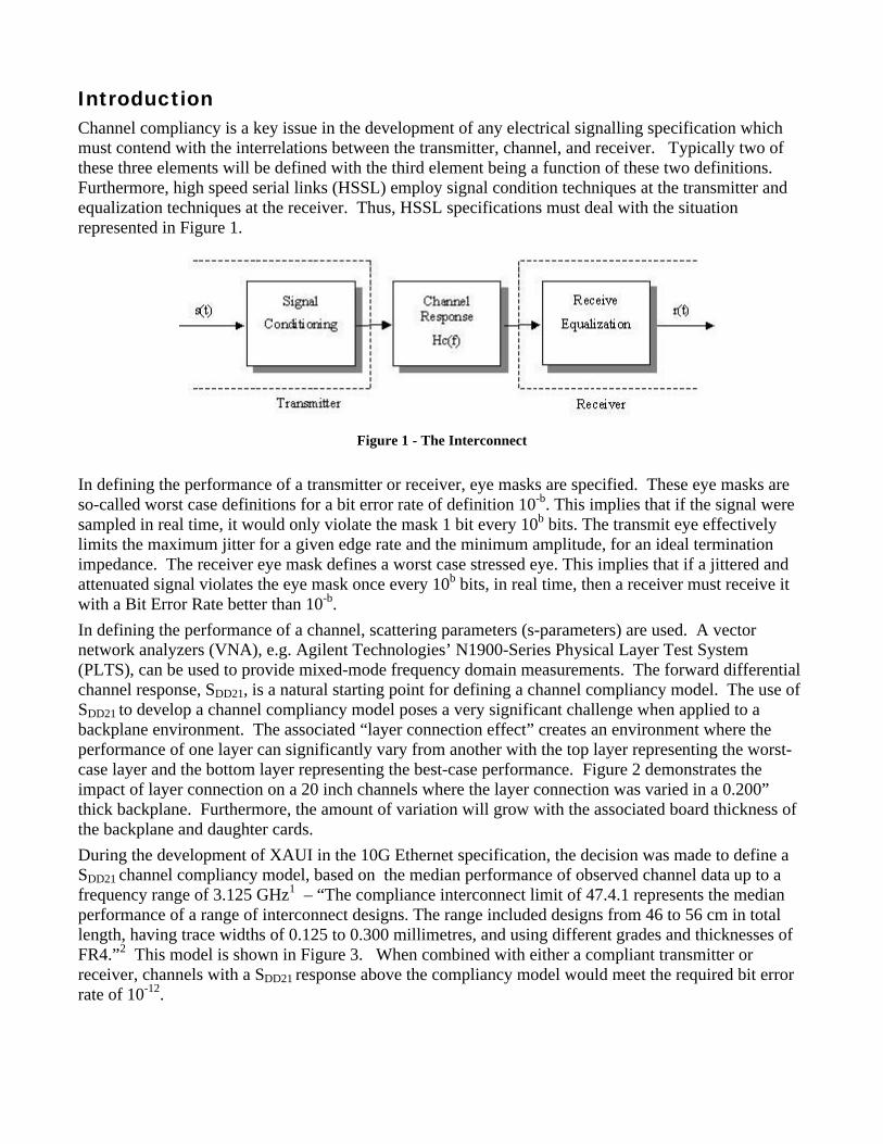
Introduction Channel compliancy is a key issue in the development of any electrical signalling specification which must contend with the interrelations between the transmitter, channel, and receiver. Typically two of these three elements will be defined with the third element being a function of these two definitions. Furthermore, high speed serial links (HSSL) employ signal condition techniques at the transmitter and equalization techniques at the receiver. Thus, HSSL specifications must deal with the situation represented in Figure 1.
Figure 1 - The Interconnect
In defining the performance of a transmitter or receiver, eye masks are specified. These eye masks are so-called worst case definitions for a bit error rate of definition 10-b. This implies that if the signal were sampled in real time, it would only violate the mask 1 bit every 10b bits. The transmit eye effectively limits the maximum jitter for a given edge rate and the minimum amplitude, for an ideal termination impedance. The receiver eye mask defines a worst case stressed eye. This implies that if a jittered and attenuated signal violates the eye mask once every 10b bits, in real time, then a receiver must receive it with a Bit Error Rate better than 10-b. In defining the performance of a channel, scattering parameters (s-parameters) are used. A vector network analyzers (VNA), e.g. Agilent Technologies’ N1900-Series Physical Layer Test System (PLTS), can be used to provide mixed-mode frequency domain measurements. The forward differential channel response, SDD21, is a natural starting point for defining a channel compliancy model. The use of SDD21 to develop a channel compliancy model poses a very significant challenge when applied to a backplane environment. The associated “layer connection effect” creates an environment where the performance of one layer can significantly vary from another with the top layer representing the worst-case layer and the bottom layer representing the best-case performance. Figure 2 demonstrates the impact of layer connection on a 20 inch channels where the layer connection was varied in a 0.200” thick backplane. Furthermore, the amount of variation will grow with the associated board thickness of the backplane and daughter cards. During the development of XAUI in the 10G Ethernet specification, the decision was made to define a SDD21 channel compliancy model, based on the median performance of observed channel data up to a frequency range of 3.125 GHz1 – “The compliance interconnect limit of 47.4.1 represents the median performance of a range of interconnect designs. The range included designs from 46 to 56 cm in total length, having trace widths of 0.125 to 0.300 millimetres, and using different grades and thicknesses of FR4.”2 This model is shown in Figure 3. When combined with either a compliant transmitter or receiver, channels with a SDD21 response above the compliancy model would meet the required bit error rate of 10-12.

Figure 2 - Impact of Layer Connection
Figure 3 – XAUI Channel Model
Looking at the channel response in the frequency domain is fundamental to gaining insight into the performance of the channel and how it affects the signal feeding into the receiver using either Fourier transforms ( )( ) ( ) fHtsfftiffttr ⋅= or standard time domain simulators capable of accepting the s-parameters. The XAUI channel model, however, is truly only informative, as the impact of discontinuities and group delay are not represented. It is smooth in comparison to the real channels shown in Figure 2, with no apparent ripple. These ripples can easily result in a “dipping” below the channel compliancy model at various frequencies. This leads to concern regarding whether the channel will operate as intended since the channel compliancy model has not been met. So from a specification perspective the limitations of this type of channel compliancy model make it more useful for informative purposes than normative purposes. Thus as equalization schemes such as transmit emphasis and receiver equalization are introduced to push a given channel’s bit error rate to its theoretical limit a new channel compliancy methodology is needed by the user. This methodology needs to look at the channel as part of the system, illustrated in Figure 1, rather than on its own merits. This methodology needs to utilize all the information provided by 4 port s-parameter characterization combination with the total jitter present at the receiver sampler to give insight into the bit error rate performance of the total system.

Total sampling jitter is contributed from the transmitter, channel and receiver. However the jitter introduced by the channel is inherently contained within the s-parameters and, as will be explained, is a function of the transmitter. Jitter is best defined by understanding the bathtub representation i.e. the measurement bit error rate or inverse error function (Q) versus the sampling offset. Gaussian Jitter (GJ), otherwise known as Random Jitter, is defined as the gradient of the linearised portion of the bathtub at the bit error rate of interest. High Probability Jitter (HPJ), otherwise known as Deterministic Jitter, is the intersection of the linearization at the x-axis where Q=0. This model, shown in Figure 4, is formally known as a Dual Dirac model and allows the system designer to add all HPJ terms in the link linearly, and to Root Mean Square all GJ terms. The GJ terms are then multiplied by the twice the Q required by the link to give the Total GJ. And the Total Jitter calculated as the linear sum if the Total HPJ and Total GJ, which must be then less than 1Unit Interval for the link to work.
Figure 4 – Dual Dirac Model
It is necessary to fully characterize the interconnect capability from the transmitter through the channel to the receiver. It is also necessary to employ a statistical methodology that will capture the impact of low probability events. The S-parameter characterization of the channel and system will provide the building blocks for further simulation and analysis that will provide the quantitative answers. This will allow the inclusion of:
• real channel data, including phase data and mode conversions • in-band crosstalk resulting from similar switching signals • out-of-band or alien crosstalk resulting from other signalling • transmit jitter • receiver jitter
The inclusion of all of these parameters can then be applied statistically to the problem at hand to determine the channel’s expected bit error rate in the system and its compliancy to the targeted specification. Infineon Technologies has developed such a technique referred to as “StatEye.” The focus of this paper will be to explain this technique utilizing backplane channels from Tyco Electronics HM-Zd Legacy Backplane. Validation testing of the technique will be provided by Agilent Technologies.
StatEye Methodology Pulse Response Theory The pulse response of a channel can be understood as the signal resulting when an NRZ pulse, ( )ttx , is transmitted through the channel under investigation. The NRZ pulse has a width equal to the period of the bit rate of interest and therefore the pulse response is only valid for a specific baud rate.Given that the transfer function of the channel, ( )ωS , is known in the frequency domain, the pulse response is best calculated by multiplying it with the fast Fourier transform of the NRZ pulse, ( )ωtx .
( ) ( ) ( )( ) ( )( )( ) ( ) ( )( ) ( )( )ω=
ω⋅ω=ω=ω
−⋅=
rxiFFTtrxStxrx
ttxFFTtx
ttHtHttx period
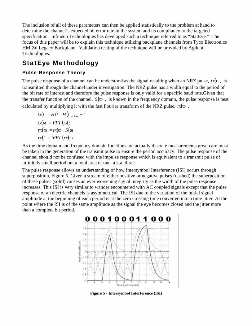
As the time domain and frequency domain functions are actually discrete measurements great care must be taken in the generation of the transmit pulse to ensure the period accuracy. The pulse response of the channel should not be confused with the impulse response which is equivalent to a transmit pulse of infinitely small period but a total area of one, a.k.a. dirac. The pulse response allows an understanding of how Intersymbol Interference (ISI) occurs through superposition, Figure 5. Given a stream of either positive or negative pulses (dashed) the superposition of these pulses (solid) causes an ever worsening signal integrity as the width of the pulse response increases. This ISI is very similar to wander encountered with AC coupled signals except that the pulse response of an electric channels is asymmetrical. The ISI due to the variation of the initial signal amplitude at the beginning of each period is at the zero crossing time converted into a time jitter. At the point where the ISI is of the same amplitude as the signal the eye becomes closed and the jitter more than a complete bit period.
Figure 5 - Intersymbol Interference (ISI)

Equalisation Bandwidth limitations can be equalised by cascading the channel with a linear time continuous filter, i.e. one that can be represented in both the time and frequency domain, which is the exact inverse pulse response of the channel. Given this theoretical filter response the resulting transfer function would be a linear response with constant gain over frequency. As this type of filter is both theoretical and impractical to build an approximation is usually used. Working at lower bit rates, where accurate signal processing can be performed, a resulting raised cosine spectrum or partial response can be achieved3. For higher bit rates where only simple equalisation can be implemented the time continuous filter is usually only a finite number of zeros and poles. By optimal placement of these zeros and poles an enhancement of the bandwidth of the channel can be achieved which to a certain degree approaches a simplified partial response. A simple example, Figure 6, shows how the frequency response of the channel is increased in bandwidth and the resulting pulse response is narrowed, which results in a reduction of ISI.
Figure 6 - Equalised Frequency and Pulse Response
The disadvantage of linear time continuous equalisers can be understood by considering the crosstalk frequency response. The crosstalk frequency response is the transfer function of a Near End Crosstalk Aggressor Tx pair (NEXT) or Far End Crosstalk Aggressor Tx pair (FEXT) to the receiver, Figure 7. The equaliser described above for example, will enhance this crosstalk frequency response in the same way, increasing the crosstalk energy at the receiver thus decrease the resulting total received signal.
Figure 7 - Crosstalk Definitions
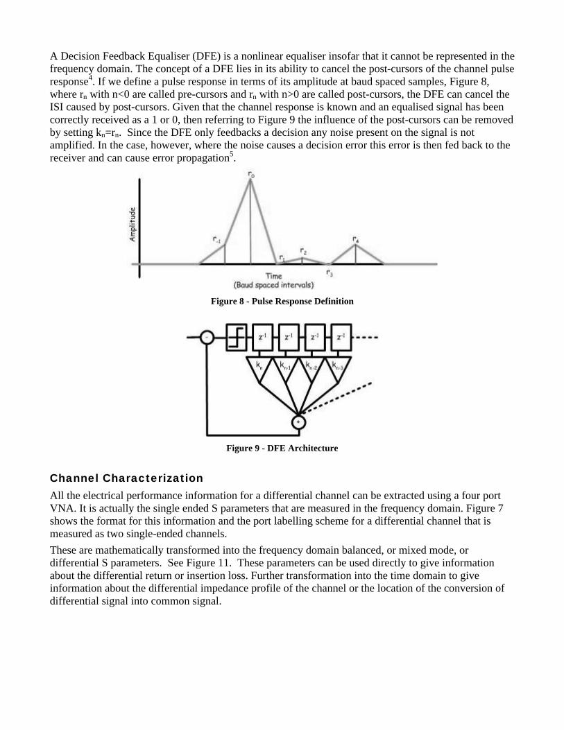
A Decision Feedback Equaliser (DFE) is a nonlinear equaliser insofar that it cannot be represented in the frequency domain. The concept of a DFE lies in its ability to cancel the post-cursors of the channel pulse response4. If we define a pulse response in terms of its amplitude at baud spaced samples, Figure 8, where rn with n<0 are called pre-cursors and rn with n>0 are called post-cursors, the DFE can cancel the ISI caused by post-cursors. Given that the channel response is known and an equalised signal has been correctly received as a 1 or 0, then referring to Figure 9 the influence of the post-cursors can be removed by setting kn=rn. Since the DFE only feedbacks a decision any noise present on the signal is not amplified. In the case, however, where the noise causes a decision error this error is then fed back to the receiver and can cause error propagation5.
Figure 8 - Pulse Response Definition
Figure 9 - DFE Architecture
Channel Characterization All the electrical performance information for a differential channel can be extracted using a four port VNA. It is actually the single ended S parameters that are measured in the frequency domain. Figure 7 shows the format for this information and the port labelling scheme for a differential channel that is measured as two single-ended channels. These are mathematically transformed into the frequency domain balanced, or mixed mode, or differential S parameters. See Figure 11. These parameters can be used directly to give information about the differential return or insertion loss. Further transformation into the time domain to give information about the differential impedance profile of the channel or the location of the conversion of differential signal into common signal.

Figure 10 - Lab Setup
Figure 11 - S Parameters Quadrants
In order to interpret the large amount of data in the differential parameter matrix, it is helpful to analyze one quadrant at a time. The first quadrant is defined as the upper left 4 parameters describing the differential stimulus and differential response characteristics of the device under test. This is the actual mode of operation for most high-speed differential interconnects, so it is typically the most useful quadrant that is analyzed first. It includes input differential return loss (SDD11), input differential insertion loss (SDD21), output differential return loss (SDD22) and output differential insertion loss (SDD12). Note the format of the parameter notation SXYab, where “S” stands for Scatttering Parameter or S-Parameter, “X” is the response mode (differential or common), “Y” is the stimulus mode (differential or common), “a” is the output port and b is the input port. This is typical nomenclature for frequency domain scattering parameters. All sixteen differential S-Parameters can be transformed into the time domain by performing an Inverse Fast Fourier Transform (IFFT). The matrix representing the time domain will have similar notation, except the “S” will be replaced by a “T” (i.e. TDD11). The second and third quadrants are the upper right and lower left 4 parameters, respectively. These are also referred to as the mixed mode quadrants. This is because they fully characterize any mode conversion occurring in the device under test, whether it is common-to-differential conversion (EMI susceptibility) or differential-to-common conversion (EMI radiation). Understanding the magnitude and

location of mode conversion is very helpful when trying to optimize the design of interconnects for gigabit data throughput. The fourth quadrant is the lower right 4 parameters and describes the performance characteristics of the common signal propagating through the device under test. For a properly designed device there should be minimal mode conversion and the fourth quadrant data is of little concern. However if any mode conversion is present due to design flaws then the fourth quadrant will describe how this common signal behaves.
Cascading of Channel with Transmitter and Receiver Return Loss Model After the full s-parameters of a channel have been measured the effect of reflections can be modelled using a worst case transmitter and receiver return loss. After converting the s-parameters into the transmission matrix6, performing a matrix multiplication and converting back to the s-parameters, the overall transfer function is obtained. Given:
nmS is the measured 4 port differential data of the channel
Tx is the transmitter return loss Tx is a single pole filter Rx is the receiver return loss
( )ωTr is the channel response transfer function as defined
( ) ( )( )
( ) ( )( ) ( )
( )
ω⊗
ωωωω
⊗
ωω
=ωRx
SSSS
TxTx
Tr
In addition to the return loss, a typical transmitter is not capable of generating an ideal NRZ pulse so the transfer function is additionally multiplied by a single pole filter with a corner frequency of 0.75xfbaud, typical for CML style outputs.
Theoretical Analysis of Receiver Pulse Response The superposition of post-cursors and pre-cursors to form ISI is statistical in nature. Given a full random binary data stream and a finite number of cursors, each possible combination of cursors can superimpose each with equal probability. A simple example, Figure 12, with an arbitrary sample time has one pre-cursor and two post-cursors and shows how the eight possible combinations of the cursors can combine to cause ISI. In this example the ISI is as large as the signal itself and closes the eye. The probability of each amplitude can be represented by a Conditional Probability Distribution Function which for this example is simply eight diracs or deltas, δ , of equal probability i.e. 1/8. As more cursors are taken into account the number of possible combination increases and the Probability Distribution becomes more detailed and can be represented mathematically taking into account the effect of the DFE cancellation of the post-cursors.

Figure 12 - ISI PDF
Given, ( )τnr are the cursors of the pulse response at sampling time τ
be is the ideal static equalisation coefficients of the b tap DFE ( )τc is the set of equalised cursors at sampling time τ
( ) −
→= ε
εετδ x is the dirac or delta function
( ) ( ) ( ) ( ) ( ) ( ) ( )
[ ]( )
( ) ( ) ( )( )∑
∑
=
−
=
−
+−−
−−⋅=
=
+
⋅=
=
−−=
mnnm
m
b
mb
bn
mn
mnnnnn
mbbbm
ISIdcISIp
n
dn
dddddd
rrererrrc
τδτ
τττττττ
where, nd are the possible combinations of the data stream and is either 1 or 0 ( )τISIp is the probability of a given ISI occurring
It would seem from the methodology that to calculate the PDF of a pulse response with a large number of cursors, >10, all possible combination would have to be calculated e.g. for 30 cursors 230 combinations would have to be calculated. This sledge hammer approach is not necessary as the problem can be broken down into small problems.

Given, c is an example set of four cursors
nd are the possible combination of bits in the data stream
[ ][ ]
( )
( ) ( )( )
( )( ) ( )( )
−−⋅∗
−−⋅≡
−−⋅=
=
+
⋅=
=
=
∑∑
∑
∑
==
=
−
=
nn
nn
nn
b
b
bn
nnnnn
ISIdcISIdc
ISIdcISIp
n
dn
ddddd
ccccc
δδ
δ
Given an example of four cursors, the PDF can either be calculated from 24 diracs or the convolution of two PDFs calculated from 22 diracs. In this way a pulse response of 40 cursors could be calculated by convoluting 20 smaller PDF calculated from 22 diracs. The saving in required processing steps can clearly be seen.
Figure 13 - Family of Conditional PDFs
For each arbitrary sample point within the pulse response a Conditional PDF can be calculated, forming a family of Conditional PDFs, Figure 13. Due to the discretisation when storing and building a PDF an accuracy error occurs that can be defined, Figure 14. Given that the discrete PDF array is defined from –AMAX to AMAX and has m bins, then the error of a single entry has a defined bin error, ε

Figure 14 - Binning of PDF
where m
AMAXm
AMAX>>− ε
For each convolution the error accumulates and can be represented for the simple example above
( )( ) ( )( )
( ) ( )[ ]( ) ( )[ ]
( )[ ]εεδ
εδεδ
εδεδ
δδ
++⋅+⋅+⋅+⋅=
−+⋅+⋅−+⋅+⋅
∗−+⋅+⋅−+⋅+⋅=
−−⋅∗
−−⋅=
=
∑∑=
+=
dcdcdcdc
ISIdcdcISIdcdc
ISIdcdcISIdcdc
ISIdcISIdc
ISIpISIpISIp
nnn
nnn
cccccc
Given that the bin error associated with a PDF is evenly distributed with a zero mean and
variance nεσµ == then N convoluted PDFs will also have a bin error with zero mean but a variance
of nN εσµ == . The peak error given a probability equal to the Bit Error Rate of interest is then
σ⋅Q where Q is the inverse error function of the probability of interest. E.g.
≈≈⋅=
⋅≈⋅=
====
−==
−
µε
µ
ε
BERN
NmAMAX
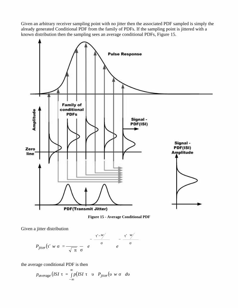
Given an arbitrary receiver sampling point with no jitter then the associated PDF sampled is simply the already generated Conditional PDF from the family of PDFs. If the sampling point is jittered with a known distribution then the sampling sees an average conditional PDFs, Figure 15.
Figure 15 - Average Conditional PDF
Given a jitter distribution
( )
+⋅σ
⋅π
=στ′
σ
+τ′−
σ
−τ′−
ww
jtter eewP
the average conditional PDF is then
( ) ( )∫ ( ) υ⋅συ⋅υ+τ=τ∞
∞−dwPISIpISIp jtteraverage
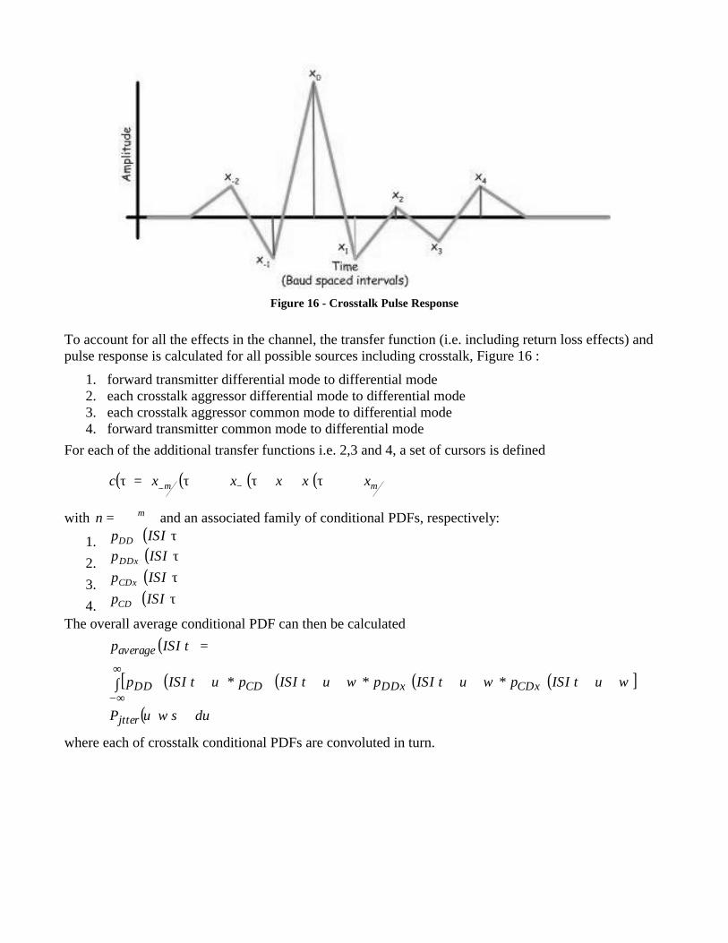
Figure 16 - Crosstalk Pulse Response
To account for all the effects in the channel, the transfer function (i.e. including return loss effects) and pulse response is calculated for all possible sources including crosstalk, Figure 16 :
1. forward transmitter differential mode to differential mode 2. each crosstalk aggressor differential mode to differential mode 3. each crosstalk aggressor common mode to differential mode 4. forward transmitter common mode to differential mode
For each of the additional transfer functions i.e. 2,3 and 4, a set of cursors is defined
( ) ( ) ( ) ( )
τττ=τ −− mm xxxxxc
with += mn and an associated family of conditional PDFs, respectively:
1. ( )τISIpDD 2. ( )τISIpDDx 3. ( )τISIpCDx 4. ( )τISIpCD
The overall average conditional PDF can then be calculated
( )
( ) ( ) ( ) ( )[ ]∫
( ) υσυ
υτυτυτυτ
τ
dwP
wISIpwISIpwISIpISIp
ISIp
jtter
CDxDDxCDDD
average
⋅
⋅++∗++∗++∗+
=
∞
∞−
where each of crosstalk conditional PDFs are convoluted in turn.

The arbitrary position of ( )τISIpaverage can now be swept over the complete pulse to give a family of average conditional PDFs, Figure 17a/b. Using a contour algorithm the points of equal probability of the integrated PDFs can be drawn creating a “so-called” StatEye, Figure 17c. This StatEye shows the probability of receiving a specific amplitude for a given arbitrary receiver sampling point.
Figure 17 - StatEye Contouring
By plotting the probability at the zero amplitude crossing for the family of CDF against the receiver sampling point, a Bathtub, Figure 17d is generated from which the Gaussian and High Probability Jitter can be extracted.

Implementation The implementation of such an algorithm is feasible on a typical >1GHz processor within interpreting languages such as Matlab®. Matlab provides a user friendly and fast prototyping interfaces that allows the algorithm to be implemented and debugged.
Figure 18 - Implementation Execution and Data Flow
A recommended flow, shown in Figure 18, consists of three non-nested loops. Loop#1 scans the pulse response, initially storing the cursor values. Loop#2 then calculates the Conditional PDFs and loop#3 scans the pulse again and calculates the Average Conditional PDFs. Using time set intervals of 0.01Unit Intervals and typically 1000 bins for the PDFs a good compromise between accuracy and execution time (~30 seconds) is found. If faster execution times are necessary then it is recommended to move to a C implementation where execution times can be increased by a factor of four. However it is recommended that this step only be taken after an initial implementation in Matlab. A version of this algorithm is currently under development which will interface directly to Agilent’s PLTS software.

System Budgeting and Interoperability Using the “StatEye” methodology systems can be budgeted which incorporate both transmit and receiver equalisation and utilise adaptive algorithms. To ensure interoperability the transmitter is controlled by defining an eye mask which limits the Gaussian and High Probability Jitter and ensures a certain signal amplitude. Defining the channel as the combined forward response and “all” significant crosstalk responses, the cascaded channel with a representative transmitter and receiver return loss is defined as being compliant if the resultant “StatEye” for a worst case transmit signal and an ideal receiver DFE filter meets a worst case eye mask i.e. it has an amplitude and a GJ and HPJ better than that defined. The receiver should be capable of receiving a worst case stressed7 eye with a bit error rate better than that required of the system. Given that the “StatEye” analysis is performed with an ideal DFE and no receiver sampling jitter this allows a standard to not impose any ideas or assumptions concerning the penalties associated with the implementation. A designer of such a receiver should through simulation
• estimate the sampling jitter and add this to the transmitter jitter • estimate the DFE penalties and adjust the cursor set • recalculate the “StatEye” using the total sampling jitter is then verify that the reciever’s
sampler is capable of receiving it. The “StatEye” therefore uses the Dual Dirac model only as a means of quantifying the jitter present at certain points in the system without relying upon the invalid Dual Dirac “addition” of GJ and HPJ over a bandlimited channel. Because the “StatEye” is not defining an exact implementation of the channel but merely and overall performance of the channel, it allows the PCB implementer to trade-off certain parameters against each other e.g. channel length can be decreased, in turn decreasing attenuation, allowing crosstalk to increase.
Design Example Results Channel Description Tyco Electronics announced the availability of its HM-Zd Legacy Interoperability Platform in August of 2003. This platform provides the industry with a backplane that is representative of the conditions seen in typical system vendor environments. The “Legacy” Platform builds upon Tyco Electronics HM-Zd XAUI Interoperability Platform, which the 10Gigabit Ethernet Consortium selected as a common platform for interoperability testing in early 2001. The HM-Zd Legacy Backplane platform is conceptually shown in Figure 19. It consists of 2 line cards that provide SMA access and the Z-PACK HM-Zd based backplane. Each line card is 0.093” (nominal) thick, consists of 14 layers, and is fabricated using Nelco 4000-2 material. There are four signal layers distributed throughout the entire stackup where the 100Ω differential geometries are based on 0.006” (nominal) wide traces. The trace length from the SMA to the Z-PACK HM-Zd connector is two inches. The backplane is 0.200” (nominal) thick, consists of 18 layers, and is fabricated using 4000-6 material. There are six signal layers distributed throughout the entire stackup where the 100Ω differential geometries are based on 0.0055” (nominal) wide traces. On the backplane there are three sets of trace lengths – 1”, 16”, and 30”. Thus, for the platform there are overall system lengths of 5”, 20”, and 34”.
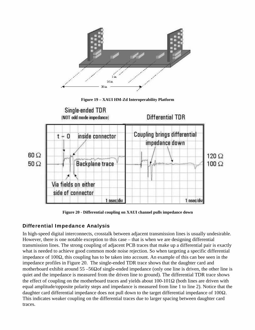
Figure 19 – XAUI HM-Zd Interoperability Platform
Figure 20 - Differential coupling on XAUI channel pulls impedance down
Differential Impedance Analysis In high-speed digital interconnects, crosstalk between adjacent transmission lines is usually undesirable. However, there is one notable exception to this case – that is when we are designing differential transmission lines. The strong coupling of adjacent PCB traces that make up a differential pair is exactly what is needed to achieve good common mode noise rejection. So when targeting a specific differential impedance of 100Ω, this coupling has to be taken into account. An example of this can bee seen in the impedance profiles in Figure 20. The single-ended TDR trace shows that the daughter card and motherboard exhibit around 55 –56Ωof single-ended impedance (only one line is driven, the other line is quiet and the impedance is measured from the driven line to ground). The differential TDR trace shows the effect of coupling on the motherboard traces and yields about 100-101Ω (both lines are driven with equal amplitude/opposite polarity steps and impedance is measured from line 1 to line 2). Notice that the daughter card differential impedance does not pull down to the target differential impedance of 100Ω. This indicates weaker coupling on the differential traces due to larger spacing between daughter card traces.

Mode Conversion Analysis When a differential signal is propagating through an ideal differential transmission line, there theoretically should be no other mode transmitting. If there is anything that is different on one line of the differential channel from the other line of the differential channel, then we have something called mode conversion. This will result in EMI problems, the severity of which depends upon the type of mode conversion and application. Mode conversion relating to high speed digital channels can be grouped into two categories: mode conversion caused by active devices and mode conversion caused by passive devices. An example of active device mode conversion would be if a differential transmitter or amplifier had one drive signal different from the other supposedly complementary drive signal, either voltage, current or skew. An example of a passive device mode conversion would be if a differential connector had different characteristic impedance lines, different length pins, or different loading on each line such as ground plane discontinuities. In any case, mixed mode analysis can be a powerful tool in locating obstacles that limit the highest possible data rate transmission in interconnects. As seen in Figure 21, the differential-to-common mode conversion can be quantified as a percentage of amplitude by overlaying the forward time domain transmission waveform (TDD21) with the forward time domain transmission mode conversion waveform (TCD21). As expected, TDD21 shows the propagation delay and rise time transition of the degraded signal at the output of the device under test. The resulting measurement is the mode conversion waveform showing 7% of the original signal.
Figure 21 - Measuring forward time domain transmission (TDD21) and superimposing differential-to-common
transmission mode conversiuon yields an indication of EMI radiation

CMOS 0.13um Design Case A typical 0.13um pure CMOS design is capable of implementing a multiple transceiver channels on one piece of silicon. This typically can lead to problems of crosstalk which limit the maximum performance achievable. For the purpose of comparison two links shall be analysed:
1. a 3.125Gbps XAUI transceiver with emphasised transmitter and traditional receiver 2. a 6.25Gbps transceiver with 5 tap DFE receiver
For the purpose of analysis of the channel the electrical characteristics defined in Table 1 shall be assumed
Table 1 – Assumed Electrical Characteristics
StatEye Analysis The return loss model of the transmitter, Figure 22, and receiver is a smooth response defined by a simple parallel resistor with 60Ω and a capacitor such that the return is just violating the specification at ¾ the baud rate. The return loss of the channel returns a large amount of energy that increases the reflections and resonances of the forward transfer function. The pulse response of the forward channel, Figure 23, can be seen to contain post cursors out to 53UI (+7UI) for 6.25Gbps compared to the 3.125Gbps, highlighting the need for additional receiver equalisation. The influence of reflections at 6.25Gbps can be seen in the tail at 56UI which are enhanced due to the non-ideal return loss of the transmitter and receiver.

Figure 22 - Sdd21 with Return Loss of 6.25Gbps Link
Figure 23 - Pulse Response for 3.125 Gbps and 6.25 Gbps NRZ Transmit Pulse
Although no crosstalk measurements were available two crosstalk models were generated from the SDD11, Figure 24, to show the influence of return loss, transmit emphasis and DFE. The crossover of the return loss and forward channel for the -30dB crosstalk example is already at ¾ the baud rate for 6.25Gbps demonstrating that a simple analog bandwidth enhancement filter would additionally boost the crosstalk.

Figure 24 - -30dB & -40dB Generated Crosstalk Transfer function
After allowing the “StatEye” script to optimise the transmit emphasis coefficients8, the resulting eye and bathtub, Figure 25, for the required Q, has an amplitude of 88mVsepp (0.22 normalised to the transmit amplitude) with a Gaussian Jitter of 0.014UIrms and High Probability Jitter of 0.265UIpp. When using the total sampling jitter for the calculation of the “StatEye”, Figure 26, the effect of the receiver jitter can be seen to decrease the amplitude of the signal to 52mV (0.13) and increase the jitter to 0.020UIrms and 0. 397UIpp. It can be seen that the additional receiver jitter does not add classically using dual dirac theory again, clearly demonstrating the need for the “StatEye” methodology.
Figure 25 - 3.125Gbps StatEye & Bathtub with only Transmit Jitter

Figure 26 - 3.125Gbps StatEye & Bathtub with Total Sampling Jitter
As the baud rate is increased to 6.25Gbps the increased width of the pulse response causes the “StatEye” without additional equalisation to close. Using again an optimisation script for find the coefficients of the DFE the “StatEye” is calculated for the Total Sampling Jitter and -40dB crosstalk. The resultant eye, Figure 27, for the required Q, has an amplitude of 50mV (0.125)with 0.022UIrms and 0.196UIpp jitter, which corresponds to the requirements of the sampler. It should be noted that the worst case “StatEye” does not represent a single worst case signal as this would correspond to a bit period of 49ps. As the crosstalk is increase to -30dB a loss in eye opening is incurred, Figure 28, however unlike a time continuous filter the loss of amplitude is linear and not emphasised and would still allow a workable system.
Figure 27 - 6.25Gbps StatEye & Bathtub with Transmit Jitter and -40dB Crosstalk

Figure 28 - 6.25Gbps StatEye & Bathtub with Transmitter Jitter and -30dB Crosstalk
Conclusion In this paper we have outlined the “Legacy” Methodology used by XAUI and explained under what conditions limitations become unacceptable as the channel is pushed to its limit either in terms of speed or bit error rate. The “StatEye” methodology was then introduced, explaining how the statistical methodology in combination with the use of the full s-parameter information of the forward channel and crosstalk aggressors enables the limitations to be overcome. A small explanation of the way in which the “StatEye” fits into the entire Standards and Interoperability picture showed how no additional requirements of the engineer is required in terms of hardware and also the problems of measuring “closed” eyes are circumvented. Finally an example of how a typical legacy channel can be measured with available equipment was demonstrated, pointing out typical problems using the frequency and time domain representation and ending with the “StatEye” results showing that for 6.25Gbps operation such a channel, given the appropriate circuitry, would be sufficient for bit error operation well below a bit error rate of 10-15. The “StatEye” methodology appears initially to be quite complex however in comparison to any typical simulation tool it is quite straight forward, demonstrated by its simple implementation in Matlab. Alternative methods using time or frequency domain analysis would seem to be able to give a similar result but care must be taken as the very low probability events are not possible to represent due to the
very long simulation times required e.g. −⋅ bits for a bit error rate of −⋅ . 1 The channel model is defined by the following equation: ( ) ( )[ ]fafafaefS ++−≤ where f is
frequency in Hz, −−− ⋅=⋅=⋅= aaa . 2 “IEEE802.3 2000”, IEEE, Clause 47.3.5, 2000 3 J.G.Proakis, M.Salehi, “Communication Systems Engineering”, Prentice-Hall, pp555, 1994 4 J.G.Proakis, M.Salehi, “Communication Systems Engineering”, Prentice-Hall, pp590, 1994 5 J.E.Smee, N.C.Beaulieu “Error-Rate Evaluation of Linear Equalization and Decision Feedback Equalization with Error
Propagation”, IEEE Trans. Commun, pp656, Vol.46, May 1998 6 Dr. Howard Johnson, “Scattering Parameters”, HIGH-SPEED DIGITAL DESIGN – online newsletter, Vol 6 Issue 03,
June 2003, http://signalintegrity.com/Pubs\news\6_03.htm 7 The generation and calibration of the stressed eye is not the subject of this paper. 8 The optimisation using a LMS gradient based algorithm, which is not the subject of this paper