Embed Size (px)
Citation preview

Application Note
CML MicrocircuitsCOMMUNICATION SEMICONDUCTORS
CMX649 Wireless Voice
Link Design Guide
AN/2WR/649Des/2 November 2004
CMX649 Wireless Voice Link Design Guide Page 1 of 42
1 Introduction The CMX649 is an innovative adaptive delta modulation (ADM) voice codec that was designed to serve in advanced wireless voice links. The purpose of this document is to present an example design that combines the CMX649 with other external components in a small form factor, low power, fully functional two-way wireless voice link.
This document presumes that the reader is familiar with the CMX649 and ADM voice coding. Additional background information can be obtained from the following application notes, which can be found at www.cmlmicro.com:
• “CMX649 Operation and Application”
• “CMX649 Recommended Settings”
• “Continuously Variable Slope Delta Modulation Tutorial”

CMX649 Wireless Voice Link Design Guide
© 2004 CML Microcircuits Page 2 of 42
TABLE OF CONTENTS 1 Introduction ......................................................................................................... 1 2 Targeted Application & Design Objectives .......................................................... 3 3 Description of Operation ..................................................................................... 3 4 Hardware Description.......................................................................................... 5
4.1 Voice Coding – CMX649.............................................................................. 5 4.2 RF Transceiver – MICRF505 ....................................................................... 7
4.2.1 Transmitter............................................................................................ 9 4.2.2 Receiver.............................................................................................. 11 4.2.3 Crystal Oscillator................................................................................. 12 4.2.4 Frequency Synthesizer ....................................................................... 12
4.3 Microcontroller – MSP430F1232................................................................ 13 4.3.1 Data Buffering Scheme....................................................................... 15
4.4 Battery ....................................................................................................... 18 4.5 Voltage Regulators .................................................................................... 19 4.6 Peripheral Functions .................................................................................. 19
5 Firmware Description ........................................................................................ 20 5.1.1 Interrupt Vectors ................................................................................. 21 5.1.2 RESET................................................................................................ 21 5.1.3 SETUP649.......................................................................................... 23 5.1.4 SETUPRF ........................................................................................... 23 5.1.5 MAINLOOP......................................................................................... 24 5.1.6 START_RFTX..................................................................................... 25 5.1.7 SET_RF_TX ....................................................................................... 25 5.1.8 RFCHIPTX.......................................................................................... 26 5.1.9 START_RFRX .................................................................................... 28 5.1.10 SET_RF_RX ....................................................................................... 30 5.1.11 RFCHIPRX ......................................................................................... 30 5.1.12 CMX649_TRANSFER......................................................................... 34
6 Circuit Schematics and Board Layout ............................................................... 36 7 Bill of Materials.................................................................................................. 40 8 Conclusion ........................................................................................................ 41

CMX649 Wireless Voice Link Design Guide
© 2004 CML Microcircuits Page 3 of 42
2 Targeted Application & Design Objectives The design presented in this document is targeted towards a low-power, small form-factor wireless headset product, but the information is readily adapted to other wireless voice applications. The objectives used to guide this design include:
• Small size consistent with mobile/cordless phone wireless headset form factor • Optimal sound quality • License-free operation • Low power consumption for maximum talk-time and standby-time • Lowest possible bill-of-materials (BOM) cost
3 Description of Operation Two main circuit areas comprise this wireless voice link design: a base unit (also called the ‘master’) and a headset unit (also called a ‘slave’). Each unit contains:
• Voice codec: CML Microcircuits CMX649 • RF transceiver: Micrel MICRF505 • Microcontroller: Texas Instruments MSP430F1232
In addition to these three core products, other functions such as battery, low-dropout voltage regulator, microphone, speaker, and amplifiers are also provided in the design.
CMX649VoiceCodec
MICRF505RF
Transceiver
MSP430F1232Microcontroller
Encoded voice
TPA6203AudioAmp
Rx data frames Rx data
MAX85113.3V
Regulator
VoiceOutput
VoiceInput
Battery
MAX85102.5V
Regulator
8MHzCrystal
Control
Data frames
Control
Figure 1, Project Block Diagram

CMX649 Wireless Voice Link Design Guide
© 2004 CML Microcircuits Page 4 of 42
The master and slave units transfer voice data at 166.6kbps over a wireless link in the European wireless audio band of 863-865MHz (as stated in the CEPT ERC recommendation 70-03 Annex 13). Time-division duplexing is used to create a simulated full-duplex link. Channel selection and volume adjustment are provided in the design. Operation is similar on both the master and slave units. The CMX649 uses 27.8kbps adaptive delta modulation (ADM) to encode the microphone audio input. ADM is an optimal voice-coding scheme for wireless voice applications. ADM uses one-bit-per sample (instead of eight or sixteen bits per sample), and unlike many other schemes, ADM does not require data framing. These two abilities combine to give ADM robust performance when subjected to bit errors present in wireless environments. The encoded voice data is passed to the MSP430F1232 microcontroller where it is buffered and assembled into frames. The microcontroller then passes the data frames to the MICRF505 RF transceiver for transmission to a ‘paired’ board. The MICRF505 transmits the data frame at an over-the-air rate of 166.6kbps on a transmission frequency determined by software configuration. Data is transferred over the RF link in a half-duplex manner, but the perceived effect is full duplex because the MICRF505’s data rate is more than twice the CMX649’s coding rate. Two RF frames can be exchanged serially over the RF link, one in each direction, within the time it takes the CMX649 to encode one audio packet and decode another audio packet in parallel.
Framing, ID andCommand Information
576µs
Data7.68ms
Post Tx384µs
Bit Sync1.15ms
Figure 2, Over-The-Air Transmitted Frame Example
The MICRF505 on the ‘paired’ board receives the transmission, extracts the data frames, and passes those frames to the MSP430F1232 for processing. The

CMX649 Wireless Voice Link Design Guide
© 2004 CML Microcircuits Page 5 of 42
MSP430F1232 disassembles the frames and passes the resulting bit stream to the CMX649 for reconstruction of the voice signal. The CMX649 ADM decoder converts the bit stream into the original analog voice signal, which is then passed to a power amplifier for delivery to a headset speaker.
Tx Frame:Master to Slave
Tx Frame:Slave to Master
TDD Latency= 2ms
Time
Figure 3, TDD Latency
In addition to providing the time-division duplexing scheme, the microcontroller firmware also accomplishes a ‘pairing’ procedure that causes the master and slave units to communicate together while ignoring signals from other sources.
4 Hardware Description
4.1 Voice Coding – CMX649 The CMX649 is ideal for this design because of its robust voice coding, low power consumption, and highly integrated feature set. Some of the many features of this innovative chip are:
• Full duplex ADM, CVSD, Linear PCM, µ-law PCM, and A-law PCM • Ability to transcode between coding schemes • Low power consumption (2.5mA @ Vdd=3.0V typical) • Data clock recovery • Flexible clock generation capabilities • Programmable ‘voice activity detector’ (VAD) • Programmable digital scrambler • Flexible microcontroller interfaces • Programmable filters, including anti-alias and anti-image filters • Programmable gain stages • ‘Sidetone’ generation • On-chip microphone amplifier
The CMX649 operates from a 3.3V supply and uses an 8MHz clock source in this design. The CMX649’s extensive power control settings are adjusted in software to provide the lowest possible power consumption.

CMX649 Wireless Voice Link Design Guide
© 2004 CML Microcircuits Page 6 of 42
Two interfaces are used between the MSP430F1232 and the CMX649. Control signals are sent to the CMX649 via its ‘CBUS’ serial interface, while voice data is transferred between the codec and microcontroller over the CMX649’s ‘burst mode interface’. Highlights of the burst mode interface include:
o Tx output data is applied to CMX649 TX DATA pin. o Rx input data is applied to CMX649 RX DATA pin. o ‘Sync’ signal, used to mark byte boundaries, is applied to CMX649
STROBE pin. o ‘Burst Clock’ signal, used to clock bits in/out, is applied to the CMX649 RX
CLK pin. The CBUS interface is a simple, SPI-compatible, five-wire serial interface. For more information on CBUS, please download the “CBUS Microcontroller Interface” application note, and for more information on the CMX649 burst mode interface, please download the “CMX649 Operation and Application” application note. Both of these documents, as well as other information on CML products, can be found at the following website:
www.cmlmicro.com A noise-canceling microphone was chosen for this design because of its lower-noise performance as compared to other types of microphones. A Zetex ZXMP3A13F p-channel MOSFET is used to power down the microphone during sleep mode; this eliminates the current draw from the microphone bias circuit during unneeded periods. The noise-canceling microphone output signal is amplified by the CMX649 internal microphone amplifier. The gain and frequency response of this microphone amplifier is determined by external components. The amplified microphone signal passes through the CMX649 programmable anti-alias filter before arriving at its ADM encoder. The programmable anti-alias filter bandwidth is set to 2.9kHz in software. This bandwidth value was selected because it is approximately equal to 1/10th of the ADM data rate, and this fraction of audio bandwidth results in optimal voice quality. The amplified and filtered microphone signal is then applied to the CMX649 ADM encoder, which converts the analog signal into a 1-bit-per-sample serial data stream. The encoding ‘bit clock’ (i.e. sampling clock) is derived from the crystal input signal and is set to 27.8kbps through software control. The ADM encoder settings, such as time constants and integrator step sizes, have been empirically determined to provide outstanding voice quality at the selected sampling rate. The digital data stream is passed through the programmable scrambler and delivered to the CMX649 TX DATA pin. The data is then sent, in eight-bit bytes, to the microcontroller via the ‘burst mode interface’. At the receiving end, the recovered digital data stream is passed from the microcontroller to the CMX649 RX DATA pin in eight-bit bytes. The CMX649’s ‘burst mode interface’ internally converts the eight-bit bytes into a serial data stream that is fed into its ADM decoder. The ADM decoder converts the digital data into a

CMX649 Wireless Voice Link Design Guide
© 2004 CML Microcircuits Page 7 of 42
reproduction of the original analog voice signal. The ADM decoder settings, such as time constants and integrator step sizes, have been empirically determined to provide outstanding voice quality at the selected sampling rate. The recovered voice signal is filtered and amplified before it is sent out of the AUDIO OUT pin to the audio amplifier. The Texas Instruments TPA6203 differential audio amplifier is used to drive the earpiece speaker with the audio output from the CMX649. The TPA6203 was selected because of its low noise, low quiescent current, small form factor, and low cost. A single-ended input configuration was used because of the single-ended output from the CMX649 voice codec. The differential output capability of the TPA6203 was used because:
• No output DC blocking capacitor was required, saving cost and space, minimizing “popping” noises during power up/down transients, and improving low-frequency audio response.
• Output signal is biased at Vdd/2, regardless of input signal biasing. • Higher output power (4x) can be realized, for the same power supply voltage
and load impedance, with differential drive as compared to single-ended output.
The TPA6203 amplifier is supplied directly from the battery to prevent current-surge induced noise from propagating through to the other components. This capability is possible due to the wide range of power supply voltage that the TPA6203 can accept. The “Cbypass” capacitor was added to enhance the amplifier’s power supply rejection ratio (PSRR). The recommended 10µF Cbypass capacitor is a relatively expensive component, so the end customer should decide whether the improvement in PSRR is worth the extra cost and board space required by that component. For more information on this audio amplifier, please visit
http://focus.ti.com/docs/prod/folders/print/tpa6203a1.html The speaker used for this design was the Prime Acoustics 20N10 32Ω device. This product was chosen for its small size, low power consumption, and very low cost. The board layout for this project was performed specifically for this product. For more information on this speaker, please visit
http://www.speaker.co.kr/product/micro.html. While this particular speaker was satisfactory for this project, our speaker selection process did not fully consider real-world production issues. In other words, we did not have to select a speaker that would fit within a particular plastic injection-molding cast. The end customer is encouraged to consider their own headset housing as they select a low cost, small form factor speaker
4.2 RF Transceiver – MICRF505 The RF transceiver circuitry is based on the Micrel MICRF505 ‘zero-IF’ single-chip transceiver. This device was chosen because of its low external component cost, device flexibility, and its ability to block co-channel interference.

CMX649 Wireless Voice Link Design Guide
© 2004 CML Microcircuits Page 8 of 42
The MICRF505 operates on 2.5V from a dedicated voltage regulator to optimize noise performance. An 8MHz crystal provides the required timing signal for the MICRF505 in this application; this 8MHz crystal is the only crystal in the design and is also used to provide timing for both the MSP430F1232 microcontroller and the CMX649 voice codec. A slight improvement in adjacent channel rejection can be realized with a dedicated 16MHz crystal for the transceiver, but this improvement comes at the expense of the additional component cost and required board space. The design engineer must consider which option would be best for their design. The MICRF505 internal registers are configured in this design to provide operation in the European wireless audio band of 863-865MHz (as stated in the CEPT ERC recommendation 70-03 Annex 13). The MICRF505 is configured to use five 500kHz channels within this frequency range. The center frequencies of these channels are:
Channel Number Frequency (in MHz) 0 863.0 1 863.5 2 864.0 3 864.5 4 865.0
Table 1, RF Channels Used in Project
The MICRF505 can be easily adjusted to conform to other frequency bands, such as the 902-928MHz ‘ISM’ (industrial, scientific, and medical) license-free frequency band used in the USA. In order to modify this design to support operation in other frequency bands, the following items must be considered:
• Crystal frequency may need to be changed to achieve desired channel spacing and RF carrier frequency.
• VCO register must be adjusted to change VCO free-running frequency. • Frequency synthesizer registers (e.g. dividers) must be adjusted to change
channel spacing and RF carrier frequency • RF output filter components may need to be changed for the new RF carrier
frequency. Please contact Micrel Semiconductor for assistance in MICRF505 configuration for particular carrier frequencies. The microcontroller exchanges data and control signals with the MICRF505. Control signals are sent to the MICRF505 via its 3-wire serial ‘control interface’ (i.e. ‘SCLK’, ‘IO’, ‘CS’ pins). Data exchange with the MICRF505 occurs over its serial ‘data interface’ (i.e. ‘DATAIXO’ and ‘DATACLK’ pins) at the same 166.6kbps rate as the air link. Additional information on the MICRF505 RF transceiver can be found at:
www.micrel.com

CMX649 Wireless Voice Link Design Guide
© 2004 CML Microcircuits Page 9 of 42
4.2.1 Transmitter The MICRF505 is properly configured, and a delay for PLL settling time is inserted, before data from the microcontroller is applied to the MICRF505’s DATAIXO pin for transmission. The MICRF505 is placed in synchronous data mode for transmission, and this causes an internally generated bit clock signal to be presented on the ‘DATACLK’ pin. This bit clock signal, referred to as ‘fBITRATE_CLK’ in the MICRF505 datasheet, is programmed internally and can be expressed mathematically as follows:
kS)BitRate_cl(7XCO
KBITRATE_CL2 Refclk_K x
ff −=
where:
• fBITRATE_CLK = clock frequency used to control the transmitted bit rate • fXCO = crystal oscillator frequency • Refclk_K = b5-0 of control register 0x07 • BitRate_clkS = b0 of control register 0x06 and b7-6 of control register 0x07
This signal is used by the microcontroller to control the flow of data into the MICRF505. The transmit data transitions on the falling edge of the DATACLK signal and is sampled by the MICRF505 on its rising edge. A value of 166.6kHz (equal to data rate) is used for fBITRATE_CLK in this application. (NOTE: The ‘Refclk_K’ value is also used to calculate the modulator clock signal (‘fMOD_CLK’) and bit synchronizer clock signal (‘fBITSYNC_CLK’), so be aware of this in your calculations. Changes in ‘Refclk_K’ will cause changes in three different clock signals! It may be desirable, from a programming complexity standpoint, to only change the ‘BitRate_clkS’ value to accomplish bitrate clock programming.) The closed loop modulation mode selected for this project causes the transmit data to be applied directly to the MICRF505’s VCO. PLL-based synthesizers have an inherent high-pass filter characteristic, and data streams with long strings of ones or zeros will create low frequency content that will be attenuated by the synthesizer. This means that direct VCO modulation of a data signal can result in undesired attenuation in the signal passband. To prevent this situation in this design, the transmit data is Manchester encoded in the microcontroller to ensure that the bandwidth of the data signal is high enough to be passed by the synthesizer. Manchester encoding effectively doubles the transmit data rate, resulting in the 166.6kbps rate of data transfer both in and out of the MICRF505. (CMX649 voice codec rate is 27.8kbps, data rate adjusted for framing and TDD is 83.3kbps, and actual over-the-air data rate after Manchester encoding is 166.6kbps.)

CMX649 Wireless Voice Link Design Guide
© 2004 CML Microcircuits Page 10 of 42
The transmit data is internally filtered by the MICRF505 before modulation and transmission to reduce its spectral content. The degree of filtering is determined by the MICRF505’s programmed ‘modulator clock” (fMOD_CLK) setting, which can be represented mathematically by the following formula:
Mod_clkS)(7XCO
MOD_CLK 2 Refclk_K x
ff −=
where:
• fMOD_CLK = modulator clock frequency • fXCO = crystal oscillator frequency • Refclk_K = b5-0 of control register 0x07 • Mod_clkS = b6-4 of control register 0x06
For example, an fMOD_CLK setting of eight times the bit rate results in Gaussian filtering with a bandwidth-period (BT) product of 1.0. (Please note that a BT=1.0 represents the maximum amount of filtering available in the MICRF505; higher fMOD_CLK settings result in higher BT values, which correspond to lower amounts of filtering.) A value of 1.33MHz is used for fMOD_CLK in this application. Since this fMOD_CLK value corresponds to eight times the bit rate, the transmit data signal is Gaussian filtered with a BT=1.0 (maximum filtering). The frequency deviation must be programmed such that the modulation index is always greater than or equal to two. The modulation index can be represented as follows:
Baudrate)xf2(
IndexModulation dev=
…where fdev is the single-sided frequency deviation:
offsetdev fBaudratef += …and foffset is the total frequency offset between transmitter and receiver. Assuming a baudrate of 166.6kbps and a foffset of 20kHz, the required single-sided frequency deviation is:
kHz6.186kHz20kHz6.166fdev =+=
MICRF505 control registers 0x04 through 0x07 are programmed such that an fdev of 186.6kHz is realized. After processing, the data waveform is passed to the internal VCO to create the actual frequency modulation. The power amplifier is bypassed by setting bit 4 of Control Register 0x02 to 1 in the SETUPRF firmware subroutine. This was done for two reasons. First, significant RF power isn’t required for the expected one-meter transmit distance between units. (Note: designs with expected transmit distances of greater than one meter can activate the PA and adjust its gain accordingly.) Second, bypassing the PA caused

CMX649 Wireless Voice Link Design Guide
© 2004 CML Microcircuits Page 11 of 42
a dramatic reduction in current consumption, thereby enhancing battery life and talk-time.
4.2.2 Receiver When receive mode is selected, the MICRF505 control registers are adjusted to cause the following actions to occur:
• Receive mode selected. • Synchronous data mode selected. • LNA not bypassed. • Sallen-Key filter bandwidth set to 340kHz. • Main channel filter disabled. • Lock detect enabled.
The antenna input is amplified by a LNA that drives a quadrature mixer. The mixer output is amplified and presented to a Sallen-Key low-pass filter, whose bandwidth is set to 340kHz to prevent attenuation in the signal passband. The main channel filter is bypassed in this application by setting bit 6 of Control Register 0x02 to 1. The reason for doing this involves a tradeoff between current consumption, voice quality and BER performance, and is explained as follows. The formula for estimated receive bandwidth is:
fBW = foffset + fdev + (Baudrate/2)
…where fdev and foffset are as previously defined, and fBW is the required receive bandwidth. Substituting previously calculated values yields the estimated receive bandwidth:
fBW = 20kHz + 186.7kHz + (166.6kHz/2) ≅ 290kHz The bandwidth of the main channel lowpass filter must be higher than the required receive bandwidth to prevent attenuation of energy in the signal passband. A single 8MHz crystal translates to a maximum main channel lowpass filter cutoff frequency of 200kHz, significantly lower than the required bandwidth of 290kHz. This situation would cause significant attenuation of energy in the passband, with a corresponding degradation of BER. Three potential remedies for this situation exist:
1. Use two crystals to increase main channel lowpass filter cutoff frequency. 2. Reduce the baud rate to reduce the required bandwidth. 3. Bypass the main channel lowpass filter and keep the same baudrate.
Option 1 requires an extra crystal that presents additional cost and board space. Option 2 is undesirable because a baudrate reduction would jeopardize either the voice quality or the TDD nature of the application. Empirical data suggests that option 3 is an acceptable compromise so long as the Sallen-Key filter bandwidth is

CMX649 Wireless Voice Link Design Guide
© 2004 CML Microcircuits Page 12 of 42
chosen to avoid attenuation of passband energy. The 340kHz Sallen-Key filter bandwidth used in this design achieves that objective. The demodulator output is placed on the DATAIXO pin for presentation to the microcontroller. During reception, the MICRF505 ‘bit synchronizer’ uses a programmed clock signal to derive a timing signal that is synchronized to the incoming data. This internal bit synchronizer clock signal must be equal to 16x the desired bit rate and is expressed mathematically as follows:
kS)BitSync_cl(7XCO
KBITSYNC_CL2 Refclk_K x
ff −=
where:
• fBITSYNC_CLK = bit synchronizer clock signal • fXCO = crystal oscillator frequency • Refclk_K = b5-0 of control register 0x07 • BitSync_clkS = b3-1 of control register 0x06
The resulting signal on the DATACLK pin is derived from this “bit synchronizer” clock signal and is synchronized to the incoming data stream. The received data on the DATAIXO pin is sampled by the microcontroller on the rising edge of this DATACLK signal. A value of 2.667MHz (16 x 166.6kHz) is used for fBITSYNC_CLK in this application. The receive signal strength indicator (RSSI), while potentially beneficial for some applications, is not needed in this project and is therefore not used.
4.2.3 Crystal Oscillator The MICRF505 crystal oscillator in this design is based on an 8MHz external crystal. The MICRF505 provides the ability, under software control, to fine-tune the oscillator frequency by adding internal capacitance to the crystal pins. This feature can be used as an integral part of a self-calibration procedure, which could be particularly important if lower tolerance, less expensive crystals are selected for the design. The ability to adjust crystal frequency by adding on-chip capacitance is utilized in this project.
4.2.4 Frequency Synthesizer The voltage controlled oscillator (VCO) ‘free-running’ frequency is set to 868MHz by writing 0xCD to control register 0x03 on power up. The VCO gain is approximately 67MHz/volt. (For the following calculations, the ‘0’-set of frequency synthesizer dividers is referenced because direct VCO modulation is used in this design. Please review the MICRF505 data sheet for more information.) The reference oscillator frequency (e.g. crystal frequency) is divided down to create the desired RF channel spacing (i.e. “phase detector comparison frequency” in

CMX649 Wireless Voice Link Design Guide
© 2004 CML Microcircuits Page 13 of 42
MICRF505 data sheet). The 12-bit ‘M0’ divider controls the reference oscillator division ratio and the channel spacing. The ‘M0’ divider spans two control registers within the MICRF505: bits 3-0 of control register 0x0D and bits 7-0 of control register 0x0E. The formula that relates channel spacing to the ‘M0’ value is:
M0FFSpacing Channel XCO
C ==
For example, a value of M0=16 will divide the 8MHz reference down to the desired 500kHz channel spacing. A dual-modulus prescaler is used to generate the carrier frequency through manipulation of the ‘N0’ and ‘A0’ dividers. The 12-bit N0 divider spans control registers 0x0B (bits 3-0) and 0x0C (bits 7-0), while the 6-bit A0 divider spans control registers 0x0A (bits 5-0). The formula that relates carrier frequency to the ‘N0’ and ‘A0’ values is:
RF Carrier Frequency = Channel Spacing x (16N + A)
For example, with a channel spacing of 500kHz, values of ‘N0’=107 and ‘A0’=14 produce a carrier frequency of 863.0MHz. (NOTE: N0 must be larger than A0 in order for this to work as described.) The charge pump is set to 125µA by clearing bit 7 in control register 0x02. The PLL second order loop filter uses component values that have been calculated based on the following parameters:
• 166.6kbps data rate • 3kHz loop bandwidth • 60° phase margin • 67MHz/V VCO gain • 125µA charge pump current
Several third-party loop filter calculator programs are available, including a program from Micrel called “RF TestBench”. Please consult Micrel for technical assistance with loop filter component selection.
4.3 Microcontroller – MSP430F1232 The Texas Instruments MSP430F1232 microcontroller was selected for this project because of its low power consumption and rich feature set. The MSP430F1232 is placed in its active mode during voice communications and performs all required system management functions. If voice is absent for more than twenty-three seconds, the boards will enter powersave mode (MSP430F1232 “Low-power mode 0”). The master and slave boards, if paired, will wake from powersave mode when voice is presented at the audio input to the master board. The microcontroller operates from a 3.3V power supply and an 8MHz crystal in this design. The 8MHz crystal sources the microcontroller’s ‘basic clock module’ during
CMX649 Wireless Voice Link Design Guide
© 2004 CML Microcircuits Page 14 of 42
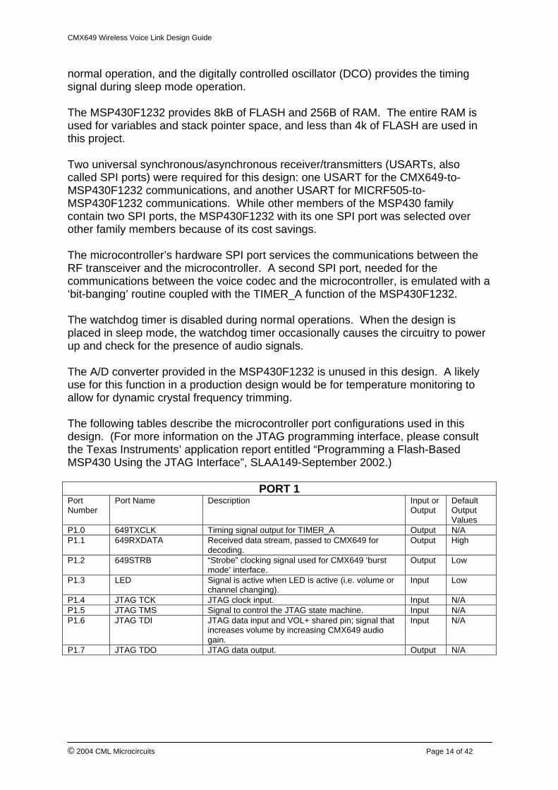
normal operation, and the digitally controlled oscillator (DCO) provides the timing signal during sleep mode operation. The MSP430F1232 provides 8kB of FLASH and 256B of RAM. The entire RAM is used for variables and stack pointer space, and less than 4k of FLASH are used in this project. Two universal synchronous/asynchronous receiver/transmitters (USARTs, also called SPI ports) were required for this design: one USART for the CMX649-to-MSP430F1232 communications, and another USART for MICRF505-to-MSP430F1232 communications. While other members of the MSP430 family contain two SPI ports, the MSP430F1232 with its one SPI port was selected over other family members because of its cost savings. The microcontroller’s hardware SPI port services the communications between the RF transceiver and the microcontroller. A second SPI port, needed for the communications between the voice codec and the microcontroller, is emulated with a ‘bit-banging’ routine coupled with the TIMER_A function of the MSP430F1232. The watchdog timer is disabled during normal operations. When the design is placed in sleep mode, the watchdog timer occasionally causes the circuitry to power up and check for the presence of audio signals. The A/D converter provided in the MSP430F1232 is unused in this design. A likely use for this function in a production design would be for temperature monitoring to allow for dynamic crystal frequency trimming. The following tables describe the microcontroller port configurations used in this design. (For more information on the JTAG programming interface, please consult the Texas Instruments’ application report entitled “Programming a Flash-Based MSP430 Using the JTAG Interface”, SLAA149-September 2002.)
PORT 1 Port Number
Port Name Description Input or Output
Default Output Values
P1.0 649TXCLK Timing signal output for TIMER_A Output N/A P1.1 649RXDATA Received data stream, passed to CMX649 for
decoding. Output High
P1.2 649STRB “Strobe” clocking signal used for CMX649 ‘burst mode’ interface.
Output Low
P1.3 LED Signal is active when LED is active (i.e. volume or channel changing).
Input Low
P1.4 JTAG TCK JTAG clock input. Input N/A P1.5 JTAG TMS Signal to control the JTAG state machine. Input N/A P1.6 JTAG TDI JTAG data input and VOL+ shared pin; signal that
increases volume by increasing CMX649 audio gain.
Input N/A
P1.7 JTAG TDO JTAG data output. Output N/A

CMX649 Wireless Voice Link Design Guide
© 2004 CML Microcircuits Page 15 of 42
PORT 2 Port Number
Port Name Description Input or Output
Default Output Values
P2.0 ACLK CMX649 xtal/clk input. Output N/A P2.1 VOL - Signal that decreases volume by decreasing
CMX649 audio output gain. Input N/A
P2.2 CHNL Signal that causes a change in RF channel by adjusting MICRF505 synthesizer programming.
Input N/A
P2.3 649RPLY CMX649 CBUS interface: “reply data” to the microcontroller.
Input N/A
P2.4 649RXCLK CMX649 “burst clock” signal applied to RX CLK pin.
Output low
P2.5 MICR505_CS MICRF505 “chip select” signal. Output low P2.6 Not present on MSP430F1232 P2.7 Not present on MSP430F1232
PORT 3 Port Number
Port Name Description Input or Output
Default Output Values
P3.0 BATT_SENSE Signal corresponding to battery voltage, to be used with battery recharging circuit (not included in this design).
Input N/A
P3.1 MICR505_DATAIXO MICRF505 data interface; SPI output line (‘slave in master out).
Output N/A
P3.2 MICR505_DATAIXO MICRF505 data interface; SPI output line (‘slave out master in’).
Input N/A
P3.3 MICR505_DATACLK MICRF505 data interface; clock input line. Output N/A P3.4 649TXDATA CMX649 encoded data output. Input N/A P3.5 649CSN CMX649 CBUS interface: “chip select” line. Output High P3.6 649_505_SCLK Serial clock signal for both the CMX649 “SCLK”
(CBUS interface) and the MICRF505 “SCLK” (control interface).
Output Low
P3.7 649_505_CMD Command data signal for both the CMX649 “CMD” (CBUS interface) and the MICRF505 “IO” (control interface).
Output Low
Table 2, Microcontroller Port Mapping
Connector J1 provides connections to the microcontroller’s JTAG interface to allow the device to be reprogrammed and debugged using the Texas Instruments MSP430 Flash Emulation Tool MSP-FETP430IF (not provided).
4.3.1 Data Buffering Scheme The general flow of data in this design is summarized in the following diagram:
CMX649Voice Codec
SPI-Rx RXRF_BUF
SPI-Tx RXTF_BUFManchesterEncoding
ManchesterDecoding
83.3kbps166.6kbps
MSP430F1232Microcontroller
MICRF505RF Transceiver 27.7kbps166.6kbps
Figure 4, Data Processing Flow Path

CMX649 Wireless Voice Link Design Guide
© 2004 CML Microcircuits Page 16 of 42
Data is exchanged between the RF transceiver and the microcontroller in a half-duplex fashion via the microcontroller’s SPI port. Data is transferred in a full-duplex fashion, however, between the microcontroller and the ‘burst mode’ interface of the CMX649. A large difference exists between the CMX649 voice coding rate (27.8kbps) and the over-the-air baud rate used by the MICRF505 (166.6kbps). If the RF transmitter and CMX649 were activated at the same time, the RF transmitter would transmit the data faster than the CMX649 could generate the data, and an underflow condition would quickly occur. In a similar manner, the 166.6kbps received data from the transceiver would quickly overwrite data being sent to the CMX649 at 27.8kbps. To manage the speed mismatches and prevent data overwrites/underwrites, a buffering scheme is implemented in the microcontroller. Eighty bytes of RAM in the MSP430F1232 are used as data buffers for both transmit (“RFTX_BUF”) and receive (“RFRX_BUF”) modes. Two microcontroller registers are used as counters to track the flow of data in and out of RFTX_BUF. These counters, called FROM649_CNTR and TORF_CNTR, are set to their maximum values when the transmit mode is first started. The FROM649_CNTR counter is decremented with each byte of encoded voice data that is passed from the CMX649 to the MSP430F1232. As the RFTX_BUF fills up, the FROM649_CNTR decreases in value. When the FROM649_CNTR decreases to the correct value, configuration data is loaded to the MICRF505 and the RF transmitter is enabled.
180
Data input from CMX649
Data output toMICRF505
79 34
RF transmissionbegins
RFTX_BUF byte location
Manchester Encoding
FROM649_CNTRat maximum value
FROM649_CNTRat minimum value
Figure 5, RFTX_BUF Byte Locations
After the RF transceiver is configured and enabled, the following header information is passed from the microcontroller to the transceiver:
• Bit sync (12 bytes) • Frame sync (2 bytes) • Command information (2 bytes) • Identification information (2 bytes)
The voice data and header information is Manchester encoded in the microcontroller; this is done to add sufficient transitions to the data signal to prevent the PLL from

CMX649 Wireless Voice Link Design Guide
© 2004 CML Microcircuits Page 17 of 42
attenuating the signal. The Manchester encoding is performed by splitting the bytes into nibbles, which are then mapped into a lookup table to obtain the appropriate Manchester-encoded value. A four-bit nibble will be converted into an eight-bit byte after Manchester encoding, therefore, the use of Manchester encoding effectively doubles the amount of data transmitted over the RF link:
Raw binary data nibble
Manchester encoded binary
data
Resulting hex value
0000 10101010 AA 0001 10101001 A9 0010 10100110 A6 0011 10100101 A5 0100 10011010 9A 0101 10011001 99 0110 10010110 96 0111 10010101 95 1000 01101010 6A 1001 01101001 69 1010 01100110 66 1011 01100101 65 1100 01011010 5A 1101 01011001 59 1110 01010110 56 1111 01010101 55
Table 3, Mapping of TX Data to Manchester encoded data
The data is then passed to the MICRF505 for transmission via the microcontroller’s USART0. The TORF_CNTR is decremented for each byte of data that is passed from the microcontroller to the MICRF505. When the last byte of data is transferred out of RFTX_BUF, both FROM649_CNTR and TORF_CNTR have achieved their minimum values. A four-byte ‘dummy’ packet is passed to the MICRF505 to ensure that all of the actual data has been transmitted, and the microcontroller prepares the transceiver for receive operation. In receive mode, the recovered data is passed from the transceiver to the microcontroller’s USART0 receive buffer, and then to an eighty-byte section of RAM referred to as “RFRX_BUF”. Two microcontroller registers are used as counters to track the flow of data in and out of RFRX_BUF. These counters, called FROMRF_CNTR and TO649_CNTR, are set to their maximum values when the receive mode is first started. The FROMRF_CNTR counter is decremented by one for each byte of data that is passed from the transceiver to the microcontroller. The TO649_CNTR counter is decremented by one for each byte of data that is passed from the microcontroller to the CMX649.

CMX649 Wireless Voice Link Design Guide
© 2004 CML Microcircuits Page 18 of 42
Data input from MICRF505 Data output to
CMX649
RFRX_BUF byte location
Manchester Decoding
1 80 79
TO649_CNTR at minimum value
TO649_CNTR atmaximum value
Figure 6, RFRX_BUF Byte Locations
The first information that is received corresponds to header information; this information is not intended for decoding and is not passed to the CMX649. Once the header is recognized, the subsequent received bytes are passed to the CMX649 for voice signal reconstruction. Since the transceiver is operating at a much higher data rate than the CMX649, the data will flow into the RFRX_BUF faster than it is sent out to the CMX649. Once the first data byte is loaded into the RFRX buffer, data can be transferred to the CMX649 with no risk of data underflow.
4.4 Battery The battery chosen for this design is an Ultralife UBC 641730 lithium-polymer rechargeable battery. Lithium-ion polymer technology was chosen for this project because of its exceptional energy density and its ability to withstand multiple charge/discharge cycles with no “memory effect”. This particular battery was chosen because of its very small form factor and sizeable energy capacity. The current consumption of this design is dependent on many factors, including how often the user speaks into the unit, the volume with which the user speaks, the volume setting for the unit’s speaker, and the RF power setting. The observed value for current consumption during normal conversation is 19.25mA, which translates to a “talk time” of approximately 10.4 hours. The observed current consumption for sleep mode is 140µA, which translates to a “standby time” of approximately 60 days. (Note: these values are based on 100% battery capacity being available for use, but the low discharge rate of this design makes this assumption reasonably accurate.) The battery voltage is monitored by microcontroller P3.0. This function, when paired with a user-supplied algorithm, can detect low battery voltage and powerdown the circuitry to prevent excessive discharge and battery damage. The Ultralife UBC 641730 lithium-polymer battery includes a protection module that guards against excessive current discharge, overvoltage and undervoltage conditions. Please consult your battery vendor to learn if your lithium-based battery contains such a protection module, and if not, the steps you must take to ensure safe product operation.

CMX649 Wireless Voice Link Design Guide
© 2004 CML Microcircuits Page 19 of 42
Lithium-based batteries provide many benefits, but the technology that yields these benefits requires special care and precaution, especially with regards to operating voltage, operating temperature, current discharge rate and recharging. In particular, lithium-based batteries can be damaged if excessive discharge occurs, or if an over/undervoltage condition is allowed to develop. Many lithium-based batteries are supplied with protection circuitry that is designed to prevent these harmful conditions. Please consult the battery vendor for more information on care, operation, and recharging issues related to lithium-based batteries. The battery circuit is configured to easily accommodate an external, user-supplied charging circuit. Vendors such as Micrel, Maxim, National Semiconductor, Texas Instruments and others supply integrated circuits that can form the foundation of a battery charging circuit. A Micrel MIC79110 1.2A linear Li-Ion battery charger demonstration board was used in the development work for this project. Information on the Micrel MIC79110 integrated circuit and demonstration board can be found at:
www.micrel.com. For more information on this battery and related battery charging issues, please visit:
www.ultralifebatteries.com.
4.5 Voltage Regulators Two low-voltage dropout (LDO) regulators from Maxim are used in this design. The low-noise MAX8510EXK25 is used to translate the nominal 3.7V battery voltage to 2.5V for the RF transceiver, and the low-noise MAX8511EXK33 produces the 3.3V for the other integrated circuits. These products were chosen because of their low noise performance, small size and low cost. For more information on these products, please visit:
www.maxim-ic.com.
4.6 Peripheral Functions Two approaches were considered for the timing source used in this design. Each approach offers costs and benefits, and the end customer must make the determination regarding which approach best suits their requirements:
• A 16MHz crystal for the RF transceiver and an 8MHz crystal for the microcontroller and voice codec.
• An 8MHz crystal for the RF transceiver, microcontroller and voice codec The first approach uses two crystals, one for the RF transceiver and the other for the voice codec and microcontroller. This approach would yield a slight improvement in adjacent channel rejection, at a cost of the additional crystal, load capacitors, and required board space. The second alternative is the use of a single 8MHz crystal for the RF transceiver, microcontroller, and voice codec. This approach represented the optimal trade-off

CMX649 Wireless Voice Link Design Guide
© 2004 CML Microcircuits Page 20 of 42
between performance and costs and was therefore selected as the timing source for this project. Temperature monitoring is not performed in this design. The expectation is that the end customer can pair their own algorithm with the ADC capability afforded by the MSP430F1232 microcontroller to efficiently perform this function.
5 Firmware Description The firmware used for the Master board is different than that used in the Slave board, but both have the same basic structure. The firmware controls the CMX649 voice codec, the RF transceiver, and the transfer of data between them. The master board synchronizes all communications. The Master board’s firmware takes advantage of the CMX649’s programmable voice activity detector (VAD) to determine when voice/audio is present. This allows the Master board to decide when to power save (i.e. after periods where voice/audio is consistently absent), and when to wake from power save (i.e. when voice/audio has been detected). The firmware source code for this project was written in assembly language and was compiled using the IAR Embedded Workbench from IAR Systems. More information concerning the IAR Embedded Workbench can be found at:
http://www.iar.com/Products/EW/ The source code used in this project can be downloaded from the CML website at:
www.cmlmicro.com/products/applications/649/DE6492.zip The firmware can be reprogrammed using the JTAG programming port (P1.4-1.7), if desired. More MSP430F1232 programming information can be found in the following resources:
1. Texas Instruments’ application report “Programming a Flash-Based MSP430 Using the JTAG Interface”, SLAA149-September 2002.
2. Texas Instruments’ document “MSP430x1xx Family User’s Guide”, SLAU049C, 2003.

CMX649 Wireless Voice Link Design Guide
© 2004 CML Microcircuits Page 21 of 42
5.1.1 Interrupt Vectors Interrupt vectors for this project are as follows: Interrupt Name Vectored Interrupt Service
Routine Comments
RESET_VECTOR RESET (initialization routine) Issued on power up. UART0TX_VECTOR RFCHIPTX Called when ready to Tx
a new byte. UART0RX_VECTOR RFCHIPRX Called once a byte has
been received. TIMERA0_VECTOR CMX649_TRANSFER Called when ready to
exchange data with the CMX649.
PORT1_VECTOR and PORT2_VECTOR
BUTTON_DEBOUNCE Debounce routine
Table 4, Interrupt Vectors
5.1.2 RESET When the circuit is powered up, the MSP430F1232 will begin program execution at the RESET initialization routine, which is depicted in the following flowchart:

CMX649 Wireless Voice Link Design Guide
© 2004 CML Microcircuits Page 22 of 42
From dev ice reset
Reset v olumeand RF channel
Initialize uCStack Pointer
Stop Watchdog Timer
Conf igure uCI/O ports
CallPWR_RF_OSC
Change uC timingsource f rom DCO
to cry staloscillator
Conf igure uCclock sy stem
Clear uCoscillator f aultinterrupt f lag
Wait until cry stalhas stabilized
Stop uC DCOclock
Conf igure uCUSART0
Setup uC TimerA
Initialize Master &Slav e IDs
Initialize countersf or v oice codec& RF transceiv er
Conf igure blocksy nchronization
CallSETUP649
Initialize preamblecounter
Initialize programstatus f lags
Clear uCPort 1 & Port 2
interrupts
CallUPDATE649_VOL
CallSETUPRF and
leav e in standby
Initializecommands f or
Master & Slav e
Enable allinterrupts
Jump toMAINLOOP
Figure 7, RESET Initialization Routine
Control is passed to the MAINLOOP routine upon completion of the RESET initialization routine.

CMX649 Wireless Voice Link Design Guide
© 2004 CML Microcircuits Page 23 of 42
5.1.3 SETUP649 The SETUP649 subroutine, called by the RESET initialization routine, preconfigures the CMX649 for audio processing. A ‘general reset’ is first performed to place the CMX649 internal registers in a defined state. After the reset is performed and a suitable delay is observed to allow the device to stabilize, the CMX649 is configured as follows:
CMX649 Register
Register Contents
Comments
0x61 0x00 AAF & AIF bandwidth=2.9kHz. 0x63 0x80 Audio input gain=0.0dB. 0x64 0x55 AAF & AIF power control=normal operation, encode & decode
DAC=lowest power setting. 0x65 0x95 Microphone amp=low power, audio DCA & volume DCA=lowest power. 0x70 0x01 ADM mode with buffered I/O (i.e. 8-bit burst mode). 0x71 0x0014 Scrambler disabled. 0x72 0xEC52 Configured to yield 27.8kbps sampling rate from 8MHz crystal. 0x73 0x0078 Encode & decode bit clocks (i.e. sampling clocks) derived from xtal/clk
input. 0x81 0x88 No encoder or decoder IRQs. 0xD0 0x00BE ADM decoder configured for normal operation, decode VAD output
driven to 1 to activate microphone circuit (DECVAD pin controls FET that stops current flow to the microphone when required.)
0xD1 0x4999 Syllabic time constant=1.2ms, 4 of 4 companding rule, estimator time constant = 0.8ms, second order integration.
0xE0 0xBC ADM encoder configured for normal operation, encode VAD output driven to 0 to activate audio amplifier (ENCVAD pin supplies ‘shutdown’ signal to audio amplifier.)
0xE1 0x499A Syllabic time constant=1.2ms, 4 of 4 companding rule, estimator time constant = 0.8ms, second order integration.
Table 5, CMX649 Configuration in SETUP649 Subroutine
Control reverts back to the RESET initialization routine after the CMX649 initialization is complete.
5.1.4 SETUPRF The SETUPRF subroutine, which is called by the RESET initialization routine, preconfigures the MICRF505 for either transmission or reception. Further configuration is made in the appropriate transmit or receive subroutines.

CMX649 Wireless Voice Link Design Guide
© 2004 CML Microcircuits Page 24 of 42
Highlights of the configuration performed in SETUPRF include: MICRF505
Control Register
Register Contents
Comments
0x00 0x03 Device in standby mode. 0x01 0x0F Closed loop modulation using modulator, Lock Detect enabled, 340kHz
Sallen-Key filter bandwidth. 0x02 0x50 125µA charge pump current, main channel filter bypassed, power
amplifier bypassed. 0x03 0xCD VCO free-running frequency = 868MHz. 0x04 0x3B MOD_F=1, MOD_I=27. 0x05 0x11 MOD_A=1. 0x06 0x6E Mod_clkS=6, BitSync_clkS=14. 0x07 0xC3 BitRate_clkS=3, RefClk_K=3. 0x08 0xC1 ScClk_X2=1, ScClk=1. 0x0A 0x0E A0=14. 0x0B 0x00 0x0C 0x6B
N0=107.
0x0D 0x00 0x0E 0x10
M0=16.
Table 6, MICRF505 Configuration in SETUPRF Subroutine
The setting for control register 0x3F (XCO tuning register) is dependent on the amount of tuning required for the crystal oscillator circuit, and as such, is application dependent.
5.1.5 MAINLOOP The MAINLOOP checks the PROG_FLAGS variable to see if the device needs to be transmitting or receiving. Once this decision has been made, the firmware jumps to the transmit or receive configuration subroutines (START_RFTX or START_RFRX). The MAINLOOP routine is illustrated in the following flowchart:

CMX649 Wireless Voice Link Design Guide
© 2004 CML Microcircuits Page 25 of 42
Switch to TX?
f rom RESET orAudio/RF sense
No
Yes
Switch to RX?
Yes
No
CallSTART_RFTX
CallLEDFLASH
CallSTART_RFRX
Figure 8, MAINLOOP Routine
When a byte is ready for transmission, or if a received byte is ready for microcontroller processing, the USART transmit or receive interrupt will occur and the firmware will vector to either the RFCHIPTX or RFCHIPRX subroutines. If no USART interrupts occur, the MAINLOOP routine loops back onto itself.
5.1.6 START_RFTX When the START_RFTX subroutine is called, the transmit flag bit in the PROG_FLAGS variable is cleared, the SPI port is primed with 0xAA and the preamble counter is initialized to 48, which is the number of preamble bytes to be sent after the transmitter is enabled. The output buffer counter, TORF_CNTR, is initialized to 84 (counter range is from 83 to 0) and the SET_RF_TX subroutine is called. When the SET_RF_TX subroutine has finished, the USART0 transmit interrupt is enabled, and control reverts back to the MAINLOOP routine.
5.1.7 SET_RF_TX When the “SET_RF_TX” subroutine is called, MICRF505 control register 0x00 is manipulated to enable transmit operation in synchronous mode. Microcontroller Port 3 is then configured as follows:

CMX649 Wireless Voice Link Design Guide
© 2004 CML Microcircuits Page 26 of 42
Port Number Schematic Name Function P3.0 BATT_SENSE Analog input to 10-bit ADC P3.1 MICR505_DATAXIO SPI port: ‘slave in, master out’ P3.2 MICR505_DATAXIO SPI port: ‘slave out, master in’ P3.3 MICF505_DATCLK SPI port; clock input P3.4 649TXDATA General I/O P3.5 649CSN General I/O P3.6 649_505_SCLK General I/O P3.7 649_505_CMD General I/O
Table 7, Microcontroller Port 3 Configuration in SET_RF_TX Subroutine
A 750µs pause is inserted to allow the RF transceiver’s PLL to stabilize, after which time the subroutine ends and control is transferred back to the START_RFTX subroutine.
5.1.8 RFCHIPTX An interrupt is issued in transmit mode when a byte of data can be written to the USART0 transmit buffer. When this interrupt occurs, the firmware vectors to the RFCHIPTX interrupt service routine (ISR). The RFCHIPTX ISR first determines if the entire amount of preamble has already been transmitted. If the preamble transmission isn’t complete, the firmware then determines if preamble or frame sync words remain to be transmitted. Once this determination is made, the appropriate byte is loaded into the microcontroller’s USART0 transmit buffer, and the ISR returns from interrupt. The RFCHIPTX ISR is illustrated in the following flowchart:

CMX649 Wireless Voice Link Design Guide
© 2004 CML Microcircuits Page 27 of 42
Preamblefinished?
No
Return frominterrupt
from interrupt
Load preamblebyte into uC TX
buffer
Upper nibblealready sent?
Yes
Preamblecounter < 3?
No
Decrementpreamble counter
YesDecrementpreamble counter
Copy preamblecounter to R6
Place appropriatesync word in uC
TX buffer
Return frominterrupt
Yes
No
Copy next byte tobe transmitted into
R6
Shift upper nibbleof R6 into lowernibble position
Set flag indicatingupper nibble has
been sent
Mask upper nibbleof R6
Manchesterencode R6 value,place result in uC
TX buffer
Have all bytesbeen sent?
Return frominterrupt
Yes
No
Copy next byte tobe transmitted into
R6
Clear flag toindicate upper
nibble needs to besent
DecrementTORF_CNTR
Disable Tx and Rxinterrupts
Return frominterrupt
Set flag to enableRx
Figure 9, RFCHIPTX Interrupt Service Routine

CMX649 Wireless Voice Link Design Guide
© 2004 CML Microcircuits Page 28 of 42
Once the preamble and frame sync words have been transmitted, the firmware begins to write audio data bytes to the SPI transmit buffer. The data bytes are split into nibbles, and the upper nibble is the first to be Manchester encoded and loaded into the USART0 transmit buffer. (Note that a four-bit nibble, once Manchester encoded, becomes an eight-bit byte.) After both the upper and lower nibbles of the data byte have been transmitted, the ISR checks the progression of the data frame transmission. If the data frame isn’t complete, the ISR returns from interrupt. If the data frame is complete, transmit and receive USART interrupts are disabled, a flag is set to indicate that the RF transceiver needs to enter receive mode, and the ISR returns from interrupt.
5.1.9 START_RFRX When START_RFRX is called, Microcontroller Port 3 is configured as follows: Port Number Schematic Name Function P3.0 BATT_SENSE Analog input to 10-bit ADC P3.1 MICR505_DATAXIO SPI port: ‘slave in, master out’ P3.2 MICR505_DATAXIO General I/O P3.3 MICF505_DATCLK SPI port; clock input P3.4 649TXDATA General I/O P3.5 649CSN General I/O P3.6 649_505_SCLK General I/O P3.7 649_505_CMD General I/O
Table 8, Microcontroller Port 3 Configuration in START_RFRX Subroutine
The receive flag bit in the PROG_FLAGS variable is cleared and the input buffer counter (FROMRF_CNTR) is initialized to 84. The sync word flags in the PROG_FLAGS variable are set to indicate that both sync words need to be received. The upper nibble flag is cleared to indicate that the upper nibble has not been received. The master and slave IDs are compared to ensure they no longer match before attempting to receive a new frame, and the SET_RF_RX subroutine is called. When control is passed back to the START_RFRX subroutine, the preamble counter is set to 24, which is the number of preamble bytes that are skipped after turning on the RF receiver. A counter used to limit the time for the frame sync byte search is initialized, and the USART0 receive interrupt is enabled. A check is made regarding the status of Sync Word 2, and the subroutine returns control to the MAINLOOP if Sync Word 2 has been received. If Sync Word 2 hasn’t been received yet, a check is made regarding whether or not Tx mode has been enabled; if it has, the subroutine again checks the status of Sync Word 2. If Tx mode has been enabled, the subroutine returns control to the MAINLOOP routine. The START_RFRX subroutine is illustrated in the following flowchart:

CMX649 Wireless Voice Link Design Guide
© 2004 CML Microcircuits Page 29 of 42
from MAINLOOP
Configure uCPort 3
Clear RX flag
Reset Input BufferCounter
(FROMRF_CNTR)
Set flags toindicate syncwords not yet
received
Clear flag toindicate uppernibble received
Ensure Master &Slave IDs nolonger match
CallSET_RF_RX
Initialize preambleand Rx duration
counters
Has SyncWord 2 been
received?
No
Return
Enable Rxinterrupt
Yes
Has Tx modebeen enabled?
Yes
No
Figure 10, START_RFRX Subroutine

CMX649 Wireless Voice Link Design Guide
© 2004 CML Microcircuits Page 30 of 42
5.1.10 SET_RF_RX When the “SET_RF_RX” subroutine is called, 0x0D is written to MICRF505 control register 0x00 to enable receive operation in synchronous mode. Next, 0x0F is written to control register 0x01 to activate the lock detect function and to select 340kHz for the Sallen-Key low-pass filter bandwidth. A 250µs delay is inserted to allow the RF transceiver’s PLL to settle, and the subroutine ends with control reverting back to the START_RFRX subroutine.
5.1.11 RFCHIPRX When a byte of data has been received by the RF transceiver and the microcontroller’s USART0 receive interrupt is issued, the firmware vectors to the RFCHIPRX interrupt service routine. The newly received byte is copied into the R6 register and a check is made to see if the expected amount of preamble has already been received. In other words, a check is made regarding whether the newly received byte is likely preamble or something else. If more preamble is expected, the received byte is likely preamble information and not real data, so the PREAMBLE_COUNTER is decremented and the subroutine returns from interrupt. If the PREAMBLE_COUNTER is zero, the entire expected preamble has already been received, which means the received byte is likely meaningful data. In this case, processing of the received byte begins. The two most recently received data bytes are assembled into a data word, the shift counter is reset to zero, and a test is performed to see if Sync Word 1 has already been received. If Sync Word 1 has not yet been received, the subroutine shifts the data word one bit position, increments the shift counter, and compares the new data word to the expected sync word. If a match is found, a flag is cleared to indicate that Sync Word 1 is no longer needed, the number of required bit shifts is stored for future reference, and the subroutine returns from interrupt. If the shifted data word does not match Sync Word 1, the subroutine shifts the data word another bit position and performs another comparison so long as eight bit shifts have not already occurred. If eight bit shifts have already been performed without a match being found, the data word is deemed garbage data and the subroutine returns from interrupt. When the firmware determines that Sync Word 1 has already been received, the shift counter value is used to synchronize the data word in R6 and R7 along byte boundaries. A test is performed to determine if Sync Word 2 has already been received. If Sync Word 2 is yet to be received, R7 is immediately compared to the expected Sync Word 2 value. A negative result to this test means that a new search for frame sync is needed, so the firmware will set flags indicating that both sync words are needed and the subroutine returns from interrupt. A positive result to this test causes a flag to be cleared, indicating that Sync Word 2 has been found, and buffer pointers are properly aligned. The subroutine then returns from interrupt. When a data byte has been received and both Sync Words have already been processed, the byte is presumed to be actual audio data and the firmware begins the

CMX649 Wireless Voice Link Design Guide
© 2004 CML Microcircuits Page 31 of 42
process of Manchester decoding. The properly aligned data byte is divided by two, mapped to a Manchester lookup table, and the decoded value is placed in the R6 register. Since Manchester encoding doubles the amount of data needed for a transaction, an eight-bit Manchester encoded byte actually includes only four bits of ‘real’ data. For this reason, the decoded data byte is effectively split into upper and lower nibbles and processed accordingly. A flag is used to indicate whether the upper or lower nibble is needed, and once both nibbles have been decoded, the FROMRF_CNTR is decremented. Transmit and receive interrupts are disabled when FROMRF_CNTR becomes negative, as this indicates that the expected number of data bytes have been received and the incoming data frame is complete. The RFCHIPRX ISR is illustrated in the following flowchart:

CMX649 Wireless Voice Link Design Guide
© 2004 CML Microcircuits Page 32 of 42
Sy nc By te 1already
receiv ed?
No
Yes
No
Yes
Copy new Rx'd by teto R6
f rom interrupt
B
Decrement preamblecounter
Has enoughpreamble been
receiv ed?
Return f rominterrupt
Place two most recentRx'd by tes into R6 &
R7 (assemble into dataword)
Reset Shif t Counter(R10)
Sy nchronize currentand last Rx'd by tes on
by te boundaries
Sy nc By te 2already
receiv ed?
Yes
No
C
Load number of shif tsrequired to align by tes
A
Figure 11, RFCHIPRX Interrupt Service Routine

CMX649 Wireless Voice Link Design Guide
© 2004 CML Microcircuits Page 33 of 42
Clear f lag to indicateSy nc By te 1 has been
f ound
R7 = Sy nc By te1?
Store number of shif tsrequired to sy nc Rx'd
by tes
Return f rominterrupt
Yes
NoHav e 8 bit shif tsoccurred?
No
Yes
Return f rominterrupt
A
Div ide R7 by two,mask of f
upper two bits
Upper nibblealready
decoded?
Perf orm Manchesterdecoding on R7 v alue,
place result in R6
No
Mask of f lower nibbleof Manchester decoded
v alue in R6
Mov e R6 upper nibbleto RXRF_BUF
Set f lag indicatingupper nibble already
decoded
Return f rominterrupt
Mask of f upper nibbleof Manchester decoded
v alue in R6
Yes
Add R6 lower nibble toRXRF_BUF
Clear f lag to indicateupper nibble not
decoded
DecrementFROMRF_CNTR
E
Shif t R6 & R7 by tesby one bit
Increment Shif t Counter
C B
B
Figure 12, RFCHIPRX Interrupt Service Routine (continued)

CMX649 Wireless Voice Link Design Guide
© 2004 CML Microcircuits Page 34 of 42
IsFROMRF_CNTR
negativ e?
Return f rominterrupt
Disable Tx and Rxinterrupts
E
No
Yes
Return f rominterrupt
B
Return f rominterruptClear f lag to indicate
Sy nc By te 2 has beenf ound
Align pointers tosy nchronize master &
slav e timing
R7 = Sy nc By te2 ?
Yes
Return f rominterrupt
Set f lags to indicateSy nc By te 1 & 2 are
still needed
No
Figure 13, RFCHIPRX Interrupt Service Routine (continued)
5.1.12 CMX649_TRANSFER The MSP430F1232’s TIMER_A is used with a bit-banging routine to emulate a second SPI port for microcontroller-to-CMX649 communications. When the TIMER_A issues an interrupt, the CMX649_TRANSFER interrupt service routine is called. The master unit’s CMX649_TRANSFER ISR, which is responsible for handling all data transfer between the CMX649 and the microcontroller, is illustrated in the following flowchart (please note that the firmware for the master and slave units are only marginally different):

CMX649 Wireless Voice Link Design Guide
© 2004 CML Microcircuits Page 35 of 42
f rom interrupt
Clear TIMER_Ainterrupt
CallSYNC_SERVICE(bit bang routine)
DecrementFROM649_CNTR
Do Master &Slav e IDsmatch?
Send idle patternto CMX649
No
Yes
A
No Rx durationcounter expired?
Yes
Decrementduration counter
NoVolume
debouncecounterexpired?
Yes
Decrementv olume debounce
counter
NoChannel
debouncecounterexpired?
Yes
Decrementchannel debounce
counter
Figure 14, CMX649_TRANSFER Interrupt Service Routine

CMX649 Wireless Voice Link Design Guide
© 2004 CML Microcircuits Page 36 of 42
A
ResetFROM649_CNTR
Return f rominterrupt
DecrementTO649_CNTR FROM649_CNTR
= 35?Yes
No
DecrementTO649_CNTR
Set f lag to startTx
Is TO649_CNTRnegativ e?
Return f rominterrupt
No
Yes
Yes Is RFTX_BUFf ull?
No
ResetTO649_CNTR
Reset dev ice pairchecking
parameters
Return f rominterrupt
Figure 15, CMX649_TRANSFER Interrupt Service Routine (continued)
6 Circuit Schematics and Board Layout The schematics and board layout files for this project were created using P-CAD. These files are available for download from the CML website at:
www.cmlmicro.com/products/applications/649 The size of the board containing this design is 2.5 x 3.3 cm (1.0 x 1.3in). This small size is consistent with a wireless headset form factor, but it is possible to shrink the board size even more with smaller components and tighter spacing.

CMX649 Wireless Voice Link Design Guide
© 2004 CML Microcircuits Page 37 of 42
5VOUT
4BP
3 SHDN1 VIN+
2 GND
5Vout
4NC
1 Vin3 SHDN
2 Gnd
21
Figure 16, Microcontroller Section

CMX649 Wireless Voice Link Design Guide
© 2004 CML Microcircuits Page 38 of 42
1
3
2
Figure 17, Voice Codec Section

CMX649 Wireless Voice Link Design Guide
© 2004 CML Microcircuits Page 39 of 42
Figure 18, RF Transceiver Section

CMX649 Wireless Voice Link Design Guide
© 2004 CML Microcircuits Page 40 of 42
7 Bill of Materials The following table lists the materials used in this design.
Table 9, Bill of Materials

CMX649 Wireless Voice Link Design Guide
© 2004 CML Microcircuits Page 41 of 42
8 Conclusion The CMX649 can form the core of an inexpensive, small form factor, and low power consumption wireless voice platform that can serve in a variety of applications. This document has presented one such design that can be easily modified to suit various design objectives. It is hoped that the information presented in this document will assist customers who wish to design these types of applications.
CML does not assume any responsibility for the use of any circuitry described. No IPR or circuit patent licences are implied. CML reserves the right at any time without notice to change the said circuitry and this product specification. CML has a policy of testing every product shipped using
calibrated test equipment to ensure compliance with this product specification. Specific testing of all circuit parameters is not necessarily performed.
www.cmlmicro.com For FAQs see: http://www.cmlmicro.com/products/faqs/index.htm
For a full data sheet listing see: http://www.cmlmicro.com/products/datasheets/download.htm
For detailed application notes: http://www.cmlmicro.com/products/applications/index.htm
Oval Park, Langford, Maldon, Essex, CM9 6WG - England. Tel: +44 (0)1621 875500 Fax: +44 (0)1621 875600 Sales: [email protected] Technical Support: [email protected]
4800 Bethania Station Road, Winston-Salem, NC 27105 - USA. Tel: +1 336 744 5050, 800 638 5577 Fax: +1 336 744 5054 Sales: [email protected] Technical Support: [email protected]
No 2 Kallang Pudding Road, 09 to 05/06 Mactech Industrial Building, Singapore 349307 Tel: +65 7450426 Fax: +65 7452917 Sales: [email protected] Technical Support: [email protected]
No. 218, Tian Mu Road West, Tower 1, Unit 1008, Shanghai Kerry Everbright City, Zhabei, Shanghai 200070, China. Tel: +86 21 63174107 +86 21 63178916 Fax: +86 21 63170243 Sales: [email protected] Technical Support: [email protected]

CMX649 Wireless Voice Link Design Guide
© 2004 CML Microcircuits Page 42 of 42