Embed Size (px)
Citation preview
This is information on a product in full production.
July 2016 DocID025449 Rev 8 1/35
M24C64S-FCU
64-Kbit serial I²C bus EEPROM 4 balls CSPDatasheet - production data
Features
• Compatible with the 400 kHz I²C protocol
• High speed 1MHz transfer rate
• Memory array:
– 64 Kbit (8 Kbyte) of EEPROM
– Page size: 32 byte
• Supply voltage range:
– 1.7 V to 5.5 V
• Operating temperature range
– VCC = 1.7 V to 5.5V over -40°C / +85°C
– VCC = 1.6 V to 5.5V over 0°C / +85°C
• Write
– Byte Write within 5 ms
– Page Write within 5 ms
• Random and sequential Read modes
• Software Write protect
– Upper quarter memory array
– Upper half memory array
– Upper 3/4 memory array
– Whole memory array
• ESD protection
– Human Body Model: 4 kV
• More than 4 million Write cycles
• More than 200-years data retention
• Package
– WLCSP, RoHS and Halogen free compliant (ECOPACK2®)
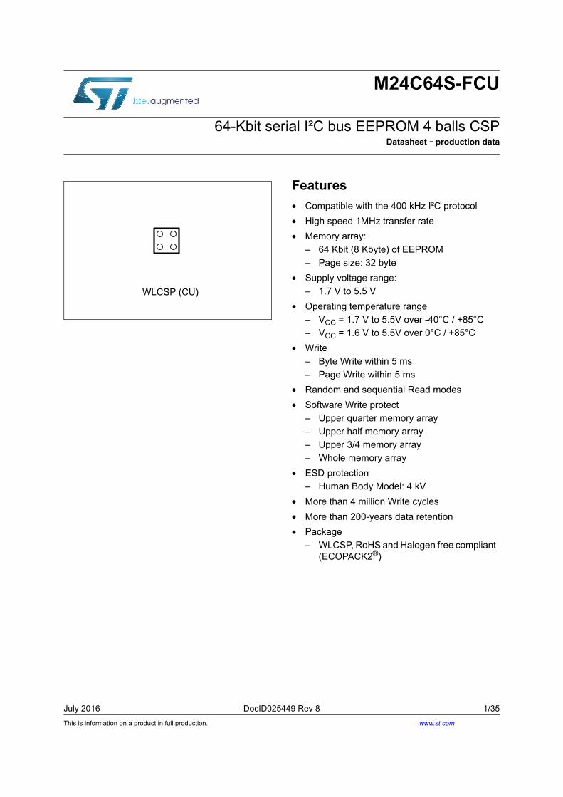
WLCSP (CU)
www.st.com
Contents M24C64S-FCU
2/35 DocID025449 Rev 8
Contents
1 Description . . . . . . . . . . . . . . . . . . . . . . . . . . . . . . . . . . . . . . . . . . . . . . . . . 6
2 Signal description . . . . . . . . . . . . . . . . . . . . . . . . . . . . . . . . . . . . . . . . . . . 7
2.1 Serial Clock (SCL) . . . . . . . . . . . . . . . . . . . . . . . . . . . . . . . . . . . . . . . . . . . 7
2.2 Serial Data (SDA) . . . . . . . . . . . . . . . . . . . . . . . . . . . . . . . . . . . . . . . . . . . . 7
2.3 VSS (ground) . . . . . . . . . . . . . . . . . . . . . . . . . . . . . . . . . . . . . . . . . . . . . . . 7
2.4 Supply voltage (VCC) . . . . . . . . . . . . . . . . . . . . . . . . . . . . . . . . . . . . . . . . . 7
2.4.1 Operating supply voltage (VCC) . . . . . . . . . . . . . . . . . . . . . . . . . . . . . . . . 7
2.4.2 Power-up conditions . . . . . . . . . . . . . . . . . . . . . . . . . . . . . . . . . . . . . . . . 7
2.4.3 Device reset . . . . . . . . . . . . . . . . . . . . . . . . . . . . . . . . . . . . . . . . . . . . . . . 7
2.4.4 Power-down conditions . . . . . . . . . . . . . . . . . . . . . . . . . . . . . . . . . . . . . . 8
3 Memory organization . . . . . . . . . . . . . . . . . . . . . . . . . . . . . . . . . . . . . . . . 9
4 Device operation . . . . . . . . . . . . . . . . . . . . . . . . . . . . . . . . . . . . . . . . . . . 10
4.1 Start condition . . . . . . . . . . . . . . . . . . . . . . . . . . . . . . . . . . . . . . . . . . . . . . .11
4.2 Stop condition . . . . . . . . . . . . . . . . . . . . . . . . . . . . . . . . . . . . . . . . . . . . . . .11
4.3 Data input . . . . . . . . . . . . . . . . . . . . . . . . . . . . . . . . . . . . . . . . . . . . . . . . . .11
4.4 Acknowledge bit (ACK) . . . . . . . . . . . . . . . . . . . . . . . . . . . . . . . . . . . . . . .11
4.5 Device addressing . . . . . . . . . . . . . . . . . . . . . . . . . . . . . . . . . . . . . . . . . . 12
5 Instructions . . . . . . . . . . . . . . . . . . . . . . . . . . . . . . . . . . . . . . . . . . . . . . . 13
5.1 Write operations . . . . . . . . . . . . . . . . . . . . . . . . . . . . . . . . . . . . . . . . . . . . 13
5.1.1 Byte Write . . . . . . . . . . . . . . . . . . . . . . . . . . . . . . . . . . . . . . . . . . . . . . . 14
5.1.2 Page Write . . . . . . . . . . . . . . . . . . . . . . . . . . . . . . . . . . . . . . . . . . . . . . . 15
5.1.3 Write protection . . . . . . . . . . . . . . . . . . . . . . . . . . . . . . . . . . . . . . . . . . . 16
5.1.4 Minimizing Write delays by polling on ACK . . . . . . . . . . . . . . . . . . . . . . 17
5.2 Read operations . . . . . . . . . . . . . . . . . . . . . . . . . . . . . . . . . . . . . . . . . . . . 18
5.2.1 Random Address Read . . . . . . . . . . . . . . . . . . . . . . . . . . . . . . . . . . . . . 18
5.2.2 Current Address Read . . . . . . . . . . . . . . . . . . . . . . . . . . . . . . . . . . . . . . 19
5.2.3 Sequential Read . . . . . . . . . . . . . . . . . . . . . . . . . . . . . . . . . . . . . . . . . . 19
5.2.4 Read the Write Protect register . . . . . . . . . . . . . . . . . . . . . . . . . . . . . . . 19
6 Initial delivery state . . . . . . . . . . . . . . . . . . . . . . . . . . . . . . . . . . . . . . . . . 20

DocID025449 Rev 8 3/35
M24C64S-FCU Contents
3
7 Maximum rating . . . . . . . . . . . . . . . . . . . . . . . . . . . . . . . . . . . . . . . . . . . . 21
8 DC and AC parameters . . . . . . . . . . . . . . . . . . . . . . . . . . . . . . . . . . . . . . 22
9 Package information . . . . . . . . . . . . . . . . . . . . . . . . . . . . . . . . . . . . . . . . 28
9.1 Ultra Thin WLCSP package information . . . . . . . . . . . . . . . . . . . . . . . . . . 28
10 Part numbering . . . . . . . . . . . . . . . . . . . . . . . . . . . . . . . . . . . . . . . . . . . . 32
11 Revision history . . . . . . . . . . . . . . . . . . . . . . . . . . . . . . . . . . . . . . . . . . . 34

List of tables M24C64S-FCU
4/35 DocID025449 Rev 8
List of tables
Table 1. Signal names . . . . . . . . . . . . . . . . . . . . . . . . . . . . . . . . . . . . . . . . . . . . . . . . . . . . . . . . . . . . 6Table 2. Device select code . . . . . . . . . . . . . . . . . . . . . . . . . . . . . . . . . . . . . . . . . . . . . . . . . . . . . . . 12Table 3. Most significant address byte . . . . . . . . . . . . . . . . . . . . . . . . . . . . . . . . . . . . . . . . . . . . . . . 13Table 4. Least significant address byte . . . . . . . . . . . . . . . . . . . . . . . . . . . . . . . . . . . . . . . . . . . . . . 13Table 5. Write Protect register (Address = 1xxx.xxxx.xxxx.xxxxb) . . . . . . . . . . . . . . . . . . . . . . . . . . 16Table 6. Absolute maximum ratings . . . . . . . . . . . . . . . . . . . . . . . . . . . . . . . . . . . . . . . . . . . . . . . . . 21Table 7. Test conditions . . . . . . . . . . . . . . . . . . . . . . . . . . . . . . . . . . . . . . . . . . . . . . . . . . . . . . . . . . 22Table 8. Operating conditions. . . . . . . . . . . . . . . . . . . . . . . . . . . . . . . . . . . . . . . . . . . . . . . . . . . . . . 22Table 9. DC characteristics. . . . . . . . . . . . . . . . . . . . . . . . . . . . . . . . . . . . . . . . . . . . . . . . . . . . . . . . 23Table 10. 400 kHz AC characteristics. . . . . . . . . . . . . . . . . . . . . . . . . . . . . . . . . . . . . . . . . . . . . . . . . 24Table 11. 1 MHz AC characteristics . . . . . . . . . . . . . . . . . . . . . . . . . . . . . . . . . . . . . . . . . . . . . . . . . . 25Table 12. Ultra Thin WLCSP- 4-bump, 0.851 x 0.851 mm, wafer level chip scale
package mechanical data . . . . . . . . . . . . . . . . . . . . . . . . . . . . . . . . . . . . . . . . . . . . . . . . . . 29Table 13. Ultra Thin WLCSP-BSC - 4-bump, 0.851 x 0.851 mm, wafer level chip scale
package mechanical data . . . . . . . . . . . . . . . . . . . . . . . . . . . . . . . . . . . . . . . . . . . . . . . . . . 31Table 14. Ordering information scheme . . . . . . . . . . . . . . . . . . . . . . . . . . . . . . . . . . . . . . . . . . . . . . . 32Table 15. Document revision history . . . . . . . . . . . . . . . . . . . . . . . . . . . . . . . . . . . . . . . . . . . . . . . . . 34

DocID025449 Rev 8 5/35
M24C64S-FCU List of figures
5
List of figures
Figure 1. Logic diagram . . . . . . . . . . . . . . . . . . . . . . . . . . . . . . . . . . . . . . . . . . . . . . . . . . . . . . . . . . . 6Figure 2. 4-bump WLCSP connections
(top view, marking side, with balls on the underside) . . . . . . . . . . . . . . . . . . . . . . . . . . . . . . 6Figure 3. Block diagram . . . . . . . . . . . . . . . . . . . . . . . . . . . . . . . . . . . . . . . . . . . . . . . . . . . . . . . . . . . . 9Figure 4. I2C bus protocol . . . . . . . . . . . . . . . . . . . . . . . . . . . . . . . . . . . . . . . . . . . . . . . . . . . . . . . . . 10Figure 5. Write mode sequence (data write enabled) . . . . . . . . . . . . . . . . . . . . . . . . . . . . . . . . . . . . 14Figure 6. Write mode sequence (data write inhibited) . . . . . . . . . . . . . . . . . . . . . . . . . . . . . . . . . . . . 15Figure 7. Write cycle polling flowchart using ACK . . . . . . . . . . . . . . . . . . . . . . . . . . . . . . . . . . . . . . . 17Figure 8. Read mode sequences. . . . . . . . . . . . . . . . . . . . . . . . . . . . . . . . . . . . . . . . . . . . . . . . . . . . 18Figure 9. Maximum Rbus value versus bus parasitic capacitance (Cbus) for
an I2C bus at maximum frequency fC = 400 kHz . . . . . . . . . . . . . . . . . . . . . . . . . . . . . . . . 26Figure 10. Maximum Rbus value versus bus parasitic capacitance (Cbus)
for an I2C bus at 1 MHz . . . . . . . . . . . . . . . . . . . . . . . . . . . . . . . . . . . . . . . . . . . . . . . . . . . 26Figure 11. AC waveforms . . . . . . . . . . . . . . . . . . . . . . . . . . . . . . . . . . . . . . . . . . . . . . . . . . . . . . . . . . 27Figure 12. Ultra Thin WLCSP- 4-bump, 0.851 x 0.851 mm, wafer level chip scale
package outline. . . . . . . . . . . . . . . . . . . . . . . . . . . . . . . . . . . . . . . . . . . . . . . . . . . . . . . . . . 28Figure 13. Ultra Thin WLCSP-BSC - 4-bump, 0.851 x 0.851 mm, wafer level chip scale
package outline. . . . . . . . . . . . . . . . . . . . . . . . . . . . . . . . . . . . . . . . . . . . . . . . . . . . . . . . . . 30Figure 14. Thin WLCSP- 4-bump, 0.851 x 0.851 mm, wafer level chip scale
package recommended footprint . . . . . . . . . . . . . . . . . . . . . . . . . . . . . . . . . . . . . . . . . . . . 31
Description M24C64S-FCU
6/35 DocID025449 Rev 8
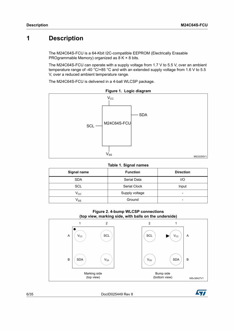
1 Description
The M24C64S-FCU is a 64-Kbit I2C-compatible EEPROM (Electrically Erasable PROgrammable Memory) organized as 8 K × 8 bits.
The M24C64S-FCU can operate with a supply voltage from 1.7 V to 5.5 V, over an ambient temperature range of -40 °C/+85 °C and with an extended supply voltage from 1.6 V to 5.5 V, over a reduced ambient temperature range.
The M24C64S-FCU is delivered in a 4-ball WLCSP package.
Figure 1. Logic diagram
Figure 2. 4-bump WLCSP connections(top view, marking side, with balls on the underside)
Table 1. Signal names
Signal name Function Direction
SDA Serial Data I/O
SCL Serial Clock Input
VCC Supply voltage -
VSS Ground -

DocID025449 Rev 8 7/35
M24C64S-FCU Signal description
34
2 Signal description
2.1 Serial Clock (SCL)
SCL is an input. The signal applied on the SCL input is used to strobe the data available on SDA(in) and to output the data on SDA(out).
2.2 Serial Data (SDA)
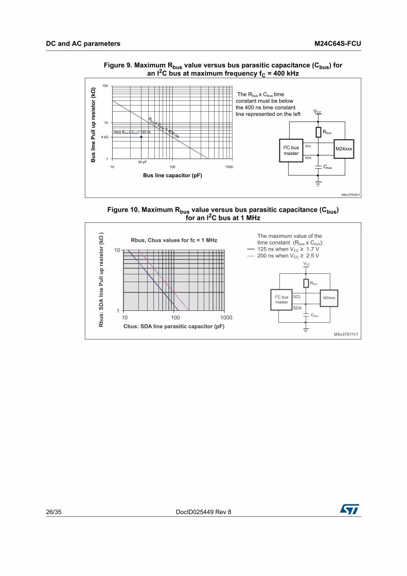
SDA is an input/output used to transfer data in or data out of the device. SDA(out) is an open drain output that may be wire-OR’ed with other open drain or open collector signals on the bus. A pull-up resistor must be connected from Serial Data (SDA) to VCC (Figure 9 indicates how to calculate the value of the pull-up resistor).
2.3 VSS (ground)
VSS is the reference for the VCC supply voltage.
2.4 Supply voltage (VCC)
2.4.1 Operating supply voltage (VCC)
Prior to selecting the memory and issuing instructions to it, a valid and stable VCC voltage within the specified [VCC(min), VCC(max)] range must be applied (see Operating conditions in Section 8: DC and AC parameters). In order to secure a stable DC supply voltage, it is recommended to decouple the VCC line with a suitable capacitor (usually from10 nF to 100 nF) close to the VCC/VSS package pins.
This voltage must remain stable and valid until the end of the transmission of the instruction and, for a write instruction, until the completion of the internal write cycle (tW).
2.4.2 Power-up conditions
The VCC voltage has to rise continuously from 0 V up to the minimum VCC operating voltage (see Operating conditions in Section 8: DC and AC parameters).
2.4.3 Device reset
In order to prevent inadvertent write operations during power-up, a power-on-reset (POR) circuit is included.
At power-up, the device does not respond to any instruction until VCC has reached the internal reset threshold voltage. This threshold is lower than the minimum VCC operating voltage (see Operating conditions in Section 8: DC and AC parameters). When VCC passes over the POR threshold, the device is reset and enters the Standby Power mode; however, the device must not be accessed until VCC reaches a valid and stable DC voltage within the specified [VCC(min), VCC(max)] range (see Operating conditions in Section 8: DC and AC parameters).
Signal description M24C64S-FCU
8/35 DocID025449 Rev 8
In a similar way, during power-down (continuous decrease in VCC), the device must not be accessed when VCC drops below VCC(min). When VCC drops below the power-on-reset threshold voltage, the device stops responding to any instruction sent to it.
2.4.4 Power-down conditions
During power-down (continuous decrease in VCC), the device must be in the Standby Power mode (mode reached after decoding a Stop condition, assuming that there is no internal write cycle in progress).

DocID025449 Rev 8 9/35
M24C64S-FCU Memory organization
34
3 Memory organization
The memory is organized as shown below.
Figure 3. Block diagram

Device operation M24C64S-FCU
10/35 DocID025449 Rev 8
4 Device operation
The device supports the I2C protocol. This is summarized in Figure 4. Any device that sends data on to the bus is defined to be a transmitter, and any device that reads the data to be a receiver. The device that controls the data transfer is known as the bus master, and the other as the slave device. A data transfer can only be initiated by the bus master, which will also provide the serial clock for synchronization. The device is always a slave in all communications.
Figure 4. I2C bus protocol

DocID025449 Rev 8 11/35
M24C64S-FCU Device operation
34
4.1 Start condition
Start is identified by a falling edge of Serial Data (SDA) while Serial Clock (SCL) is stable in the high state. A Start condition must precede any data transfer instruction. The device continuously monitors (except during a Write cycle) Serial Data (SDA) and Serial Clock (SCL) for a Start condition.
4.2 Stop condition
Stop is identified by a rising edge of Serial Data (SDA) while Serial Clock (SCL) is stable and driven high. A Stop condition terminates communication between the device and the bus master. A Read instruction that is followed by NoAck can be followed by a Stop condition to force the device into the Standby mode.
A Stop condition at the end of a Write instruction triggers the internal Write cycle.
4.3 Data input
During data input, the device samples Serial Data (SDA) on the rising edge of Serial Clock (SCL). For correct device operation, Serial Data (SDA) must be stable during the rising edge of Serial Clock (SCL), and the Serial Data (SDA) signal must change only when Serial Clock (SCL) is driven low.
4.4 Acknowledge bit (ACK)
The acknowledge bit is used to indicate a successful byte transfer. The bus transmitter, whether it be bus master or slave device, releases Serial Data (SDA) after sending eight bits of data. During the 9th clock pulse period, the receiver pulls Serial Data (SDA) low to acknowledge the receipt of the eight data bits.
Device operation M24C64S-FCU
12/35 DocID025449 Rev 8
4.5 Device addressing
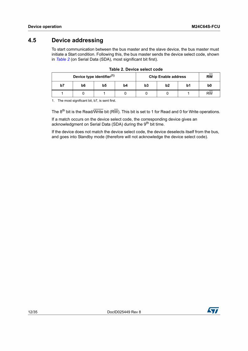
To start communication between the bus master and the slave device, the bus master must initiate a Start condition. Following this, the bus master sends the device select code, shown in Table 2 (on Serial Data (SDA), most significant bit first).
The 8th bit is the Read/Write bit (RW). This bit is set to 1 for Read and 0 for Write operations.
If a match occurs on the device select code, the corresponding device gives an acknowledgment on Serial Data (SDA) during the 9th bit time.
If the device does not match the device select code, the device deselects itself from the bus, and goes into Standby mode (therefore will not acknowledge the device select code).
Table 2. Device select code
Device type identifier(1)
1. The most significant bit, b7, is sent first.
Chip Enable address RW
b7 b6 b5 b4 b3 b2 b1 b0
1 0 1 0 0 0 1 RW

DocID025449 Rev 8 13/35
M24C64S-FCU Instructions
34
5 Instructions
5.1 Write operations
Following a Start condition the bus master sends a device select code with the R/W bit (RW) reset to 0. The device acknowledges this, as shown in Figure 5, and waits for two address bytes. The device responds to each address byte with an acknowledge bit, and then waits for the data byte.
When the bus master generates a Stop condition immediately after a data byte Ack bit (in the “10th bit” time slot), either at the end of a Byte Write or a Page Write, the internal Write cycle tW is triggered. A Stop condition at any other time slot does not trigger the internal Write cycle.
After the Stop condition and the successful completion of an internal Write cycle (tW), the device internal address counter is automatically incremented to point to the next byte after the last modified byte.
During the internal Write cycle, Serial Data (SDA) is disabled internally, and the device does not respond to any requests.
Table 3. Most significant address byte
A15 A14 A13 A12 A11 A10 A9 A8
Table 4. Least significant address byte
A7 A6 A5 A4 A3 A2 A1 A0
Instructions M24C64S-FCU
14/35 DocID025449 Rev 8
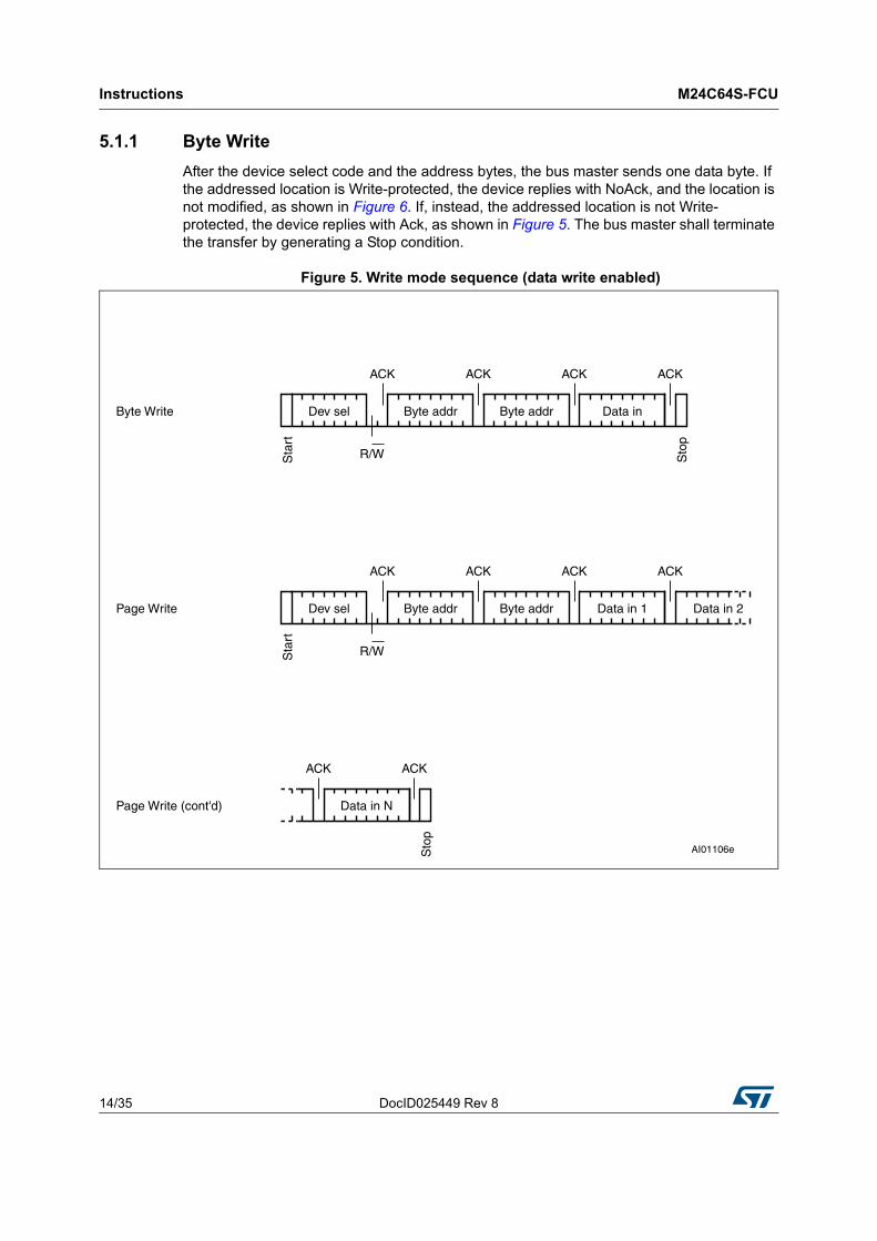
5.1.1 Byte Write
After the device select code and the address bytes, the bus master sends one data byte. If the addressed location is Write-protected, the device replies with NoAck, and the location is not modified, as shown in Figure 6. If, instead, the addressed location is not Write-protected, the device replies with Ack, as shown in Figure 5. The bus master shall terminate the transfer by generating a Stop condition.
Figure 5. Write mode sequence (data write enabled)

DocID025449 Rev 8 15/35
M24C64S-FCU Instructions
34
5.1.2 Page Write
The Page Write mode allows up to 32 bytes to be written in a single Write cycle, provided that they are all located in the same page in the memory: that is, the most significant memory address bits, A15/A5, are the same. If more bytes are sent than will fit up to the end of the page, a “roll-over” occurs, i.e. the bytes exceeding the page end are written on the same page, from location 0.
The bus master sends from 1 to 32 bytes of data, each of which is acknowledged by the device if the page is not write-protected, as shown in Figure 5. If the page is write-protected, the contents of the addressed memory location are not modified, and each data byte is followed by a NoAck, as shown in Figure 6. After each transferred byte, the internal page address counter is incremented.
The transfer is terminated by the bus master generating a Stop condition.
Figure 6. Write mode sequence (data write inhibited)
Sto
p
Sta
rt
Byte Write Dev sel Byte addr Byte addr Data in
Sta
rt
Page Write Dev sel Byte addr Byte addr Data in 1 Data in 2
AI01120e
Page Write (cont'd)
Sto
p
Data in N
ACK ACK ACK NO ACK
R/W
ACK ACK ACK NO ACK
R/W
NO ACK NO ACK
Instructions M24C64S-FCU
16/35 DocID025449 Rev 8
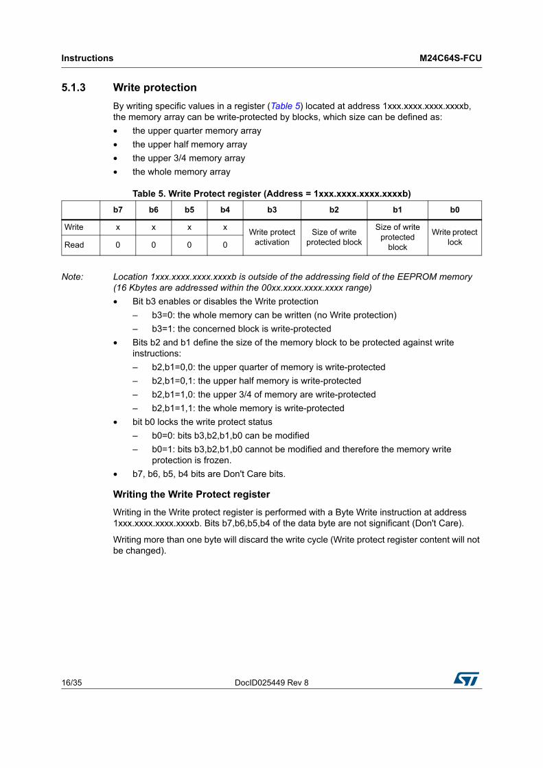
5.1.3 Write protection
By writing specific values in a register (Table 5) located at address 1xxx.xxxx.xxxx.xxxxb, the memory array can be write-protected by blocks, which size can be defined as:
• the upper quarter memory array
• the upper half memory array
• the upper 3/4 memory array
• the whole memory array
Note: Location 1xxx.xxxx.xxxx.xxxxb is outside of the addressing field of the EEPROM memory (16 Kbytes are addressed within the 00xx.xxxx.xxxx.xxxx range)
• Bit b3 enables or disables the Write protection
– b3=0: the whole memory can be written (no Write protection)
– b3=1: the concerned block is write-protected
• Bits b2 and b1 define the size of the memory block to be protected against write instructions:
– b2,b1=0,0: the upper quarter of memory is write-protected
– b2,b1=0,1: the upper half memory is write-protected
– b2,b1=1,0: the upper 3/4 of memory are write-protected
– b2,b1=1,1: the whole memory is write-protected
• bit b0 locks the write protect status
– b0=0: bits b3,b2,b1,b0 can be modified
– b0=1: bits b3,b2,b1,b0 cannot be modified and therefore the memory write protection is frozen.
• b7, b6, b5, b4 bits are Don't Care bits.
Writing the Write Protect register
Writing in the Write protect register is performed with a Byte Write instruction at address 1xxx.xxxx.xxxx.xxxxb. Bits b7,b6,b5,b4 of the data byte are not significant (Don't Care).
Writing more than one byte will discard the write cycle (Write protect register content will not be changed).
Table 5. Write Protect register (Address = 1xxx.xxxx.xxxx.xxxxb)
b7 b6 b5 b4 b3 b2 b1 b0
Write x x x xWrite protect
activationSize of write
protected block
Size of write protected
block
Write protect lockRead 0 0 0 0

DocID025449 Rev 8 17/35
M24C64S-FCU Instructions
34
5.1.4 Minimizing Write delays by polling on ACK
During the internal Write cycle, the device disconnects itself from the bus, and writes a copy of the data from its internal latches to the memory cells. The maximum Write time (tw) is shown in AC characteristics tables in Section 8: DC and AC parameters, but the typical time is shorter. To make use of this, a polling sequence can be used by the bus master.
The sequence, as shown in Figure 7, is:
• Initial condition: a Write cycle is in progress.
• Step 1: the bus master issues a Start condition followed by a device select code (the first byte of the new instruction).
• Step 2: if the device is busy with the internal Write cycle, no Ack will be returned and the bus master goes back to Step 1. If the device has terminated the internal Write cycle, it responds with an Ack, indicating that the device is ready to receive the second part of the instruction (the first byte of this instruction having been sent during Step 1).
Figure 7. Write cycle polling flowchart using ACK
1. The seven most significant bits of the Device Select code of a Random Read (bottom right box in the figure) must be identical to the seven most significant bits of the Device Select code of the Write (polling instruction in the figure).

Instructions M24C64S-FCU
18/35 DocID025449 Rev 8
5.2 Read operations
Read operations are performed independently of the Write protection state.
After the successful completion of a Read operation, the device internal address counter is incremented by one, to point to the next byte address.
For the Read instructions, after each byte read (data out), the device waits for an acknowledgment (data in) during the 9th bit time. If the bus master does not acknowledge during this 9th time, the device terminates the data transfer and switches to its Standby mode.
Figure 8. Read mode sequences
5.2.1 Random Address Read
A dummy Write is first performed to load the address into this address counter (as shown in Figure 8) but without sending a Stop condition. Then, the bus master sends another Start condition, and repeats the device select code, with the RW bit set to 1. The device acknowledges this, and outputs the contents of the addressed byte. The bus master must not acknowledge the byte, and terminates the transfer with a Stop condition.

DocID025449 Rev 8 19/35
M24C64S-FCU Instructions
34
5.2.2 Current Address Read
For the Current Address Read operation, following a Start condition, the bus master only sends a device select code with the R/W bit set to 1. The device acknowledges this, and outputs the byte addressed by the internal address counter. The counter is then incremented. The bus master terminates the transfer with a Stop condition, as shown in Figure 8, without acknowledging the byte.
5.2.3 Sequential Read
This operation can be used after a Current Address Read or a Random Address Read. The bus master does acknowledge the data byte output, and sends additional clock pulses so that the device continues to output the next byte in sequence. To terminate the stream of bytes, the bus master must not acknowledge the last byte, and must generate a Stop condition, as shown in Figure 8.
The output data comes from consecutive addresses, with the internal address counter automatically incremented after each byte output. After the last memory address, the address counter “rolls-over”, and the device continues to output data from memory address 00h.
5.2.4 Read the Write Protect register
Reading the Write Protect register is performed with a Random Read instruction at address 1xxx.xxxx.xxxx.xxxxb. Bits b7, b6, b5, b4 of the Write Protect register content are read as 0, 0, 0, 0. The signification of the Protect Register lower bits b3, b2, b1, b0 are defined in Section 5.1.3: Write protection.
Reading more than one byte will loop on reading the Write Protect Register value.
The Write Protect register cannot be read while a write cycle (tw) is ongoing.

Initial delivery state M24C64S-FCU
20/35 DocID025449 Rev 8
6 Initial delivery state
The device is delivered with all the memory array bits set to 1 (each byte contains FFh) and the Write Protect register set to 0 (00h).
DocID025449 Rev 8 21/35
M24C64S-FCU Maximum rating
34
7 Maximum rating
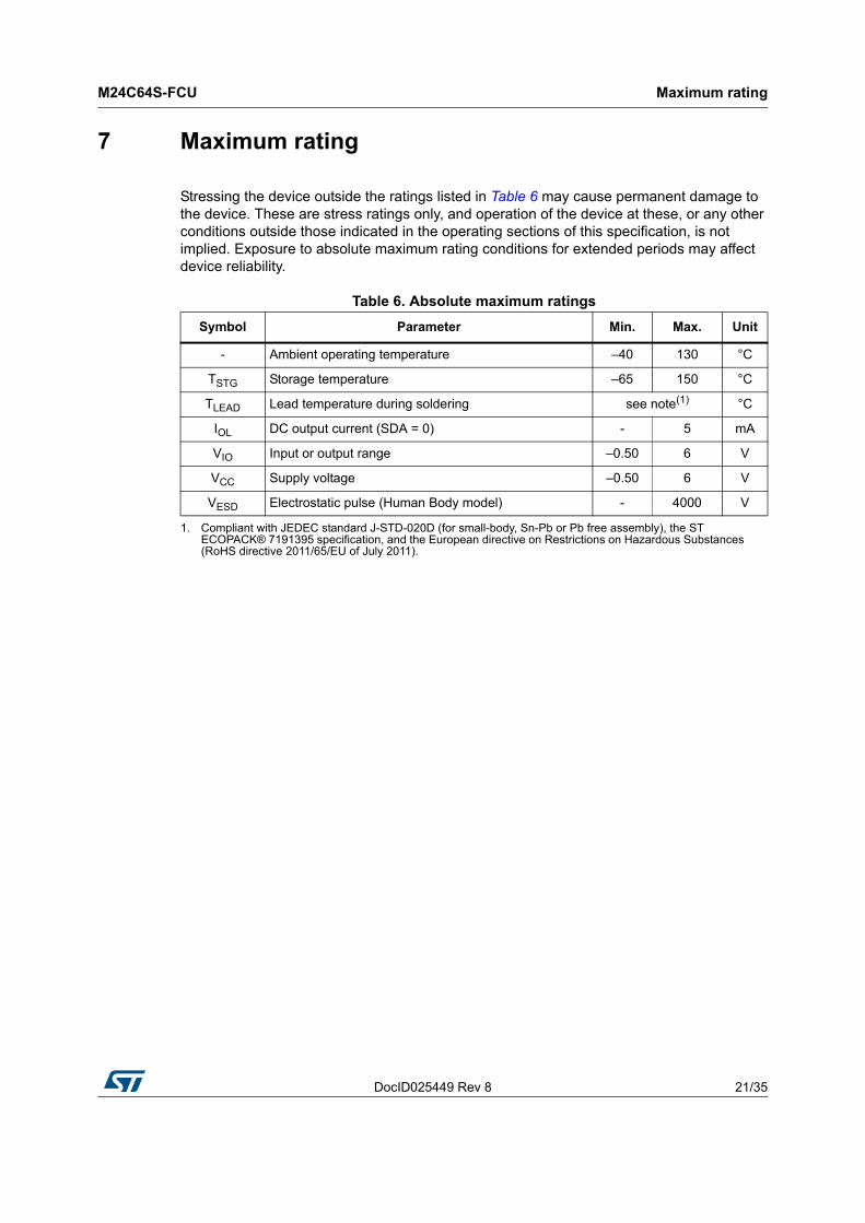
Stressing the device outside the ratings listed in Table 6 may cause permanent damage to the device. These are stress ratings only, and operation of the device at these, or any other conditions outside those indicated in the operating sections of this specification, is not implied. Exposure to absolute maximum rating conditions for extended periods may affect device reliability.
Table 6. Absolute maximum ratings
Symbol Parameter Min. Max. Unit
- Ambient operating temperature –40 130 °C
TSTG Storage temperature –65 150 °C
TLEAD Lead temperature during soldering see note(1)
1. Compliant with JEDEC standard J-STD-020D (for small-body, Sn-Pb or Pb free assembly), the ST ECOPACK® 7191395 specification, and the European directive on Restrictions on Hazardous Substances (RoHS directive 2011/65/EU of July 2011).
°C
IOL DC output current (SDA = 0) - 5 mA
VIO Input or output range –0.50 6 V
VCC Supply voltage –0.50 6 V
VESD Electrostatic pulse (Human Body model) - 4000 V
DC and AC parameters M24C64S-FCU
22/35 DocID025449 Rev 8
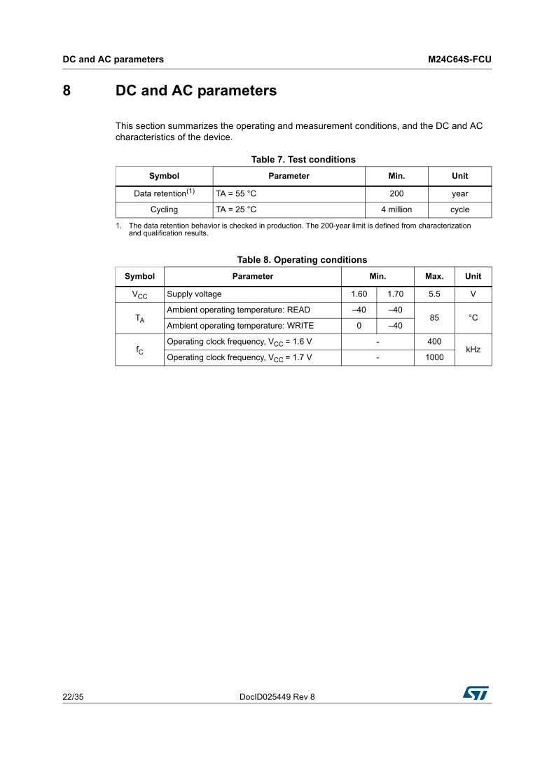
8 DC and AC parameters
This section summarizes the operating and measurement conditions, and the DC and AC characteristics of the device.
Table 7. Test conditions
Symbol Parameter Min. Unit
Data retention(1)
1. The data retention behavior is checked in production. The 200-year limit is defined from characterization and qualification results.
TA = 55 °C 200 year
Cycling TA = 25 °C 4 million cycle
Table 8. Operating conditions
Symbol Parameter Min. Max. Unit
VCC Supply voltage 1.60 1.70 5.5 V
TA
Ambient operating temperature: READ –40 –4085 °C
Ambient operating temperature: WRITE 0 –40
fCOperating clock frequency, VCC = 1.6 V - 400
kHzOperating clock frequency, VCC = 1.7 V - 1000

DocID025449 Rev 8 23/35
M24C64S-FCU DC and AC parameters
34
Table 9. DC characteristics
Symbol Parameter Test conditions Min. Max. Unit
ILIInput leakage current (SCL, SDA)
VIN = VSS or VCC device in Standby mode
- ± 2 µA
ILOOutput leakage current
SDA in Hi-Z, external voltage applied on SDA: VSS or VCC
- ± 2 µA
ICC Supply current (Read)
VCC < 1.8 V, fC = 400 kHz - 0.8 mA
VCC >= 1.8 V, fC = 400 kHz - 2 mA
VCC >= 1.8 V, fC = 1 MHz(1)
1. Only for devices operating at fcMax = 1 MHz (See Table 8)
- 2.5 mA
ICC0Supply current (Write)(2)
2. Characterized value, not tested in production.
During tW - 2 mA
ICC1Standby supply current
Device not selected (3), VIN = VSS or VCC, VCC = 1.8 V
3. The device is not selected after power-up, after a Read instruction (after the Stop condition), or after the completion of the internal write cycle tW (tW is triggered by the correct decoding of a Write instruction).
- 1 µA
Device not selected (3), VIN = VSS or VCC, VCC = 2.5 V
- 2 µA
Device not selected (3), VIN = VSS or VCC, VCC = 5.5 V
- 3 µA
VILInput low voltage (SCL, SDA)
- –0.45 0.25 VCC V
VIHInput high voltage (SCL, SDA)
- 0.75 VCC VCC + 1 V
VOL Output low voltage
IOL = 1 mA, VCC < 1.8 V - 0.2 V
IOL = 2.1 mA, VCC = 2.5 V - 0.4 V
IOL = 3 mA, VCC = 5.5 V - 0.4 V
DC and AC parameters M24C64S-FCU
24/35 DocID025449 Rev 8
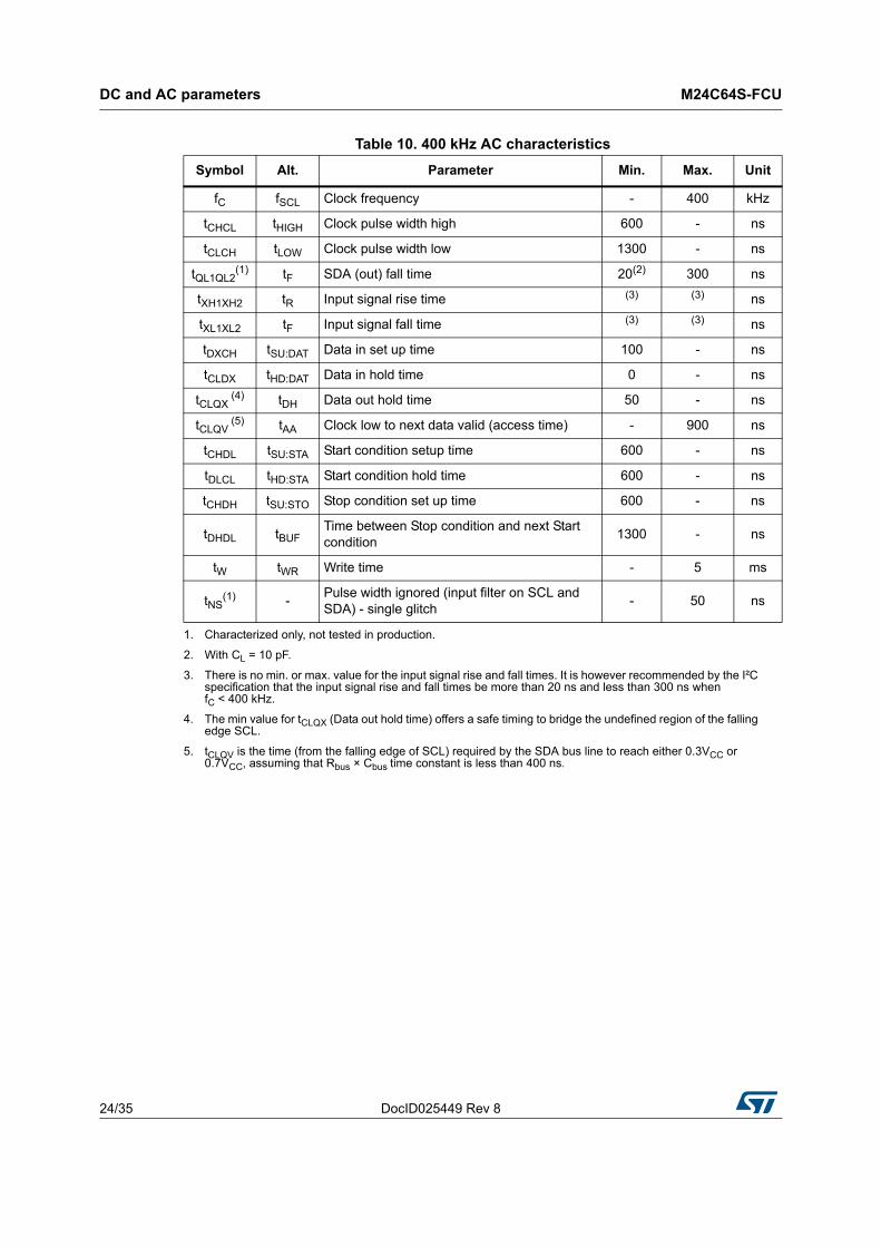
Table 10. 400 kHz AC characteristics
Symbol Alt. Parameter Min. Max. Unit
fC fSCL Clock frequency - 400 kHz
tCHCL tHIGH Clock pulse width high 600 - ns
tCLCH tLOW Clock pulse width low 1300 - ns
tQL1QL2(1)
1. Characterized only, not tested in production.
tF SDA (out) fall time 20(2)
2. With CL = 10 pF.
300 ns
tXH1XH2 tR Input signal rise time (3)
3. There is no min. or max. value for the input signal rise and fall times. It is however recommended by the I²C specification that the input signal rise and fall times be more than 20 ns and less than 300 ns when fC < 400 kHz.
(3) ns
tXL1XL2 tF Input signal fall time (3) (3) ns
tDXCH tSU:DAT Data in set up time 100 - ns
tCLDX tHD:DAT Data in hold time 0 - ns
tCLQX (4)
4. The min value for tCLQX (Data out hold time) offers a safe timing to bridge the undefined region of the falling edge SCL.
tDH Data out hold time 50 - ns
tCLQV (5)
5. tCLQV is the time (from the falling edge of SCL) required by the SDA bus line to reach either 0.3VCC or 0.7VCC, assuming that Rbus × Cbus time constant is less than 400 ns.
tAA Clock low to next data valid (access time) - 900 ns
tCHDL tSU:STA Start condition setup time 600 - ns
tDLCL tHD:STA Start condition hold time 600 - ns
tCHDH tSU:STO Stop condition set up time 600 - ns
tDHDL tBUFTime between Stop condition and next Start condition
1300 - ns
tW tWR Write time - 5 ms
tNS(1) -
Pulse width ignored (input filter on SCL and SDA) - single glitch
- 50 ns
DocID025449 Rev 8 25/35
M24C64S-FCU DC and AC parameters
34
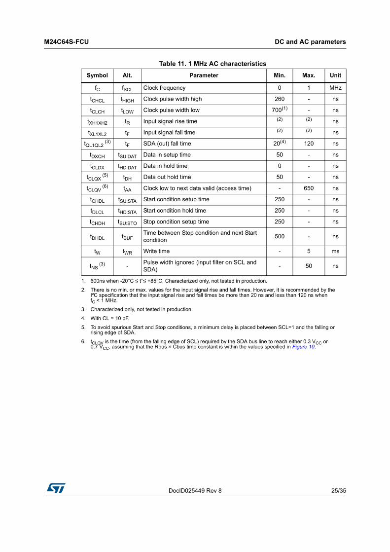
Table 11. 1 MHz AC characteristics
Symbol Alt. Parameter Min. Max. Unit
fC fSCL Clock frequency 0 1 MHz
tCHCL tHIGH Clock pulse width high 260 - ns
tCLCH tLOW Clock pulse width low 700(1)
1. 600ns when -20°C ≤ t°≤ +85°C. Characterized only, not tested in production.
- ns
tXH1XH2 tR Input signal rise time (2)
2. There is no min. or max. values for the input signal rise and fall times. However, it is recommended by the I²C specification that the input signal rise and fall times be more than 20 ns and less than 120 ns when fC < 1 MHz.
(2) ns
tXL1XL2 tF Input signal fall time (2) (2) ns
tQL1QL2 (3)
3. Characterized only, not tested in production.
tF SDA (out) fall time 20(4)
4. With CL = 10 pF.
120 ns
tDXCH tSU:DAT Data in setup time 50 - ns
tCLDX tHD:DAT Data in hold time 0 - ns
tCLQX (5)
5. To avoid spurious Start and Stop conditions, a minimum delay is placed between SCL=1 and the falling or rising edge of SDA.
tDH Data out hold time 50 - ns
tCLQV (6)
6. tCLQV is the time (from the falling edge of SCL) required by the SDA bus line to reach either 0.3 VCC or 0.7 VCC, assuming that the Rbus × Cbus time constant is within the values specified in Figure 10.
tAA Clock low to next data valid (access time) - 650 ns
tCHDL tSU:STA Start condition setup time 250 - ns
tDLCL tHD:STA Start condition hold time 250 - ns
tCHDH tSU:STO Stop condition setup time 250 - ns
tDHDL tBUFTime between Stop condition and next Start condition
500 - ns
tW tWR Write time - 5 ms
tNS (3) -
Pulse width ignored (input filter on SCL and SDA)
- 50 ns
DC and AC parameters M24C64S-FCU
26/35 DocID025449 Rev 8
Figure 9. Maximum Rbus value versus bus parasitic capacitance (Cbus) foran I2C bus at maximum frequency fC = 400 kHz
Figure 10. Maximum Rbus value versus bus parasitic capacitance (Cbus) for an I2C bus at 1 MHz

DocID025449 Rev 8 27/35
M24C64S-FCU DC and AC parameters
34
Figure 11. AC waveforms
Package information M24C64S-FCU
28/35 DocID025449 Rev 8
9 Package information
In order to meet environmental requirements, ST offers these devices in different grades of ECOPACK® packages, depending on their level of environmental compliance. ECOPACK® specifications, grade definitions and product status are available at: www.st.com. ECOPACK® is an ST trademark.
9.1 Ultra Thin WLCSP package information
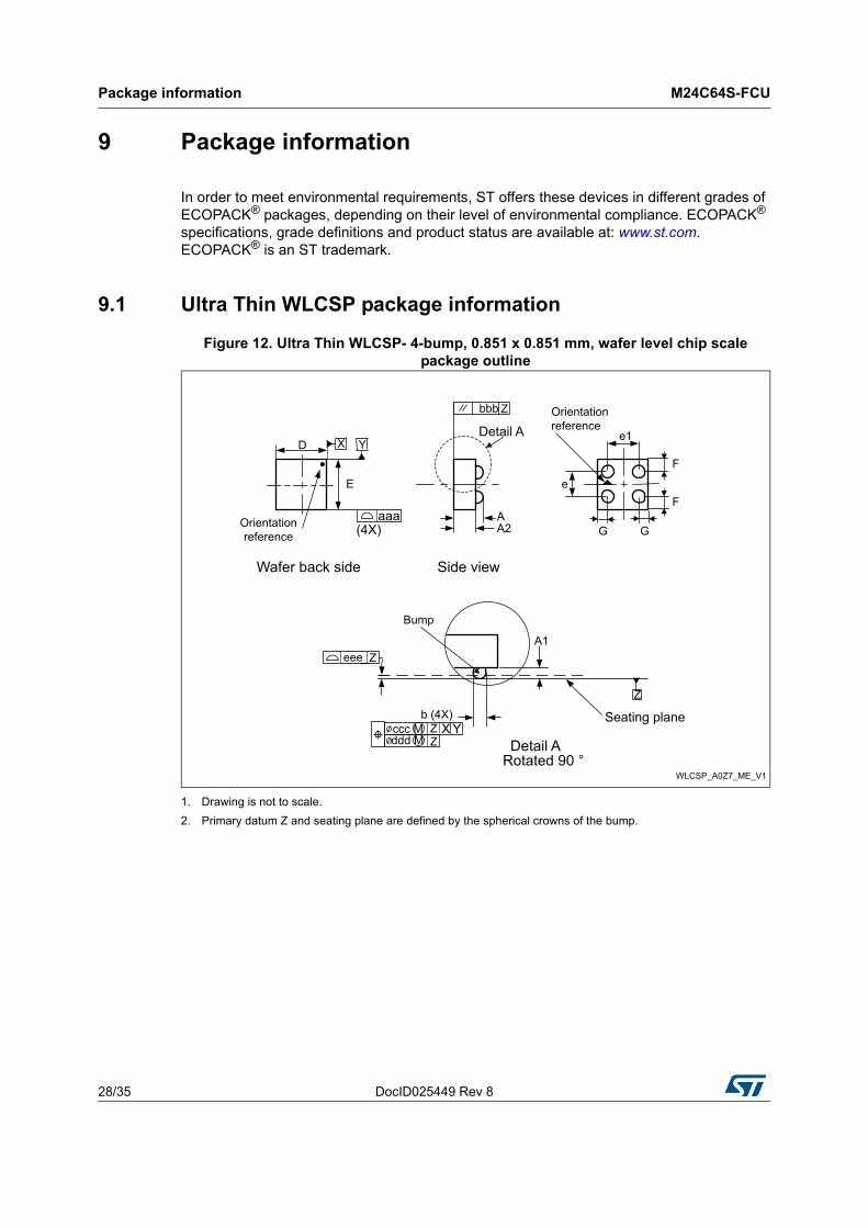
Figure 12. Ultra Thin WLCSP- 4-bump, 0.851 x 0.851 mm, wafer level chip scale package outline
1. Drawing is not to scale.
2. Primary datum Z and seating plane are defined by the spherical crowns of the bump.

DocID025449 Rev 8 29/35
M24C64S-FCU Package information
34
Table 12. Ultra Thin WLCSP- 4-bump, 0.851 x 0.851 mm, wafer level chip scale package mechanical data
Symbolmillimeters inches(1)
1. Values in inches are converted from mm and rounded to 4 decimal digits.
Min Typ Max Min Typ Max
A 0.240 0.270 0.300 0.0094 0.0106 0.0118
A1 - 0.095 - - 0.0037 -
A2 - 0.175 - - 0.0069 -
b(2) (3)
2. Dimension is measured at the maximum bump diameter parallel to primary datum Z.
3. Primary datum Z and seating plane are defined by the spherical crowns of the bump.
- 0.185 - - 0.0073 -
D - 0.851 0.871 - 0.0335 0.0343
E - 0.851 0.871 - 0.0335 0.0343
e - 0.400 - - 0.0157 -
e1 0.500 0.0197
F - 0.226 - - 0.0089 -
G - 0.176 - - 0.0069 -
aaa - 0.110 - - 0.0043 -
bbb - 0.110 - - 0.0043 -
ccc - 0.110 - - 0.0043 -
ddd - 0.060 - - 0.0024 -
eee - 0.060 - - 0.0024 -
Package information M24C64S-FCU
30/35 DocID025449 Rev 8
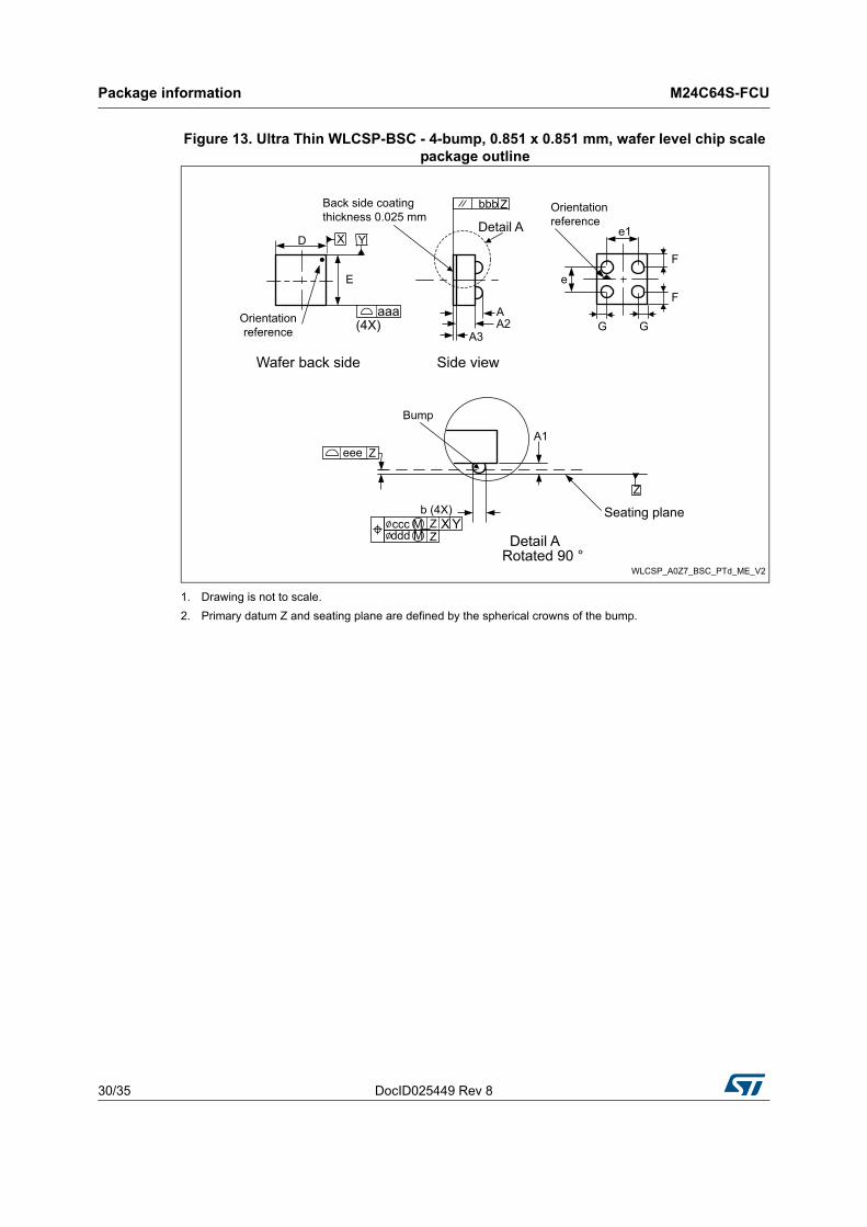
Figure 13. Ultra Thin WLCSP-BSC - 4-bump, 0.851 x 0.851 mm, wafer level chip scale package outline
1. Drawing is not to scale.
2. Primary datum Z and seating plane are defined by the spherical crowns of the bump.
DocID025449 Rev 8 31/35
M24C64S-FCU Package information
34
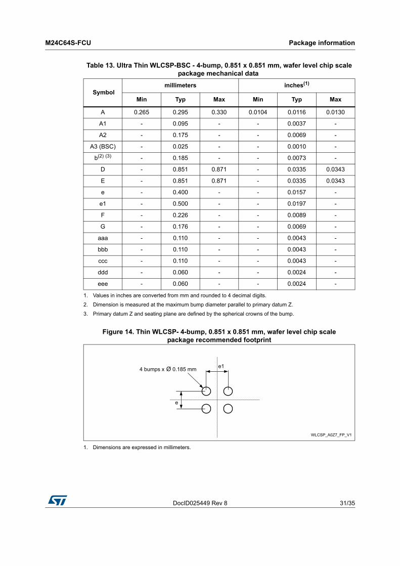
Figure 14. Thin WLCSP- 4-bump, 0.851 x 0.851 mm, wafer level chip scale package recommended footprint
1. Dimensions are expressed in millimeters.
Table 13. Ultra Thin WLCSP-BSC - 4-bump, 0.851 x 0.851 mm, wafer level chip scale package mechanical data
Symbolmillimeters inches(1)
1. Values in inches are converted from mm and rounded to 4 decimal digits.
Min Typ Max Min Typ Max
A 0.265 0.295 0.330 0.0104 0.0116 0.0130
A1 - 0.095 - - 0.0037 -
A2 - 0.175 - - 0.0069 -
A3 (BSC) - 0.025 - - 0.0010 -
b(2) (3)
2. Dimension is measured at the maximum bump diameter parallel to primary datum Z.
3. Primary datum Z and seating plane are defined by the spherical crowns of the bump.
- 0.185 - - 0.0073 -
D - 0.851 0.871 - 0.0335 0.0343
E - 0.851 0.871 - 0.0335 0.0343
e - 0.400 - - 0.0157 -
e1 - 0.500 - - 0.0197 -
F - 0.226 - - 0.0089 -
G - 0.176 - - 0.0069 -
aaa - 0.110 - - 0.0043 -
bbb - 0.110 - - 0.0043 -
ccc - 0.110 - - 0.0043 -
ddd - 0.060 - - 0.0024 -
eee - 0.060 - - 0.0024 -
Part numbering M24C64S-FCU
32/35 DocID025449 Rev 8
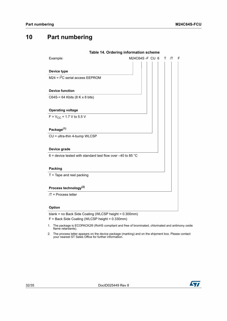
10 Part numbering
Table 14. Ordering information scheme
Example: M24C64S -F CU 6 T /T F
Device type
M24 = I2C serial access EEPROM
Device function
C64S = 64 Kbits (8 K x 8 bits)
Operating voltage
F = VCC = 1.7 V to 5.5 V
Package(1)
1. The package is ECOPACK2® (RoHS compliant and free of brominated, chlorinated and antimony oxide flame retardants).
CU = ultra-thin 4-bump WLCSP
Device grade
6 = device tested with standard test flow over –40 to 85 °C
Packing
T = Tape and reel packing
Process technology(2)
2. The process letter appears on the device package (marking) and on the shipment box. Please contact your nearest ST Sales Office for further information.
/T = Process letter
Option
blank = no Back Side Coating (WLCSP height = 0.300mm)
F = Back Side Coating (WLCSP height = 0.330mm)
DocID025449 Rev 8 33/35
M24C64S-FCU Part numbering
34
Engineering samples
Parts marked as “ES”, “E” or accompanied by an Engineering Sample notification letter, are not yet qualified and therefore not yet ready to be used in production and any consequences deriving from such usage will not be at ST charge. In no event, ST will be liable for any customer usage of these engineering samples in production. ST Quality has to be contacted prior to any decision to use these Engineering samples to run qualification activity.

Revision history M24C64S-FCU
34/35 DocID025449 Rev 8
11 Revision history
Table 15. Document revision history
Date Revision Changes
06-Dec-2013 1 Initial release.
21-Mar-2014 2
Updated Supply voltage and Operating temperature ranges in Features
Updated Section 1: Description
Updated Table 8: Operating conditions
30-May-2014 3Added Figure 12: Ultra Thin WLCSP- 4-bump, 0.833 x 0.833 mm, wafer level chip scale package outline.
04-Dec-2014 4
Updated Features
Updated Table 8: Operating conditions
Added Figure 10: Maximum Rbus value versus bus parasitic capacitance (Cbus) for an I2C bus at high clock frequency
Added Figure 12: Ultra Thin WLCSP- 4-bump, 0.833 x 0.833 mm, wafer level chip scale package outline
Added Figure 13: Ultra Thin WLCSP- 4-bump, 0.833 x 0.833 mm, wafer level chip scale package outline with BSC
Added Figure 14: Thin WLCSP- 4-bump, 0.833 x 0.833 mm, wafer level chip scale package recommended footprint
Added Table 11: 1 MHz AC characteristics.
Updated Table 12: Ultra Thin WLCSP- 4-bump, 0.833 x 0.833 mm, wafer level chip scale package mechanical data
Added Table 13: Ultra Thin WLCSP- 4-bump, 0.833 x 0.833 mm, wafer level chip scale package mechanical data
Added option F inside Table 14: Ordering information scheme
28-Apr-2015 5
Change from Preliminary to Production data status
Updated Icc(read) value in Table 9: DC characteristics
Updated Figure 31: Maximum Rbus value versus bus parasitic capacitance (Cbus) for an I2C bus at high clock frequency
26-Aug-2015 6
Updated:
– data retention and write cycles on cover page.
– Figure 2
– Table 7
14-Oct-2015 7
Added:
– Note 1 on Table 11.
– Notes 1 and 2 on Table 14
29-Jun-2016 8
updated: Section 2.4.2: Power-up conditions, tTable 12: Ultra Thin WLCSP- 4-bump, 0.851 x 0.851 mm, wafer level chip scale package mechanical data, Table 7: Test conditions, Figure 13: Ultra Thin WLCSP-BSC - 4-bump, 0.851 x 0.851 mm, wafer level chip scale package outline
DocID025449 Rev 8 35/35
M24C64S-FCU
35
IMPORTANT NOTICE – PLEASE READ CAREFULLY
STMicroelectronics NV and its subsidiaries (“ST”) reserve the right to make changes, corrections, enhancements, modifications, and improvements to ST products and/or to this document at any time without notice. Purchasers should obtain the latest relevant information on ST products before placing orders. ST products are sold pursuant to ST’s terms and conditions of sale in place at the time of order acknowledgement.
Purchasers are solely responsible for the choice, selection, and use of ST products and ST assumes no liability for application assistance or the design of Purchasers’ products.
No license, express or implied, to any intellectual property right is granted by ST herein.
Resale of ST products with provisions different from the information set forth herein shall void any warranty granted by ST for such product.
ST and the ST logo are trademarks of ST. All other product or service names are the property of their respective owners.
Information in this document supersedes and replaces information previously supplied in any prior versions of this document.
© 2016 STMicroelectronics – All rights reserved