Embed Size (px)
Citation preview
628 IEEE TRANSACTIONS ON VERY LARGE SCALE INTEGRATION (VLSI) SYSTEMS, VOL. 16, NO. 6, JUNE 2008
L-CBF: A Low-Power, Fast CountingBloom Filter Architecture
Elham Safi, Student Member, IEEE, Andreas Moshovos, Senior Member, IEEE, andAndreas Veneris, Senior Member, IEEE
Abstract—An increasing number of architectural techniqueshave relied on hardware counting bloom filters (CBFs) to improveupon the energy, delay, and complexity of various processor struc-tures. CBFs improve the energy and speed of membership tests bymaintaining an imprecise and compact representation of a largeset to be searched. This paper studies the energy, delay, and areacharacteristics of two implementations for CBFs using full customlayouts in a commercial 0.13- m fabrication technology. One im-plementation, S-CBF, uses an SRAM array of counts and a sharedup/down counter. Our proposed implementation, L-CBF, utilizesan array of up/down linear feedback shift registers and local zerodetectors. Circuit simulations show that for a 1 K-entry CBF witha 15-bit count per entry, L-CBF compared to S-CBF is 3.7 or1.6 faster and requires 2.3 or 1.4 less energy depending onthe operation. Additionally, this paper presents analytical energyand delay models for L-CBF. These models can estimate energyand delay of various CBF organizations during architectural levelexplorations when a physical level implementation is not available.Our results demonstrate that for a variety of L-CBF organizations,the estimations by analytical models are within 5% and 10% ofSpectre simulation results for delay and energy, respectively.
Index Terms—Computer architecture, counting bloom filters,implementation, low power, microprocessors.
I. INTRODUCTION
A N increasing number of architectural techniques have re-lied on hardware counting bloom filters (CBFs) to im-
prove upon the power, delay, and complexity of various pro-cessor structures. For example, CBFs have been used to im-prove performance and power in snoop-coherent multiprocessoror multi-core systems [1], [2]. CBFs have been also utilized toimprove the scalability of load/store scheduling queues [3] andto reduce instruction replays by assisting in early miss determi-nation at the L1 data cache [4]. In these applications, CBFs helpeliminate broadcasts over the interconnection network in multi-processor systems [1]; CBFs also help reduce accesses to muchlarger and thus much slower and power-hungry content address-able memories [3], or cache tag arrays [1], [2], [4].
In all aforementioned hardware applications, CBFs improvethe energy and speed of membership tests. Checking whether a
Manuscript received February 1, 2007; revised June 18, 2007. This work wassupported in part by an NSERC Discovery Grant, by a Canada Foundation forInnovation Equipment Grant, and by funds from the University of Toronto. Thispaper appeared in part in the Proceedings of the 2006 International Symposiumon Low Power Electronics Design, Tegernsee, Bavaria, Germany, October 4–6,2006, pp. 250–255.
The authors are with the Department of Electrical and Computer Engineering,University of Toronto, Toronto, ON M5S 3G4 Canada (e-mail: [email protected]; [email protected]; [email protected]).
Digital Object Identifier 10.1109/TVLSI.2008.2000244
memory block is currently cached is an example of a member-ship test in processors [4]. The CBF provides a definite answerfor most, but not necessarily for all, membership tests. As such,the CBF does not replace entirely the underlying conventionalmechanism (e.g., cache tags), but it dynamically bypasses theconventional mechanism, which can be slow and power hungry,as frequently as possible. Accordingly, the benefits obtainedthrough the use of CBFs depend on two factors. The first factoris how frequently a CBF can be utilized. Architectural tech-niques and application behavior determine how many member-ship tests can be serviced by the CBF. The second factor is theenergy and delay characteristics of the CBF. The more member-ship tests are serviced by the CBF “alone” and the more speedand energy efficient the CBF implementation is, the higher thebenefits.
This work focuses exclusively on the second factor as it in-vestigates implementations of a CBF that improve its energy anddelay characteristics. A key contribution of this work is the in-troduction of L-CBF. L-CBF is an energy- and delay-efficientimplementation that utilizes an array of up/down linear feed-back shift registers (LFSRs) and local zero detectors. Previouswork assumes a straightforward SRAM-based implementationthat we will refer to it as S-CBF [2]. We investigate the en-ergy, delay, and area characteristics of L-CBF and S-CBF im-plementations in a commercial 0.13- m CMOS technology. Wedemonstrate that depending on the type of operation, L-CBFcompared to S-CBF is 3.7 or 1.6 faster and requires 2.3or 1.4 less energy. This work also presents analytical energyand delay models for L-CBF. These analytical models can es-timate energy and delay of various CBF organizations early inthe design stage during architectural level explorations. Theseexplorations are performed well before the physical level im-plementation phase in a design flow. Comparisons show that theestimations by the models are within 5% and 10% of Spectre cir-cuit simulation results for delay and energy, respectively.
The significant contributions of this work are as follows.1) It proposes L-CBF, a novel, energy- and speed-efficientimplementation for CBFs. 2) It compares the energy, delay, andarea of two CBF implementations, L-CBF and S-CBF, usingtheir circuit-level implementations and full-custom layoutsin 0.13- m fabrication technology. 3) It presents analyticaldelay and energy models for L-CBF and compares the modelestimations against simulation results.
The rest of this paper is organized as follows. Section IIreviews CBFs and their previously assumed implementation,S-CBF. Section III-B presents L-CBF, our novel implemen-tation. Section IV discusses the analytical delay and energy
1063-8210/$25.00 © 2008 IEEE
SAFI et al.: L-CBF: A LOW-POWER, FAST COUNTING BLOOM FILTER ARCHITECTURE 629
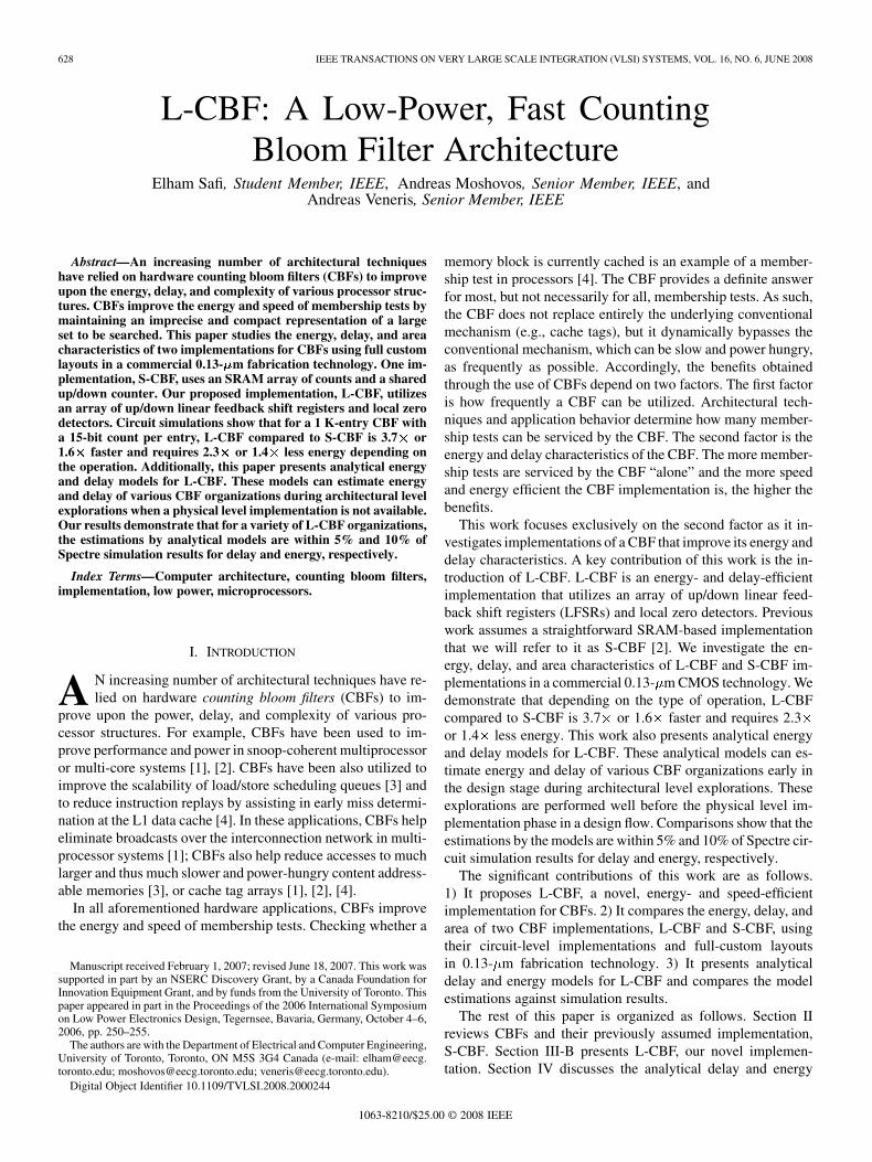
Fig. 1. CBF as a black box.
models of L-CBF. Section V presents the experimental results.Section VI summarizes our findings.
II. CBFS
This section reviews CBFs and their characteristics. Addi-tionally, it discusses the previously assumed implementation forthe CBFs, which has not been investigated at the physical level.
A. Introduction to CBFs
1) CBF as a Black Box: As shown in Fig. 1, a CBF is con-ceptually an array of counts indexed via a hash function ofthe element under membership test. A CBF has three opera-tions: 1) increment count (INC); 2) decrement count (DEC); and3) test if the count is zero (PROBE). The first two operations in-crement or decrement the corresponding count by one, and thethird one checks if the count is zero and returns true or false(single-bit output). We will refer to the first two operations asupdates and to the third one as a probe. A CBF is characterizedby its number of entries and the width of the count per entry.
2) CBF Characteristics: Membership tests using CBFs areperformed by probe operations. In response to a membershiptest, a CBF provides one of the following two answers: 1) “def-inite no,” indicating that the element is definitely not a memberof the large set and 2) “I don’t know,” implying that the CBFcannot assist in a membership test, and the large set must besearched.
The CBF is capable of producing the desired answer to amembership test much faster and saves power on two condi-tions. First, accessing the CBF is significantly faster and re-quires much less energy than accessing the large set. Second,most membership tests are serviced by the CBF. The later is in-vestigated by studying the application behavior. For instance,when CBF is exploited as a miss predictor, previous work [4]shows that more than 95% of the accesses to the cache tag arrayare serviced by the CBF.
The CBF uses an imprecise representation of the large set tobe searched. Ideally, in the CBF, a separate entry would exist forevery element of the set. In this case, the CBF would be capableof precisely representing any set. However, this would require aprohibitively large array negating any benefits. In practice, theCBF is a small array and the element addresses are hashed ontothis small array. Because of hashing, multiple addresses maymap onto the same array entry. Hence, the CBF constitutes animprecise representation of the content of the large set and keepsa superset of the existing elements. This impreciseness is thereason of the “I don’t know” answers by the CBF. To reducethe frequency of such answers, and hence improving accuracy,multiple CBFs with different hash functions can be used.
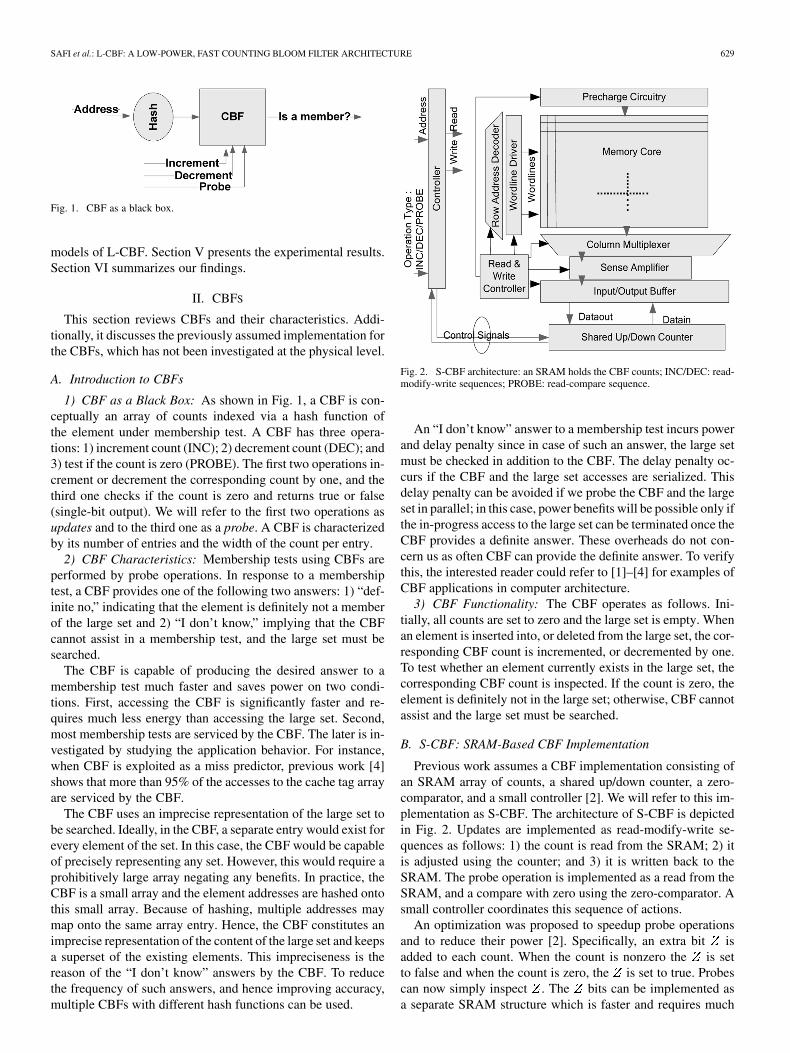
Fig. 2. S-CBF architecture: an SRAM holds the CBF counts; INC/DEC: read-modify-write sequences; PROBE: read-compare sequence.
An “I don’t know” answer to a membership test incurs powerand delay penalty since in case of such an answer, the large setmust be checked in addition to the CBF. The delay penalty oc-curs if the CBF and the large set accesses are serialized. Thisdelay penalty can be avoided if we probe the CBF and the largeset in parallel; in this case, power benefits will be possible only ifthe in-progress access to the large set can be terminated once theCBF provides a definite answer. These overheads do not con-cern us as often CBF can provide the definite answer. To verifythis, the interested reader could refer to [1]–[4] for examples ofCBF applications in computer architecture.
3) CBF Functionality: The CBF operates as follows. Ini-tially, all counts are set to zero and the large set is empty. Whenan element is inserted into, or deleted from the large set, the cor-responding CBF count is incremented, or decremented by one.To test whether an element currently exists in the large set, thecorresponding CBF count is inspected. If the count is zero, theelement is definitely not in the large set; otherwise, CBF cannotassist and the large set must be searched.
B. S-CBF: SRAM-Based CBF Implementation
Previous work assumes a CBF implementation consisting ofan SRAM array of counts, a shared up/down counter, a zero-comparator, and a small controller [2]. We will refer to this im-plementation as S-CBF. The architecture of S-CBF is depictedin Fig. 2. Updates are implemented as read-modify-write se-quences as follows: 1) the count is read from the SRAM; 2) itis adjusted using the counter; and 3) it is written back to theSRAM. The probe operation is implemented as a read from theSRAM, and a compare with zero using the zero-comparator. Asmall controller coordinates this sequence of actions.
An optimization was proposed to speedup probe operationsand to reduce their power [2]. Specifically, an extra bit isadded to each count. When the count is nonzero the is setto false and when the count is zero, the is set to true. Probescan now simply inspect . The bits can be implemented asa separate SRAM structure which is faster and requires much
630 IEEE TRANSACTIONS ON VERY LARGE SCALE INTEGRATION (VLSI) SYSTEMS, VOL. 16, NO. 6, JUNE 2008
less power. This type of optimization is compatible with bothS-CBF and L-CBF architectures.
III. L-CBF: A NOVEL LFSR-BASED CBF IMPLEMENTATION
Section V demonstrates quantitatively that much of theenergy in S-CBF is consumed on the SRAM’s bitlines andwordlines. Additionally, in S-CBF, both delay and energysuffer as updates require two SRAM accesses per operation.The shared counter may increase the energy and the delay fur-ther. We could avoid accesses over long bitlines by building anarray of up/down counters with local zero detectors. In this way,CBF operations would be localized and there would be no needto read/write values over long bitlines. L-CBF is such a design.For the CBF, the actual count values are not important andwe only care whether a count is “zero” or “nonzero.” Hence,any counter that provides a deterministic up/down sequencecan be a choice of counter for the CBF. L-CBF consists of anarray of up/down LFSRs with embedded zero detectors. L-CBFemploys up/down LFSRs that offer a better delay, power, andcomplexity tradeoff than other synchronous up/down counterswith the same count sequence length (see Section III-A2).
As Section V demonstrates, L-CBF significantly reduces en-ergy and delay compared to S-CBF at the cost of more area. Theincrease in area though is a minor concern in modern processordesigns given the abundance of on-chip resources and the verysmall area of the CBF compared to most other processor struc-tures (e.g., caches and branch predictors).
The rest of this section reviews up/down (reversible) LFSRsand discusses the architecture of L-CBF.
A. LFSRs
A maximum-length -bit LFSR sequences throughstates. It goes through all possible code permutations exceptone. The LFSR consists of a shift register and a few embeddedXNOR gates fed by a feedback loop. Each LFSR has the fol-lowing defining parameters:
• width, or size, of the LFSR (it is equal to the number of bitsin the shift register);
• number and positions of taps (taps are special locations inthe LFSR that have a connection with the feedback loop);
• initial state of the LFSR which can be any value except one(all ones for XNOR feedback).
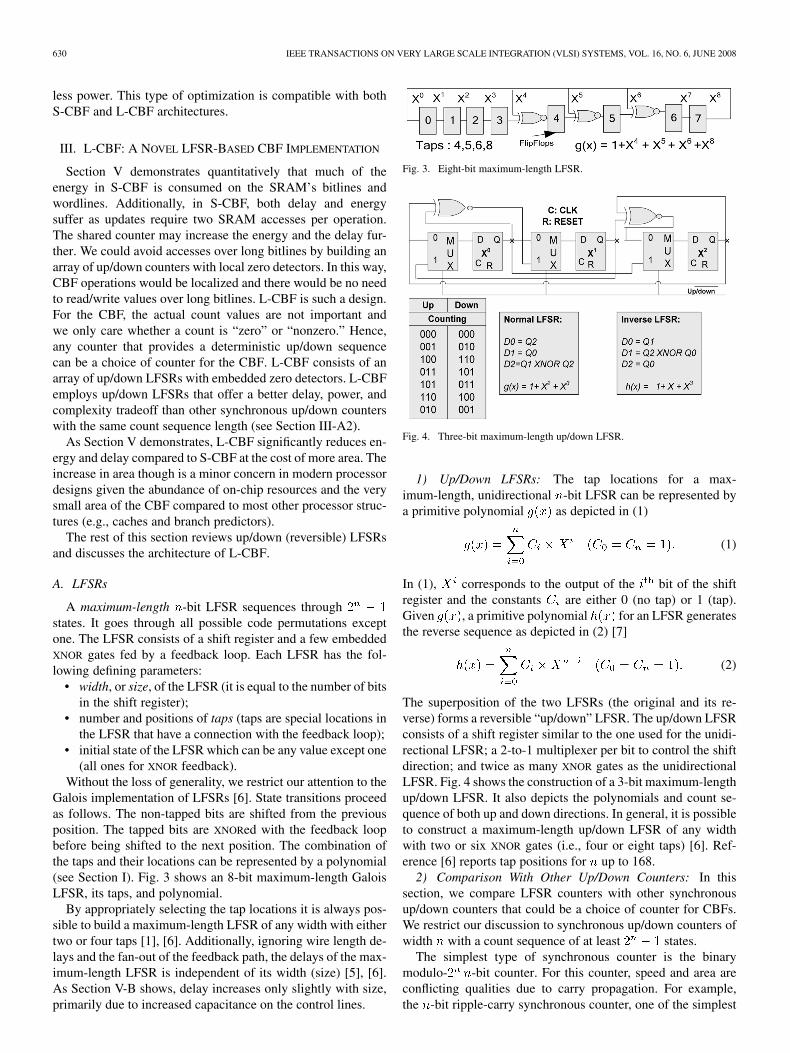
Without the loss of generality, we restrict our attention to theGalois implementation of LFSRs [6]. State transitions proceedas follows. The non-tapped bits are shifted from the previousposition. The tapped bits are XNORed with the feedback loopbefore being shifted to the next position. The combination ofthe taps and their locations can be represented by a polynomial(see Section I). Fig. 3 shows an 8-bit maximum-length GaloisLFSR, its taps, and polynomial.
By appropriately selecting the tap locations it is always pos-sible to build a maximum-length LFSR of any width with eithertwo or four taps [1], [6]. Additionally, ignoring wire length de-lays and the fan-out of the feedback path, the delays of the max-imum-length LFSR is independent of its width (size) [5], [6].As Section V-B shows, delay increases only slightly with size,primarily due to increased capacitance on the control lines.
Fig. 3. Eight-bit maximum-length LFSR.
Fig. 4. Three-bit maximum-length up/down LFSR.
1) Up/Down LFSRs: The tap locations for a max-imum-length, unidirectional -bit LFSR can be represented bya primitive polynomial as depicted in (1)
(1)
In (1), corresponds to the output of the bit of the shiftregister and the constants are either 0 (no tap) or 1 (tap).Given , a primitive polynomial for an LFSR generatesthe reverse sequence as depicted in (2) [7]
(2)
The superposition of the two LFSRs (the original and its re-verse) forms a reversible “up/down” LFSR. The up/down LFSRconsists of a shift register similar to the one used for the unidi-rectional LFSR; a 2-to-1 multiplexer per bit to control the shiftdirection; and twice as many XNOR gates as the unidirectionalLFSR. Fig. 4 shows the construction of a 3-bit maximum-lengthup/down LFSR. It also depicts the polynomials and count se-quence of both up and down directions. In general, it is possibleto construct a maximum-length up/down LFSR of any widthwith two or six XNOR gates (i.e., four or eight taps) [6]. Ref-erence [6] reports tap positions for up to 168.
2) Comparison With Other Up/Down Counters: In thissection, we compare LFSR counters with other synchronousup/down counters that could be a choice of counter for CBFs.We restrict our discussion to synchronous up/down counters ofwidth with a count sequence of at least states.
The simplest type of synchronous counter is the binarymodulo- -bit counter. For this counter, speed and area areconflicting qualities due to carry propagation. For example,the -bit ripple-carry synchronous counter, one of the simplest
SAFI et al.: L-CBF: A LOW-POWER, FAST COUNTING BLOOM FILTER ARCHITECTURE 631
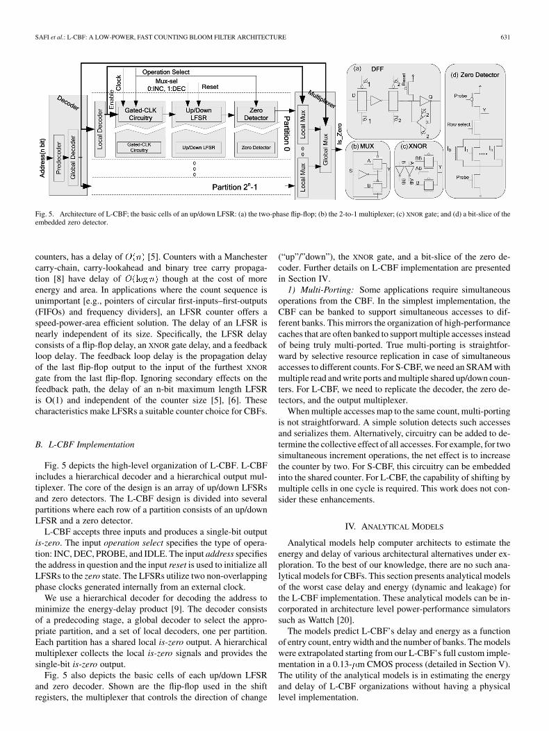
Fig. 5. Architecture of L-CBF; the basic cells of an up/down LFSR: (a) the two-phase flip-flop; (b) the 2-to-1 multiplexer; (c) XNOR gate; and (d) a bit-slice of theembedded zero detector.
counters, has a delay of [5]. Counters with a Manchestercarry-chain, carry-lookahead and binary tree carry propaga-tion [8] have delay of though at the cost of moreenergy and area. In applications where the count sequence isunimportant [e.g., pointers of circular first-inputs–first-outputs(FIFOs) and frequency dividers], an LFSR counter offers aspeed-power-area efficient solution. The delay of an LFSR isnearly independent of its size. Specifically, the LFSR delayconsists of a flip-flop delay, an XNOR gate delay, and a feedbackloop delay. The feedback loop delay is the propagation delayof the last flip-flop output to the input of the furthest XNOR
gate from the last flip-flop. Ignoring secondary effects on thefeedback path, the delay of an n-bit maximum length LFSRis O(1) and independent of the counter size [5], [6]. Thesecharacteristics make LFSRs a suitable counter choice for CBFs.
B. L-CBF Implementation
Fig. 5 depicts the high-level organization of L-CBF. L-CBFincludes a hierarchical decoder and a hierarchical output mul-tiplexer. The core of the design is an array of up/down LFSRsand zero detectors. The L-CBF design is divided into severalpartitions where each row of a partition consists of an up/downLFSR and a zero detector.
L-CBF accepts three inputs and produces a single-bit outputis-zero. The input operation select specifies the type of opera-tion: INC, DEC, PROBE, and IDLE. The input address specifiesthe address in question and the input reset is used to initialize allLFSRs to the zero state. The LFSRs utilize two non-overlappingphase clocks generated internally from an external clock.
We use a hierarchical decoder for decoding the address tominimize the energy-delay product [9]. The decoder consistsof a predecoding stage, a global decoder to select the appro-priate partition, and a set of local decoders, one per partition.Each partition has a shared local is-zero output. A hierarchicalmultiplexer collects the local is-zero signals and provides thesingle-bit is-zero output.
Fig. 5 also depicts the basic cells of each up/down LFSRand zero decoder. Shown are the flip-flop used in the shiftregisters, the multiplexer that controls the direction of change
(“up”/”down”), the XNOR gate, and a bit-slice of the zero de-coder. Further details on L-CBF implementation are presentedin Section IV.
1) Multi-Porting: Some applications require simultaneousoperations from the CBF. In the simplest implementation, theCBF can be banked to support simultaneous accesses to dif-ferent banks. This mirrors the organization of high-performancecaches that are often banked to support multiple accesses insteadof being truly multi-ported. True multi-porting is straightfor-ward by selective resource replication in case of simultaneousaccesses to different counts. For S-CBF, we need an SRAM withmultiple read and write ports and multiple shared up/down coun-ters. For L-CBF, we need to replicate the decoder, the zero de-tectors, and the output multiplexer.
When multiple accesses map to the same count, multi-portingis not straightforward. A simple solution detects such accessesand serializes them. Alternatively, circuitry can be added to de-termine the collective effect of all accesses. For example, for twosimultaneous increment operations, the net effect is to increasethe counter by two. For S-CBF, this circuitry can be embeddedinto the shared counter. For L-CBF, the capability of shifting bymultiple cells in one cycle is required. This work does not con-sider these enhancements.
IV. ANALYTICAL MODELS
Analytical models help computer architects to estimate theenergy and delay of various architectural alternatives under ex-ploration. To the best of our knowledge, there are no such ana-lytical models for CBFs. This section presents analytical modelsof the worst case delay and energy (dynamic and leakage) forthe L-CBF implementation. These analytical models can be in-corporated in architecture level power-performance simulatorssuch as Wattch [20].
The models predict L-CBF’s delay and energy as a functionof entry count, entry width and the number of banks. The modelswere extrapolated starting from our L-CBF’s full custom imple-mentation in a 0.13- m CMOS process (detailed in Section V).The utility of the analytical models is in estimating the energyand delay of L-CBF organizations without having a physicallevel implementation.
632 IEEE TRANSACTIONS ON VERY LARGE SCALE INTEGRATION (VLSI) SYSTEMS, VOL. 16, NO. 6, JUNE 2008
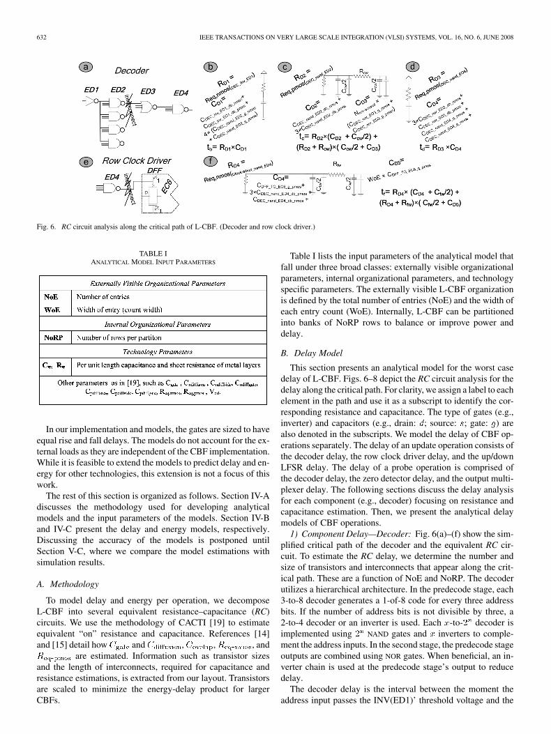
Fig. 6. RC circuit analysis along the critical path of L-CBF. (Decoder and row clock driver.)
TABLE IANALYTICAL MODEL INPUT PARAMETERS
In our implementation and models, the gates are sized to haveequal rise and fall delays. The models do not account for the ex-ternal loads as they are independent of the CBF implementation.While it is feasible to extend the models to predict delay and en-ergy for other technologies, this extension is not a focus of thiswork.
The rest of this section is organized as follows. Section IV-Adiscusses the methodology used for developing analyticalmodels and the input parameters of the models. Section IV-Band IV-C present the delay and energy models, respectively.Discussing the accuracy of the models is postponed untilSection V-C, where we compare the model estimations withsimulation results.
A. Methodology
To model delay and energy per operation, we decomposeL-CBF into several equivalent resistance–capacitance (RC)circuits. We use the methodology of CACTI [19] to estimateequivalent “on” resistance and capacitance. References [14]and [15] detail how and , , , and
are estimated. Information such as transistor sizesand the length of interconnects, required for capacitance andresistance estimations, is extracted from our layout. Transistorsare scaled to minimize the energy-delay product for largerCBFs.
Table I lists the input parameters of the analytical model thatfall under three broad classes: externally visible organizationalparameters, internal organizational parameters, and technologyspecific parameters. The externally visible L-CBF organizationis defined by the total number of entries (NoE) and the width ofeach entry count (WoE). Internally, L-CBF can be partitionedinto banks of NoRP rows to balance or improve power anddelay.
B. Delay Model
This section presents an analytical model for the worst casedelay of L-CBF. Figs. 6–8 depict the RC circuit analysis for thedelay along the critical path. For clarity, we assign a label to eachelement in the path and use it as a subscript to identify the cor-responding resistance and capacitance. The type of gates (e.g.,inverter) and capacitors (e.g., drain: ; source: ; gate: ) arealso denoted in the subscripts. We model the delay of CBF op-erations separately. The delay of an update operation consists ofthe decoder delay, the row clock driver delay, and the up/downLFSR delay. The delay of a probe operation is comprised ofthe decoder delay, the zero detector delay, and the output multi-plexer delay. The following sections discuss the delay analysisfor each component (e.g., decoder) focusing on resistance andcapacitance estimation. Then, we present the analytical delaymodels of CBF operations.
1) Component Delay—Decoder: Fig. 6(a)–(f) show the sim-plified critical path of the decoder and the equivalent RC cir-cuit. To estimate the RC delay, we determine the number andsize of transistors and interconnects that appear along the crit-ical path. These are a function of NoE and NoRP. The decoderutilizes a hierarchical architecture. In the predecode stage, each3-to-8 decoder generates a 1-of-8 code for every three addressbits. If the number of address bits is not divisible by three, a2-to-4 decoder or an inverter is used. Each -to- decoder isimplemented using NAND gates and inverters to comple-ment the address inputs. In the second stage, the predecode stageoutputs are combined using NOR gates. When beneficial, an in-verter chain is used at the predecode stage’s output to reducedelay.
The decoder delay is the interval between the moment theaddress input passes the INV(ED1)’ threshold voltage and the
SAFI et al.: L-CBF: A LOW-POWER, FAST COUNTING BLOOM FILTER ARCHITECTURE 633
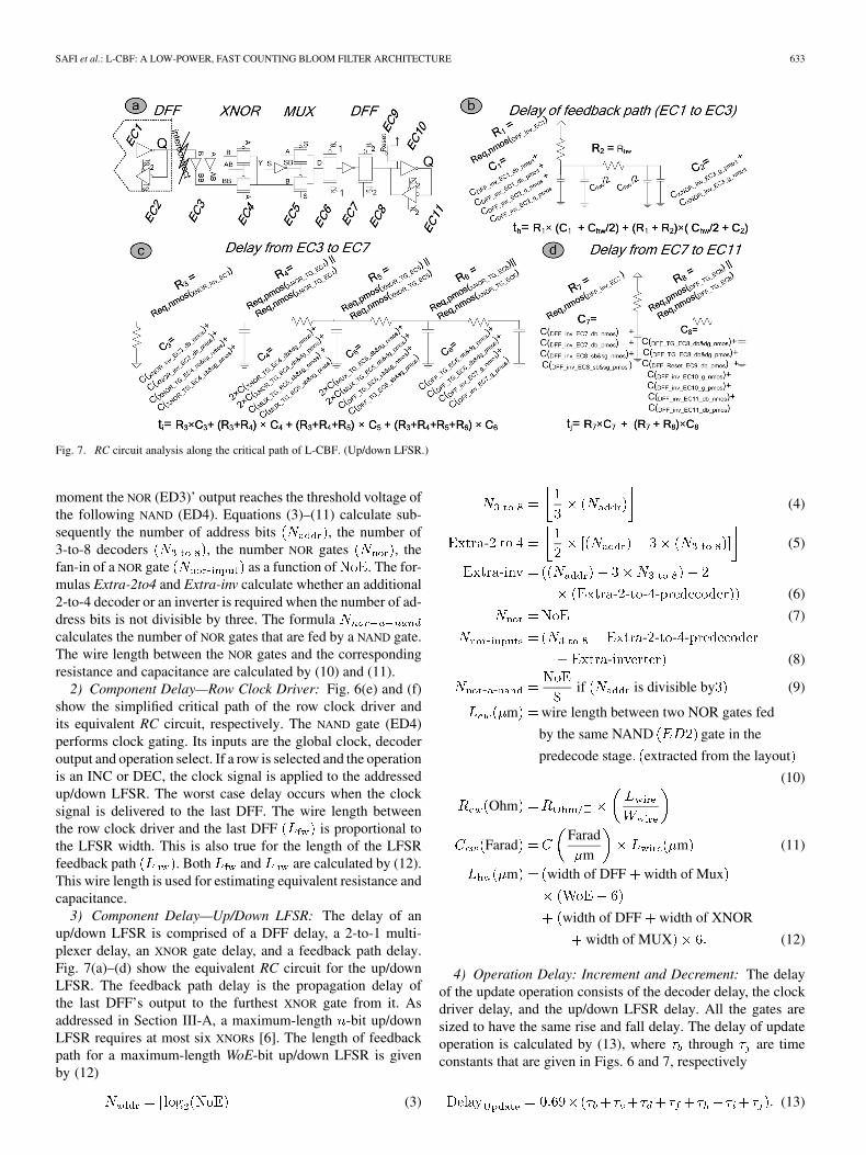
Fig. 7. RC circuit analysis along the critical path of L-CBF. (Up/down LFSR.)
moment the NOR (ED3)’ output reaches the threshold voltage ofthe following NAND (ED4). Equations (3)–(11) calculate sub-sequently the number of address bits , the number of3-to-8 decoders , the number NOR gates , thefan-in of a NOR gate as a function of . The for-mulas Extra-2to4 and Extra-inv calculate whether an additional2-to-4 decoder or an inverter is required when the number of ad-dress bits is not divisible by three. The formulacalculates the number of NOR gates that are fed by a NAND gate.The wire length between the NOR gates and the correspondingresistance and capacitance are calculated by (10) and (11).
2) Component Delay—Row Clock Driver: Fig. 6(e) and (f)show the simplified critical path of the row clock driver andits equivalent RC circuit, respectively. The NAND gate (ED4)performs clock gating. Its inputs are the global clock, decoderoutput and operation select. If a row is selected and the operationis an INC or DEC, the clock signal is applied to the addressedup/down LFSR. The worst case delay occurs when the clocksignal is delivered to the last DFF. The wire length betweenthe row clock driver and the last DFF is proportional tothe LFSR width. This is also true for the length of the LFSRfeedback path . Both and are calculated by (12).This wire length is used for estimating equivalent resistance andcapacitance.
3) Component Delay—Up/Down LFSR: The delay of anup/down LFSR is comprised of a DFF delay, a 2-to-1 multi-plexer delay, an XNOR gate delay, and a feedback path delay.Fig. 7(a)–(d) show the equivalent RC circuit for the up/downLFSR. The feedback path delay is the propagation delay ofthe last DFF’s output to the furthest XNOR gate from it. Asaddressed in Section III-A, a maximum-length -bit up/downLFSR requires at most six XNORs [6]. The length of feedbackpath for a maximum-length WoE-bit up/down LFSR is givenby (12)
(3)
(4)
- (5)
- - - - (6)
(7)
- - - -
- (8)
- - if is divisible by (9)
m wire length between two NOR gates fed
by the same NAND gate in the
predecode stage extracted from the layout
(10)
Ohm
FaradFarad
mm (11)
m width of DFF width of Mux
width of DFF width of XNOR
width of MUX (12)
4) Operation Delay: Increment and Decrement: The delayof the update operation consists of the decoder delay, the clockdriver delay, and the up/down LFSR delay. All the gates aresized to have the same rise and fall delay. The delay of updateoperation is calculated by (13), where through are timeconstants that are given in Figs. 6 and 7, respectively
(13)
634 IEEE TRANSACTIONS ON VERY LARGE SCALE INTEGRATION (VLSI) SYSTEMS, VOL. 16, NO. 6, JUNE 2008
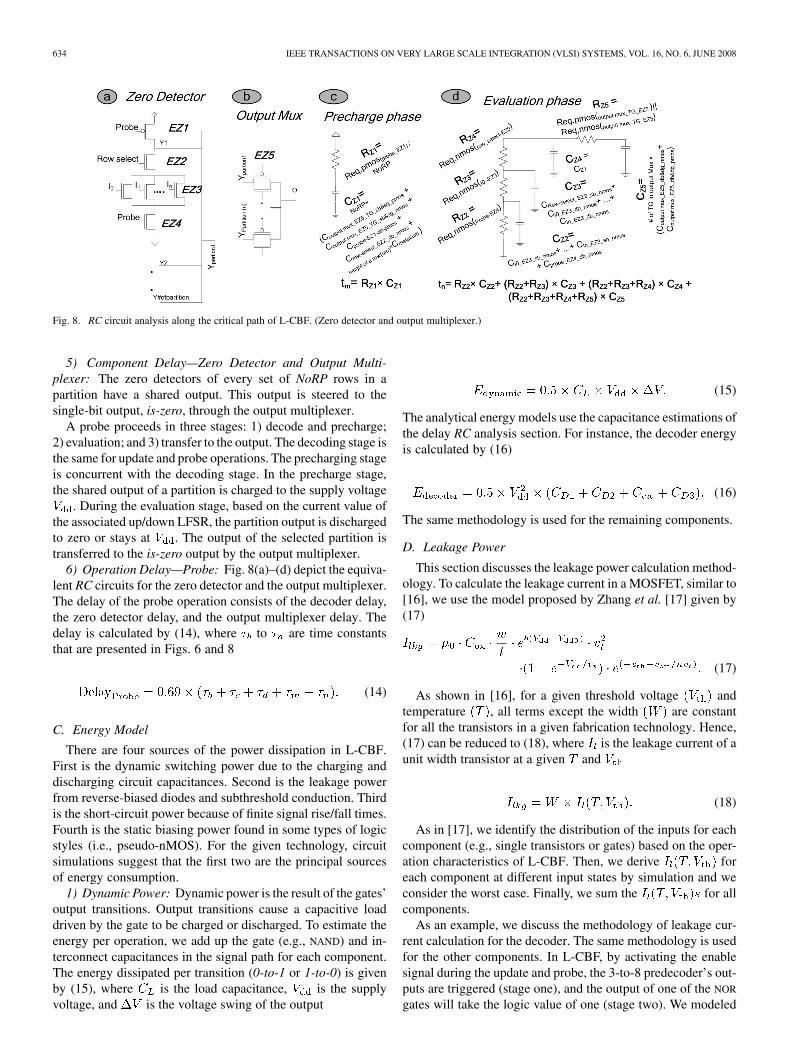
Fig. 8. RC circuit analysis along the critical path of L-CBF. (Zero detector and output multiplexer.)
5) Component Delay—Zero Detector and Output Multi-plexer: The zero detectors of every set of NoRP rows in apartition have a shared output. This output is steered to thesingle-bit output, is-zero, through the output multiplexer.
A probe proceeds in three stages: 1) decode and precharge;2) evaluation; and 3) transfer to the output. The decoding stage isthe same for update and probe operations. The precharging stageis concurrent with the decoding stage. In the precharge stage,the shared output of a partition is charged to the supply voltage
. During the evaluation stage, based on the current value ofthe associated up/down LFSR, the partition output is dischargedto zero or stays at . The output of the selected partition istransferred to the is-zero output by the output multiplexer.
6) Operation Delay—Probe: Fig. 8(a)–(d) depict the equiva-lent RC circuits for the zero detector and the output multiplexer.The delay of the probe operation consists of the decoder delay,the zero detector delay, and the output multiplexer delay. Thedelay is calculated by (14), where to are time constantsthat are presented in Figs. 6 and 8
(14)
C. Energy Model
There are four sources of the power dissipation in L-CBF.First is the dynamic switching power due to the charging anddischarging circuit capacitances. Second is the leakage powerfrom reverse-biased diodes and subthreshold conduction. Thirdis the short-circuit power because of finite signal rise/fall times.Fourth is the static biasing power found in some types of logicstyles (i.e., pseudo-nMOS). For the given technology, circuitsimulations suggest that the first two are the principal sourcesof energy consumption.
1) Dynamic Power: Dynamic power is the result of the gates’output transitions. Output transitions cause a capacitive loaddriven by the gate to be charged or discharged. To estimate theenergy per operation, we add up the gate (e.g., NAND) and in-terconnect capacitances in the signal path for each component.The energy dissipated per transition (0-to-1 or 1-to-0) is givenby (15), where is the load capacitance, is the supplyvoltage, and is the voltage swing of the output
(15)
The analytical energy models use the capacitance estimations ofthe delay RC analysis section. For instance, the decoder energyis calculated by (16)
(16)
The same methodology is used for the remaining components.
D. Leakage Power
This section discusses the leakage power calculation method-ology. To calculate the leakage current in a MOSFET, similar to[16], we use the model proposed by Zhang et al. [17] given by(17)
(17)
As shown in [16], for a given threshold voltage andtemperature , all terms except the width are constantfor all the transistors in a given fabrication technology. Hence,(17) can be reduced to (18), where is the leakage current of aunit width transistor at a given and
(18)
As in [17], we identify the distribution of the inputs for eachcomponent (e.g., single transistors or gates) based on the oper-ation characteristics of L-CBF. Then, we derive foreach component at different input states by simulation and weconsider the worst case. Finally, we sum the for allcomponents.
As an example, we discuss the methodology of leakage cur-rent calculation for the decoder. The same methodology is usedfor the other components. In L-CBF, by activating the enablesignal during the update and probe, the 3-to-8 predecoder’s out-puts are triggered (stage one), and the output of one of the NOR
gates will take the logic value of one (stage two). We modeled
SAFI et al.: L-CBF: A LOW-POWER, FAST COUNTING BLOOM FILTER ARCHITECTURE 635
the worst case leakage current in these two stages as given by(19) and (20), respectively. The leakage current for the decoderis given by (21). Multiplying the by gives the leakagepower estimation
(19)
(20)
(21)
V. EXPERIMENTAL RESULTS
This section compares the energy, delay, and area of S-CBFand L-CBF. Moreover, this section compares the analyticalmodel estimations against simulation results for L-CBF.
We compare S-CBF and L-CBF on a per operation basis.Both designs are implemented using the Cadence(R) tool set ina commercial 0.13- m fabrication technology. We developeda transistor-level implementation and a full-custom layout forboth designs that were optimized for the energy-delay product.We employed Spectre for circuit simulations. This is a vendorrecommended simulator for design validation prior to manufac-turing.
The rest of this section is organized as follows. We initiallyconsider a 1 K-entry CBF with 15-bit counts as this configura-tion is representative of the CBFs used in previous proposals[2], [4]. Then, we present results for other CBF configurations.In Section V-A, we compare the energy, delay and area ofthe two designs for all CBF operations (updates and probes).In Section V-B, we study how energy and delay change asthe number of entries and the width of the counters vary. InSection V-C, we discuss the accuracy of analytical models.
A. Delay and Energy Per Operation
We compare implementations of a 1 K-entry, 15-bit countper entry CBF. For S-CBF, an SRAM with a total capacity of15 Kbits is used. The SRAM is partitioned to minimize the en-ergy-delay product. For S-CBF, we do not consider the delayand energy overhead of the shared counter since our goal isto demonstrate that L-CBF consumes less energy and is alsofaster. To further reduce energy for probes in S-CBF, we in-troduce an extra bit per entry which is updated only when thecount changes from, or to, zero as described in Section II-B( -bits). On a probe, we only read this bit. Furthermore, weapply a number of delay and power optimizations on S-CBF[9]–[12]. In detail, we implement the divided word line (DWL)technique which adopts a two-stage hierarchical row decoderstructure. The DWL technique improves speed and power [10],[12]. Moreover, we reduce power further via pulse operationtechniques for the word-lines, the periphery circuits and thesense amplifiers [12]. We also use multistage static CMOS de-coding [9] and current-mode read and write operations to furtherreduce power [12]. For L-CBF, we utilize 16-bit LFSRs suchthat the LFSR can count at least values.
Table II shows the delay in picoseconds, the energy (static anddynamic) per operation in picojoules, and the area in square mil-limeters for both L-CBF and S-CBF. The last column reportsthe ratio of S-CBF over L-CBF per metric. The two rows percategory report, respectively, measurements for the update and
TABLE IIENERGY, DELAY, AND AREA OF S-CBF AND L-CBF IMPLEMENTATIONS FOR
A 1 K-ENTRY, 15-BIT CBF
probe operations. For delay and energy, we report the worst casewhich is measured by selecting appropriate inputs. The delayand energy of the shared counter of S-CBF is not included; oth-erwise, the actual delay and energy of S-CBF would be higher.
As observed from Table II, L-CBF is 3.7 and 1.6 faster thanS-CBF during update and probe operations, respectively. In ad-dition, L-CBF consumes 2.3 or 1.4 less energy than S-CBFfor update and probe operations, respectively. These significantgains in speed and energy consumption come at the expense ofmore area. L-CBF requires about 3.2 more area than S-CBF.However, as discussed in Section III, area is less of a concern inmodern microprocessor designs.
Disregarding the overhead (delay and energy) of the sharedcounter, the measurements for S-CBF are optimistic. Anup/down 15-bit LFSR counter has a delay of 240 ps and energyper update of 25 FJ. If this LFSR was used as the shared counterfor S-CBF, L-CBF would be 4.3 or 1.98 faster than S-CBFfor updates and probes, respectively (relative energy remainsvirtually the same).
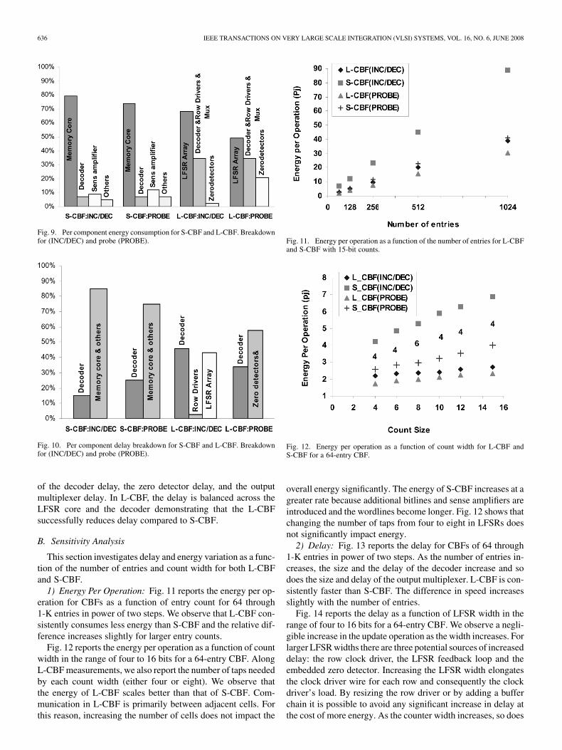
1) Per Component Energy Breakdown: Fig. 9 shows a percomponent breakdown of energy consumption for S-CBF andL-CBF. Most of the energy (79% and 74%, respectively, for up-dates and probes) in S-CBF is consumed by the memory core(worldlines, bitlines, and SRAM cells). The decoder and thesense-amplifiers consume considerably less energy. This is ex-pected as we applied aggressive energy and delay optimizationsto these components. For L-CBF, during probes, about 50% ofthe total energy is dissipated in inactive components, the LFSRarray and row drivers. For L-CBF, during updates, 50% of thetotal energy is dissipated in non-active LFSRs, row drivers, zerodetectors, and output multiplexer.
2) Per Component Delay Breakdown: Fig. 10 shows a percomponent breakdown of delay for both S-CBF and L-CBF forupdates and probes. In S-CBF, the update operation delay con-sists of the decoder delay, the SRAM read access delay (ex-cluding the decoder delay) and the SRAM write access delay(excluding the decoder delay). In detail, the update operationdelay consists of the decoder delay, the read-wordline delay,the read-bitline delay, the read-sense amplifier delay, the read-output multiplexer delay, the write-write driver delay, the write-wordline delay, the write-bitline delay, and the precharge delay.The precharge delay is included as the update operation involvesa read-modify-write sequence. In S-CBF, significant part of thedelay belongs to the memory core, demonstrating that signifi-cant potential exists for improvements with L-CBF.
For L-CBF, the delay of the update operation consists of thedecoder delay, the row clock driver delay, and the up/downLFSR delay. For L-CBF, the probe operation delay is comprised
636 IEEE TRANSACTIONS ON VERY LARGE SCALE INTEGRATION (VLSI) SYSTEMS, VOL. 16, NO. 6, JUNE 2008
Fig. 9. Per component energy consumption for S-CBF and L-CBF. Breakdownfor (INC/DEC) and probe (PROBE).
Fig. 10. Per component delay breakdown for S-CBF and L-CBF. Breakdownfor (INC/DEC) and probe (PROBE).
of the decoder delay, the zero detector delay, and the outputmultiplexer delay. In L-CBF, the delay is balanced across theLFSR core and the decoder demonstrating that the L-CBFsuccessfully reduces delay compared to S-CBF.
B. Sensitivity Analysis
This section investigates delay and energy variation as a func-tion of the number of entries and count width for both L-CBFand S-CBF.
1) Energy Per Operation: Fig. 11 reports the energy per op-eration for CBFs as a function of entry count for 64 through1-K entries in power of two steps. We observe that L-CBF con-sistently consumes less energy than S-CBF and the relative dif-ference increases slightly for larger entry counts.
Fig. 12 reports the energy per operation as a function of countwidth in the range of four to 16 bits for a 64-entry CBF. AlongL-CBF measurements, we also report the number of taps neededby each count width (either four or eight). We observe thatthe energy of L-CBF scales better than that of S-CBF. Com-munication in L-CBF is primarily between adjacent cells. Forthis reason, increasing the number of cells does not impact the
Fig. 11. Energy per operation as a function of the number of entries for L-CBFand S-CBF with 15-bit counts.
Fig. 12. Energy per operation as a function of count width for L-CBF andS-CBF for a 64-entry CBF.
overall energy significantly. The energy of S-CBF increases at agreater rate because additional bitlines and sense amplifiers areintroduced and the wordlines become longer. Fig. 12 shows thatchanging the number of taps from four to eight in LFSRs doesnot significantly impact energy.
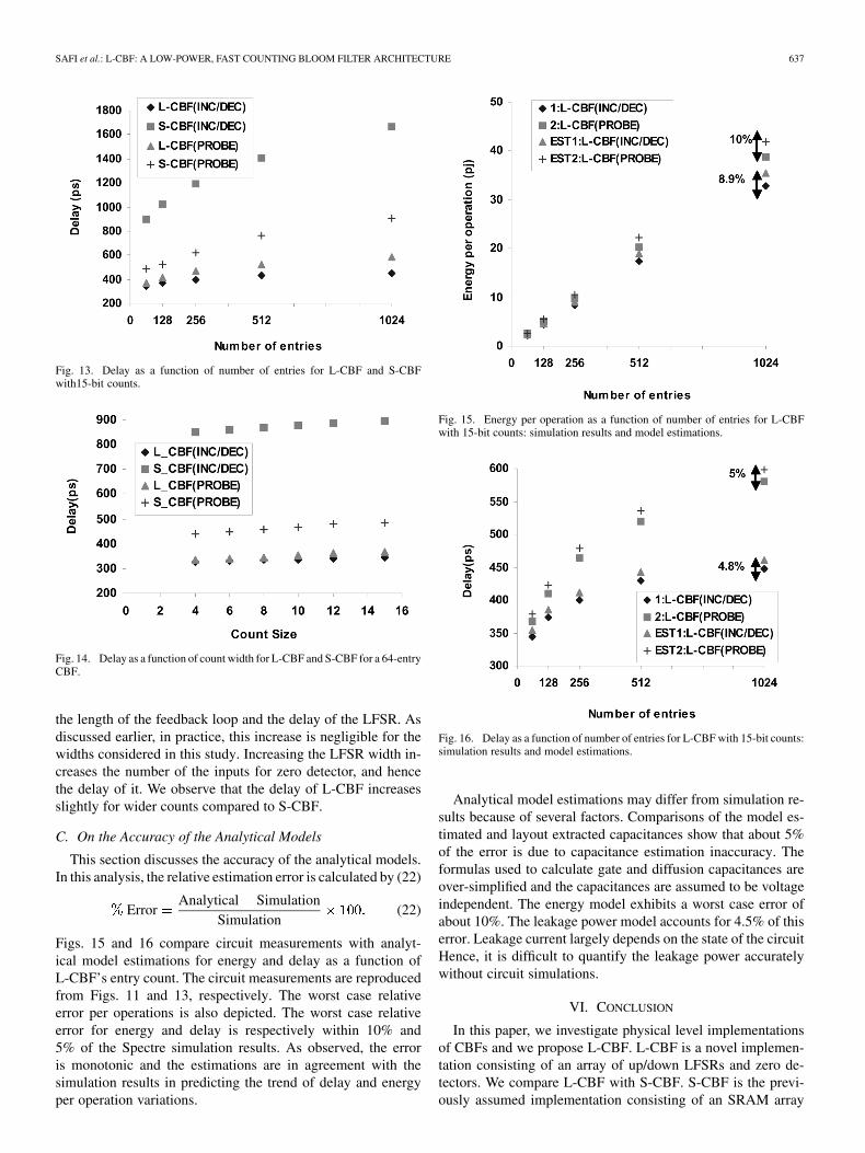
2) Delay: Fig. 13 reports the delay for CBFs of 64 through1-K entries in power of two steps. As the number of entries in-creases, the size and the delay of the decoder increase and sodoes the size and delay of the output multiplexer. L-CBF is con-sistently faster than S-CBF. The difference in speed increasesslightly with the number of entries.
Fig. 14 reports the delay as a function of LFSR width in therange of four to 16 bits for a 64-entry CBF. We observe a negli-gible increase in the update operation as the width increases. Forlarger LFSR widths there are three potential sources of increaseddelay: the row clock driver, the LFSR feedback loop and theembedded zero detector. Increasing the LFSR width elongatesthe clock driver wire for each row and consequently the clockdriver’s load. By resizing the row driver or by adding a bufferchain it is possible to avoid any significant increase in delay atthe cost of more energy. As the counter width increases, so does
SAFI et al.: L-CBF: A LOW-POWER, FAST COUNTING BLOOM FILTER ARCHITECTURE 637
Fig. 13. Delay as a function of number of entries for L-CBF and S-CBFwith15-bit counts.
Fig. 14. Delay as a function of count width for L-CBF and S-CBF for a 64-entryCBF.
the length of the feedback loop and the delay of the LFSR. Asdiscussed earlier, in practice, this increase is negligible for thewidths considered in this study. Increasing the LFSR width in-creases the number of the inputs for zero detector, and hencethe delay of it. We observe that the delay of L-CBF increasesslightly for wider counts compared to S-CBF.
C. On the Accuracy of the Analytical Models
This section discusses the accuracy of the analytical models.In this analysis, the relative estimation error is calculated by (22)
ErrorAnalytical Simulation
Simulation(22)
Figs. 15 and 16 compare circuit measurements with analyt-ical model estimations for energy and delay as a function ofL-CBF’s entry count. The circuit measurements are reproducedfrom Figs. 11 and 13, respectively. The worst case relativeerror per operations is also depicted. The worst case relativeerror for energy and delay is respectively within 10% and5% of the Spectre simulation results. As observed, the erroris monotonic and the estimations are in agreement with thesimulation results in predicting the trend of delay and energyper operation variations.
Fig. 15. Energy per operation as a function of number of entries for L-CBFwith 15-bit counts: simulation results and model estimations.
Fig. 16. Delay as a function of number of entries for L-CBF with 15-bit counts:simulation results and model estimations.
Analytical model estimations may differ from simulation re-sults because of several factors. Comparisons of the model es-timated and layout extracted capacitances show that about 5%of the error is due to capacitance estimation inaccuracy. Theformulas used to calculate gate and diffusion capacitances areover-simplified and the capacitances are assumed to be voltageindependent. The energy model exhibits a worst case error ofabout 10%. The leakage power model accounts for 4.5% of thiserror. Leakage current largely depends on the state of the circuitHence, it is difficult to quantify the leakage power accuratelywithout circuit simulations.
VI. CONCLUSION
In this paper, we investigate physical level implementationsof CBFs and we propose L-CBF. L-CBF is a novel implemen-tation consisting of an array of up/down LFSRs and zero de-tectors. We compare L-CBF with S-CBF. S-CBF is the previ-ously assumed implementation consisting of an SRAM array
638 IEEE TRANSACTIONS ON VERY LARGE SCALE INTEGRATION (VLSI) SYSTEMS, VOL. 16, NO. 6, JUNE 2008
of counts and a shared counter. We evaluate the energy, delay,and area of L-CBF and S-CBF in a commercial fabrication tech-nology. L-CBF is superior to S-CBF in both delay and speed atthe expense of more area. Additionally, we present analyticaldelay and energy models for L-CBF. These models facilitateestimation of the delay and energy variation for CBFs duringarchitectural level investigations when physical level implemen-tation is not yet available. Comparisons demonstrate that the es-timations provided by the models are in satisfying agreementwith the simulation results.
ACKNOWLEDGMENT
The authors would like to thank the anonymous reviewers ofthis paper and the reviewers of its earlier conference version fortheir helpful comments. The authors would also like to thank M.Haji Rostam and N. Azizi for their help in physical-level designand simulation.
REFERENCES
[1] A. Moshovos, “RegionScout: Exploiting coarse-grain sharing insnoop-coherence,” in Proc. Ann. Int. Symp. Comput. Arch., Jun. 2005,pp. 234–245.
[2] A. Moshovos, G. Memik, B. Falsafi, and A. Choudhary, “Jetty:Filtering snoops for reduced energy consumption in smp servers,” inProc. Ann. Int. Conf. High-Performance Comput. Arch., Feb. 2001,pp. 85–96.
[3] S. Sethumadhavan, R. Desikan, D. Burger, C. R. Moore, and S. W.Keckler, “Scalable hardware memory disambiguation for high-ILPprocessors,” IEEE Micro, vol. 24, no. 6, pp. 118–127, Nov. 2004.
[4] J. K. Peir, S. C. Lai, S. L. Lu, J. Stark, and K. Lai, “Bloom filteringcache misses for accurate data speculation and prefetching,” in Proc.Ann. Int. Conf. Supercomput., Jun. 2002, pp. 189–198.
[5] M. R. Stan, “Synchronous up/down counter with clock period inde-pendent of counter size,” in Proc. Ann. Symp. Comput. Arithmetic, Jul.1997, pp. 274–281.
[6] P. Alfke, “Efficient shift registers, LFSR counters, and long pseudo-random sequence generators,” Xilinx, San Jose, CA, Appl. Note 052,Jul. 1996.
[7] P. H. Bardell, W. H. McAnney, and J. Savir, Built-in test for VLSI:Pseudorandom techniques. New York: Wiley, 1987.
[8] M. R. Stan, A. F. Tenca, and M. D. Ercegovac, “Long and fast up/downcounters,” IEEE Trans. Comput., vol. 47, no. 7, pp. 722–735, Jul. 1998.
[9] B. S. Amrutur and M. A. Horowitz, “Fast low-power decoders forRAMs,” IEEE J. Solid-State Circuits, vol. 36, no. 10, pp. 1506–1515,Oct. 2001.
[10] B. S. Amrutur, “Design and analysis of fast low power SRAMs,” Ph.D.dissertation, Elect. Eng. Dept., Stanford Univ., Stanford, CA, 1999.
[11] B. S. Amrutur and M. A. Horowitz, “Speed and power scaling ofSRAM’s,” IEEE J. Solid-State Circuits, vol. 35, no. 2, pp. 175–185,Feb. 2000.
[12] M. Margala, “Low-power SRAM circuit design,” in Proc. IEEE Work-shop Memory Technol., Design Test., Aug. 1999, pp. 115–122.
[13] D. Burger and T. Austin, The Simplescalar Tool Set v2.0 Comput. Sci.Dept., Univ. Wisconsin-Madison, Madison, Tech. Rep. UW-CS-97-1342, 1997.
[14] H. E. W. Neil and D. Harris, Principles of CMOS VLSI Design, 3rded. Reading, MA: Addison Wesley, 2004.
[15] D. A. Hodges, H. G. Jackson, and R. A. Saleh, Analysis and Design ofDigital Integrated Circuits, 3rd ed. New York: McGraw-Hill, 2004.
[16] M. Mamidipaka, K. Khouri, N. Dutt, and M. Abadir, “Analyticalmodels for leakage power estimation of memory array structures,” inProc. Int. Conf. Hardw./Softw. Co-Design Syst. Synth., Sep. 2004, pp.146–151.
[17] Y. Zhang, D. Parikh, K. Sankaranarayanan, K. Skadron, and M. Stan,“Hotleakage: A temperature-aware model of subthreshold and gateleakage for architects,” Univ. Virginia, Charlottesville, Tech. Rep.CS-2003-05, 2003.
[18] X. N. Chen and L. S. Peh, “Leakage power modeling and optimizationof interconnection network,” in Proc. Int. Symp. Low Power Electron.Des., Aug. 2003, pp. 90–95.
[19] S. Wilton and N. Jouppi, “An enhanced access and cycle time modelfor on-chip caches,” 1994.
[20] D. Brooks, V. Tiwari, and M. Martonosi, “Wattch: A framework forarchitectural level power analysis and optimizations,” in Proc. Ann. Int.Symp. Comput. Arch., Jun. 2000, pp. 83–94.
[21] E. Safi, A. Moshovos, and A. Veneris, “L-CBF: A fast, low-powercounting bloom filter architecture,” in Proc. Ann. Int. Symp. Low PowerElectron. Des., Oct. 2006, pp. 250–255.
Elham Safi (S’05) received the B.Sc. and M.Sc. de-grees in computer hardware engineering and com-puter architecture from the University of Tehran, Iran.She is currently pursuing the Ph.D. degree in elec-trical and computer engineering from the Universityof Toronto, Toronto, ON, Canada.
Her research interests include computer architec-ture with emphasis on hardware design and imple-mentation.
Andreas Moshovos (S’96–M’99–SM’05) receivedthe Ptyhion degree and the M.Sc. degree in computerscience from the University of Crete, Hellas, Greece,and the Ph.D. degree in computer science from theUniversity of Wisconsin-Madison, Madison.
He is an Associate Professor with the Departmentof Electrical and Computer Engineering, Universityof Toronto. His research interests include microarchi-tectural optimizations for high-performance proces-sors and systems.
He is a member of the Association for ComputingMachinery (ACM).
Andreas Veneris (S’96–M’99–SM’05) received theDiploma in computer engineering and informaticsfrom the University of Patras, Patras, Greece, theM.S. degree in computer science from the Universityof Southern California, Los Angeles, and the Ph.D.degree in computer science from the University ofIllinois at Urbana-Champaign (UIUC), Urbana.
He is currently an Associate Professor, cross-ap-pointed with the Department of Electrical and Com-puter Engineering and Department of Computer Sci-ence, University of Toronto, Toronto, ON, Canada.
His research interests include computer-aided design for the debugging, verifi-cation, synthesis and test of digital circuits and systems as well as data structuresand combinatorics.
He is a member of the Association for Computing Machinery (ACM), theAmerican Association for the Advancement of Science (AAAS), the TechnicalChamber of Greece, and the Planetary Society.