Embed Size (px)
Citation preview
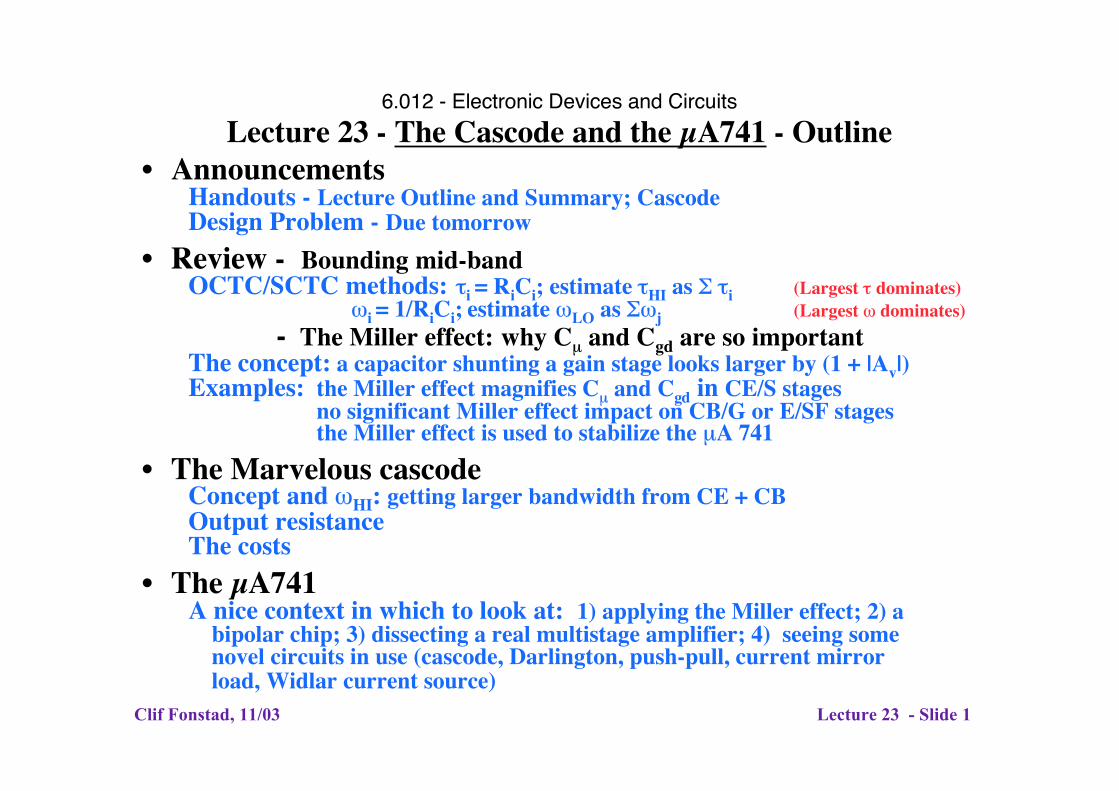
6.012 - Electronic Devices and Circuits
Lecture 23 - The Cascode and the µA741 - Outline • Announcements
Handouts - Lecture Outline and Summary; CascodeDesign Problem - Due tomorrow
• Review - Bounding mid-bandOCTC/SCTC methods: ti = RiCi; estimate tHI as S ti (Largest t dominates)
wi = 1/RiCi; estimate wLO as Swj (Largest w dominates)
- The Miller effect: why C m and Cgd are so important The concept: a capacitor shunting a gain stage looks larger by (1 + |Av|) Examples: the Miller effect magnifies Cm and Cgd in CE/S stages
no significant Miller effect impact on CB/G or E/SF stages the Miller effect is used to stabilize the mA 741
• The Marvelous cascodeConcept and wHI: getting larger bandwidth from CE + CBOutput resistanceThe costs
• The µA741A nice context in which to look at: 1) applying the Miller effect; 2) a
bipolar chip; 3) dissecting a real multistage amplifier; 4) seeing some novel circuits in use (cascode, Darlington, push-pull, current mirror load, Widlar current source)
Clif Fonstad, 11/03 Lecture 23 - Slide 1
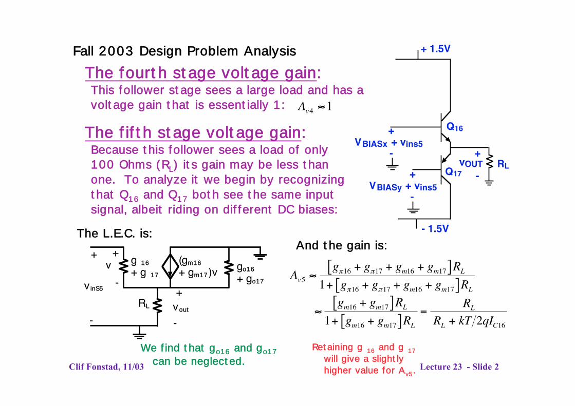
Q16
Q17
- 1.5V
+
-VBIASx + vins5
vOUT+
-+
-VBIASy + vins5
+ 1.5VFall 2003 Design Problem Analysis The fourth stage voltage gain: This follower stage sees a large load and has avoltage gain that is essentially 1: ª 1Av 4
The fifth stage voltage gain: Because this follower sees a load of only100 Ohms (RL) its gain may be less than RL
one. To analyze it we begin by recognizingthat Q16 and Q17 both see the same inputsignal, albeit riding on different DC biases:
The L.E.C. is: And the gain is:
(g+ g )v
m16
m17
+ + g 16 v go16 [gp16 + gp17 + gm16 + gm17 ] RL+ g 17 ª+ go17
Av 5-v inS5 1 + [gp16 + gp17 + gm16 + gm17 ] RL+ RL vout [gm16 + gm17 ] RL RLª =
- - 1 + [gm16 + gm17 ] RL RL + kT 2qIC16
We find that go16 and go17 Retaining g 16 and g 17
can be neglected. will give a slightly Lecture 23 - Slide 2 Clif Fonstad, 11/03 higher value for Av5.
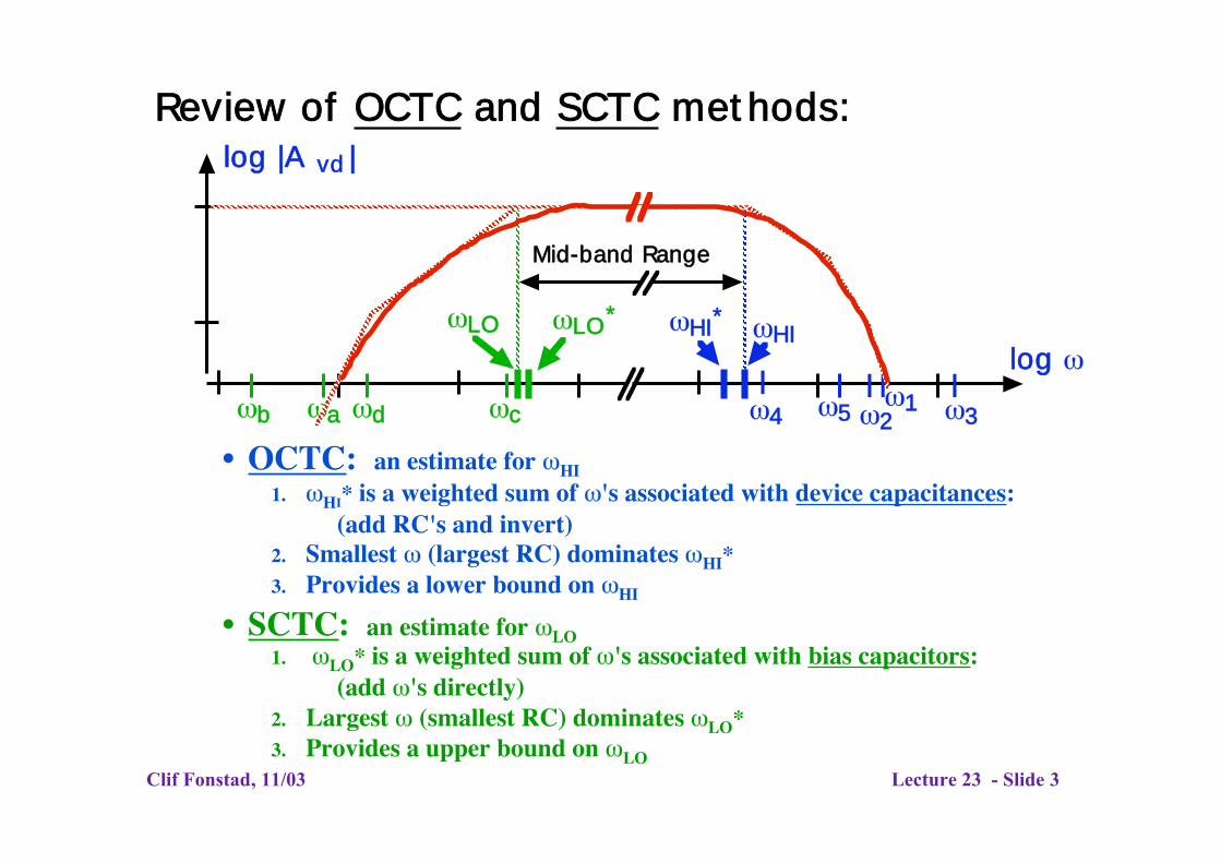
Review of OCTC and SCTC methods:
l w
l |A |
wb wcwdwa
w w *
w4 w5 w2 w1 w3
wHI * wHI
Mi
og
og vd
LO LO
d-band Range
• OCTC: an estimate for wHI
1. wHI* is a weighted sum of w's associated with device capacitances: (add RC's and invert)
2. Smallest w (largest RC) dominates wHI* 3. Provides a lower bound on wHI
• SCTC: an estimate for wLO 1. wLO* is a weighted sum of w's associated with bias capacitors:
(add w's directly) 2. Largest w (smallest RC) dominates wLO* 3. Provides a upper bound on wLO
Clif Fonstad, 11/03 Lecture 23 - Slide 3
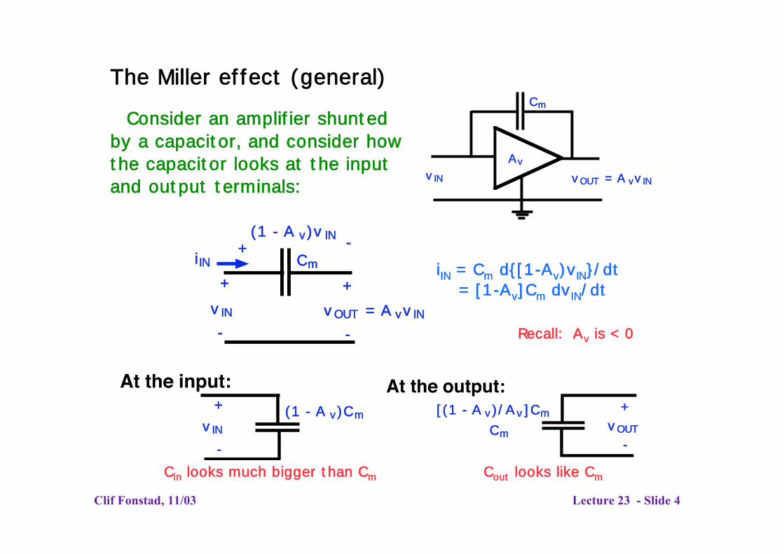
The Miller effect (general) Cm
Consider an amplifier shunted by a capacitor, and consider how
Avthe capacitor looks at the input vOUT = A vvINand output terminals:
vIN
(1 - A v)v IN -+iIN Cm i N = Cm d{[1-Av)v N}/dt I I+ + = [1-Av]Cm dv N/dt Iv IN vOUT = A vvIN - - Recall: Av is < 0
At the input: At the output: + +(1 - A v)Cm [(1 - A v)/Av]Cm
vOUT v IN Cm --
Cin looks much bigger than Cm Cout looks like Cm
Clif Fonstad, 11/03 Lecture 23 - Slide 4
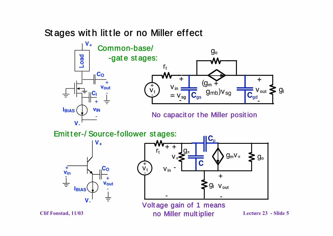
Stages with little or no Miller effect V+ Common-base/ go
-gate stages:
CO
+ vout
(gm + gmb)vsg
+
-
v in = v
+
-
vv t +
-
rt
C Csg out
gs gd glCI -
+ vINIBIAS - No capacitor the Miller position
V-
Emitter-/Source-follower stages: V+
+ COvin- +
voutIBIAS -
V
C
Cµ
gp +
-
vp gmvp go
gl
+
-
v in +
-
v
v t +
-
rt
out
- Voltage gain of 1 means Clif Fonstad, 11/03 no Miller multiplier Lecture 23 - Slide 5
--
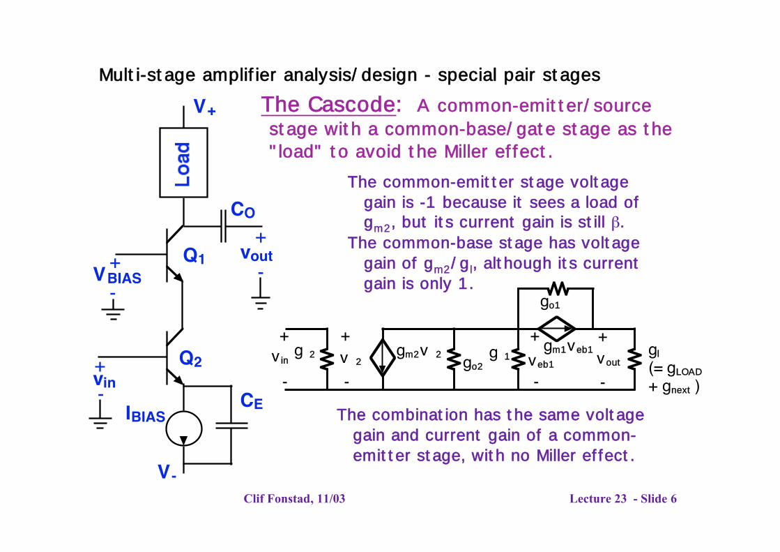
Multi-stage amplifier analysis/design - special pair stages
gl (= gLOAD + gnext )
: ii
"l i illi l
in i i lg i in i ill b.
li l l iin i l
V+
VBIAS
vout +
-
CO
+
-
vin + Q2
Q1
g 2
+
-
v 2 g v 2
g
+
-
v in
+ vg 1
+
vg v
g
The Cascode A common-em tter/source stage w th a common-base/gate stage as the
oad" to avo d the M er effect. The common-em tter stage vo tage
ga s -1 because t sees a oad of m2, but ts current ga s st
The common-base stage has vo tage ga n of gm2/g , a though ts current ga s on y 1.
m2o2 out eb1
m1 eb1
o1
The combination has the same voltage gain and current gain of a common-emitter stage, with no Miller effect.
-IBIAS
V-
CE
Clif Fonstad, 11/03 Lecture 23 - Slide 6
- - - - - - - - - - - -
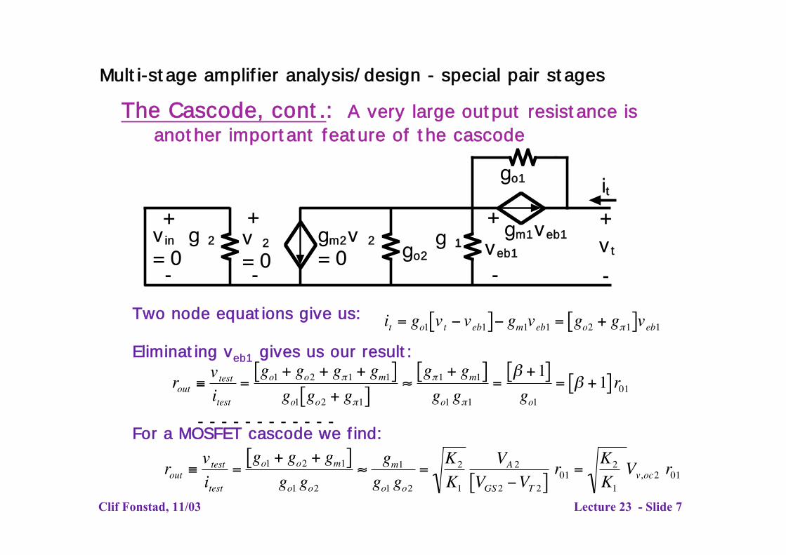
Multi-stage amplifier analysis/design - special pair stages
The Cascode, cont.: A very large output resistance is another i
g 2
+
-
v 2 = 0
g v 2 = 0 g
+
-
v in = 0
+
-
v tg 1
+
-v
g v
git
mportant feature of the cascode
m2o2 eb1
m1 eb1
o1
Two node equations give us: it = go1[vt - veb1]- gm1veb1 = [go2 + gp1]veb1
Eliminating veb1 gives us our result:
rout ≡ vtest [go1 + go2 + gp1 + gm1] [gp1 + gm1] =
[b +1] i
= ª = [b +1] r01 test go1[go2 + gp1] go1 gp1 go1
For a MOSFET cascode we find: v K2 VA 2 K2rout ≡ test [go1 + go2 + gm1] ª
gm1= = =r01 Vv,oc 2 r01K1itest go1 go2 go1 go2 K1 [VGS 2 -VT 2 ] Clif Fonstad, 11/03 Lecture 23 - Slide 7
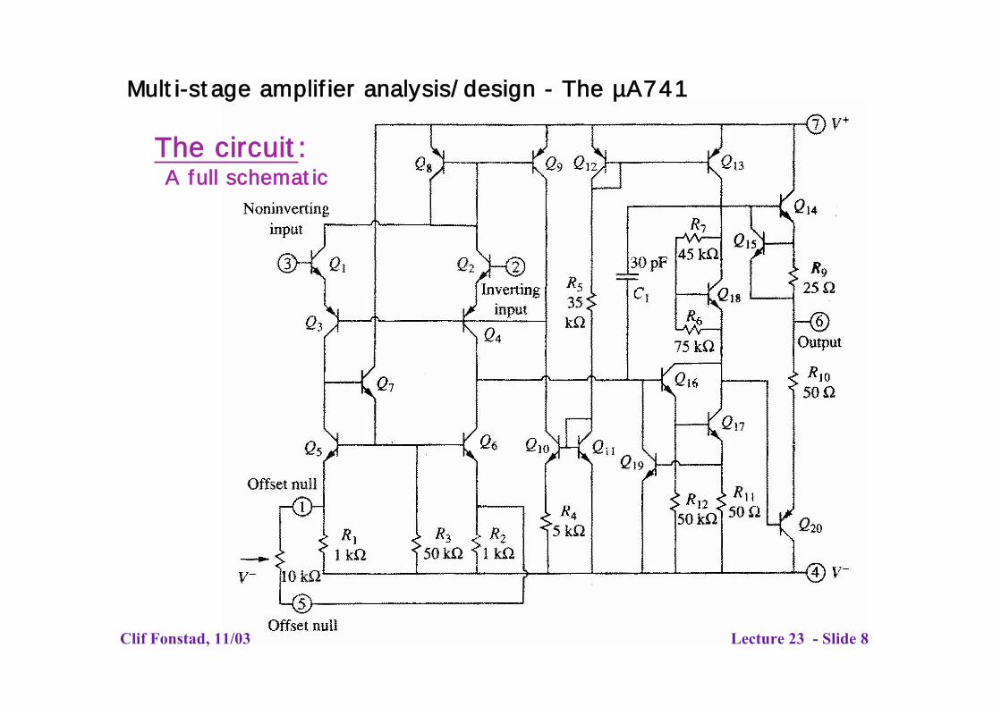
lti lifi l i i
i it: ll ic
Mu -stage amp er ana ys s/des gn - The µA741
Clif Fonstad, 11/03 Lecture 23 - Slide 8
The c rcuA fu schemat
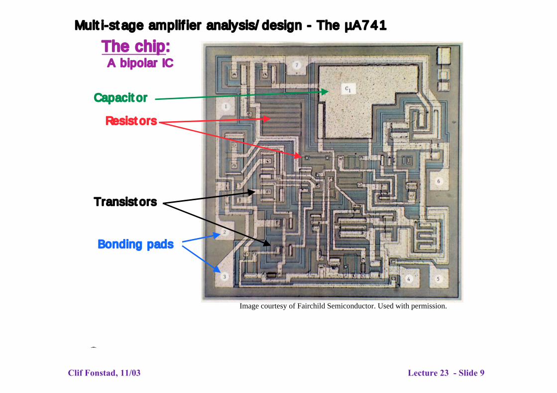
Multi-stage amplifier analysis/design - The µA741
ip: i l IC
i
i
i
i
Image courtesy of Fairchild Semiconductor. Used with permission.
The chA b po ar
Trans stors
Capac tor
Res stors
Bond ng pads
Clif Fonstad, 11/03 Lecture 23 - Slide 9
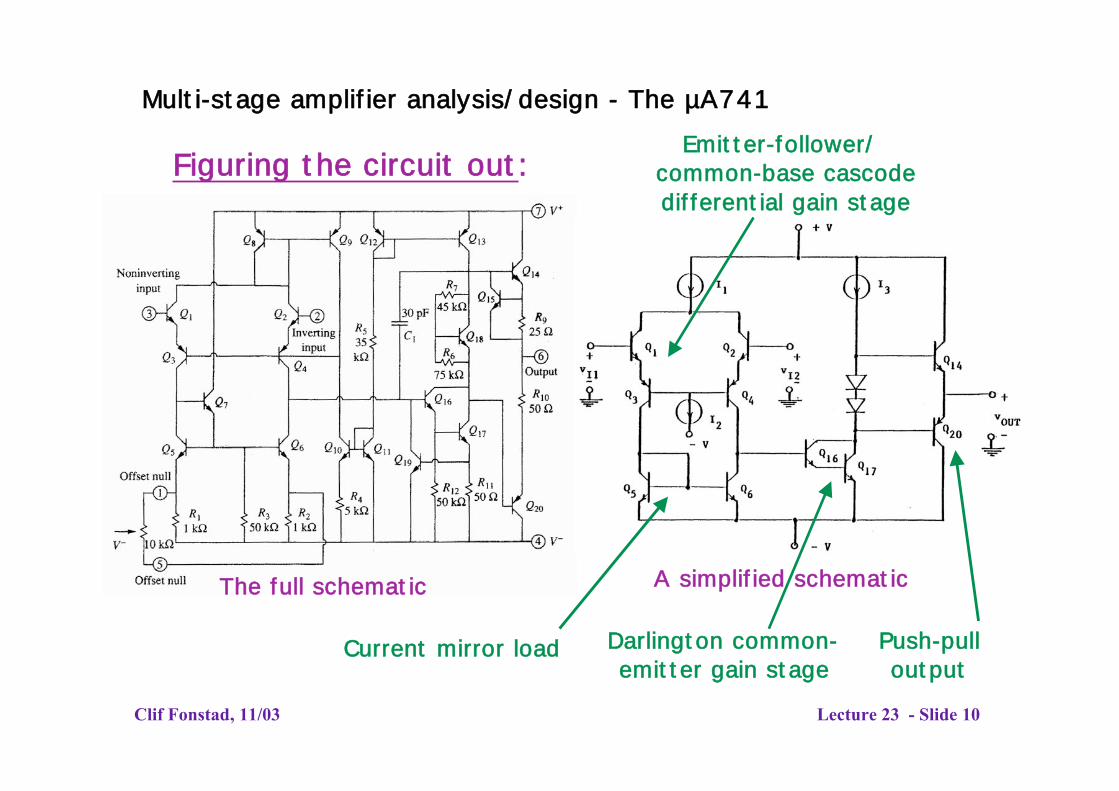
Multi-stage amplifier analysis/design - The µA741 Emitter-follower/
Figuring the circuit out: common-base cascode
ll ic i lifi ic
li
di ial i
ll
The fu schemat A s mp ed schemat
Dar
fferent ga n stage
Push-pungton common-Current mirror load emitter gain stage output
Clif Fonstad, 11/03 Lecture 23 - Slide 10
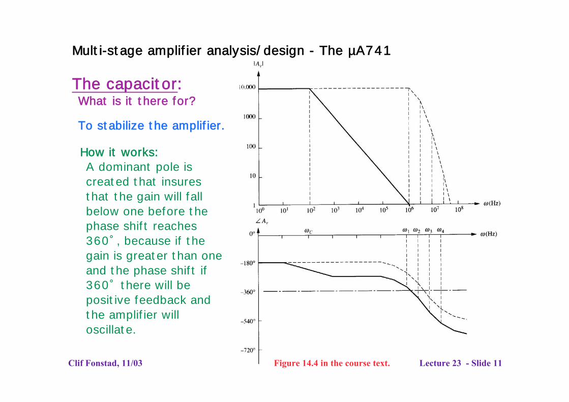
Multi-stage amplifier analysis/design - The µA741
The capacitor: What is it there for?
To stabilize the amplifier.
How it works:A dominant pole iscreated that insuresthat the gain will fallbelow one before thephase shift reaches360˚, because if thegain is greater than oneand the phase shift if360˚ there will bepositive feedback andthe amplifier willoscillate.
Clif Fonstad, 11/03 Lecture 23 - Slide 11 Figure 14.4 in the course text.
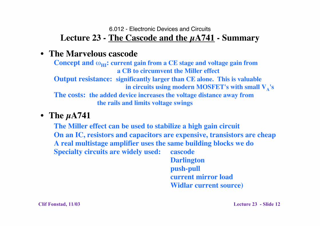
6.012 - Electronic Devices and Circuits
Lecture 23 - The Cascode and the µA741 - Summary
• The Marvelous cascode Concept and wHI: current gain from a CE stage and voltage gain from
a CB to circumvent the Miller effect Output resistance: significantly larger than CE alone. This is valuable
in circuits using modern MOSFET's with small VA's The costs: the added device increases the voltage distance away from
the rails and limits voltage swings
• The µA741The Miller effect can be used to stabilize a high gain circuit On an IC, resistors and capacitors are expensive, transistors are cheap A real multistage amplifier uses the same building blocks we do Specialty circuits are widely used: cascode
Darlington push-pull current mirror load Widlar current source)
Clif Fonstad, 11/03 Lecture 23 - Slide 12