Embed Size (px)
Citation preview
All Digital Polar Transmitter Design for Software Defined Radio
-- Architecture and Low Power Circuit Implementations
Liang Rong
Doctoral Thesis in Electronic and Computer Systems
Stockholm, Sweden, 2012
Liang Rong
All Digital Polar Transmitter Design for Software Defined Radio
-- Architecture and Low Power Circuit Implementations
Doctoral dissertation submitted to Royal Institute of Technology (KTH) in
partial fulfillment of the requirements for the degree of Doctor of
Technology (Dr. Tech).
ISBN 978-91-7501-614-6
TRITA-ICT/ES AVH 12:10
ISSN 1653-6363
ISRN KTH/ICT/ECS/AVH-12/10-SE
Copyright © Liang Rong, December 2012
Contact: [email protected]
Royal Institute of Technology (KTH), Sweden
School of Information and Communication Technology
Department of Electronic Systems
Forum 120, Isafjordsgatan 39
SE-164 40 Kista, Stockholm
Sweden
Royal Institute of Technology (KTH) Sweden, Ph.D. Thesis
Abstract
The evolving wireless communication technology is aiming high
data rate, high mobility, long distance and at the meantime, co-exist
with various different standards. This developing trend requires a
highly linear transceiver system and it causes the problem of low
efficiency due to the large crest factor of signals. On the other hand,
with process scaling, digital blocks are occupying more functions and
chip area than before, to fully utilize the digital process low power
advantage and save design cost, hardware reuse is preferable. The
concept of Software Defined Radio (SDR) is raised to make the
system more adaptable to multiple communication standards with
minimal hardware resources.
In this doctoral dissertation work, the software defined radio
architecture especially the all-digital polar transmitter architecture is
explored. System level comparison on different transmitter topologies
is carried out in the first place. Direct conversion, out-phasing and
polar transmitter topologies are compared. Based on the system level
evaluation, a Lowpass Sigma Delta Modulation (LPSDM) digital
polar transmitter is designed under 90nm CMOS process and
packaged in QFN32. 19.3% peak efficiency and 11.4dBm output
power is measured under single 1.0V supply. The constellation
measurement achieved 5.08% for 3pi/8PSK modulation and 7.01%
for QAM16 modulation output. The measurement on the packaged
transmitter AM/AM and AM/PM also demonstrated the linearity and
power efficiency performance under low voltage environment. This
verified the possibility for a fully SDR solution in the future.
As a specific application and genuine creation, the UHF RFID
standard is mapped into digital polar transmitter architecture. System
II ABSTRACT
Royal Institute of Technology (KTH) Sweden, Ph.D. Thesis
level simulation is performed and transient signal parameters are
extracted. To prove the SDR possibility, the system is fully designed
by VHDL language and downloaded into FPGA hardware with high
speed serial port. The measured results confirm the possibility of the
digital polar transmitter architecture potential in SDR system
realization.
Based on the design and verification of two different systems, the
methodology for digital implementation of linear transmitter system
is developed and the skill to carry out optimization and measurement
is also possessed. In conclusion, the academic publication and
verification proved the feasibility of digital polar transmitter
application in linear system and point out the direction for a fully
SDR realization.
Key Words:
Switching Power Amplifier, All Digital Polar Transmitter, Lowpass
Sigma Delta Modulation, Software Defined Radio, RFID, H-Bridge
Architecture, Resonating, Filter Matching Network.

Acknowledgement
The memory of the past 5 years is like a very precious crystal in
my life, with the meditation on the master and doctoral study in KTH
Stockholm Sweden since 2004, I truly and gratefully thank all the
people who I met here.
I would like to express my gratitude to Prof. Li-Rong Zheng for
offering me the chance to improve and supervising me during the
doctoral period. And great thanks to Dr. Fredrik Jonsson for
constructive and helpful tutor work in my academic research and
revising publications. Thanks to Dr. Qiang Chen for helping me on
devices and amplifier knowledge. Also I would like to thank Prof.
Axel Jantsch, Prof. Håkan Olsson, Owe SE Thessén, Dr. Ingo Sander,
Dr. Johnny Öberg, Prof. Ana Rusu, Prof. Urban Westergren and Dr.
Zhonghai Lu, Jian Liu, Dr. Xinzhong Duo for the knowledge taught.
I would like to express my gratitude here to the colleagues in
Catena Wireless Electronics AB. Thank Mats Carlsson, Dr. Charlotta
Hedenäs; Jan Rapp for the supervising works. Thank Paul
Stephansson and Jan Dahlin for discussions about circuits, David
Westberg on the Matlab using, Axel Törnlöv and Joel on PLL circuit,
Thomas Flink on the measurements skills, Hossein Fazlollahi for the
laughter, Magnus Bohman and Meer Setu for the filter circuit and
SDM, Ernst Habekotté on the circuit simulations and Ms. Emma for
layout skills. Thank you for the knowledge they share with me.
I would also like to thank Ms. Susanne Almquist in Electrum for
helping me with the COB and Mr. Magnus Alsered for bonding and
packaging knowledge. Special thanks to Bertil Olsson for helping me
soldering and teaching me PCB knowledge so many times.
IV ACKNOWLEDGEMENT
Royal Institute of Technology (KTH) Sweden, Ph.D. Thesis
I would also like to thank my colleagues Shaoteng Liu, Dr.
Huiming She, Dr. Botao Shao, Zhi Zhang, Peng Wang, Jia Mao, Qin
Zhou, Li Xie, Jue Shen, Ning Ma, Jian Chen, Geng Yang, Zuo Zhou,
Chuanying Zhai, Jie Gao, Qiansu Wan, Dr. Majid Baghaei Nejad,
David Samiento Mendoza, Ana López Cabezas, Yi Feng and Dr.
Zhiyin Liu, Pei Liu, Chaochao Feng, Wenmin Hu, Shuo Li for helpful
and constructive discussions on my work. And thanks to Dr.
Muhammad Ali Shami for code synthesize and tool using. I am also
very grateful to Mr. Reza Bagger for the support and discussion.
During the doctoral study I also got good KTH-IT support and I
would also like to say thank you to IT guys Peter
Magnusson, Stephan Kring, Richard Anderson, Robin Gehrke and
Mr. Mo for the hard work they do. You are doing good job for us.
I would also like to thank our secretaries Agneta, Hans, William,
Marriane, Lars and Ms. Alina Munteanu and Ms. May-Britt Eklund-
Larsson for daily supporting. You make my life easier here.
I am also very thankful to my friends, Mr. Wei Cui, and Mr. Yi Yao,
Dr. Zhiqiang Zheng, Leisi Hanyue for so many supports all the time.
And I would also like to thank my Swedish teacher, Ylva Nilsson in
Tyresö Kommun and Ebba Hamelberg for the patient teaching work.
Last but not least, I would like thank my dear parents, Mr. Jinbao
Rong and Mrs. Chuanxiang Kan, for taking the pain and let me live
up to your expectation, everything I do, I do it for the family.
Liang Rong
Oct. 3rd. 2012. Stockholm, Sweden

For the Dream of Brothers. For the Glory of Family.
Veni, Vidi, Vici.

Royal Institute of Technology (KTH) Sweden, Ph.D. Thesis

Royal Institute of Technology (KTH) Sweden, Ph.D. Thesis
List of Abbreviations
A AAS Adaptive Antenna System ACK Acknowledgement
ADC Analog-to-Digital Converter ADSL Asymmetric Digital Subscribers Line AES Advanced encryption standard AGC Automatic Gain Control AMC Adaptive modulation and coding ARQ Automatic Repeat Request ASIC Application-Specific Integrated Circuit
B BER Bit Error Rate BF Beam Forming BPSK Binary Phase Shift Keying BR Bandwidth Request BS Base Station BTC Block Turbo Code BW Bandwidth BWA Broadband Wireless Access BWAA Bandwidth Allocation / Access
C CC Convolutional Code CDMA Code Division Multiple Access CMOS Complementary Metal-Oxide Semiconductor CP Cyclic Prefix CPE Customer Premises Equipment CRC Cyclic Redundancy Check CTC Convolutional Turbo Codes
D DAC Digital-to-Analog Converter DL Downlink dBi Decibels of gain relative to the zero dB gain of a free-space isotropic radiator dBm Decibels relative to one milliwatt DLFP Downlink Frame Prefix DPSK Differential Phase Shift Keying
VIII LIST OF ABBREVIATIONS
Royal Institute of Technology (KTH) Sweden, Ph.D. Thesis
DSP Digital Signal Processor
E EAP Extensible Authentication Protocol EC Encryption Control EVM Error Vector Magnitude
F FBSS Fast Base Station Switching FDD Frequency Division Duplex or Duplexing FDM Frequency Division Multiplexing FEC Forward Error Correction FFT Fast Fourier Transform FHDC Frequency Hopping Diversity Coding FPGA Field-Programmable Gate Array
G GPS Global Positioning System GS Guard Symbol GSM
H H-ARQ Hybrid Automatic Repeat Request H-FDD Half-duplex Frequency Division Duplex HO Handover HUMAN High-speed Unlicensed Metropolitan Area Network
I I in-phase ICI Inter Carrier Interference IFFT Inverse Fast Fourier Transform IP Internet Protocol IR Incremental Redundancy / Infrared ISI Inter Symbol Interference ITU International Telecommunications Union
L LAN Local Area Network LFSR Linear Feedback Shift Register LINC Linear amplifier with Non-linear Components
LNA Low Noise Amplifier LOS Line-of-Sight
LIST OF ABBREVIATIONS IX
Royal Institute of Technology (KTH) Sweden, Ph.D. Thesis
LSB Least Significant Bit
M MAC Medium Access Control layer MAN Metropolitan Area Network
MC Multi Carrier MCS Modulation Coding Scheme MIMO Multiple Input Multiple Output MS Mobile Station MSB Most Significant Bit MSH Mesh
N NLOS Non-Line-of-Sight
O OAM Orbital Angular Momentum OFDM Orthogonal Frequency Division Multiplexing OFDMA Orthogonal Frequency Division Multiple Access
P PA Power Amplifier PAK Primary Authorization Key PAPR Peak to Average Power Ratio PAR Peak to Average Ratio PHY Physical Layer PRBS Pseudo-Random Binary Sequence PSK Phase Shift Keying
Q QAM Quadrature Amplitude Modulation QPSK Quadrature Phase Shift Keying Q Quadrature QAM Quadrature Amplitude Modulation QoS Quality of Service QPSK Quadrature Phase-Shift Keying
R RCE Relative Constellation Error REQ Request RSS Receive Signal Strength
X LIST OF ABBREVIATIONS
Royal Institute of Technology (KTH) Sweden, Ph.D. Thesis
RSSI Receive Signal Strength Indicator Rx Receiver
S SC Single Carrier SDR Software Defined Ratio SDMA Spatial Division Multiple Access SISO Single Input Single Output SM Spatial Multiplexing SNR Signal-to-Noise Ratio SN Sequence Number SNR Signal-to-Noise Ratio
SoC System-on-Chip S-OFDMA Scalable Orthogonal Frequency Division Multiple Access SS Subscriber Station STC Space Time Coding
T TBPS Terabits per Second TCP Transmission Control Protocol TDD Time Division Duplex or duplexing TDM Time Division Multiplexing TDMA Time Division Multiple Access TTG Transmit/receive Transition Gap TX Transmitter
U UL Uplink UMTS Universal Mobile Telecommunications System
V VCO Voltage Controlled Oscillator
W Wi-MAX Worldwide Interoperability Microwave access WLAN Wireless Local Area Network
X XOR Exclusive-OR
Royal Institute of Technology (KTH) Sweden, Ph.D. Thesis
List of Publications
Publications included in this thesis:
P1. Liang Rong; Martin, E.; Gustafsson, I.; Rusu, A.; Ismail, M.; ,
"Systematic Design of a Flash ADC for UWB Applications," Quality
Electronic Design, 2007. ISQED '07. 8th International Symposium on, vol.,
no., pp.108-114, 26-28 March 2007. ©
URL: http://ieeexplore.ieee.org/stamp/stamp.jsp?tp=&arnumber=4149020&
isnumber=4148983 P2. Liang Rong; Jonsson, F.; Lirong Zheng; Carlsson, M.; Hedenas, C.; ,
"RF transmitter architecture investigation for power efficient mobile
WiMAX applications," System-on-Chip, 2008. SOC2008. International
Symposium on, vol., no., pp.1-4, 5-6 Nov. 2008. ©
URL: http://ieeexplore.ieee.org/stamp/stamp.jsp?tp=&arnumber=4694883&
isnumber=4694855
P3. Liang Rong; Jonsson, F.; Li-Rong Zheng; , "A switch mode resonating
H-Bridge polar transmitter using RF ΣΔ modulation," Circuits and Systems
(ISCAS), Proceedings of 2010 IEEE International Symposium on , vol., no.,
pp.1911-1914, May 30 2010-June 2, 2010. ©
URL: http://ieeexplore.ieee.org/stamp/stamp.jsp?tp=&arnumber=5537969&
isnumber=5536941
P4. Liang Rong; Lirong Zheng; , "A polar transmitter architecture with
digital switching amplifier for UHF RFID applications," RFID (RFID),
2011 IEEE International Conference on , vol., no., pp.1-6, 12-14 April 2011
URL: http://ieeexplore.ieee.org/stamp/stamp.jsp?tp=&arnumber=5764612&
isnumber=5764605, ©
P5. Jian Chen; Liang Rong; Jonsson, F.; Li-Rong Zheng; , "All-digital
transmitter based on ADPLL and phase synchronized delta sigma
modulator," Radio Frequency Integrated Circuits Symposium (RFIC), 2011
IEEE , vol., no., pp.1-4, 5-7 June 2011 (2nd
Author). ©
URL: http://ieeexplore.ieee.org/stamp/stamp.jsp?tp=&arnumber=5940595&
isnumber=5940585
XII LIST OF PUBLICATIONS
Royal Institute of Technology (KTH) Sweden, Ph.D. Thesis
P6. Liang Rong; Jonsson, F.; Li-Rong Zheng; , "A 11.4dBm 90nm CMOS
H-Bridge resonating polar amplifier using RF Sigma Delta Modulation,"
ESSCIRC (ESSCIRC), 2011 Proceedings of the , vol., no., pp.307-310, 12-
16 Sept. 2011. ©
URL: http://ieeexplore.ieee.org/stamp/stamp.jsp?tp=&arnumber=6044968&
isnumber=6044880
P7. Jian Chen; Liang Rong; Jonsson, F.; Li-Rong Zheng; , "The Design of
All-Digital Polar Transmitter Based on ADPLL and Phase Synchronized ΣΔ
Modulator,” Solid-State Circuits, IEEE Journal of , 2012 IEEE, JSSC
Special Issue RFIC2011 (Published in May 2012.) ©
URL: http://ieeexplore.ieee.org/stamp/stamp.jsp?arnumber=06171874
Other Publication: (Not included in the publication collection)
P8. Liang Rong; Jonsson, F.; Lirong Zheng; Carlsson, M.; Hedenas, C.; ,
“High Efficiency RF Transmitter System Architecture Investigation for
Mobile WiMAX Applications,” IEEE SSoCC08, Swedish System-on-Chip
Conference , vol., no., pp.1-4, May. 2008 (Swedish Local SoC Conference
by IEEE)
Available on website http://web.it.kth.se/~liangr
The contribution and work in the papers are summarized in Section 1.5
Royal Institute of Technology (KTH) Sweden, Ph.D. Thesis
List of Contents
Abstract ............................................................................................... I
Acknowledgement ............................................................................ III
List of Abbreviations ...................................................................... VII
List of Publications .......................................................................... XI
List of Contents ............................................................................. XIII
List of Figures ............................................................................... XVI
List of Tables ................................................................................. XIX
List of Equations ............................................................................ XX
Chapter I. Introduction ..................................................................... 1
1.1 Motivation and Author’s Contribution ................................. 1
1.2 Thesis Research Backgrounds ................................................ 3
1.2.1 Wireless Digital Communication Developing Trend ..... 3
1.2.2 Transceiver Architectures ................................................ 5
1.2.3 CMOS Process Features................................................... 6
1.2.4 Software Defined Radio ................................................... 7
1.3 Problem Description of the Research Work .......................... 8
1.4 Thesis Outline ........................................................................ 10
1.5 Publication List and Author’s Contribution ....................... 11
Chapter II. Software Defined Radio Architecture and Modules . 17
2.1 Wireless Communication Standards .................................... 18
2.1.1 Wireless Communication Air Interface Example ........ 20
2.2 Software Defined Radio Topologies ..................................... 23
XIV LIST OF CONTENTS
Royal Institute of Technology (KTH) Sweden, Ph.D. Thesis
2.3 Analog-to-Digital Converters in SDR RX Chain ................ 25
2.4 Transmitter Architecture Selection in SDR TX Chain ...... 27
2.4.1 Direct Conversion Transmitters .................................... 28
2.4.2 Out-Phasing Transmitters .............................................. 30
2.4.3 Polar Transmitters .......................................................... 35
2.4.4 Conclusions on Transmitter Architecture for SDR ..... 40
Chapter III. All Digital Polar Transmitter Design ........................ 41
3.1 All-Digital Polar Transmitter ............................................... 44
3.1.1 Amplitude Modulation Scheme Selection ..................... 44
3.1.2 Transient Response of Digital Polar Transmitter ........ 50
3.1.3 Spectral Analysis of Digital Polar Transmitter ............ 52
3.1.4 System Level Simulation ................................................ 53
3.2 Transmitter Modules Design ................................................. 57
3.2.1 Digital Controlled Current Source ................................ 57
3.2.2 Digital Delay Trimmer .................................................... 59
3.2.3 Sense Amplifier Flip-Flop (SAFF) ................................. 62
3.2.4 Switching Power Amplifier Optimization ..................... 64
3.2.5 Filter and Matching Network ........................................ 67
3.3 All Digital Polar Transmitter Measurement and Analysis 70
3.3.1 Delay Trimmer ................................................................ 72
3.3.2 Filter Matching Network Frequency Response............ 73
3.3.3 Amplifier Power and Efficiency..................................... 75
3.3.4 Transmitter Linearity ..................................................... 79
3.3.5 Constellation .................................................................... 80
3.3.6 Transient Response ......................................................... 82
LIST OF CONTENTS XV
Royal Institute of Technology (KTH) Sweden, Ph.D. Thesis
3.4 All Digital Polar Transmitter Design Summary ................. 83
Chapter IV. SDR Implementation for Radio Frequency
Identification (RFID) Technology .................................................. 85
4.1 The RFID Features ................................................................ 86
4.1.1 Data Frame Package and Coding ................................. 86
4.1.2 Modulation Schemes ...................................................... 87
4.1.3 Spectrum Mask and Power Efficiency .......................... 87
4.2 SDR UHF RFID Architecture and Digital Polar Transmitter
....................................................................................................... 90
4.3 FPGA Programmed SDR UHF RFID .................................. 92
4.4 Conclusion on SDR UHF RFID Digital Polar Transmitter 94
Chapter V. Summary of Thesis and Future Works ...................... 95
APPENDIX .................................................................................... A-1
Appendix I. Sigma Delta Modulation Parameters ................. A-1
Appendix II. CMOS H-Bridge PA Power Loss Mechanism .. A-5
Bibliography ................................................................................... B-1
Royal Institute of Technology (KTH) Sweden, Ph.D. Thesis
List of Figures
Figure 1. Co-existence of Multi-standards Wireless Communication ········ 1
Figure 2. The Pyramid of System Design ········································ 9
Figure 3. Illustration of Software Defined Radio (SDR) System ··········· 17
Figure 4. WiMAX Spectrum Mask Illustration ······························· 22
Figure 5. Error Vector Magnitude (EVM) Illustration ························ 22
Figure 6. Frontend of Software Defined Radio································ 24
Figure 7. Switching Capacitance Interpolated Flash ADC Architecture ··· 26
Figure 8. Direct Conversion Architecture ······································ 28
Figure 9. LINC Transmitter Architecture ······································ 30
Figure 10. LINC Transmitter Signal Combination Illustration ·············· 31
Figure 11. Combiner Gain and Vector Angle Distribution for LINC ······ 32
Figure 12. MLINC System Vector Signal Combination Illustration ······· 33
Figure 13. Power Efficiency for MLINC System ····························· 33
Figure 14. Doherty Transmitter Architecture ·································· 34
Figure 15. Doherty System Efficiency ········································· 35
Figure 16. Polar Transmitter Architecture ····································· 35
Figure 17. Polar Transmitter using Switching Power Modulator and Class-E
PA··················································································· 36
Figure 18. Single PLL Phase Noise Path in Polar Transmitter ·············· 37
Figure 19. PLL Phase Noise Paths in Direct Conversion Transmitter ······ 38
Figure 20. Direct Conversion Transmitter Vs. Polar Transmitter PLL
Requirements ······································································ 38
Figure 21. Bandwidth of Amplitude and Phase Modulated Signal in Polar
Transmitter ········································································ 39
Figure 22. Switching Mode Polar Transmitter with Class-D Power
Amplifier ··········································································· 42
Figure 23. Pulse Width Modulation Illustration ······························· 45
Figure 24. PWM Up-converted Spectrum ····································· 46
Figure 25. Bandpass Delta Sigma Modulation Spectrum ···················· 47
Figure 26. Soft Switching for PWM, BPDSM and LPSDM ················· 49
Figure 27. All Digital LPSDM Polar Transmitter Topology ················ 50
Figure 28. Transient Waveform in LPSDM Digital Polar Transmitter ····· 51
LIST OF FIGURES XVII
Royal Institute of Technology (KTH) Sweden, Ph.D. Thesis
Figure 29. Spectral Analysis of Lowpass Sigma Delta Modulation Digital
Polar Transmitter ·································································· 53
Figure 30. System Level Simulation for LPSDM Digital Polar Transmitter
······················································································· 54
Figure 31. Duty Cycle Error in Phase Modulated Signal ····················· 55
Figure 32. Digital Polar Amplifier Output Waveform Distortion ··········· 55
Figure 33. Combinational Effect of Overlapping and Slope Rate ··········· 56
Figure 34. Digital Drain Current Controlled Input Buffer···················· 57
Figure 35. Digital Controlled Current Source ································· 58
Figure 36. Corner Simulations for Digital Controlled Current Source ····· 59
Figure 37. Current Steering Digital Delay Circuit ···························· 59
Figure 38. Duty Cycle Distortion in Controlled Delay Circuit ·············· 60
Figure 39. Digital Controlled Delay Circuit Duty Cycle Distortion ········ 61
Figure 40. Sense Amplifier Flip Flop ··········································· 63
Figure 41. H-Bridge Class-D PA with Exponential Horn Topology ········ 65
Figure 42. Class-D PA Efficiency Optimization Contour ···················· 66
Figure 43. Filter Match Network ················································ 67
Figure 44. Ideal Transformer Lumped Model ································· 68
Figure 45. Filter Matching Network Simulation ······························ 69
Figure 46. OFDM-1024 PA and Filter Circuit Simulation ··················· 69
Figure 47. Digital Polar Transmitter Chip Micrograph and Test PCB ······ 70
Figure 48. Measurement Setup Illustration ···································· 71
Figure 49. Test bench for Digital Polar TX Measurement ··················· 72
Figure 50. Digital Controlled Delay Trimmer Measurement ················ 73
Figure 51. Filter Matching Network Frequency Response ··················· 74
Figure 52. Lowpass Sigma Delta Modulation Noise Shaping ··············· 75
Figure 53. On-board Digital Polar Load Pull Measurement ················· 76
Figure 54. Digital Polar Amplifier Power Back-off and Efficiency ········· 77
Figure 55. Digital Polar Amplifier Power Back-off Comparison ··········· 77
Figure 56 Power Loss System Model for Digital Polar Transmitter ········ 79
Figure 57. Digital Polar Transmitter AM-AM and AM-PM Distortion ···· 80
Figure 58. Digital Polar Transmitter 3Pi/8PSK Modulation Constellation · 81
Figure 59. Digital Polar Transmitter QAM16 Modulation Constellation ·· 81
Figure 60. Transient Response of Digital Polar Transmitter ················· 82
Figure 61. UHF RFID Data Frame Package Structure ························ 86
XVIII LIST OF FIGURES
Royal Institute of Technology (KTH) Sweden, Ph.D. Thesis
Figure 62. Amplitude Shift Keying Modulation in RFID ···················· 87
Figure 63. UHF RFID Envelope Illustration [159] ··························· 88
Figure 64. UFH RFID ASK Power Loss Illustration ························· 89
Figure 65. UHF RFID Multi and Dense Environment Spectrum Mask ···· 90
Figure 66. SDR UHF RFID Transceiver ······································· 91
Figure 67. Digital Polar UHF RFID Transmitter Spectrum Mask ·········· 92
Figure 68. Digital UHF RFID FPGA Transmitter····························· 93

Royal Institute of Technology (KTH) Sweden, Ph.D. Thesis
List of Tables
Table 1. Prevailing Wireless Communication Profiles ························ 19
Table 2. Power Class Profile for IEEE 802.16e Uplink (User Client) ······ 20
Table 3. Spectrum Mask for Mobile WiMAX ································· 21
Table 4. Mobile WiMAX Transmission EVM ································· 23
Table 5. UHF RFID Envelope Parameters [159] ······························ 88

Royal Institute of Technology (KTH) Sweden, Ph.D. Thesis
List of Equations
Eq. (1) .......................................................................................................... 22
Eq. (2) .......................................................................................................... 29
Eq. (3) .......................................................................................................... 31
Eq. (4) .......................................................................................................... 36
Eq. (5) .......................................................................................................... 36
Eq. (6) .......................................................................................................... 48
Eq. (7) .......................................................................................................... 48
Eq. (8) .......................................................................................................... 49
Eq. (9) .......................................................................................................... 52
Eq. (10) ........................................................................................................ 55
Eq. (11) ........................................................................................................ 56
Eq. (12) ........................................................................................................ 58
Eq. (13) ........................................................................................................ 60
Eq. (14) ........................................................................................................ 65
Eq. (15) ........................................................................................................ 65
Eq. (16) ........................................................................................................ 68
Royal Institute of Technology (KTH) Sweden, Ph.D. Thesis
Chapter I. Introduction
1.1 Motivation and Author’s Contribution
The development of the digital wireless communication standards
is evolving towards higher data rate, longer distance and higher
mobility in recent decades. For example, Worldwide Interoperability
Microwave Access (Wi-MAX802.16) as a third generation (3G)
standard can reach over 30Mbps downlink (DL) data rate and support
communication under 120kMph speed, the Long Term Evolution
(LTE 4G) standard is aiming 100Mbps at high mobile speed. To meet
these requirements, a highly linear transceiver system is required and
corresponding system power consumption is increasing due to the
high Peak-to-Average Power Ratio (PAPR) [1]~[5] transmitted signal.
The direct effect of this phenomenon is short battery life and higher
heat dissipation design cost. In the traditional transceiver architecture,
the linearity to power efficiency trade-off is common in design
considerations.
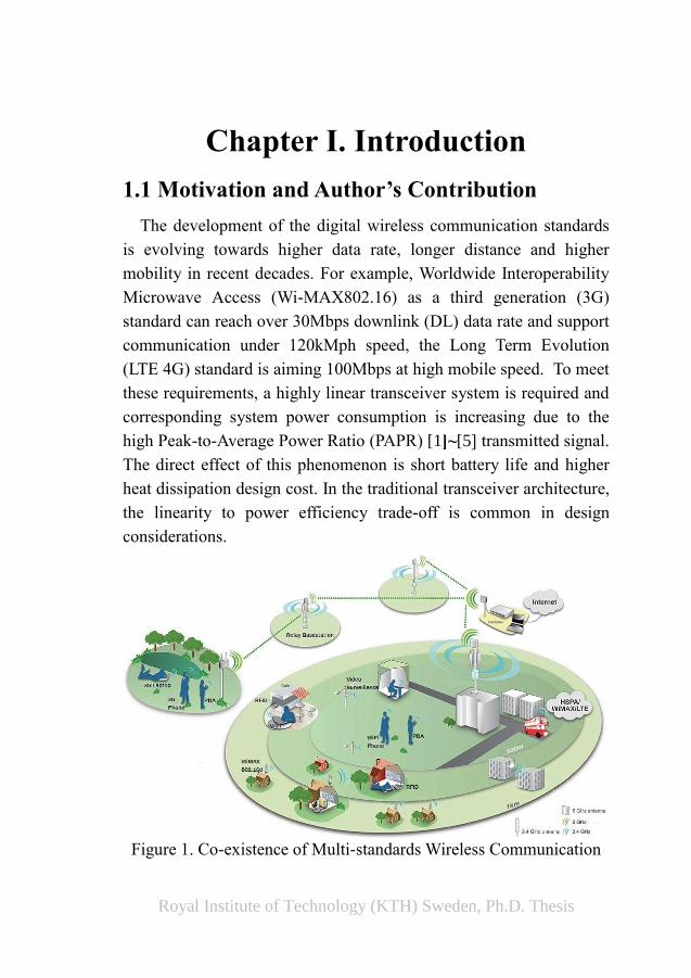
Figure 1. Co-existence of Multi-standards Wireless Communication
2 Chapter I. Introduction
Royal Institute of Technology (KTH) Sweden, Ph.D. Thesis
At the meantime, varieties of wireless communication standards
co-exist and complement each other to form a full cover of different
needs, Bluetooth WiFi and UMTS modules are basic configurations
in most CPEs. Systems like Bluetooth and WiFi may be designed in
the same chip to form Multi-Chip-Module solutions. The use of
different communication bands and time space slots increase the
efficiency of limited resources usage. To handle the smooth switching
between different standards, a fully integrated solution will have more
values in the embedded system designs, because the costs of
packaging and peripheral designs are saved. The Software Defined
Radio (SDR) concept is proposed based on this purpose and it can
provide highly adaptive system architecture for multiple
communication standards [23]~[25]. The feasibility of SDR is also
becoming higher with CMOS process scaling and more digital
functions can be realized in the same silicon area.
In this research work, the SDR transceiver architecture especially
the all-digital transmitter architecture is investigated. The comparison
between different transmitter architectures is firstly carried out to find
a suitable topology for the all-digital implementation. Secondly, after
choosing the polar architecture, an all-digital polar transmitter based
on the 90nm CMOS technology is designed. The methods to optimize
switching amplifier are developed using multiple design tools. The
linearity and power efficiency performance is measured for the low
supply voltage transmitter, the mechanism and compensation methods
for the transmitter are also investigated. Thirdly, based on the all-
digital polar transmitter architecture feature, a fully SDR RFID
transmitter is proposed, designed in hardware description language
(HDL) and verified by FPGA. This experiment proved the adaptive
feature of digital polar architecture in certain applications and pointed
out the possibility of fully SDR realization for any transmitter in the
Chapter I. Introduction 3
Royal Institute of Technology (KTH) Sweden, Ph.D. Thesis
future by using digital polar architecture.
In this thesis work, the contribution of author can be summarized
as:
1. The design and verification of the all-digital polar transmitter
from schematic to the final PCB based demo with FPGA and
computer aided measurement tools. [P3][P5][P6][P7]
2. The theoretical work on the all-digital polar transmitter
architecture and the performance under low voltage environment.
[P2][P3][P6][P8]
3. The genuine creation of the pure software RFID transmitter
prototype based on all-digital polar SDR architecture. This
experimental work extended the realm of digital polar transmitter.
[P1][P4].
The thesis work is a mixed research on the digital design
methodology for linear system involving different tools and design
levels. The verifying of all-digital polar transmitter and the
corresponding extension in RFID application proved the system can
solve linearity to efficiency conflicts, and this feature can gain
advantage from the process scaling, which provided a new design
path for future CMOS SDR system.
1.2 Thesis Research Backgrounds
1.2.1 Wireless Digital Communication Developing Trend
Modulation, Multiplexing and Duplexing. The contemporary
wireless communication is a form of art to create new dimensions in
human thinking and a technology to use limited space frequency and
energy resources more efficiently. Due to the human needs of
4 Chapter I. Introduction
Royal Institute of Technology (KTH) Sweden, Ph.D. Thesis
seamless communication, a common trend of higher data rate and
higher spectral efficiency are achieved by using complex signal
modulations. Traditional Quadrature Phase Shift Keying (QPSK)
modulation is gradually replaced by 8PSK (8 Phase Shift Keying) and
Quadrature Amplitude Modulation (QAM16 QAM 64 even QAM
256), the spectral efficiency is dramatically increased.
As the wireless communication between two objects is through air
interface media, the multiplexing methods of communication are also
developing to accommodate the trend for high data rate and using the
frequency or time window resource more efficiently. In the spectrum
(frequency) domain, communication system is developing from single
carrier (SC) system to multi-carrier (MC) system and one of the most
implemented MC systems is using Orthogonal Frequency Division
Multiplexing (OFDM) algorithm. A latest research even prototyped
the transmission based on Orbital Angular Momentum (OAM)
algorithm and reached the data rate over Terabits per second (TBPS).
In the transient domain, Time Division Multiple Access (TDMA) is
outdated by the Frequency Division Multiple Access and then Code
Division Multiple Access (CDMA) for special requirements like
Quality of Services (QoS). The use of Multiple Input Multiple Output
(MIMO) and Space Division Multiple Access (SDMA) further extend
the data rate triple or quadruple times.
The duplexing of communication system is more about how
separate systems communicate to each other. The prevailing two
schemes are Time Division Duplexing (TDD) and Frequency
Division Duplexing (FDD). Due to the limited spectral band, TDD
system is gaining more favor but both of them will co-exist for
different applications. In this case, the transceiver systems are
required to have fast switching ability and high immunity to other
Chapter I. Introduction 5
Royal Institute of Technology (KTH) Sweden, Ph.D. Thesis
interferences.
There are other parameters in the communication system like
Cyclic Redundancy Check (CRC) or system enhance methods like
Hybrid Automatic Repeat Request (HARQ) to increase the
performance but the basic mathematical description of the system is
defined by the modulation, multiplexing and duplexing parameters.
Then, the design of the transceiver system is the mapping of the
theoretical expressions into individual process blocks.
1.2.2 Transceiver Architectures
Mapping and Optimization. As the physical body to realize these
wireless communication standards, the transceiver has to fulfill the
linearity requirements to ensure signal transmitting/receiving quality.
The corresponding blocks in the transmitter/receiver chain are
required to accommodate the performance changes. Because of the
trend described above, all the parameters demand a highly linear
system in common, in both receiver and transmitter path, the cost for
linear system is the power consumption and system efficiency. For
example, the worst PAPR for WiFi (802.11g) communication is 52
(17dB) [2] [5], for a pure linear transmitter, the efficiency of the linear
power amplifier (PA) will be only 2%. It is a common scenario that
the transmitter system efficiency is lower than 10% and the figure
will be even lower for other high data rate communications.
For this reason, the system blocks need to be balanced in work load
and be efficient as a whole system. Based on this concept, the
exploration of the system architecture is the focus at the beginning of
the whole research period. Out-phasing and Polar systems are two of
the options to realize the mathematical explanation of the transmitter
6 Chapter I. Introduction
Royal Institute of Technology (KTH) Sweden, Ph.D. Thesis
system, so the comparison on these two systems with the traditional
Cartesian (direct conversion) transmitter system is made. On the other
side, more digital processing functions are emphasized to increase the
possibility of correct signal detection in the receiver system and the
SDR realization. To combine the advantages of efficiency transmitter
system topology and the digital processing algorithm, the all-digital
polar transmitter architecture is chosen as the main direction of the
thesis work.
In the system level exploration, ADS and Matlab tools are used to
simulate the signal flow and blocks performance. The simulation
results reveal the weakness and advantages of different systems, and
the optimization tool in ADS also accelerates the design progress for
the filter matching network blocks.
1.2.3 CMOS Process Features
Digital, Fast Switching and Parasitic. The most underlying
grounds for all these communication technologies are the
Complementary Metal-Oxide Semiconductor (CMOS) technology.
With the process scaling, CMOS technology is evolving towards
shorter channels, higher transition frequency, lower supplying
voltage, lower power and higher components density directions. The
direct consequence of this phenomenon is that the CMOS transistors
are acting more like on-off switching components than linear
operation ones. This feature triggered the design migration from
‘analog’ to ‘digital’ domain. More complex mathematical functions
are realized in the digital parts and more transceiver components are
designed in digital style. The ‘analog’ part of the system remains
almost same design area due to analog linearity requirements but
fewer functionality ratios of the whole system. For this reason, it is of
great value to explore the solution using all digital transceiver design
Chapter I. Introduction 7
Royal Institute of Technology (KTH) Sweden, Ph.D. Thesis
to minimize the system analog design area and increase adaptability.
With the scaling of CMOS process, even though the unit gate input
capacitance is increasing, the trans-conductance, voltage gain and unit
gain frequency is increased with shrinking channel length. For large
power switching devices, interconnection parasitic power loss will
dominant the loss, thus the driver circuits design and the whole power
amplifier efficiency needs to be optimized for certain amount of
output power. Another problem accompanying process scaling for
CMOS power devices is the effective voltage headroom. When drain
source supplying voltage is shrinking from 2.5 Volt to merely 1.0
Volt, the effective voltage is reduced further than the voltage ratio.
The voltage drop has great effect on the output voltage swing for the
power amplifiers. The channel resistance is also increased since MOS
transistors are following “alpha law” [155] instead of “square low” in
the Nano-Meter realm. So under the siege of low voltage, large output
power (large current) and channel resistance, the CMOS based
switching power amplifier design needs considerations from different
hierarchies.
1.2.4 Software Defined Radio
Flexibility and Multi-Standards. The definition of Software
Defined Radio is “A communication system implementing most
system blocks in software style and requires minimal hardware
designs” [25], in other words, SDR system is designed to use as much
baseband hardware computation resource as possible. The advantage
of using SDR is that it has minimal receiver area to handle multiple
standards. The reuse of hardware resource reduced the design cost
and provided a balanced power efficient solution for the future
wireless communication developing trends.
8 Chapter I. Introduction
Royal Institute of Technology (KTH) Sweden, Ph.D. Thesis
For the contemporary wireless communication standards, a variety of bandwidth, modulation and duplexing exists, so the specification of SDR needs to meet the most stringent requirements. In most cases, the system is featured with a high speed Analog-to-Digital Converter in the RX chain and the cost for a direct sampling ADC will need to cover a large frequency band over 6GHz. In other cases, adaptive SDR system will adjust itself for different applications and reduce power consumption when additional function is not running. In the TX chain, a cluster of transmitters for different bands with power combination module will be used. The flexibility is realized both with configurable hardware modules and digital control algorithms.
1.3 Problem Description of the Research Work
Based on the previous introduction on the wireless communication developing trend, transceiver architecture and CMOS process features, the main problems which this thesis work trying to solve are listed below:
1. Which transmitter ARCHITECTURE can be the most suitable one to accommodate the developing trend of current wireless communication standards and provide a balanced solution to the linearity to power efficiency trade-offs.
2. Based on the CMOS process scaling feature, can we take the advantage of the CMOS switching characteristics and to what extent can we find a digital design METHODOLOGY / ALGORITHM for the transmitter system design.
3. Based on the answer of previous two problems, how to realize a SDR SOLUTION and maximally keep the advantages gained by mapping the system into mostly digital process even into a program.
There are also other problems need to be solved before finding

Chapter I. Introduction 9
Royal Institute of Technology (KTH) Sweden, Ph.D. Thesis
answers to these three questions. For example, the engineering work
like PCB design and measurement equipment operation to capture the
data successfully, the use of different software tools to accelerate the
design and to process the data to find rules. The most important thing
in the research work is to keep an open mind and make full use of
what you have learned and make a combined creation based on
current technology and resources.
Communication
StandardsEDA Tools Design Process
System
Architecture
Circuit
Topology
Instrument
Operation
Design for Test
Experience
Circuit Design
SkillTesting Skill
Successful
Design
Figure 2. The Pyramid of System Design
! STEP 1: Process Design Kits & Design Tools Fixed Down.
! STEP 2: Knowing and Understanding the Interface Parameters.
! STEP 3: System Architecture Investigation and Fixed Down.
! STEP 4: System Level Simulation and Block Partition.
! STEP 5: Circuit Design and Simulation.
! STEP 6: Layout and Post-layout Simulation.
! STEP 7: Packaging Design.
! STEP 8: Test Board Design and Instrument Configuration.
! STEP 9: Measurement and Optimization.
A general summarization based on personal experience is drawn in
Figure 2 for illustration. The corresponding steps are listed below. It
provides a general view for the whole system design process and
thinking ahead of the steps will gain you more chance for a successful
design.
10 Chapter I. Introduction
Royal Institute of Technology (KTH) Sweden, Ph.D. Thesis
1.4 Thesis Outline
The following contents of this thesis are arranged in a top-down
hierarchical style.
In Chapter II, the SDR system architecture will be explained and
the partition of analog and digital part will be briefly estimated. The
contemporary wireless communication standards examples are listed
and the key parameters for transceiver design will be extracted. As the
key part of SDR TX chain, the transmitter architecture investigation
and simulation will be analyzed and comparison will be made
between different options. In the RX chain, as the bridge between RF
analog and digital blocks, the analog to digital converter will be
introduced. A fixed down of SDR system architecture will be done as
the answer to the first question.
In Chapter III, to maximize the use of digital process and
algorithm, the modification on the transmitter blocks will be done and
the blocks design work from schematic to layout will be presented.
The measurement results for the transmitter will be examined to
evaluate the linearity and efficiency. This part of work will also give
the answers to the second question.
In Chapter IV, to further realize a universal SDR architecture based
on the design in previous chapter, it is of great value to optimize the
system for certain applications like RFID and evaluate the possibility
for fully SDR realization. In other words, check how the system can
be designed in software and program into devices for different
applications. And what are the basic hardware requirements for this
hardware to software conversion. In Chapter V, the conclusions and
summary of the complete work will be presented.
Chapter I. Introduction 11
Royal Institute of Technology (KTH) Sweden, Ph.D. Thesis
1.5 Publication List and Author’s Contribution
The listed publications are the academic contribution during the
research works. They provided the landmark for the whole research
period and also point out the future developing direction.
In publication P1 – "Systematic Design of a Flash ADC for UWB
Applications", the author is aiming to provide a universal interface for
the SDR receiver chain for different wireless standards. This paper
presents the systematic design of a 5-bit, 1.2 GSPS interpolative flash
ADC for multiband OFDM UWB applications. The proposed ADC
architecture employs the proven capacitive interpolation, which
greatly reduce the power consumption, by eliminating the need of a
power hungry resistive ladder. The flash ADC has been implemented
in a 0.18 um CMOS process. Circuit level simulations show that the
proposed architecture can achieve an SNDR of 25.3 dB, and an SFDR
of 29.3 dB, with an input signal frequency of 330 MHz, at a sampling
rate of 1.2 GSPS. The ADC core dissipates 130 mW from a 1.8 V
supply.
The contribution of the author is the investigation of ADC
topologies for SDR architecture. The design from system level to
circuit level of the selected interpolative Flash ADC and the writing
of the manuscript is done by the author. Matlab modeling and
Cadence simulation/layout is carried out in this work to verify the
interpolative switching capacitance ADC. The article is submitted by
Dr. Martin Gustafsson in 2007.
In publication P2 – “RF Transmitter Architecture Investigation for
Power Efficient Mobile WiMAX Applications”, out-phasing (LINC)
and polar transmitter architectures are investigated and compared
with direct conversion (DC) architecture. Complete system solution
12 Chapter I. Introduction
Royal Institute of Technology (KTH) Sweden, Ph.D. Thesis
targeting 23dBm output power is evaluated. System level simulation
result shows that, with linear power combiner, LINC consumes more
power than DC if non-clipping modulation scheme used. And polar
system has stringent 3 degree phase matching and 0.5dB gain
matching requirements to meet EVM and spectrum mask
specifications.
The contribution of the author is the system level comparison of 3
different transmitter architectures and the extraction of power
amplifier parameters for WiMAX transmitters. The author also wrote
the manuscript for the publication. ADS simulation and system
manipulation work is carried out by the author in this period to
investigate the performance tradeoffs between different architectures.
In publication P3 – “A switch mode resonating H-Bridge polar
transmitter using RF ΣΔ modulation” is the result of circuit level
design, a polar transmitter using H-Bridge configured Class-D
amplifiers is proposed. To fully utilize low voltage resource, maintain
linearity and meet the spectrum mask requirements, RF Low Pass
Sigma-Delta Modulation (LPSDM) is used. An on-chip transformer
based filter network is designed to filter out SDM noise and provide
load matching. The system verification is carried out by using Matlab
passband simulation on a 13dB PAR mobile WiMAX signal.
Evaluation of noise shaping and spectral regrowth shows the
proposed architecture can achieve -45dBc/10kHz ACPR in a 140MHz
bandwidth range. This provides a solid ground for the circuit design
work.
The author contributes to the architecture selection, modification
and system level simulation of the proposed digital polar transmitter
architecture and the prepared further implementation of the
Chapter I. Introduction 13
Royal Institute of Technology (KTH) Sweden, Ph.D. Thesis
transmitter system like required PLL phase noise level and
bandwidth. The manuscript is also finished by the author. Matlab
simulation is carried out with technical support from Catena Wireless
AB.
In publication P4 – “A Polar Transmitter Architecture with Digital
Switching Amplifier for UHF RFID Applications”, an all-digital polar
transmitter is proposed and verified by transient signal analysis and
random pattern simulation. The timing and signal quality constraints
of the digital polar transmitter circuits are extracted. Due to the use of
RF frequency low pass sigma delta modulation, the system can be
designed in pure digital process without on-chip inductive
components. Compared to the 31% theoretical efficiency by using
class-A linear power amplifier, a minimum 77% theoretical efficiency
can be achieved in this proposed digital RFID system.
The contribution of the author is the simulation and design of the
genuine prototype of SDR UHF RFID transmitter. The transmitter is
programmed into FPGA for verification and the manuscript is written
by the author. Matlab and VHDL design is carried out by the author
alone.
In publication P5 – "All-digital transmitter based on ADPLL and
phase synchronized delta sigma modulator", A novel architecture of
all-digital polar transmitters is proposed, mainly composed of an all-
digital PLL (ADPLL) for phase modulation, a 1-bit low-pass delta
sigma modulator for envelop modulation and a high efficiency class-
D PA. The low noise ADPLL and high oversample Sigma Delta
modulator relax filter design, enabling the use of an on-chip filter.
The differential signaling scheme enhances the power of the
fundamental tone and suppresses DC and high harmonics. The
14 Chapter I. Introduction
Royal Institute of Technology (KTH) Sweden, Ph.D. Thesis
transmitter was fabricated in a 90nm digital CMOS process,
occupying 1.4 mm2. The measurement results demonstrate
effectiveness of the architecture. The digital transmitter consumes 58
mW from a 1 V supply, delivering a 6.81-dBm output.
The contribution of the author in this article is the system
architecture verification, the partition of the system and the block
parameters extraction. Transmitter output measurement results and
the first draft are provided by the author. My colleague Jian Chen is
working on the all-digital PLL design. The measurement of the PA
part is carried out by the author and the whole system measurement is
carried out by both authors of the article.
In publication P6 – "A 11.4dBm 90nm CMOS H-Bridge
resonating polar amplifier using RF Sigma Delta Modulation", the
author improved the measurement skill and applied optimization
methods to the amplifier, measurement results are concluded on the
digital polar transmitter. The experimental results from lab
measurement with real physical design verify the initial concept and
also revealed the possible improvements for future works.
The contributions of the author are the optimization of the all-
digital polar transmitter/amplifier and the measurement and
processing of the results. The manuscript is written by the author.
During the measurement, features of the H-Bridge CMOS amplifier is
explored and FPGA/Virtual instrument measurement skills are
developed by the author.
In publication P7 – "The Design of All-Digital Polar Transmitter
Based on ADPLL and Phase Synchronized ΣΔ Modulator”, as a
summary and collaboration, the publication completes the whole
Chapter I. Introduction 15
Royal Institute of Technology (KTH) Sweden, Ph.D. Thesis
thesis work and also proved the value of the research work. The
complete solution described in the journal publication setup a good
reference for further developing in this area.
The contributions of the author are the providing of transmitter
optimized power output measurement results, constellation
measurement results and draft of the paper since this work is a
promoted article from publication P5.
In publication P8 - “High Efficiency RF Transmitter System
Architecture Investigation for Mobile WiMAX Applications”, the
author started his research on the transmitter architecture and it is
carried out in the industry company. This period work provided first
insight of the future advanced wireless communication standards and
setup the direction of future research work.
The contribution of the author in this work is the investigation of
complex modulation and multiplexing system transmitter
requirements. The author fixed down the system partitioned blocks
parameters especially the transmitter requirements and wrote the
manuscript based on this period of research. This work is carried out
with the technical support and cooperation with Catena Wireless AB.

16 Chapter I. Introduction
Royal Institute of Technology (KTH) Sweden, Ph.D. Thesis
(This page is intentionally left blank.)
Royal Institute of Technology (KTH) Sweden, Ph.D. Thesis
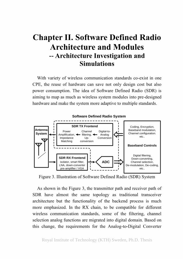
Chapter II. Software Defined Radio
Architecture and Modules -- Architecture Investigation and
Simulations
With variety of wireless communication standards co-exist in one
CPE, the reuse of hardware can save not only design cost but also
power consumption. The idea of Software Defined Radio (SDR) is
aiming to map as much as wireless system modules into pre-designed
hardware and make the system more adaptive to multiple standards.
Coding, Encryption,
Baseband modulation,
Channel configuration.
etc..
SDR RX Frontend
Software Defined Radio System
Baseband Controls
isolator, smart filter,
LNA, down-converter
pre-amplifier / VGA
ADC
Antenna
System
Digital filtering,
Down-converting,
Channel selection,
De-modulation, De-coding,
etc..
SDR TX Frontend
Digital-to-
Analog
Conversion
Channel
filtering,
Up-
conversion
Power
Amplification,
Impedance
Matching
Figure 3. Illustration of Software Defined Radio (SDR) System
As shown in the Figure 3, the transmitter path and receiver path of
SDR have almost the same topology as traditional transceiver
architecture but the functionality of the backend process is much
more emphasized. In the RX chain, to be compatible for different
wireless communication standards, some of the filtering, channel
selection analog functions are migrated into digital domain. Based on
this change, the requirements for the Analog-to-Digital Converter
18 Chapter II. Software Defined Radio Architecture and Modules
Royal Institute of Technology (KTH) Sweden, Ph.D. Thesis
(ADC) are increased on the resolution, sampling rate and full scale
range aspects to cover the largest bandwidth, the largest dynamic
range inputs among all the received signals. In the TX chain, to
generate the corresponding signal, a high speed large resolution
Digital-to-Analog Converter is also needed and the up-converter will
be required to have 100MHz to 3GHz up-conversion range. The
power amplifier of the transmitter will also be adapted for this large
frequency range.
In order to make the whole system work, the SDR system is not
only required to have a powerful backend processing capability but
also a balanced front end design. Multi-chip Modules (MCM)
solutions are mostly accepted with programmable center controlling
unit [24] and the research on integrated solution is still on-going.
2.1 Wireless Communication Standards
Although the modern digital communication system has the trend
of expanding bandwidth, the available frequency band is remaining
the same for decades since the introduction of the first generation
(1G) wireless communication in the early 1980s. Due to the scarce of
spectrum resource, complex spectrum efficient modulation and
multiplexing algorithms are developed. A summarized table (Table 1)
is presented below for the explanation of the developing trend.
The pursing of high date rate has pushed wireless communication
system to use QAM64 and OFDM-1024 technique and error
correction algorithms, the advantages of using these advanced
communication systems are:
Higher spectrum efficiency of up to 16bps/Hz.
Robustness to multipath fading and interference.
Support large number of users by scalable channel usage.
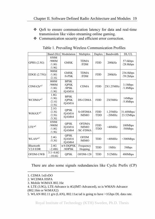
Chapter II. Software Defined Radio Architecture and Modules 19
Royal Institute of Technology (KTH) Sweden, Ph.D. Thesis
QoS to ensure communication latency for data and real-time
transmission like video streaming online gaming.
Communication security and efficient error correction.
Table 1. Prevailing Wireless Communication Profiles
Band (Hz) Modulation Multiplex Duplex Bandwidth DL/UL
GPRS (2.5G)
850M
/900M
/1.8G
/1.9G
GMSK TDMA
/FDM FDD 200kHz
57.6kbps
/28.8kbps
EDGE (2.75G)
900M
/1.8G
/2.1G
GMSK
/8-PSK
TDMA
/FDM FDD 200kHz
236.8kbps
/59.2kbps
CDMA2k*1
800M
/900M
/1.8G
/1.9G
BPSK
/QPSK
/8PSK
/QAM16
CDMA FDD 2X1.25MHz 3.1Mbps
/1.8Mbps
WCDMA*2
1.8G
/1.9G
/2.1G
/2.5G
BPSK
/QPSK
/QAM16
DS-CDMA FDD 2X5MHz 14Mbps
/5.8Mbps
WiMAX*3
2.1G
/2.3G
/2.5G
/3.3G
QPSK
/QAM16
/QAM64
S-OFDMA
/MIMO
FDD
/TDD
1.25MHz
~20MHz
31.68Mbps/
23.52Mbps
LTE*4
850M
/900M
/1.8G
/1.9G
QPSK
/QAM16
/QAM64
OFDMA
/MIMO
/SC-FDMA
FDD
/TDD <40MHz
100Mbps
/50Mbps
WLAN*5 2.4G
/5.3G
QPSK
/QAM16
/QAM64
OFDM
/MIMO TDD <40MHz <300Mbps
Bluetooth
V2.0 EDR
2.4G
~2.48G
π/4-DQPSK
/8DPSK
Frequency
Hopping TDD 1MHz 3Mbps
OFDM-UWB 3.1~4.6G
~10.6G QPSK OFDM-128 TDD 512MHz 480Mbps
There are also some signals redundancies like Cyclic Prefix (CP)
1. CDMA 1xEvDO
2. WCDMA HSPA
3. Mobile WiMAX 802.16e
4. LTE (3.9G), LTE-Advance is 4G(IMT-Advanced), so is WMAN-Advance
(802.16m or WiMAX2)
5. WLAN 802.11 g/n (LAN), 802.11ac/ad is going to have >1Gbps DL data rate.
20 Chapter II. Software Defined Radio Architecture and Modules
Royal Institute of Technology (KTH) Sweden, Ph.D. Thesis
and Coding Rate (CR) exist in the transmission. They are data
packaging parameters in the baseband signal processing. The main
front-end design parameters like modulation and multiplexing are the
focus of this thesis work and these are the parameters defining the
transmitted signal characteristics.
2.1.1 Wireless Communication Air Interface Example
To identify the general requirements for SDR transmitter
application, the WiMAX (IEEE 802.16e) standard is used here as an
example. The parameters defined are quite representative for future
wireless communication based on the developing trend.
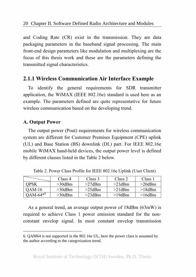
A. Output Power
The output power (Pout) requirements for wireless communication
system are different for Customer Premises Equipment (CPE) uplink
(UL) and Base Station (BS) downlink (DL) part. For IEEE 802.16e
mobile WiMAX hand-held devices, the output power level is defined
by different classes listed in the Table 2 below.
Table 2. Power Class Profile for IEEE 802.16e Uplink (User Client)
Class 4 Class 3 Class 2 Class 1
QPSK >30dBm >27dBm >23dBm >20dBm
QAM-16 >30dBm >25dBm >21dBm >18dBm
QAM-64*6 >30dBm >23dBm >19dBm >16dBm
As a general trend, an average output power of 18dBm (63mW) is
required to achieve Class 1 power emission standard for the non-
constant envelop signal. In most constant envelop transmission
6. QAM64 is not supported in the 802.16e UL, here the power class is assumed by
the author according to the categorization trend.
Chapter II. Software Defined Radio Architecture and Modules 21
Royal Institute of Technology (KTH) Sweden, Ph.D. Thesis
standards like GSM or EDGE, the required average output power will
be over 30dBm (1W), which is quite a high power comparing with
short range wireless communication.
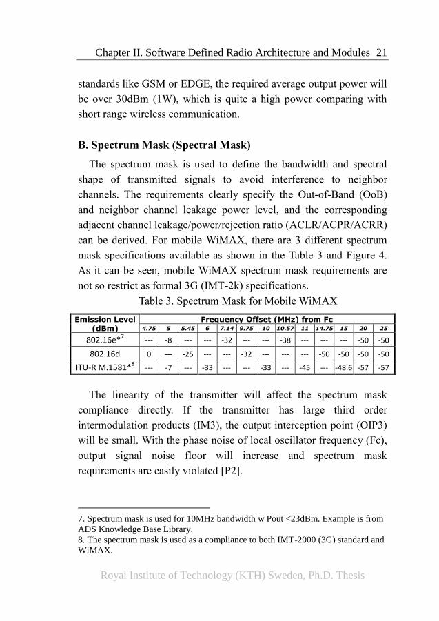
B. Spectrum Mask (Spectral Mask)
The spectrum mask is used to define the bandwidth and spectral
shape of transmitted signals to avoid interference to neighbor
channels. The requirements clearly specify the Out-of-Band (OoB)
and neighbor channel leakage power level, and the corresponding
adjacent channel leakage/power/rejection ratio (ACLR/ACPR/ACRR)
can be derived. For mobile WiMAX, there are 3 different spectrum
mask specifications available as shown in the Table 3 and Figure 4.
As it can be seen, mobile WiMAX spectrum mask requirements are
not so restrict as formal 3G (IMT-2k) specifications.
Table 3. Spectrum Mask for Mobile WiMAX
Emission Level (dBm)
Frequency Offset (MHz) from Fc 4.75 5 5.45 6 7.14 9.75 10 10.57 11 14.75 15 20 25
802.16e*7 --- -8 --- --- -32 --- --- -38 --- --- --- -50 -50
802.16d 0 --- -25 --- --- -32 --- --- --- -50 -50 -50 -50
ITU-R M.1581*8 --- -7 --- -33 --- --- -33 --- -45 --- -48.6 -57 -57
The linearity of the transmitter will affect the spectrum mask
compliance directly. If the transmitter has large third order
intermodulation products (IM3), the output interception point (OIP3)
will be small. With the phase noise of local oscillator frequency (Fc),
output signal noise floor will increase and spectrum mask
requirements are easily violated [P2].
7. Spectrum mask is used for 10MHz bandwidth w Pout <23dBm. Example is from
ADS Knowledge Base Library.
8. The spectrum mask is used as a compliance to both IMT-2000 (3G) standard and
WiMAX.
22 Chapter II. Software Defined Radio Architecture and Modules
Royal Institute of Technology (KTH) Sweden, Ph.D. Thesis
Figure 4. WiMAX Spectrum Mask Illustration
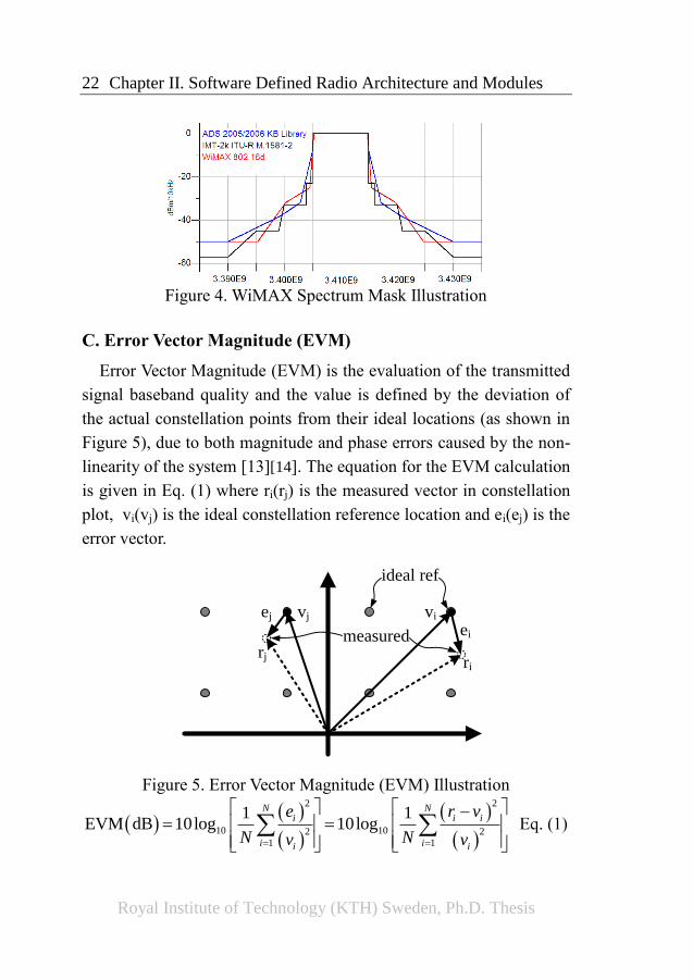
C. Error Vector Magnitude (EVM)
Error Vector Magnitude (EVM) is the evaluation of the transmitted
signal baseband quality and the value is defined by the deviation of
the actual constellation points from their ideal locations (as shown in
Figure 5), due to both magnitude and phase errors caused by the non-
linearity of the system [13][14]. The equation for the EVM calculation
is given in Eq. (1) where ri(rj) is the measured vector in constellation
plot, vi(vj) is the ideal constellation reference location and ei(ej) is the
error vector.
vi
ri
ei
ej vj
rj
ideal ref
measured
Figure 5. Error Vector Magnitude (EVM) Illustration
2 2
10 102 2
1 1
1 1EVM dB 10log 10log
N Ni i i
i ii i
e r v
N Nv v
Eq. (1)
Chapter II. Software Defined Radio Architecture and Modules 23
Royal Institute of Technology (KTH) Sweden, Ph.D. Thesis
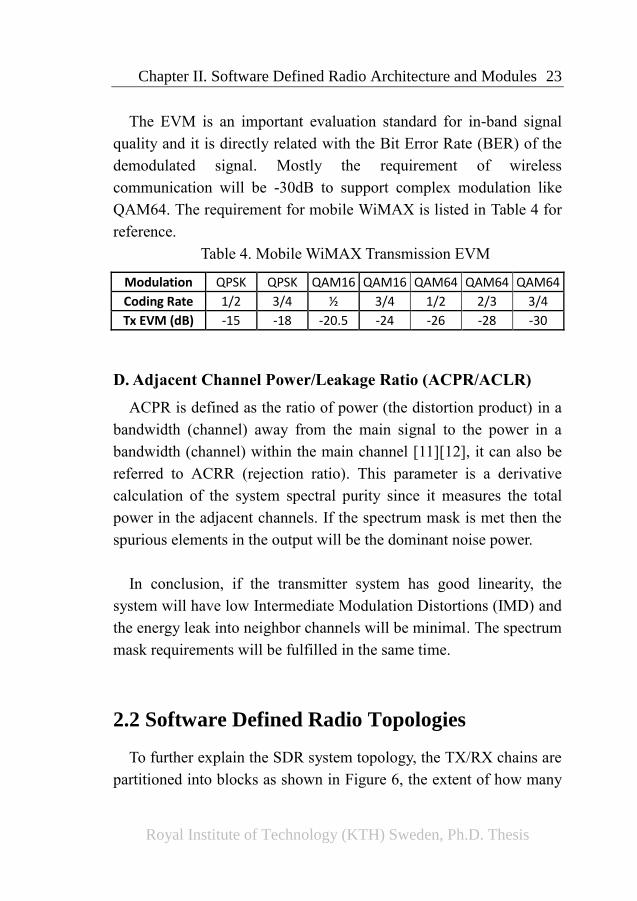
The EVM is an important evaluation standard for in-band signal
quality and it is directly related with the Bit Error Rate (BER) of the
demodulated signal. Mostly the requirement of wireless
communication will be -30dB to support complex modulation like
QAM64. The requirement for mobile WiMAX is listed in Table 4 for
reference.
Table 4. Mobile WiMAX Transmission EVM
Modulation QPSK QPSK QAM16 QAM16 QAM64 QAM64 QAM64
Coding Rate 1/2 3/4 ½ 3/4 1/2 2/3 3/4
Tx EVM (dB) -15 -18 -20.5 -24 -26 -28 -30
D. Adjacent Channel Power/Leakage Ratio (ACPR/ACLR)
ACPR is defined as the ratio of power (the distortion product) in a
bandwidth (channel) away from the main signal to the power in a
bandwidth (channel) within the main channel [11][12], it can also be
referred to ACRR (rejection ratio). This parameter is a derivative
calculation of the system spectral purity since it measures the total
power in the adjacent channels. If the spectrum mask is met then the
spurious elements in the output will be the dominant noise power.
In conclusion, if the transmitter system has good linearity, the
system will have low Intermediate Modulation Distortions (IMD) and
the energy leak into neighbor channels will be minimal. The spectrum
mask requirements will be fulfilled in the same time.
2.2 Software Defined Radio Topologies
To further explain the SDR system topology, the TX/RX chains are
partitioned into blocks as shown in Figure 6, the extent of how many
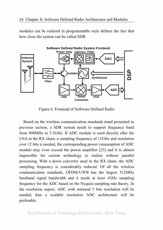
24 Chapter II. Software Defined Radio Architecture and Modules
Royal Institute of Technology (KTH) Sweden, Ph.D. Thesis
modules can be realized in programmable style defines the fact that
how close the system can be called SDR.
Software Defined Radio System Frontend
ADC
Antenna
System
DS
P
DAC
Power Amp
isolator
LNA
Filter
synthesizer
Down
Converter
UpConv. Filter
VGA
Figure 6. Frontend of Software Defined Radio
Based on the wireless communication standards trend presented in
previous section, a SDR system needs to support frequency band
from 800MHz to 5.3GHz. If ADC module is used directly after the
LNA in the RX chain, a sampling frequency of 11GHz and resolution
over 12 bits is needed, the corresponding power consumption of ADC
module may even exceed the power amplifier [23] and it is almost
impossible for current technology to realize without parallel
processing. With a down converter used in the RX chain, the ADC
sampling frequency is considerably reduced. Of all the wireless
communication standards, OFDM-UWB has the largest 512MHz
baseband signal bandwidth and it needs at least 1GHz sampling
frequency for the ADC based on the Nyquist sampling rate theory. In
the resolution aspect, ADC with minimal 5 bits resolution will be
needed, thus a scalable resolution ADC architecture will be
preferable.
Chapter II. Software Defined Radio Architecture and Modules 25
Royal Institute of Technology (KTH) Sweden, Ph.D. Thesis
In the TX chain, if a Cartesian In-phase Quadrature architecture is
adopted, traditional linear power amplifier will be mostly used to
increase the power level. The blocks after DAC will always use
analog/RF design methodologies so the SDR concept is constrained
by this limit in the TX chain.
In recent years, the research on direct RF concept [88] [95] [129] is
raised, high speed DAC is used and generate RF signal with digital
style, these experiments are very important in the SDR system
development and also provide new thoughts. In later chapters, the TX
chain design will be further explored in the thesis work.
2.3 Analog-to-Digital Converters in SDR RX
Chain
To meet different wireless communications requirements, the SDR
RX ADC for future multi-standard wireless communication should
have features as:
High speed sampling rate to cover different bandwidth even
carrier frequency.
Large resolution and adaptive output bits for different
applications.
Configuration architecture and dynamic power saving.
Linear and scalable under CMOS process.
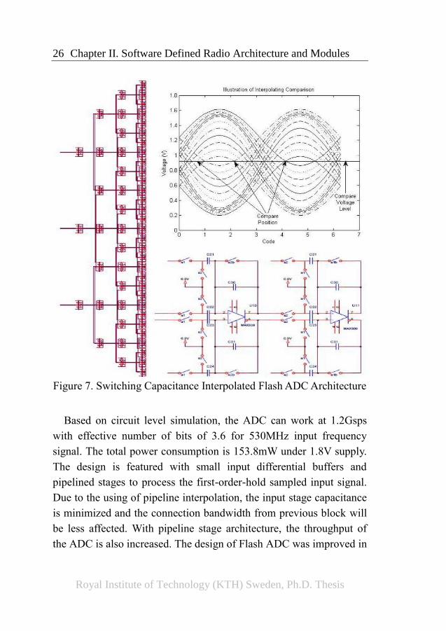
In the [P1], a switching capacitance interpolated flash ADC is
modeled and simulated at system level. To cover 512MHz baseband
bandwidth, 1.2GHz sampling frequency is used and 5-stage scalable
architecture is adopted, the ADC is designed in 180nm process and
the topology of the Flash ADC is shown in Figure 7.
26 Chapter II. Software Defined Radio Architecture and Modules
Royal Institute of Technology (KTH) Sweden, Ph.D. Thesis
Figure 7. Switching Capacitance Interpolated Flash ADC Architecture
Based on circuit level simulation, the ADC can work at 1.2Gsps
with effective number of bits of 3.6 for 530MHz input frequency
signal. The total power consumption is 153.8mW under 1.8V supply.
The design is featured with small input differential buffers and
pipelined stages to process the first-order-hold sampled input signal.
Due to the using of pipeline interpolation, the input stage capacitance
is minimized and the connection bandwidth from previous block will
be less affected. With pipeline stage architecture, the throughput of
the ADC is also increased. The design of Flash ADC was improved in
Chapter II. Software Defined Radio Architecture and Modules 27
Royal Institute of Technology (KTH) Sweden, Ph.D. Thesis
[28] which can provide configurable output bits for different
application. Extra stages of the interpolation Flash ADC can be
disabled so the power efficiency performance is enhanced.
In order to enable the SDR RX chain support 900MHz band and
process multi-standard signal, the ADC sampling rate needs to be
further raised to 2GHz under 90nm CMOS process. Under close field
communication like RFID, the LNA may amplify received signal to
detectable range for the ADC and thus the down converter can be
removed. The on-off keying envelope modulation used in the UHF
RFID specification also require lower resolution and a more complete
SDR system can be realized.
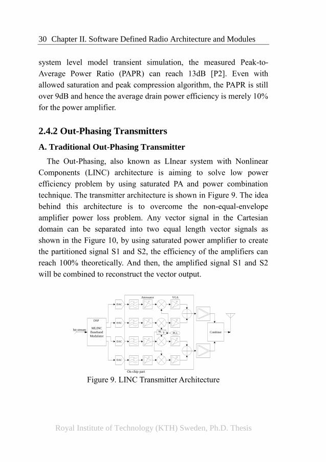
2.4 Transmitter Architecture Selection in SDR
TX Chain
In current prevailing transmitter design, three different
architectures are mostly seen. They are Cartesian In-phase Quadrature
modulation Direct Conversion, Out-Phasing (Linear System with
Non-linear Components, LINC), and Polar Modulation architectures.
The hierarchical design of transmitter systems follows the same
procedures from system model simulation to the circuit design and
verification. Firstly, partition of the system and functionality mapping
to corresponding blocks. Secondly, system level optimization and
signal node parameter calculation. Thirdly, block design parameter
calculation from known signal requirements.
During these design steps, the knowledge of EDA tool and the
process characteristics is very helpful to the designer, a simplified
28 Chapter II. Software Defined Radio Architecture and Modules
Royal Institute of Technology (KTH) Sweden, Ph.D. Thesis
model can enable the designer to make correct choice and shorten the
verification time.
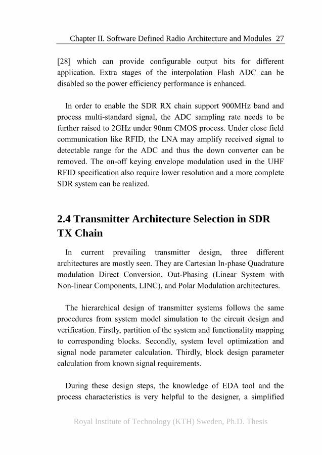
2.4.1 Direct Conversion Transmitters
As the most vastly used transmitter architecture in wireless
communication system, Direct Conversion (DC) transmitter is very
concise in topology comparing to out-phasing and polar architecture.
And it usually has minimal chip design area based on the assumption
that the blocks are same in other designs. The system architecture
illustration is shown in Figure 8.
Direct
Conversion
Baseband
DAC
Attenuator VGA
On chip part
DSP
DAC
PLL 900
PA
Figure 8. Direct Conversion Architecture
In the DC system baseband, Cartesian modulation is used and In-
phase / Quadrature signals are generated. Since the IQ modulation is
realized by digital processing, two digital-to-analog converts (DAC)
are used. After the DACs, low-pass filters (LPF) are used to remove
the harmonics caused by zero-order holder style output signal from
the DAC. Attenuators are used to adjust the signal swing amplitude to
ensure the mixer is working at the best input bias, after the mixer,
baseband signal is up-converted to RF frequency. Then the signal will
be adjusted by RF-VGA and combined to create the final RF output
signal.
Due to the process limitation, the IQ signal combiner output power
level is still small and normally it is in the range of -1dBm to 3dBm.
In order to achieve required 23dBm average output power, a discrete
Chapter II. Software Defined Radio Architecture and Modules 29
Royal Institute of Technology (KTH) Sweden, Ph.D. Thesis
Power Amplifier (PA) is used in most designs. The use of discrete PA
brings the system disadvantages as below.
Different voltage domain and extra discrete components cost
for PCB integration.
Matching of RF transmission trace and power noise isolation
problems.
Power waste and thermal problems.
The discrete PA using BiCMOS or SiGe process is much expensive
than integrated CMOS solution and the most critical drawback is the
power waste of the linear PA. For future WiMAX or LTE system with
QAM64 and OFDM-1024, the calculation of peak output signal
voltage is based on transient response of IFFT conversion signal from
Eq. (2) listed below.
( 1)/2 ( 1)/2 ( 1)/2, ~
2 ( ) 2 ( )
max ,
( 1)/2, 0 ( 1)/2, 0 ( 1)/2, 0
max Re sc CP sc CP
k N n N m N m nj k f t T j m f t T
k m n i j
k N k n N n m N m
y C e M C C e
Eq. (2)
Here N present the number of subcarriers, f0 is the center carrier
frequency of RF signal, Tcp is the time of Cyclic Prefix (CP) time to
avoid Inter Symbol Interference (ISI) during transmission, Δfsc is the
frequency space for each subcarrier in the band. M is the mutual
product coefficient of two subcarrier signals.
This equation presents that the peak value is dominated by the
carrier number as well as the inter-modulation coefficient of the linear
PA. For example, there are 720 data sub-carriers, 184 null sub-carriers
and 120 pilot sub-carriers exist in the mobile WiMAX OFDM-1024
system, the effective number is 840 for N. Based on this equation and
30 Chapter II. Software Defined Radio Architecture and Modules
Royal Institute of Technology (KTH) Sweden, Ph.D. Thesis
system level model transient simulation, the measured Peak-to-
Average Power Ratio (PAPR) can reach 13dB [P2]. Even with
allowed saturation and peak compression algorithm, the PAPR is still
over 9dB and hence the average drain power efficiency is merely 10%
for the power amplifier.
2.4.2 Out-Phasing Transmitters
A. Traditional Out-Phasing Transmitter
The Out-Phasing, also known as LInear system with Nonlinear
Components (LINC) architecture is aiming to solve low power
efficiency problem by using saturated PA and power combination
technique. The transmitter architecture is shown in Figure 9. The idea
behind this architecture is to overcome the non-equal-envelope
amplifier power loss problem. Any vector signal in the Cartesian
domain can be separated into two equal length vector signals as
shown in the Figure 10, by using saturated power amplifier to create
the partitioned signal S1 and S2, the efficiency of the amplifiers can
reach 100% theoretically. And then, the amplified signal S1 and S2
will be combined to reconstruct the vector output.
bit streamMLINC
Baseband
Modulator
DAC
Attenuator VGA
On chip part
DSP
Combiner
DAC
DAC
DAC
PLL90 0
Figure 9. LINC Transmitter Architecture
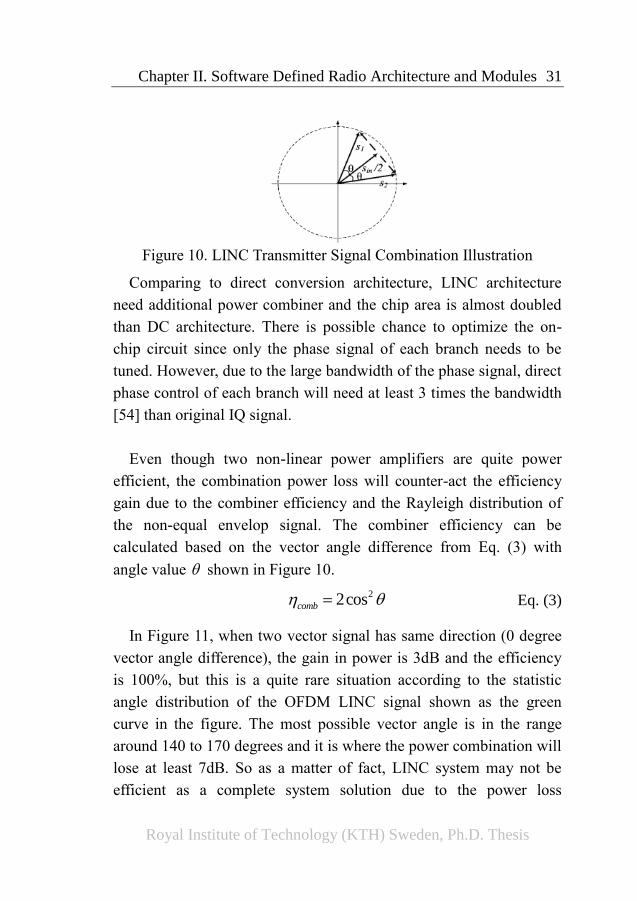
Chapter II. Software Defined Radio Architecture and Modules 31
Royal Institute of Technology (KTH) Sweden, Ph.D. Thesis
Figure 10. LINC Transmitter Signal Combination Illustration
Comparing to direct conversion architecture, LINC architecture
need additional power combiner and the chip area is almost doubled
than DC architecture. There is possible chance to optimize the on-
chip circuit since only the phase signal of each branch needs to be
tuned. However, due to the large bandwidth of the phase signal, direct
phase control of each branch will need at least 3 times the bandwidth
[54] than original IQ signal.
Even though two non-linear power amplifiers are quite power
efficient, the combination power loss will counter-act the efficiency
gain due to the combiner efficiency and the Rayleigh distribution of
the non-equal envelop signal. The combiner efficiency can be
calculated based on the vector angle difference from Eq. (3) with
angle value shown in Figure 10.
22coscomb Eq. (3)
In Figure 11, when two vector signal has same direction (0 degree
vector angle difference), the gain in power is 3dB and the efficiency
is 100%, but this is a quite rare situation according to the statistic
angle distribution of the OFDM LINC signal shown as the green
curve in the figure. The most possible vector angle is in the range
around 140 to 170 degrees and it is where the power combination will
lose at least 7dB. So as a matter of fact, LINC system may not be
efficient as a complete system solution due to the power loss
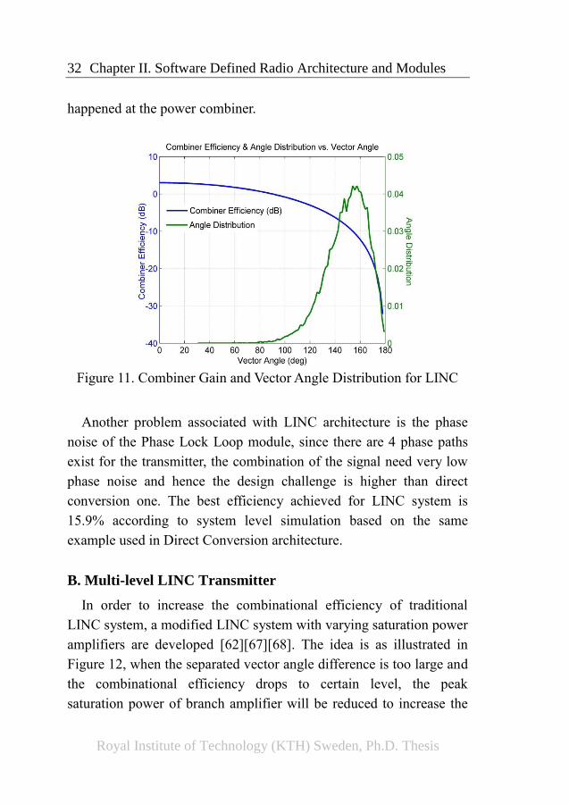
32 Chapter II. Software Defined Radio Architecture and Modules
Royal Institute of Technology (KTH) Sweden, Ph.D. Thesis
happened at the power combiner.
Figure 11. Combiner Gain and Vector Angle Distribution for LINC
Another problem associated with LINC architecture is the phase
noise of the Phase Lock Loop module, since there are 4 phase paths
exist for the transmitter, the combination of the signal need very low
phase noise and hence the design challenge is higher than direct
conversion one. The best efficiency achieved for LINC system is
15.9% according to system level simulation based on the same
example used in Direct Conversion architecture.
B. Multi-level LINC Transmitter
In order to increase the combinational efficiency of traditional
LINC system, a modified LINC system with varying saturation power
amplifiers are developed [62][67][68]. The idea is as illustrated in
Figure 12, when the separated vector angle difference is too large and
the combinational efficiency drops to certain level, the peak
saturation power of branch amplifier will be reduced to increase the
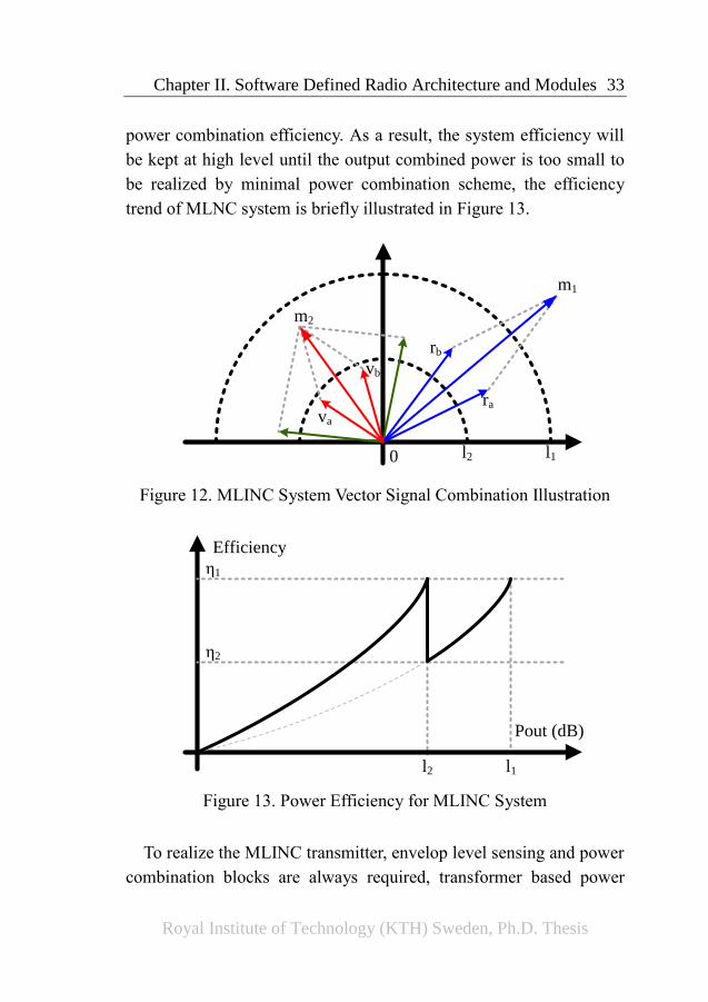
Chapter II. Software Defined Radio Architecture and Modules 33
Royal Institute of Technology (KTH) Sweden, Ph.D. Thesis
power combination efficiency. As a result, the system efficiency will
be kept at high level until the output combined power is too small to
be realized by minimal power combination scheme, the efficiency
trend of MLNC system is briefly illustrated in Figure 13.
m1
m2
l1l2
ra
rb
vb
va
0
Figure 12. MLINC System Vector Signal Combination Illustration
l1l2
Efficiency
Pout (dB)
η1
η2
Figure 13. Power Efficiency for MLINC System
To realize the MLINC transmitter, envelop level sensing and power
combination blocks are always required, transformer based power
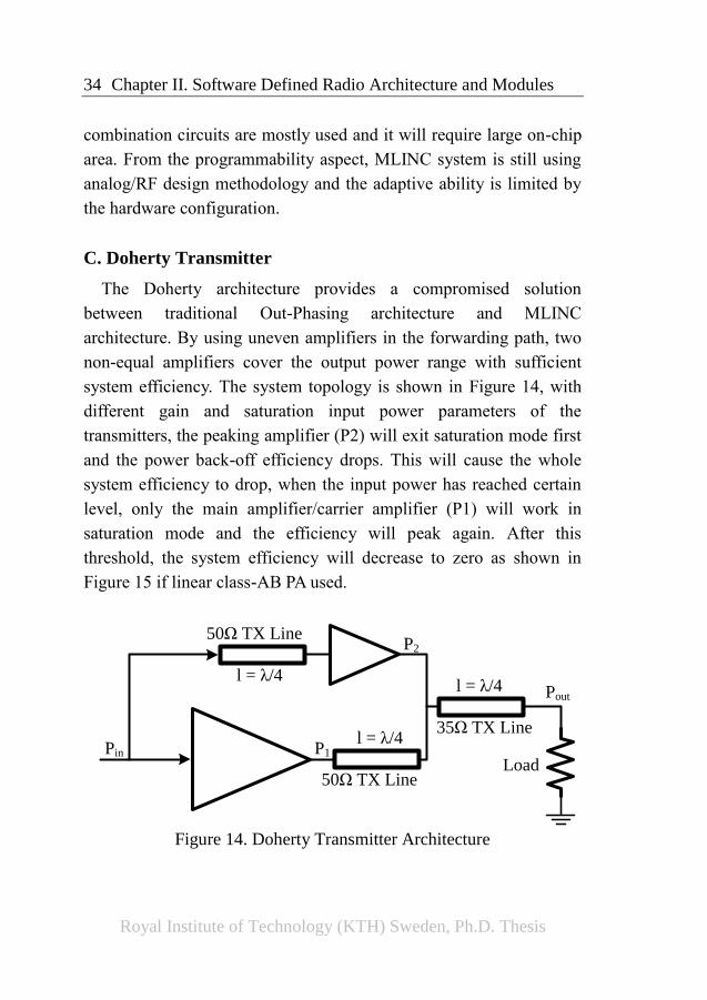
34 Chapter II. Software Defined Radio Architecture and Modules
Royal Institute of Technology (KTH) Sweden, Ph.D. Thesis
combination circuits are mostly used and it will require large on-chip
area. From the programmability aspect, MLINC system is still using
analog/RF design methodology and the adaptive ability is limited by
the hardware configuration.
C. Doherty Transmitter
The Doherty architecture provides a compromised solution
between traditional Out-Phasing architecture and MLINC
architecture. By using uneven amplifiers in the forwarding path, two
non-equal amplifiers cover the output power range with sufficient
system efficiency. The system topology is shown in Figure 14, with
different gain and saturation input power parameters of the
transmitters, the peaking amplifier (P2) will exit saturation mode first
and the power back-off efficiency drops. This will cause the whole
system efficiency to drop, when the input power has reached certain
level, only the main amplifier/carrier amplifier (P1) will work in
saturation mode and the efficiency will peak again. After this
threshold, the system efficiency will decrease to zero as shown in
Figure 15 if linear class-AB PA used.
Pin P1
P2
Pout
Load
35Ω TX Line
50Ω TX Line
50Ω TX Line
l = λ/4
l = λ/4
l = λ/4
Figure 14. Doherty Transmitter Architecture
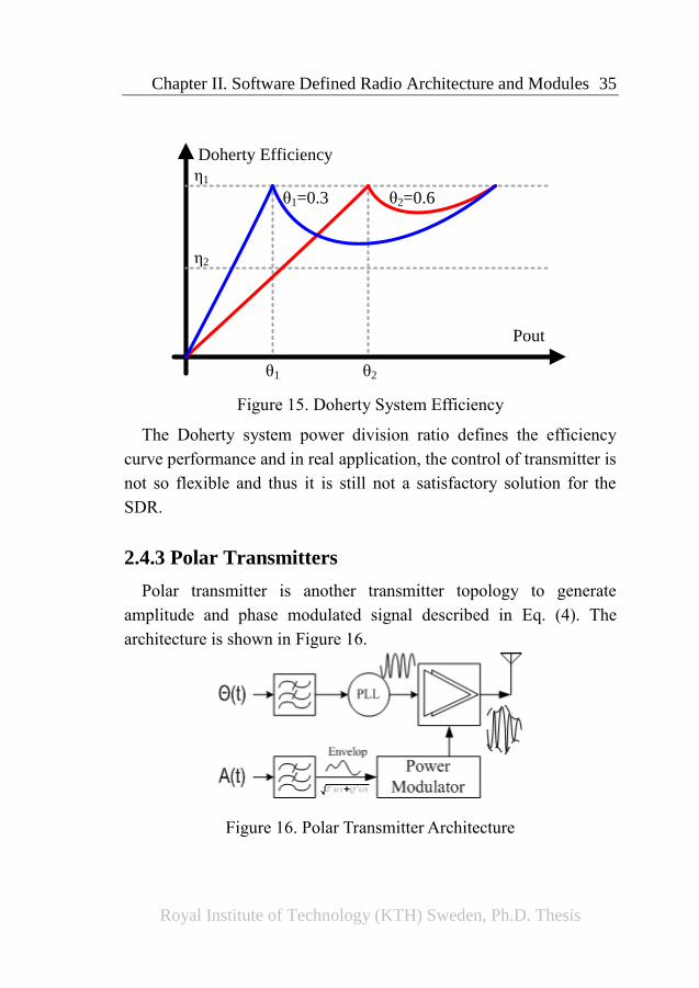
Chapter II. Software Defined Radio Architecture and Modules 35
Royal Institute of Technology (KTH) Sweden, Ph.D. Thesis
Doherty Efficiency
Pout
η1
η2
θ1 θ2
θ1=0.3 θ2=0.6
Figure 15. Doherty System Efficiency
The Doherty system power division ratio defines the efficiency
curve performance and in real application, the control of transmitter is
not so flexible and thus it is still not a satisfactory solution for the
SDR.
2.4.3 Polar Transmitters
Polar transmitter is another transmitter topology to generate
amplitude and phase modulated signal described in Eq. (4). The
architecture is shown in Figure 16.
Figure 16. Polar Transmitter Architecture
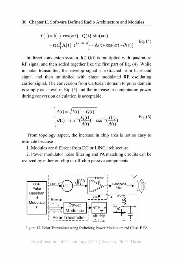
36 Chapter II. Software Defined Radio Architecture and Modules
Royal Institute of Technology (KTH) Sweden, Ph.D. Thesis
j t θ t
t I t cos Q t sin
real A t e A t cos
f t t
t t
Eq. (4)
In direct conversion system, I(t) Q(t) is multiplied with quadrature
RF signal and then added together like the first part of Eq. (4). While
in polar transmitter, the envelop signal is extracted from baseband
signal and then multiplied with phase modulated RF oscillating
carrier signal. The conversion from Cartesian domain to polar domain
is simply as shown in Eq. (5) and the increase in computation power
during conversion calculation is acceptable.
))(
)((cos)
)(
)((sin)(
)()()(
11
22
tA
tI
tA
tQt
tQtItA
Eq. (5)
From topology aspect, the increase in chip area is not so easy to
estimate because
1. Modules are different from DC or LINC architecture.
2. Power modulator noise filtering and PA matching circuits can be
realized by either on-chip or off-chip passive components.
Polar Transmitter
DPLL
Power
Modulator
Class
E
Envelop
Polar
Baseban
d
Modulato
r
DSP
)()( 22 tQtI
),( f
off-chip
LC filter
Bandpass
Filter
Vcc Vcc
Cgd
Figure 17. Polar Transmitter using Switching Power Modulator and Class-E PA
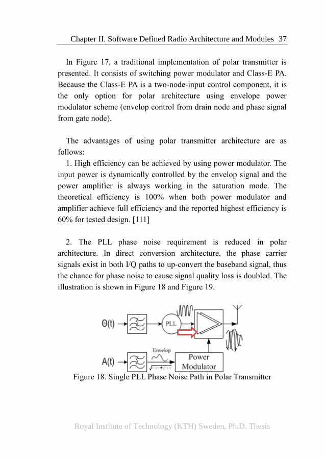
Chapter II. Software Defined Radio Architecture and Modules 37
Royal Institute of Technology (KTH) Sweden, Ph.D. Thesis
In Figure 17, a traditional implementation of polar transmitter is
presented. It consists of switching power modulator and Class-E PA.
Because the Class-E PA is a two-node-input control component, it is
the only option for polar architecture using envelope power
modulator scheme (envelop control from drain node and phase signal
from gate node).
The advantages of using polar transmitter architecture are as
follows:
1. High efficiency can be achieved by using power modulator. The
input power is dynamically controlled by the envelop signal and the
power amplifier is always working in the saturation mode. The
theoretical efficiency is 100% when both power modulator and
amplifier achieve full efficiency and the reported highest efficiency is
60% for tested design. [111]
2. The PLL phase noise requirement is reduced in polar
architecture. In direct conversion architecture, the phase carrier
signals exist in both I/Q paths to up-convert the baseband signal, thus
the chance for phase noise to cause signal quality loss is doubled. The
illustration is shown in Figure 18 and Figure 19.
Figure 18. Single PLL Phase Noise Path in Polar Transmitter
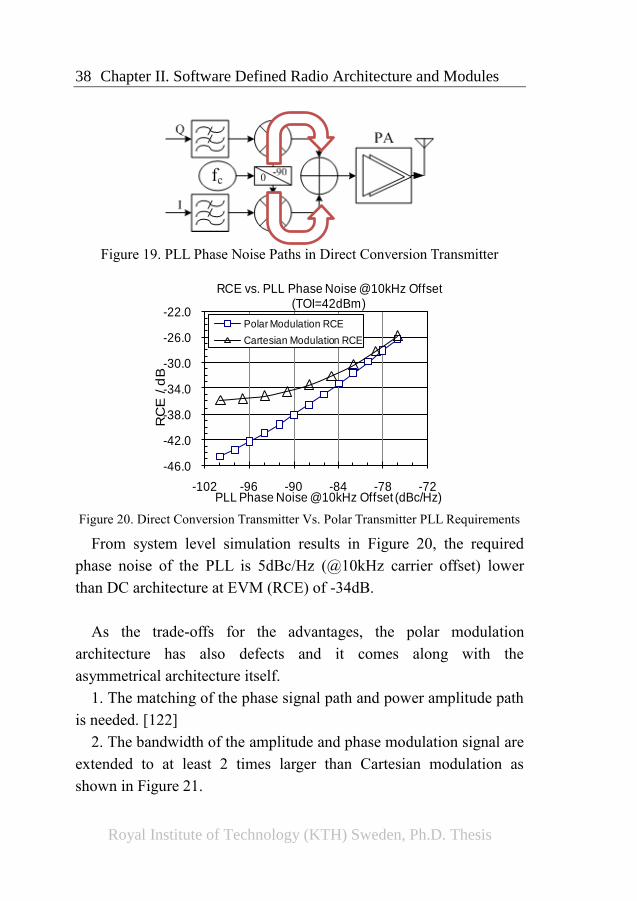
38 Chapter II. Software Defined Radio Architecture and Modules
Royal Institute of Technology (KTH) Sweden, Ph.D. Thesis
Figure 19. PLL Phase Noise Paths in Direct Conversion Transmitter
Figure 20. Direct Conversion Transmitter Vs. Polar Transmitter PLL Requirements
From system level simulation results in Figure 20, the required
phase noise of the PLL is 5dBc/Hz (@10kHz carrier offset) lower
than DC architecture at EVM (RCE) of -34dB.
As the trade-offs for the advantages, the polar modulation
architecture has also defects and it comes along with the
asymmetrical architecture itself.
1. The matching of the phase signal path and power amplitude path
is needed. [122]
2. The bandwidth of the amplitude and phase modulation signal are
extended to at least 2 times larger than Cartesian modulation as
shown in Figure 21.
-46.0
-42.0
-38.0
-34.0
-30.0
-26.0
-22.0
-102 -96 -90 -84 -78 -72
RC
E /
dB
PLL Phase Noise @10kHz Offset (dBc/Hz)
RCE vs. PLL Phase Noise @10kHz Offset (TOI=42dBm)
Polar Modulation RCE
Cartesian Modulation RCE
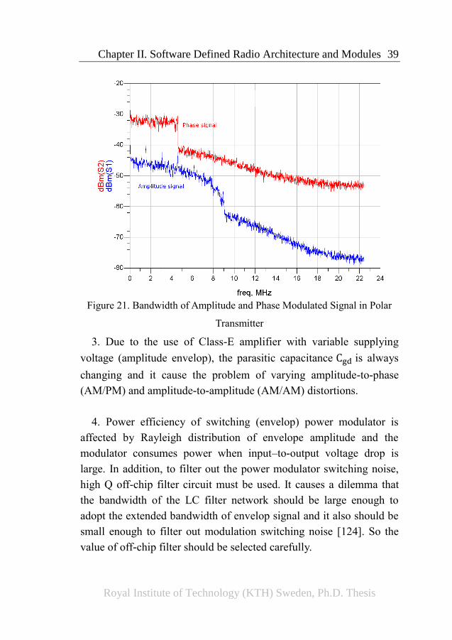
Chapter II. Software Defined Radio Architecture and Modules 39
Royal Institute of Technology (KTH) Sweden, Ph.D. Thesis
Figure 21. Bandwidth of Amplitude and Phase Modulated Signal in Polar
Transmitter
3. Due to the use of Class-E amplifier with variable supplying
voltage (amplitude envelop), the parasitic capacitance Cgd is always
changing and it cause the problem of varying amplitude-to-phase
(AM/PM) and amplitude-to-amplitude (AM/AM) distortions.
4. Power efficiency of switching (envelop) power modulator is
affected by Rayleigh distribution of envelope amplitude and the
modulator consumes power when input–to-output voltage drop is
large. In addition, to filter out the power modulator switching noise,
high Q off-chip filter circuit must be used. It causes a dilemma that
the bandwidth of the LC filter network should be large enough to
adopt the extended bandwidth of envelop signal and it also should be
small enough to filter out modulation switching noise [124]. So the
value of off-chip filter should be selected carefully.
40 Chapter II. Software Defined Radio Architecture and Modules
Royal Institute of Technology (KTH) Sweden, Ph.D. Thesis
In short conclusion on the traditional polar transmitter using Class-
E PA, power combination algorithm is used based on the architecture.
Improvements can be made for polar modulation by taking the
advantage of digital processing to compensate the AM-AM or AM-
PM distortions but for traditional architecture, the effect is limited
due to CMOS transistor feature in low drain voltage situation.
2.4.4 Conclusions on Transmitter Architecture for SDR
The design of SDR transmitter is a process of mapping the
mathematical expression of the transmitted signal into corresponding
transmitter blocks. Among all the transmitter architectures described
above, only the polar transmitter architecture is not involving any
‘accumulation’ operation in the expression, which means there will
not be any analog incremental ‘add’ operation exists in the system. In
polar transmitter, the envelope signal is multiplied with the phase
signal to create the output signal as shown in Eq. (4). From another
point of view, the multiple operations can be easily realized by logic
‘AND’ operation and this implies a possible digital realization. This
feature is complying with the SDR concept and worth further
investigation in real implementation. And based on this thought, the
all-digital polar transmitter will be implemented.
The conclusion for the first question is also answered from the
system level investigation. Polar transmitter architecture is suitable
for the future SDR transceiver solution and it is further explored in
the following work.
Royal Institute of Technology (KTH) Sweden, Ph.D. Thesis
Chapter III. All Digital Polar
Transmitter Design
It is a common concept that switching amplifier is inferior for
systems with high linearity requirements. But based on the evolving
CMOS process and new transmitter architecture, this concept may be
changed in the future. The Nano-CMOS technology is the bricks
build up modern complex systems and it brings the advantages in
many aspects:
A. Manually or automatically dynamic system control. System
modules like gain control, dynamic architecture adjusting, power
management, minimal pin-number real time control interface can be
realized by digital standard cells with minimal on-chip area.
B. Functionality enhancement and digital compensation. Digital
optimization algorithms like searching table or error cancellation is
generally realized in digital format, with advanced digital processing,
more complex algorithms can be integrated in the system to overcome
or fix the non-linearity.
C. Lower power consumption and higher unit gain frequency. The
switching power loss is decreasing with fast switching rise/fall time.
The MOS transistors are acting more digital with process scaling.
For polar amplifier using Class-E PA as last stage, RF power signal
generation is realized in two steps, first the switching modulator
convert DC power into envelop power (power modulation) and then
in the second step, it is combined with phase modulated signal
(frequency up-conversion by Class-E PA). The RF signal generation
is proceed in two places so the power loss still happens when the
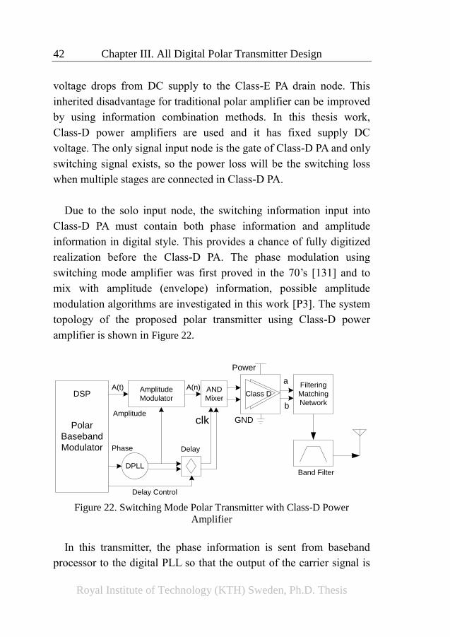
42 Chapter III. All Digital Polar Transmitter Design
Royal Institute of Technology (KTH) Sweden, Ph.D. Thesis
voltage drops from DC supply to the Class-E PA drain node. This
inherited disadvantage for traditional polar amplifier can be improved
by using information combination methods. In this thesis work,
Class-D power amplifiers are used and it has fixed supply DC
voltage. The only signal input node is the gate of Class-D PA and only
switching signal exists, so the power loss will be the switching loss
when multiple stages are connected in Class-D PA.
Due to the solo input node, the switching information input into
Class-D PA must contain both phase information and amplitude
information in digital style. This provides a chance of fully digitized
realization before the Class-D PA. The phase modulation using
switching mode amplifier was first proved in the 70’s [131] and to
mix with amplitude (envelope) information, possible amplitude
modulation algorithms are investigated in this work [P3]. The system
topology of the proposed polar transmitter using Class-D power
amplifier is shown in Figure 22.
Polar
Baseband
Modulator
DSP
DPLL
Amplitude
Amplitude
Modulator
Power
GND
AND
MixerClass D
Delay Control
Band Filter
Filtering
Matching
Network
A(t)
clk
A(n)
Delay
a
b
Phase
Figure 22. Switching Mode Polar Transmitter with Class-D Power
Amplifier
In this transmitter, the phase information is sent from baseband
processor to the digital PLL so that the output of the carrier signal is
Chapter III. All Digital Polar Transmitter Design 43
Royal Institute of Technology (KTH) Sweden, Ph.D. Thesis
phase modulated. The required loop bandwidth of the digital PLL is
larger than traditional PLL based on the system level simulation and
the output wave form is rectified to square wave in digital style.
The amplitude modulator accepts continuous baseband envelop
signal and modulate it into digital format, since the phase signal is
square wave, the envelop amplitude signal should also be in digital
format so that they can be combined to form phase and amplitude
modulated signal. In the system, the modulator clock signal is
provided by the phase modulated carrier signal clock, in this way, two
signals are synchronized. Due to the modulation processing delay, a
delay trimming circuit is needed to match two paths’ timing.
A high speed ‘AND’ standard cell is used as mixer to combine
phase and amplitude digital signal, in this way, phase and amplitude
information is embedded into one and it can drive Class-D PA
directly. The output from Class-D PA is square wave and it needs
‘Filter and Matching’ circuit to restore the phase and amplitude
modulated RF waveforms. Since this part of circuit is consists of
inductive and capacitive components, the switching energy is
accumulated and there is resonation between the primary stage and
secondary stage. Even when there is no switching activity, the
resonating process will sustain the output signal for short period, and
the modulated square wave is converted back to phase and amplitude
modulated RF signal with requested output power (amplitude).
The ‘Filter and Matching’ network is designed to have suitable 3dB
bandwidth. With this feature, the high order harmonics and neighbor
channel noises generated by square wave will be attenuated and the
carrier frequency channel signal is kept. However, the system may
need an extra band filter in case of high quantization noise.
44 Chapter III. All Digital Polar Transmitter Design
Royal Institute of Technology (KTH) Sweden, Ph.D. Thesis
In the next chapter, the detailed analysis on the digital polar
transmitter will be presented and mathematical model analysis will be
given. Except for the digital PLL part, other transmitter blocks are
designed in work [P6].
3.1 All-Digital Polar Transmitter
To verify the digital polar transmitter architecture, the use of
mathematical expression is the first step and then system level models
are built and simulated to identify possible problems that will happen
during the circuit design. As the resolution of system level simulation
is not comparable to circuit level simulation, the results of simulation
may be further improved under next level verification process.
3.1.1 Amplitude Modulation Scheme Selection
The conversion from analog envelop signal to switching signal
format can be realized by different modulation schemes, the mostly
used are Pulse Width Modulation (PWM), Bandpass Delta Sigma
Modulation (BPDSM) and Lowpass Sigma Delta Modulation
(LPSDM) [131]~[140].
In the proposed architecture, upholding system efficiency by using
switching Class-D power amplifier is the most important advantage
and the idea of ‘soft switching’ is part of the key mechanism in this
circuit. The ‘soft switching’ idea is that the switching activity always
happens when the current applied at the switches is minimal or zero,
so that the transistor transition loss is minimized. The spectrum
composition of modulated envelope signal is also revealing the power
distribution, in this case, the more power concentrated in the carrier
Chapter III. All Digital Polar Transmitter Design 45
Royal Institute of Technology (KTH) Sweden, Ph.D. Thesis
frequency, the higher efficiency the system will have.
A. Pulse Width Modulation (PWM)
In PWM modulation, the envelop signal is compared with either a
reference signal which is phase synchronized with the carrier signal
or use the phase modulated carrier signal directly (RF-PWM). In
order to reduce the harmonics level, triangle or sine wave will be used
as comparison reference and the output waveform is shown in Figure
23. Based on the waveform plot, it is theoretically not feasible to
achieve ‘soft switching’.
For the first sight, the output square waveform from PWM
modulation will have varying pulse width related with the input
envelop amplitude and it is usually aligned with the center of
reference signal, so when combined with the phase modulated carrier
signal, the phase information may be distorted at the edge of PWM
modulated output switching signals.
ReferenceInput Output
Figure 23. Pulse Width Modulation Illustration
46 Chapter III. All Digital Polar Transmitter Design
Royal Institute of Technology (KTH) Sweden, Ph.D. Thesis
fc fc+fm fc+2fmfc-fmfc-2fm Figure 24. PWM Up-converted Spectrum
In the second place, when phase modulated carrier is used as
reference directly, switching loss happens every carrier cycle as
illustrated in Figure 26. When small envelop is processed, due to the
fast reference signal, narrow pulses may not be generated by the
comparator so ‘bits loss’ may happen.
From spectrum aspect, after PWM modulation, the up-converted
output signal will have spectrum as shown in Figure 24. In which fm
is the PWM modulation frequency and fc is the carrier frequency.
When RF-PWM is used, modulation harmonics will disappear in the
notch of PWM square window spectrum response.
Since the sum of all the spectrum power come from the drain
supply node in class-D amplifier, the power contained in the
modulation harmonics is taken considerable portion in the whole
input drain power. From system aspect, RF-PWM will have lower
band filter design challenge but higher comparator design challenges.
The switching loss in both RF-PWM and low-frequency-reference
PWM are almost the same and ‘soft switching’ is not possible.
B. Bandpass Delta Sigma Modulation (BPDSM)
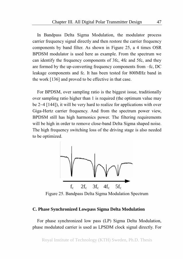
Chapter III. All Digital Polar Transmitter Design 47
Royal Institute of Technology (KTH) Sweden, Ph.D. Thesis
In Bandpass Delta Sigma Modulation, the modulator process
carrier frequency signal directly and then restore the carrier frequency
components by band filter. As shown in Figure 25, a 4 times OSR
BPDSM modulator is used here as example. From the spectrum we
can identify the frequency components of 3fc, 4fc and 5fc, and they
are formed by the up-converting frequency components from –fc, DC
leakage components and fc. It has been tested for 800MHz band in
the work [136] and proved to be effective in that case.
For BPDSM, over sampling ratio is the biggest issue, traditionally
over sampling ratio higher than 1 is required (the optimum value may
be 2~4 [144]), it will be very hard to realize for applications with over
Giga-Hertz carrier frequency. And from the spectrum power view,
BPDSM still has high harmonics power. The filtering requirements
will be high in order to remove close-band Delta Sigma shaped noise.
The high frequency switching loss of the driving stage is also needed
to be optimized.
fc 3fc 5fc2fc 4fc Figure 25. Bandpass Delta Sigma Modulation Spectrum
C. Phase Synchronized Lowpass Sigma Delta Modulation
For phase synchronized low pass (LP) Sigma Delta Modulation,
phase modulated carrier is used as LPSDM clock signal directly. For
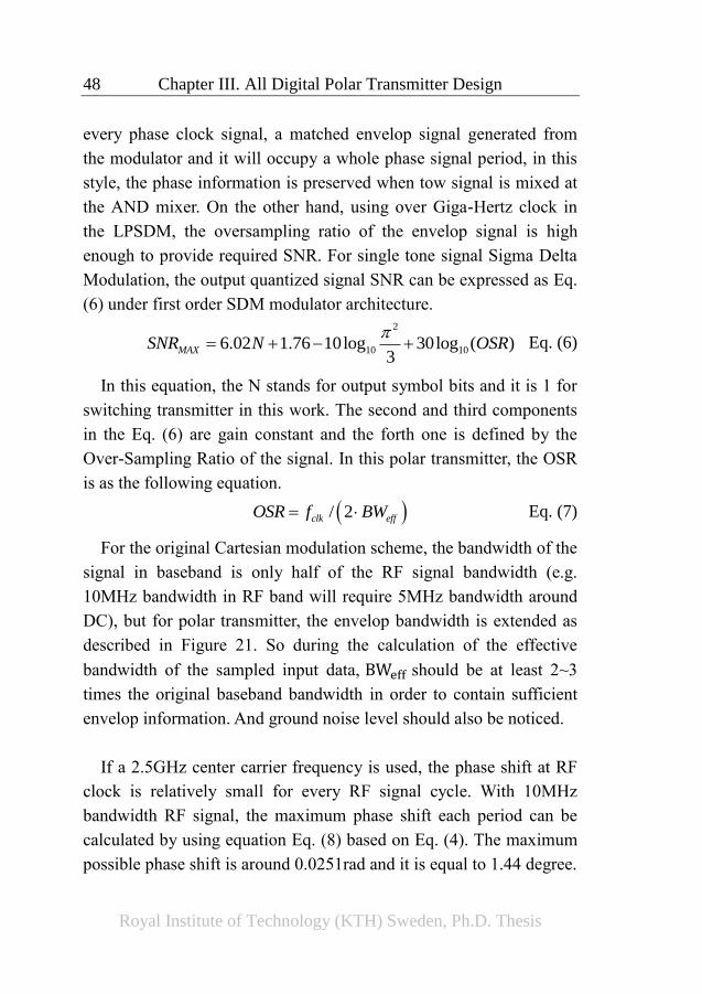
48 Chapter III. All Digital Polar Transmitter Design
Royal Institute of Technology (KTH) Sweden, Ph.D. Thesis
every phase clock signal, a matched envelop signal generated from
the modulator and it will occupy a whole phase signal period, in this
style, the phase information is preserved when tow signal is mixed at
the AND mixer. On the other hand, using over Giga-Hertz clock in
the LPSDM, the oversampling ratio of the envelop signal is high
enough to provide required SNR. For single tone signal Sigma Delta
Modulation, the output quantized signal SNR can be expressed as Eq.
(6) under first order SDM modulator architecture.
2
10 106.02 1.76 10log 30log ( )3
MAXSNR N OSR
Eq. (6)
In this equation, the N stands for output symbol bits and it is 1 for
switching transmitter in this work. The second and third components
in the Eq. (6) are gain constant and the forth one is defined by the
Over-Sampling Ratio of the signal. In this polar transmitter, the OSR
is as the following equation.
/ 2clk effOSR f BW Eq. (7)
For the original Cartesian modulation scheme, the bandwidth of the
signal in baseband is only half of the RF signal bandwidth (e.g.
10MHz bandwidth in RF band will require 5MHz bandwidth around
DC), but for polar transmitter, the envelop bandwidth is extended as
described in Figure 21. So during the calculation of the effective
bandwidth of the sampled input data, BWeff should be at least 2~3
times the original baseband bandwidth in order to contain sufficient
envelop information. And ground noise level should also be noticed.
If a 2.5GHz center carrier frequency is used, the phase shift at RF
clock is relatively small for every RF signal cycle. With 10MHz
bandwidth RF signal, the maximum phase shift each period can be
calculated by using equation Eq. (8) based on Eq. (4). The maximum
possible phase shift is around 0.0251rad and it is equal to 1.44 degree.
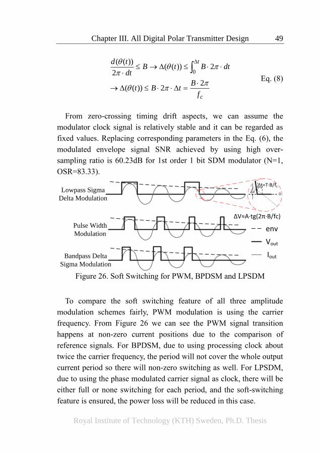
Chapter III. All Digital Polar Transmitter Design 49
Royal Institute of Technology (KTH) Sweden, Ph.D. Thesis
c
t
f
BtBt
dtBtBdt
td
22))((
2))((2
))((
0
Eq. (8)
From zero-crossing timing drift aspects, we can assume the
modulator clock signal is relatively stable and it can be regarded as
fixed values. Replacing corresponding parameters in the Eq. (6), the
modulated envelope signal SNR achieved by using high over-
sampling ratio is 60.23dB for 1st order 1 bit SDM modulator (N=1,
OSR=83.33).
0
Δt=T·B/fc
ΔV≈A·tg(2π·B/fc)
ΔVLowpass Sigma
Delta Modulation
env
Iout
Vout
Pulse Width
Modulation
Bandpass Delta
Sigma Modulation
Figure 26. Soft Switching for PWM, BPDSM and LPSDM
To compare the soft switching feature of all three amplitude
modulation schemes fairly, PWM modulation is using the carrier
frequency. From Figure 26 we can see the PWM signal transition
happens at non-zero current positions due to the comparison of
reference signals. For BPDSM, due to using processing clock about
twice the carrier frequency, the period will not cover the whole output
current period so there will non-zero switching as well. For LPSDM,
due to using the phase modulated carrier signal as clock, there will be
either full or none switching for each period, and the soft-switching
feature is ensured, the power loss will be reduced in this case.
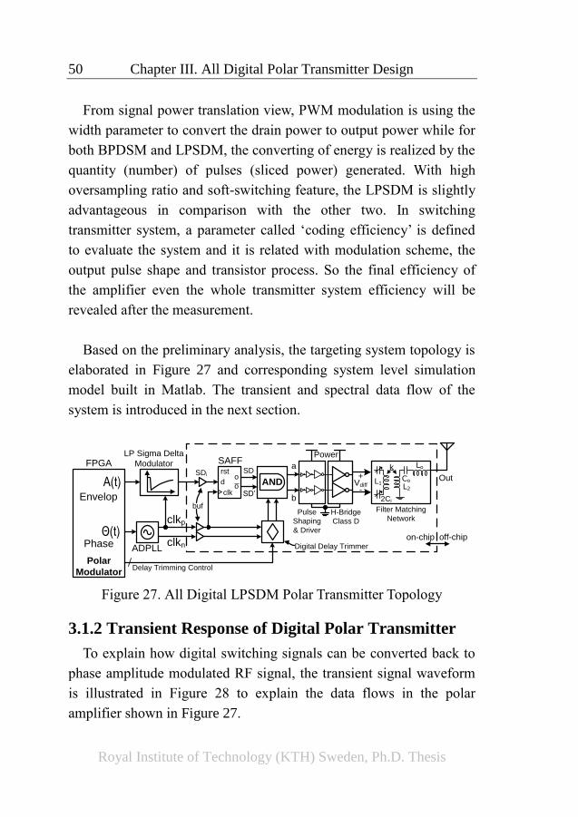
50 Chapter III. All Digital Polar Transmitter Design
Royal Institute of Technology (KTH) Sweden, Ph.D. Thesis
From signal power translation view, PWM modulation is using the
width parameter to convert the drain power to output power while for
both BPDSM and LPSDM, the converting of energy is realized by the
quantity (number) of pulses (sliced power) generated. With high
oversampling ratio and soft-switching feature, the LPSDM is slightly
advantageous in comparison with the other two. In switching
transmitter system, a parameter called ‘coding efficiency’ is defined
to evaluate the system and it is related with modulation scheme, the
output pulse shape and transistor process. So the final efficiency of
the amplifier even the whole transmitter system efficiency will be
revealed after the measurement.
Based on the preliminary analysis, the targeting system topology is
elaborated in Figure 27 and corresponding system level simulation
model built in Matlab. The transient and spectral data flow of the
system is introduced in the next section.
FPGA
Envelop
Power
H-Bridge
Class D
Delay Trimming Control
A(t)SD
a
b
Θ(t)
ADPLL
OutAND
LP Sigma Delta
Modulator
Polar
Modulator
clkp
off-chipon-chip
Pulse
Shaping
& Driver
clkn
Filter Matching
Network
k
L1
2Ci
L2SD’
Lo
Co
Phase
SDi
SAFF
clk
d
buf
o
o
+Vdiff
-
rst
Digital Delay Trimmer
Figure 27. All Digital LPSDM Polar Transmitter Topology
3.1.2 Transient Response of Digital Polar Transmitter
To explain how digital switching signals can be converted back to
phase amplitude modulated RF signal, the transient signal waveform
is illustrated in Figure 28 to explain the data flows in the polar
amplifier shown in Figure 27.
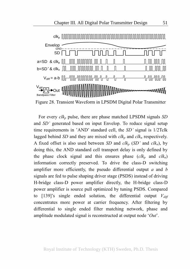
Chapter III. All Digital Polar Transmitter Design 51
Royal Institute of Technology (KTH) Sweden, Ph.D. Thesis
a=SD & clkp
clkp
SD
Vdiff = a-b
Out
Envelop
b=SD’& clkn
Bandpass Filter
Vdiff
GND
Figure 28. Transient Waveform in LPSDM Digital Polar Transmitter
For every clkp pulse, there are phase matched LPSDM signals SD
and SD’ generated based on input Envelop. To reduce signal setup
time requirements in ’AND’ standard cell, the SD’ signal is 1/2Tclk
lagged behind SD and they are mixed with clkp and clkn respectively.
A fixed offset is also used between SD and clkp (SD’ and clkn), by
doing this, the AND standard cell transport delay is only defined by
the phase clock signal and this ensures phase (clkp and clkn)
information correctly preserved. To drive the class-D switching
amplifier more efficiently, the pseudo differential output a and b
signals are fed to pulse shaping driver stage (PSDS) instead of driving
H-bridge class-D power amplifier directly, the H-bridge class-D
power amplifier is source pull optimized by tuning PSDS. Compared
to [139]’s single ended solution, the differential output Vdiff
concentrates more power at carrier frequency. After filtering by
differential to single ended filter matching network, phase and
amplitude modulated signal is reconstructed at output node ‘Out’.
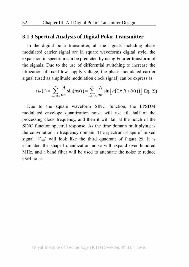
52 Chapter III. All Digital Polar Transmitter Design
Royal Institute of Technology (KTH) Sweden, Ph.D. Thesis
3.1.3 Spectral Analysis of Digital Polar Transmitter
In the digital polar transmitter, all the signals including phase
modulated carrier signal are in square waveforms digital style, the
expansion in spectrum can be predicted by using Fourier transform of
the signals. Due to the use of differential switching to increase the
utilization of fixed low supply voltage, the phase modulated carrier
signal (used as amplitude modulation clock signal) can be express as
1,3,5 1,3,5
( ) sin( ) sin 2 ( )n n
A Aclk t n t n ft t
n n
Eq. (9)
Due to the square waveform SINC function, the LPSDM
modulated envelope quantization noise will rise till half of the
processing clock frequency, and then it will fall at the notch of the
SINC function spectral response. As the time domain multiplying is
the convolution in frequency domain. The spectrum shape of mixed
signal ‘Vdiff’ will look like the third quadrant of Figure 29. It is
estimated the shaped quantization noise will expand over hundred
MHz, and a band filter will be used to attenuate the noise to reduce
OoB noise.
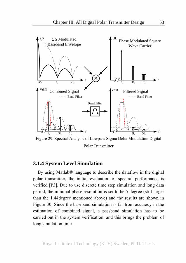
Chapter III. All Digital Polar Transmitter Design 53
Royal Institute of Technology (KTH) Sweden, Ph.D. Thesis
f
SD ΣΔ Modulated
Baseband Envelope
f
clk
fc 3fc 5fc
Phase Modulated Square
Wave Carrier
Vdiff
fc 3fc 5fc
Combined Signal
Band Filter
B/2
Band Filter
Vout Filtered Signal
Band Filter
fc 2fc
3fc 5fcf f
Figure 29. Spectral Analysis of Lowpass Sigma Delta Modulation Digital
Polar Transmitter
3.1.4 System Level Simulation
By using Matlab® language to describe the dataflow in the digital
polar transmitter, the initial evaluation of spectral performance is
verified [P3]. Due to use discrete time step simulation and long data
period, the minimal phase resolution is set to be 5 degree (still larger
than the 1.44degree mentioned above) and the results are shown in
Figure 30. Since the baseband simulation is far from accuracy in the
estimation of combined signal, a passband simulation has to be
carried out in the system verification, and this brings the problem of
long simulation time.
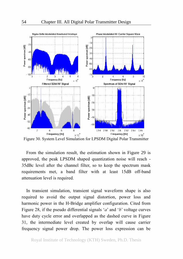
54 Chapter III. All Digital Polar Transmitter Design
Royal Institute of Technology (KTH) Sweden, Ph.D. Thesis
Figure 30. System Level Simulation for LPSDM Digital Polar Transmitter
From the simulation result, the estimation shown in Figure 29 is
approved, the peak LPSDM shaped quantization noise will reach -
35dBc level after the channel filter, so to keep the spectrum mask
requirements met, a band filter with at least 15dB off-band
attenuation level is required.
In transient simulation, transient signal waveform shape is also
required to avoid the output signal distortion, power loss and
harmonic power in the H-Bridge amplifier configuration. Cited from
Figure 28, if the pseudo differential signals ‘a’ and ‘b’ voltage curves
have duty cycle error and overlapped as the dashed curve in Figure
31, the intermediate level created by overlap will cause carrier
frequency signal power drop. The power loss expression can be
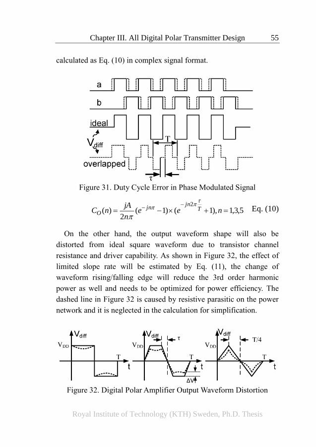
Chapter III. All Digital Polar Transmitter Design 55
Royal Institute of Technology (KTH) Sweden, Ph.D. Thesis
calculated as Eq. (10) in complex signal format.
Figure 31. Duty Cycle Error in Phase Modulated Signal
5,3,1),1()1(2
)(2
neen
jAnC T
jnjn
O
Eq. (10)
On the other hand, the output waveform shape will also be
distorted from ideal square waveform due to transistor channel
resistance and driver capability. As shown in Figure 32, the effect of
limited slope rate will be estimated by Eq. (11), the change of
waveform rising/falling edge will reduce the 3rd order harmonic
power as well and needs to be optimized for power efficiency. The
dashed line in Figure 32 is caused by resistive parasitic on the power
network and it is neglected in the calculation for simplification.
Figure 32. Digital Polar Amplifier Output Waveform Distortion
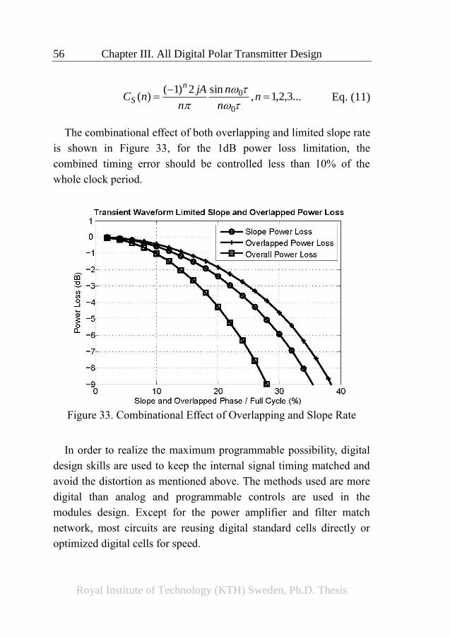
56 Chapter III. All Digital Polar Transmitter Design
Royal Institute of Technology (KTH) Sweden, Ph.D. Thesis
...3,2,1,sin2)1(
)(0
0
nn
n
n
jAnC
n
S
Eq. (11)
The combinational effect of both overlapping and limited slope rate
is shown in Figure 33, for the 1dB power loss limitation, the
combined timing error should be controlled less than 10% of the
whole clock period.
Figure 33. Combinational Effect of Overlapping and Slope Rate
In order to realize the maximum programmable possibility, digital
design skills are used to keep the internal signal timing matched and
avoid the distortion as mentioned above. The methods used are more
digital than analog and programmable controls are used in the
modules design. Except for the power amplifier and filter match
network, most circuits are reusing digital standard cells directly or
optimized digital cells for speed.
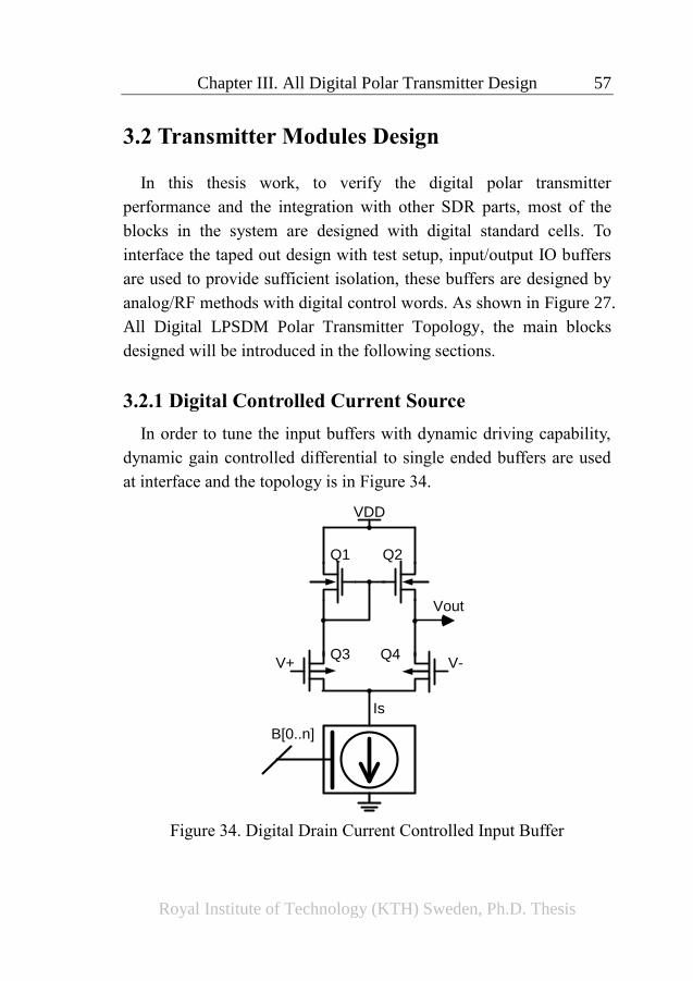
Chapter III. All Digital Polar Transmitter Design 57
Royal Institute of Technology (KTH) Sweden, Ph.D. Thesis
3.2 Transmitter Modules Design
In this thesis work, to verify the digital polar transmitter
performance and the integration with other SDR parts, most of the
blocks in the system are designed with digital standard cells. To
interface the taped out design with test setup, input/output IO buffers
are used to provide sufficient isolation, these buffers are designed by
analog/RF methods with digital control words. As shown in Figure 27.
All Digital LPSDM Polar Transmitter Topology, the main blocks
designed will be introduced in the following sections.
3.2.1 Digital Controlled Current Source
In order to tune the input buffers with dynamic driving capability,
dynamic gain controlled differential to single ended buffers are used
at interface and the topology is in Figure 34.
``
VDD
V+ V-
Vout
B[0..n]
Q1 Q2
Q3 Q4
Is
Figure 34. Digital Drain Current Controlled Input Buffer
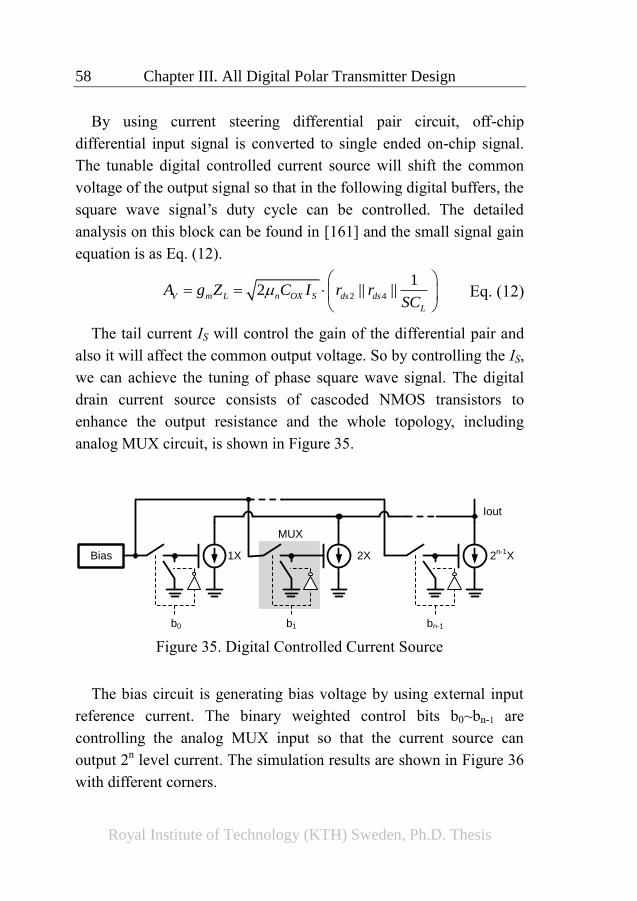
58 Chapter III. All Digital Polar Transmitter Design
Royal Institute of Technology (KTH) Sweden, Ph.D. Thesis
By using current steering differential pair circuit, off-chip
differential input signal is converted to single ended on-chip signal.
The tunable digital controlled current source will shift the common
voltage of the output signal so that in the following digital buffers, the
square wave signal’s duty cycle can be controlled. The detailed
analysis on this block can be found in [161] and the small signal gain
equation is as Eq. (12).
2 4
12 || ||V m L n OX S ds ds
L
A g Z C I r rSC
Eq. (12)
The tail current IS will control the gain of the differential pair and
also it will affect the common output voltage. So by controlling the IS,
we can achieve the tuning of phase square wave signal. The digital
drain current source consists of cascoded NMOS transistors to
enhance the output resistance and the whole topology, including
analog MUX circuit, is shown in Figure 35.
Bias 2X1X 2n-1
X
b0 b1 bn-1
Iout
MUX
Figure 35. Digital Controlled Current Source
The bias circuit is generating bias voltage by using external input
reference current. The binary weighted control bits b0~bn-1 are
controlling the analog MUX input so that the current source can
output 2n level current. The simulation results are shown in Figure 36
with different corners.
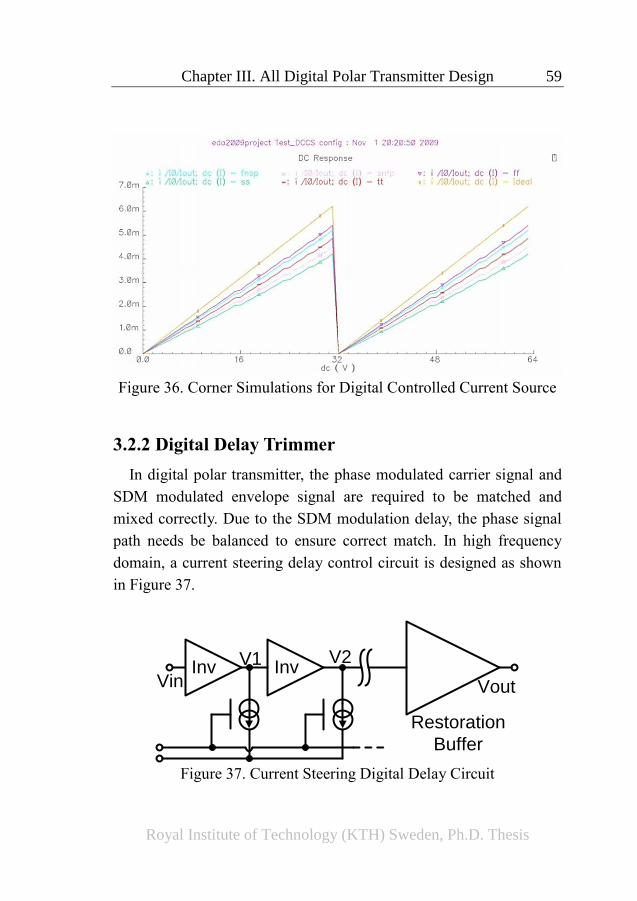
Chapter III. All Digital Polar Transmitter Design 59
Royal Institute of Technology (KTH) Sweden, Ph.D. Thesis
Figure 36. Corner Simulations for Digital Controlled Current Source
3.2.2 Digital Delay Trimmer
In digital polar transmitter, the phase modulated carrier signal and
SDM modulated envelope signal are required to be matched and
mixed correctly. Due to the SDM modulation delay, the phase signal
path needs be balanced to ensure correct match. In high frequency
domain, a current steering delay control circuit is designed as shown
in Figure 37.
Inv Inv
Restoration
Buffer
Vin
V1 V2
Vout
Figure 37. Current Steering Digital Delay Circuit
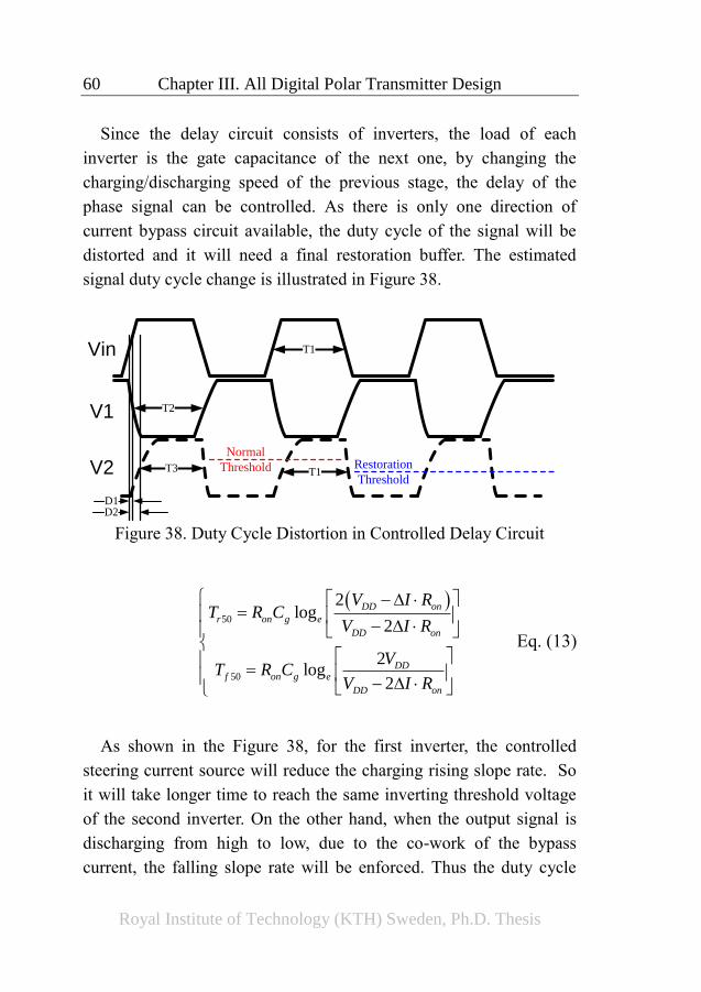
60 Chapter III. All Digital Polar Transmitter Design
Royal Institute of Technology (KTH) Sweden, Ph.D. Thesis
Since the delay circuit consists of inverters, the load of each
inverter is the gate capacitance of the next one, by changing the
charging/discharging speed of the previous stage, the delay of the
phase signal can be controlled. As there is only one direction of
current bypass circuit available, the duty cycle of the signal will be
distorted and it will need a final restoration buffer. The estimated
signal duty cycle change is illustrated in Figure 38.
T1T3
T2
D1D2
Restoration
Threshold
Normal
Threshold
Vin
V1
V2
T1
Figure 38. Duty Cycle Distortion in Controlled Delay Circuit
50
50
2log
2
2log
2
DD on
r on g e
DD on
DDf on g e
DD on
V I RT R C
V I R
VT R C
V I R
Eq. (13)
As shown in the Figure 38, for the first inverter, the controlled
steering current source will reduce the charging rising slope rate. So
it will take longer time to reach the same inverting threshold voltage
of the second inverter. On the other hand, when the output signal is
discharging from high to low, due to the co-work of the bypass
current, the falling slope rate will be enforced. Thus the duty cycle
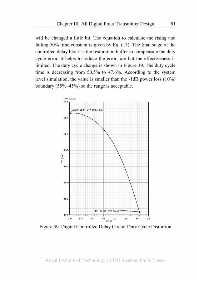
Chapter III. All Digital Polar Transmitter Design 61
Royal Institute of Technology (KTH) Sweden, Ph.D. Thesis
will be changed a little bit. The equation to calculate the rising and
falling 50% time constant is given by Eq. (13). The final stage of the
controlled delay block is the restoration buffer to compensate the duty
cycle error, it helps to reduce the error rate but the effectiveness is
limited. The duty cycle change is shown in Figure 39. The duty cycle
time is decreasing from 50.5% to 47.6%. According to the system
level simulation, the value is smaller than the -1dB power loss (10%)
boundary (55%~45%) so the range is acceptable.
Figure 39. Digital Controlled Delay Circuit Duty Cycle Distortion
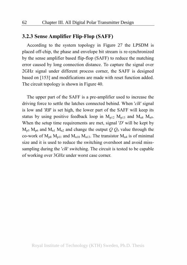
62 Chapter III. All Digital Polar Transmitter Design
Royal Institute of Technology (KTH) Sweden, Ph.D. Thesis
3.2.3 Sense Amplifier Flip-Flop (SAFF)
According to the system topology in Figure 27 the LPSDM is
placed off-chip, the phase and envelope bit stream is re-synchronized
by the sense amplifier based flip-flop (SAFF) to reduce the matching
error caused by long connection distance. To capture the signal over
2GHz signal under different process corner, the SAFF is designed
based on [153] and modifications are made with reset function added.
The circuit topology is shown in Figure 40.
The upper part of the SAFF is a pre-amplifier used to increase the
driving force to settle the latches connected behind. When 'clk' signal
is low and 'RB' is set high, the lower part of the SAFF will keep its
status by using positive feedback loop in Mp12 Mp13 and Mn8 Mn9.
When the setup time requirements are met, signal 'D' will be kept by
Mp5 Mp6 and Mn1 Mn2 and change the output Q Qb value through the
co-work of Mp8 Mp11 and Mn10 Mn13. The transistor Mn4 is of minimal
size and it is used to reduce the switching overshoot and avoid miss-
sampling during the 'clk' switching. The circuit is tested to be capable
of working over 3GHz under worst case corner.
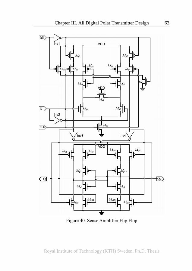
Chapter III. All Digital Polar Transmitter Design 63
Royal Institute of Technology (KTH) Sweden, Ph.D. Thesis
Figure 40. Sense Amplifier Flip Flop
64 Chapter III. All Digital Polar Transmitter Design
Royal Institute of Technology (KTH) Sweden, Ph.D. Thesis
3.2.4 Switching Power Amplifier Optimization
Since the Class-D PA is non-linear, the measurement of peak output
power, gain or linearity like IM3 cannot be realized by traditional
methods, instead of spectral domain small signal simulation, large
signal transient signal simulation has to be used in the design. Then
all the test results should be extracted from transient simulation. The
optimization of CMOS transistor size for certain load and
corresponding output power is also carried out in transient simulation.
To identify the suitable load value and then optimize the PA,
estimation is performed based on the process limitations, the top
metal reserved for the transformer is capable of supporting 8mA per
micrometer and 10um metal width is chosen for the transformer. The
average peak current supported is 80mA and transient peak is 4/pi
times larger, so the peak current is 101.86mA. For an equivalent load
at the primary stage of the transformer, it will be 2VDD/IMAX and it is
equal to 20 Ohm in the design. To remove the higher order harmonics
and convert square wave to analog signal, a simple 2nd order LC
filter is used and serial connected with the equivalent load.
The optimization is mainly targeting two parameters, the efficiency
and output power, the efficiency is the primary requirement and the
size of the PN-MOS in Class-D PA is tuned. Since the large Class-D
PA cannot be driven directly, ‘exponential horn’ topology is used and
it consists of size-up inverters as shown in Figure 41. The
corresponding power loss model is also built upon the circuit
topology and the equation is given in Eq. (14).
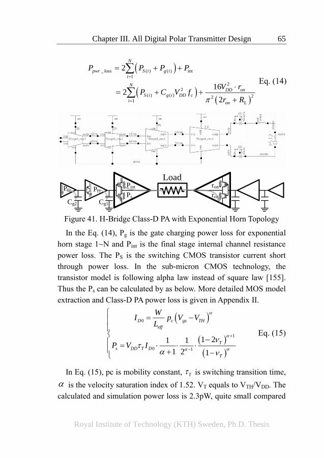
Chapter III. All Digital Polar Transmitter Design 65
Royal Institute of Technology (KTH) Sweden, Ph.D. Thesis
_ ( ) ( ) int
1
2
2
( ) ( ) 221
2
162
2
N
pwr loss S i g i
i
NDD on
S i g i DD c
i on L
P P P P
V rP C V f
r R
Eq. (14)
Ps
Load
Pl1
Cg1
Pint ron
ron
Pl2
Cg2
Figure 41. H-Bridge Class-D PA with Exponential Horn Topology
In the Eq. (14), Pg is the gate charging power loss for exponential
horn stage 1~N and Pint is the final stage internal channel resistance
power loss. The PS is the switching CMOS transistor current short
through power loss. In the sub-micron CMOS technology, the
transistor model is following alpha law instead of square law [155].
Thus the Ps can be calculated by as below. More detailed MOS model
extraction and Class-D PA power loss is given in Appendix II.
0
1
0 1
1 21 1
1 2 1
D c gs TH
eff
T
s DD T D
T
WI p V V
L
P V I
Eq. (15)
In Eq. (15), pc is mobility constant, T is switching transition time,
is the velocity saturation index of 1.52. VT equals to VTH/VDD. The
calculated and simulation power loss is 2.3pW, quite small compared
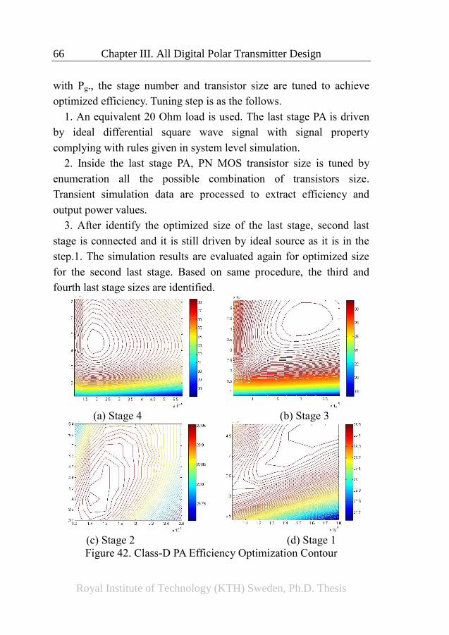
66 Chapter III. All Digital Polar Transmitter Design
Royal Institute of Technology (KTH) Sweden, Ph.D. Thesis
with Pg., the stage number and transistor size are tuned to achieve
optimized efficiency. Tuning step is as the follows.
1. An equivalent 20 Ohm load is used. The last stage PA is driven
by ideal differential square wave signal with signal property
complying with rules given in system level simulation.
2. Inside the last stage PA, PN MOS transistor size is tuned by
enumeration all the possible combination of transistors size.
Transient simulation data are processed to extract efficiency and
output power values.
3. After identify the optimized size of the last stage, second last
stage is connected and it is still driven by ideal source as it is in the
step.1. The simulation results are evaluated again for optimized size
for the second last stage. Based on same procedure, the third and
fourth last stage sizes are identified.
(a) Stage 4 (b) Stage 3
(c) Stage 2 (d) Stage 1
Figure 42. Class-D PA Efficiency Optimization Contour
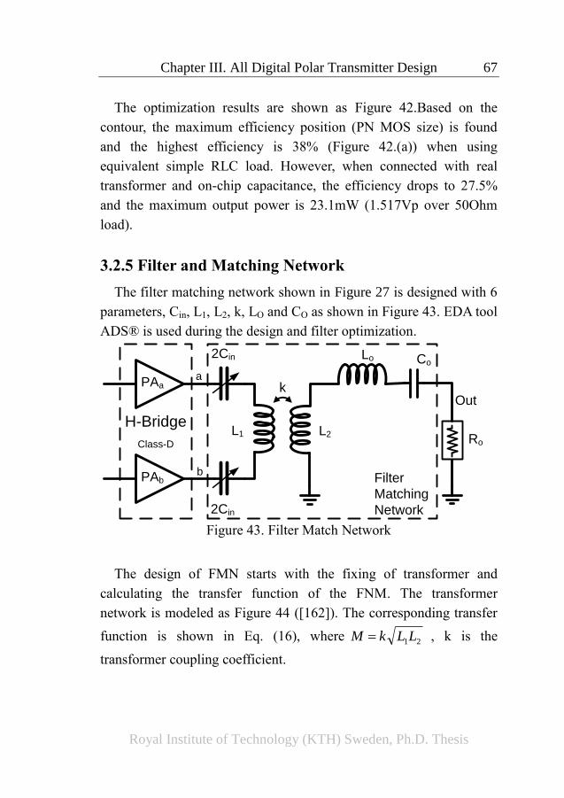
Chapter III. All Digital Polar Transmitter Design 67
Royal Institute of Technology (KTH) Sweden, Ph.D. Thesis
The optimization results are shown as Figure 42.Based on the
contour, the maximum efficiency position (PN MOS size) is found
and the highest efficiency is 38% (Figure 42.(a)) when using
equivalent simple RLC load. However, when connected with real
transformer and on-chip capacitance, the efficiency drops to 27.5%
and the maximum output power is 23.1mW (1.517Vp over 50Ohm
load).
3.2.5 Filter and Matching Network
The filter matching network shown in Figure 27 is designed with 6
parameters, Cin, L1, L2, k, LO and CO as shown in Figure 43. EDA tool
ADS® is used during the design and filter optimization.
k
L2L1
2Cin
2Cin
Lo Co
Ro
H-Bridge
Class-D
PAa
PAb
a
b
Out
Filter
Matching
Network
Figure 43. Filter Match Network
The design of FMN starts with the fixing of transformer and
calculating the transfer function of the FNM. The transformer
network is modeled as Figure 44 ([162]). The corresponding transfer
function is shown in Eq. (16), where , k is the
transformer coupling coefficient.
21LLkM
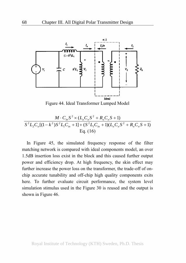
68 Chapter III. All Digital Polar Transmitter Design
Royal Institute of Technology (KTH) Sweden, Ph.D. Thesis
Figure 44. Ideal Transformer Lumped Model
Eq. (16)
In Figure 45, the simulated frequency response of the filter
matching network is compared with ideal components model, an over
1.5dB insertion loss exist in the block and this caused further output
power and efficiency drop. At high frequency, the skin effect may
further increase the power loss on the transformer, the trade-off of on-
chip accurate tunability and off-chip high quality components exits
here. To further evaluate circuit performance, the system level
simulation stimulus used in the Figure 30 is reused and the output is
shown in Figure 46.
)1)(1(]1)1[(
)1(2
1
2
1
22
2
2
22
SCRSCLCLSCLSkCLS
SCRSCLSCM
ooooinino
ooooin
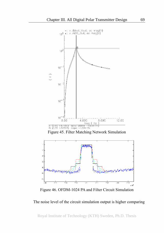
Chapter III. All Digital Polar Transmitter Design 69
Royal Institute of Technology (KTH) Sweden, Ph.D. Thesis
Figure 45. Filter Matching Network Simulation
Figure 46. OFDM-1024 PA and Filter Circuit Simulation
The noise level of the circuit simulation output is higher comparing
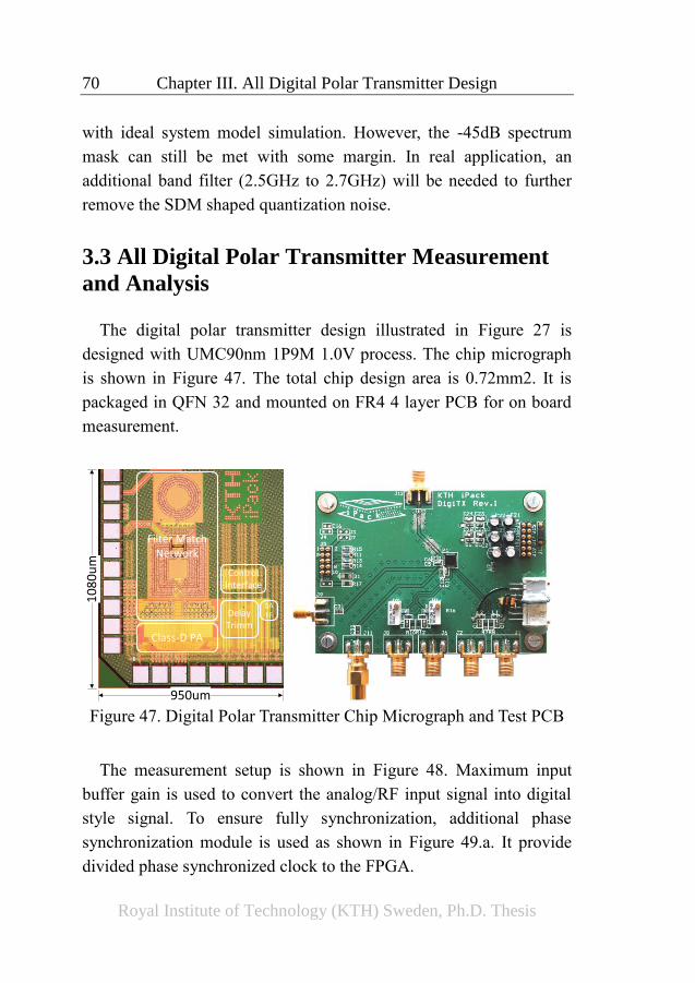
70 Chapter III. All Digital Polar Transmitter Design
Royal Institute of Technology (KTH) Sweden, Ph.D. Thesis
with ideal system model simulation. However, the -45dB spectrum
mask can still be met with some margin. In real application, an
additional band filter (2.5GHz to 2.7GHz) will be needed to further
remove the SDM shaped quantization noise.
3.3 All Digital Polar Transmitter Measurement
and Analysis
The digital polar transmitter design illustrated in Figure 27 is
designed with UMC90nm 1P9M 1.0V process. The chip micrograph
is shown in Figure 47. The total chip design area is 0.72mm2. It is
packaged in QFN 32 and mounted on FR4 4 layer PCB for on board
measurement.
Filter Match Network
Class-D PA
Control Interface
Delay Trimm
SAFF
950um
10
80
um
Figure 47. Digital Polar Transmitter Chip Micrograph and Test PCB
The measurement setup is shown in Figure 48. Maximum input
buffer gain is used to convert the analog/RF input signal into digital
style signal. To ensure fully synchronization, additional phase
synchronization module is used as shown in Figure 49.a. It provide
divided phase synchronized clock to the FPGA.
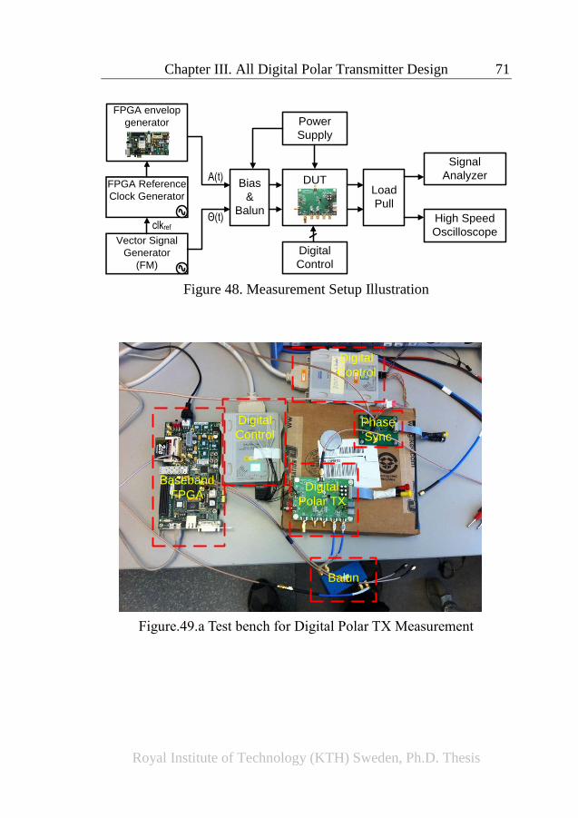
Chapter III. All Digital Polar Transmitter Design 71
Royal Institute of Technology (KTH) Sweden, Ph.D. Thesis
DUT
Vector Signal
Generator
(FM)
Digital
Control
A(t)
Θ(t)
Power
Supply
Signal
Analyzer
High Speed
Oscilloscope
FPGA Reference
Clock Generator
FPGA envelop
generator
clkref
Bias
&
Balun
Load
Pull
Figure 48. Measurement Setup Illustration
Digital
Control
Baseband
FPGA
Digital
Control
Digital
Polar TX
Phase
Sync
Balun
Figure.49.a Test bench for Digital Polar TX Measurement
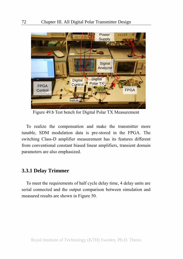
72 Chapter III. All Digital Polar Transmitter Design
Royal Institute of Technology (KTH) Sweden, Ph.D. Thesis
FPGA
Control
Signal
Analyzer
Power
Supply
balun
Digital
Control
FPGA
Digital
Polar TX
Figure 49.b Test bench for Digital Polar TX Measurement
To realize the compensation and make the transmitter more
tunable, SDM modulation data is pre-stored in the FPGA. The
switching Class-D amplifier measurement has its features different
from conventional constant biased linear amplifiers, transient domain
parameters are also emphasized.
3.3.1 Delay Trimmer
To meet the requirements of half cycle delay time, 4 delay units are
serial connected and the output comparison between simulation and
measured results are shown in Figure 50.
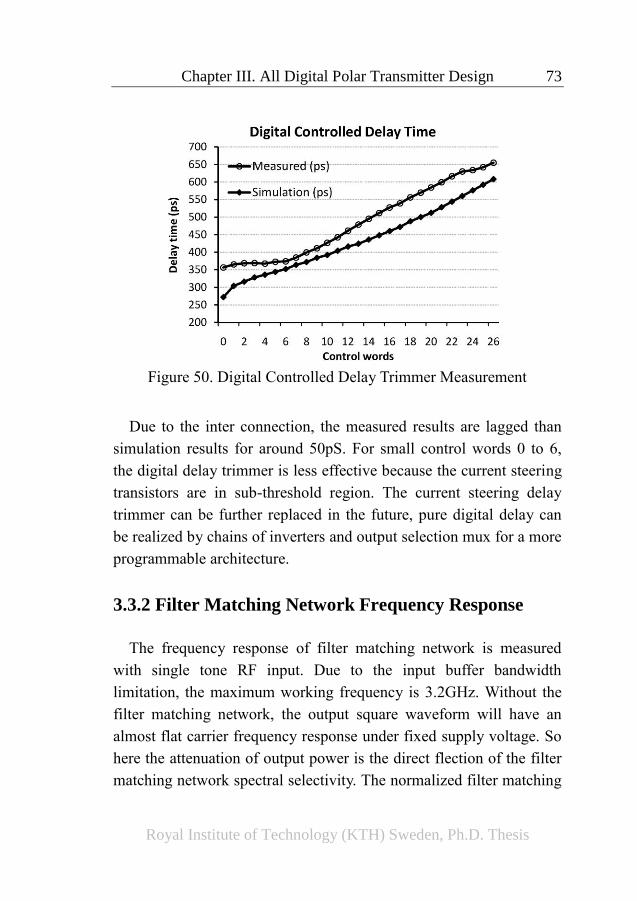
Chapter III. All Digital Polar Transmitter Design 73
Royal Institute of Technology (KTH) Sweden, Ph.D. Thesis
Figure 50. Digital Controlled Delay Trimmer Measurement
Due to the inter connection, the measured results are lagged than
simulation results for around 50pS. For small control words 0 to 6,
the digital delay trimmer is less effective because the current steering
transistors are in sub-threshold region. The current steering delay
trimmer can be further replaced in the future, pure digital delay can
be realized by chains of inverters and output selection mux for a more
programmable architecture.
3.3.2 Filter Matching Network Frequency Response
The frequency response of filter matching network is measured
with single tone RF input. Due to the input buffer bandwidth
limitation, the maximum working frequency is 3.2GHz. Without the
filter matching network, the output square waveform will have an
almost flat carrier frequency response under fixed supply voltage. So
here the attenuation of output power is the direct flection of the filter
matching network spectral selectivity. The normalized filter matching
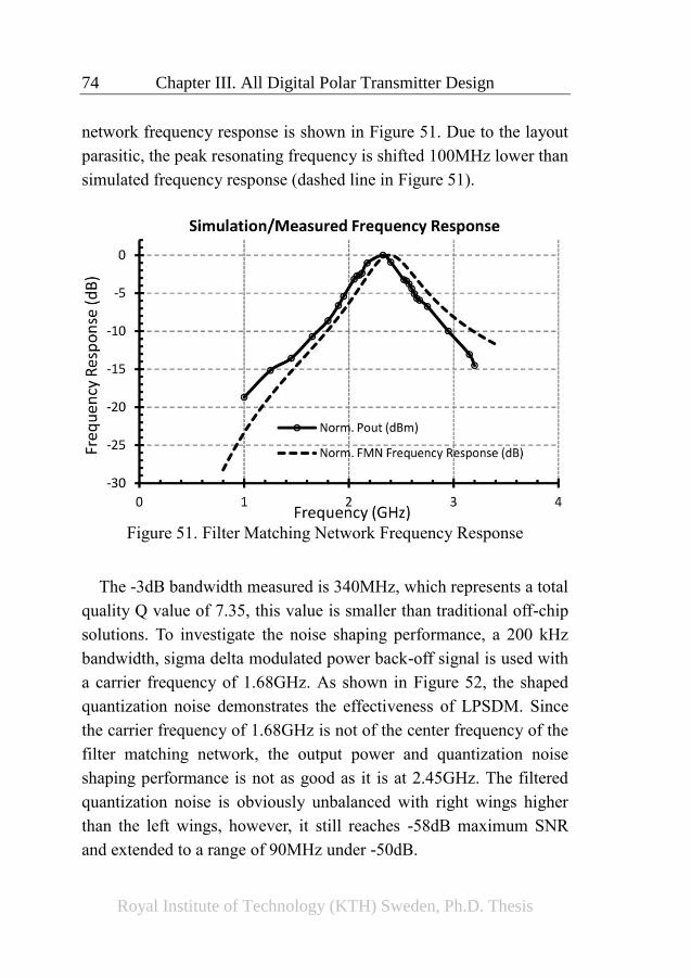
74 Chapter III. All Digital Polar Transmitter Design
Royal Institute of Technology (KTH) Sweden, Ph.D. Thesis
network frequency response is shown in Figure 51. Due to the layout
parasitic, the peak resonating frequency is shifted 100MHz lower than
simulated frequency response (dashed line in Figure 51).
Figure 51. Filter Matching Network Frequency Response
The -3dB bandwidth measured is 340MHz, which represents a total
quality Q value of 7.35, this value is smaller than traditional off-chip
solutions. To investigate the noise shaping performance, a 200 kHz
bandwidth, sigma delta modulated power back-off signal is used with
a carrier frequency of 1.68GHz. As shown in Figure 52, the shaped
quantization noise demonstrates the effectiveness of LPSDM. Since
the carrier frequency of 1.68GHz is not of the center frequency of the
filter matching network, the output power and quantization noise
shaping performance is not as good as it is at 2.45GHz. The filtered
quantization noise is obviously unbalanced with right wings higher
than the left wings, however, it still reaches -58dB maximum SNR
and extended to a range of 90MHz under -50dB.
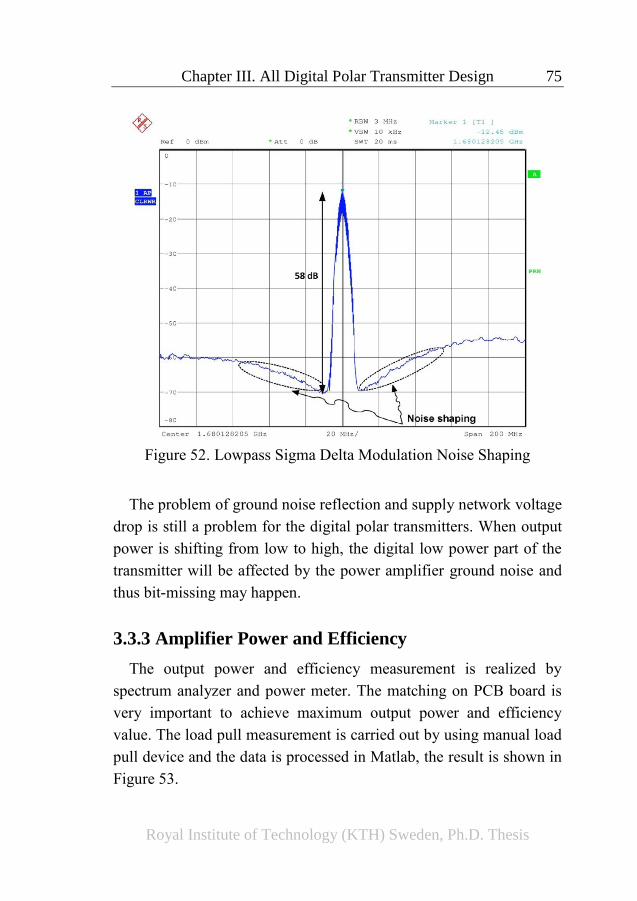
Chapter III. All Digital Polar Transmitter Design 75
Royal Institute of Technology (KTH) Sweden, Ph.D. Thesis
Figure 52. Lowpass Sigma Delta Modulation Noise Shaping
The problem of ground noise reflection and supply network voltage
drop is still a problem for the digital polar transmitters. When output
power is shifting from low to high, the digital low power part of the
transmitter will be affected by the power amplifier ground noise and
thus bit-missing may happen.
3.3.3 Amplifier Power and Efficiency
The output power and efficiency measurement is realized by
spectrum analyzer and power meter. The matching on PCB board is
very important to achieve maximum output power and efficiency
value. The load pull measurement is carried out by using manual load
pull device and the data is processed in Matlab, the result is shown in
Figure 53.
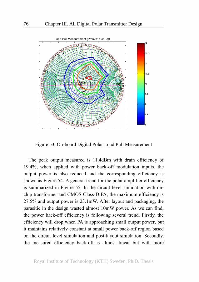
76 Chapter III. All Digital Polar Transmitter Design
Royal Institute of Technology (KTH) Sweden, Ph.D. Thesis
Figure 53. On-board Digital Polar Load Pull Measurement
The peak output measured is 11.4dBm with drain efficiency of
19.4%, when applied with power back-off modulation inputs, the
output power is also reduced and the corresponding efficiency is
shown as Figure 54. A general trend for the polar amplifier efficiency
is summarized in Figure 55. In the circuit level simulation with on-
chip transformer and CMOS Class-D PA, the maximum efficiency is
27.5% and output power is 23.1mW. After layout and packaging, the
parasitic in the design wasted almost 10mW power. As we can find,
the power back-off efficiency is following several trend. Firstly, the
efficiency will drop when PA is approaching small output power, but
it maintains relatively constant at small power back-off region based
on the circuit level simulation and post-layout simulation. Secondly,
the measured efficiency back-off is almost linear but with more
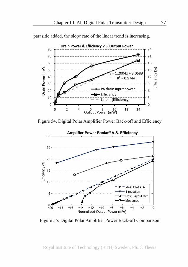
Chapter III. All Digital Polar Transmitter Design 77
Royal Institute of Technology (KTH) Sweden, Ph.D. Thesis
parasitic added, the slope rate of the linear trend is increasing.
Figure 54. Digital Polar Amplifier Power Back-off and Efficiency
Figure 55. Digital Polar Amplifier Power Back-off Comparison
78 Chapter III. All Digital Polar Transmitter Design
Royal Institute of Technology (KTH) Sweden, Ph.D. Thesis
Based on LPSDM algorithm, either a full cycle pulse or non will be
generated during a carrier frequency cycle. The SDM modulation is
charging sliced power portion into the filter matching network and the
amount is defined by the oversampling ratio. The discrete portion of
power is generated by the class-D amplifier and averaged by the filter
matching network for a smooth output. Based on the H-Bridge
architecture and the filter matching network, when output power is
low, the corresponding SDM envelope pulse number will also
decrease. In order to maintain the resonating between the primary and
secondary stage of the transformer in filter matching network, the H-
Bridge will provide a grounding path for the current. So the averaged
impedance of the transformer is varying with the output power level.
For example, assuming the oversampling ratio is 10. When it is a
full swing SDM envelope output case, 10 portions of power will be
injected and the transformer consumes 0.1 portions every cycle. The
total efficiency will be 90%. While in 10% swing case, only 1 portion
of power is injected and the output has to sustain for 10 cycles to
average the output, the accumulated transformer lost will be over 0.8
portions and the total efficiency will be lower than 20%. A more
detailed analysis on the time amplitude related impedance is given in
Append II.
Based on this observation, a simplified model is built and the
corresponding simulation is compared with measured results shown
in Figure 56. It can be seen that the simulation results are similar to
the measurement results. In order to maintain power efficiency level,
large grounding NMOS transistor should be used but the driving
power loss will increase, this is also a trade-off in the class-D PA
optimization.
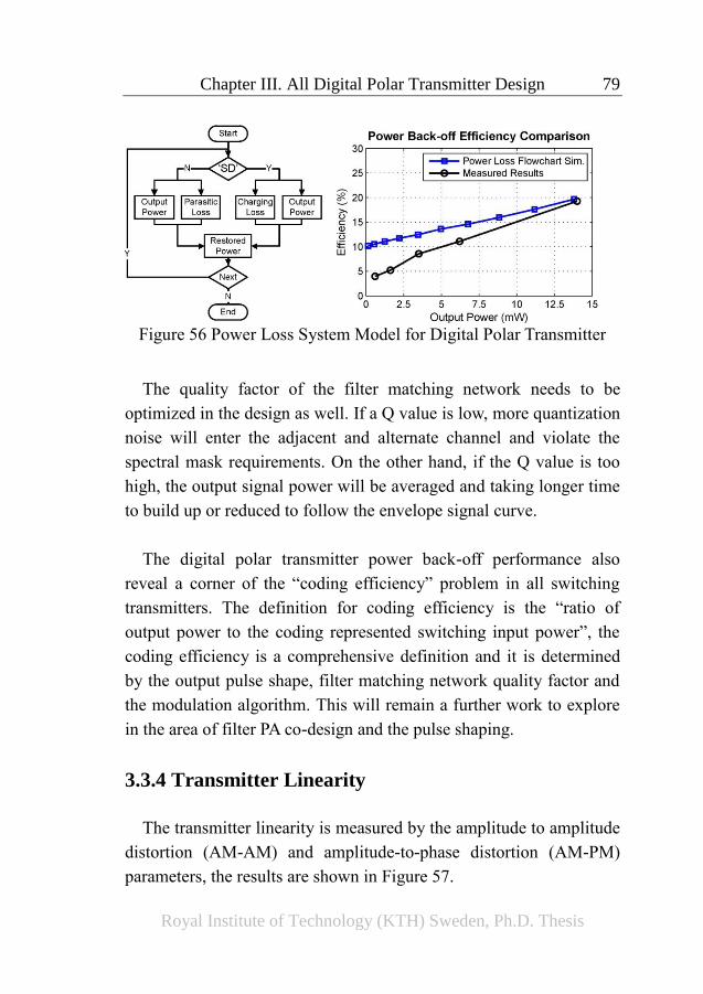
Chapter III. All Digital Polar Transmitter Design 79
Royal Institute of Technology (KTH) Sweden, Ph.D. Thesis
Figure 56 Power Loss System Model for Digital Polar Transmitter
The quality factor of the filter matching network needs to be
optimized in the design as well. If a Q value is low, more quantization
noise will enter the adjacent and alternate channel and violate the
spectral mask requirements. On the other hand, if the Q value is too
high, the output signal power will be averaged and taking longer time
to build up or reduced to follow the envelope signal curve.
The digital polar transmitter power back-off performance also
reveal a corner of the “coding efficiency” problem in all switching
transmitters. The definition for coding efficiency is the “ratio of
output power to the coding represented switching input power”, the
coding efficiency is a comprehensive definition and it is determined
by the output pulse shape, filter matching network quality factor and
the modulation algorithm. This will remain a further work to explore
in the area of filter PA co-design and the pulse shaping.
3.3.4 Transmitter Linearity
The transmitter linearity is measured by the amplitude to amplitude
distortion (AM-AM) and amplitude-to-phase distortion (AM-PM)
parameters, the results are shown in Figure 57.
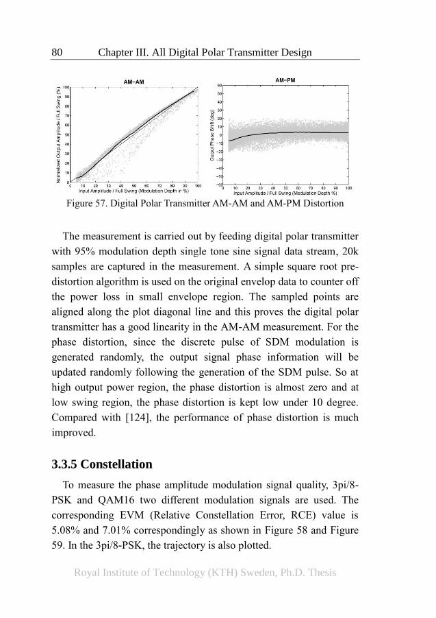
80 Chapter III. All Digital Polar Transmitter Design
Royal Institute of Technology (KTH) Sweden, Ph.D. Thesis
Figure 57. Digital Polar Transmitter AM-AM and AM-PM Distortion
The measurement is carried out by feeding digital polar transmitter
with 95% modulation depth single tone sine signal data stream, 20k
samples are captured in the measurement. A simple square root pre-
distortion algorithm is used on the original envelop data to counter off
the power loss in small envelope region. The sampled points are
aligned along the plot diagonal line and this proves the digital polar
transmitter has a good linearity in the AM-AM measurement. For the
phase distortion, since the discrete pulse of SDM modulation is
generated randomly, the output signal phase information will be
updated randomly following the generation of the SDM pulse. So at
high output power region, the phase distortion is almost zero and at
low swing region, the phase distortion is kept low under 10 degree.
Compared with [124], the performance of phase distortion is much
improved.
3.3.5 Constellation
To measure the phase amplitude modulation signal quality, 3pi/8-
PSK and QAM16 two different modulation signals are used. The
corresponding EVM (Relative Constellation Error, RCE) value is
5.08% and 7.01% correspondingly as shown in Figure 58 and Figure
59. In the 3pi/8-PSK, the trajectory is also plotted.

Chapter III. All Digital Polar Transmitter Design 81
Royal Institute of Technology (KTH) Sweden, Ph.D. Thesis
Figure 58. Digital Polar Transmitter 3Pi/8PSK Modulation Constellation
Figure 59. Digital Polar Transmitter QAM16 Modulation Constellation
UNCAL
Ref LvlRef Lvl
-15 dBm
Ref Lvl
-15 dBm
Ref Lvl
-15 dBm
Ref Lvl
-15 dBm
TRG
CF 1.68 GHz
SR 500 kHzSR 500 kHz
Symbol/Errors
Demod 16QAMDemod 16QAM
LNLN
B
UNCAL
Ref LvlRef Lvl
-15 dBm
Ref Lvl
-15 dBm
Ref Lvl
-15 dBm
Ref Lvl
-15 dBm
TRG
CF 1.68 GHz
SR 500 kHzSR 500 kHz
Meas Signal
ConstellationConstellation
Demod 16QAMDemod 16QAM
IMAG
T1
A
LNLN
EXT
SGL
SGL
-1
1
1
Marker 1 [T1] 0.00 sym
Magnitude 970.579 m
Phase 43.20 deg
Symbol Table
0 00001100 10100111 00100001 01001001 11101011
40 01100101 10001101 11110011 00001100 11110011
80 00001100 10100111 00100001 01001001 11101011
Error Summary
Error Vector Mag 7.01 % rms 12.62 % Pk at sym 76
Magnitude Error 4.94 % rms 8.48 % Pk at sym 107
Phase Error 3.52 deg rms 9.45 deg Pk at sym 42
Freq Error -28.25 Hz -28.25 Hz Pk
Amplitude Droop 8.20 dB/sym Rho Factor 0.9890
IQ Offset 0.96 % IQ Imbalance 0.65 %
Date: 7.DEC.2011 16:06:10
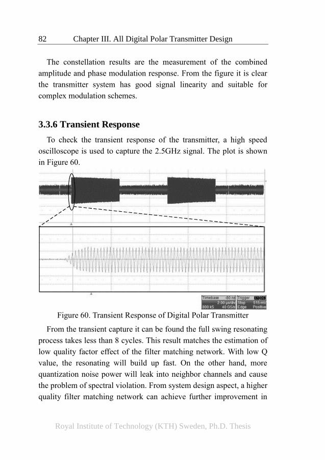
82 Chapter III. All Digital Polar Transmitter Design
Royal Institute of Technology (KTH) Sweden, Ph.D. Thesis
The constellation results are the measurement of the combined
amplitude and phase modulation response. From the figure it is clear
the transmitter system has good signal linearity and suitable for
complex modulation schemes.
3.3.6 Transient Response
To check the transient response of the transmitter, a high speed
oscilloscope is used to capture the 2.5GHz signal. The plot is shown
in Figure 60.
Figure 60. Transient Response of Digital Polar Transmitter
From the transient capture it can be found the full swing resonating
process takes less than 8 cycles. This result matches the estimation of
low quality factor effect of the filter matching network. With low Q
value, the resonating will build up fast. On the other hand, more
quantization noise power will leak into neighbor channels and cause
the problem of spectral violation. From system design aspect, a higher
quality filter matching network can achieve further improvement in
Chapter III. All Digital Polar Transmitter Design 83
Royal Institute of Technology (KTH) Sweden, Ph.D. Thesis
output signal purity.
3.4 All Digital Polar Transmitter Design
Summary
In this chapter, the systematic analysis, design and measurement of
the digital polar transmitter is carried out. By exploring the polar
architecture and developing models to verify the idea, polar
transmitter in digital style has been proved to have satisfactory
linearity and simple architecture. Possible modulation algorithms are
evaluated and phase synchronized RF LPSDM algorithm is chosen to
realize a fully digital polar transmitter. In order to use the CMOS
process scaling advantages, the system is designed in UMC90nm
process with on-chip filter matching network. The output power and
efficiency performance is measured and possible power loss
mechanism is detected.
This chapter also gives the answer to the second question raised in
the beginning. It is absolutely possible to take the fast switching
advantage of the CMOS process to create a fully digital polar
transmitter. And the phase synchronized RF LPSDM algorithm is
suitable to reduce the switching loss to achieve satisfactory linearity.
The output power and efficiency performance revealed the design
limitation in low supply voltage process and further improvements
can be made.
84 Chapter III. All Digital Polar Transmitter Design
Royal Institute of Technology (KTH) Sweden, Ph.D. Thesis
(This page is intentionally left blank.)
Royal Institute of Technology (KTH) Sweden, Ph.D. Thesis
Chapter IV. SDR Implementation
for Radio Frequency Identification
(RFID) Technology
The Radio Frequency Identification (RFID) technology is a low
power, low data rate, shot to medium range wireless communication
gaining more and more attention recent years. The demands of global
merchandise location tracking, item quality control and product
promotion stimulate the development of RFID technology and the
growth of the market will last for the coming decade. To keep this
trend, the RFID system has to overcome many design challenges to
reduce the manufacture cost as well as be more efficient in power
consumption. The implementation of RFID embedded mobile phone
also propels a ’green’ RFID system for long battery life applications.
In different system design hierarchies, progress can be made to realize
the targeted economic RFID readers and tags.
In this chapter, a SDR based RFID system is proposed based on
previous digital polar transmitter architecture and the flash ADC. The
feature of RFID in UHF band provided a very suitable targeting
application for the verification of TX/RX blocks introduced above. In
the work [P4], the UHF RFID transmitter system is simulated totally
by digital programming. FPGA platform is used to prototype the
design to show the whole system can be realized in SDR format.
Based on the results, further improvement on the digital polar
transmitter is triggered and they are providing a direction to realize
other complex wireless communication.
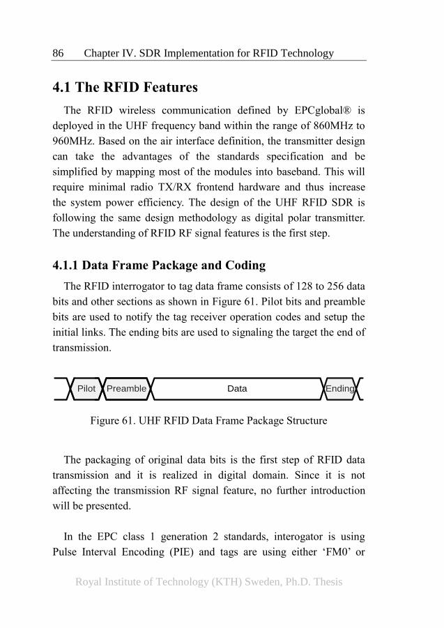
86 Chapter IV. SDR Implementation for RFID Technology
Royal Institute of Technology (KTH) Sweden, Ph.D. Thesis
4.1 The RFID Features
The RFID wireless communication defined by EPCglobal® is
deployed in the UHF frequency band within the range of 860MHz to
960MHz. Based on the air interface definition, the transmitter design
can take the advantages of the standards specification and be
simplified by mapping most of the modules into baseband. This will
require minimal radio TX/RX frontend hardware and thus increase
the system power efficiency. The design of the UHF RFID SDR is
following the same design methodology as digital polar transmitter.
The understanding of RFID RF signal features is the first step.
4.1.1 Data Frame Package and Coding
The RFID interrogator to tag data frame consists of 128 to 256 data
bits and other sections as shown in Figure 61. Pilot bits and preamble
bits are used to notify the tag receiver operation codes and setup the
initial links. The ending bits are used to signaling the target the end of
transmission.
Preamble Data EndingPilot
Figure 61. UHF RFID Data Frame Package Structure
The packaging of original data bits is the first step of RFID data
transmission and it is realized in digital domain. Since it is not
affecting the transmission RF signal feature, no further introduction
will be presented.
In the EPC class 1 generation 2 standards, interogator is using
Pulse Interval Encoding (PIE) and tags are using either ‘FM0’ or
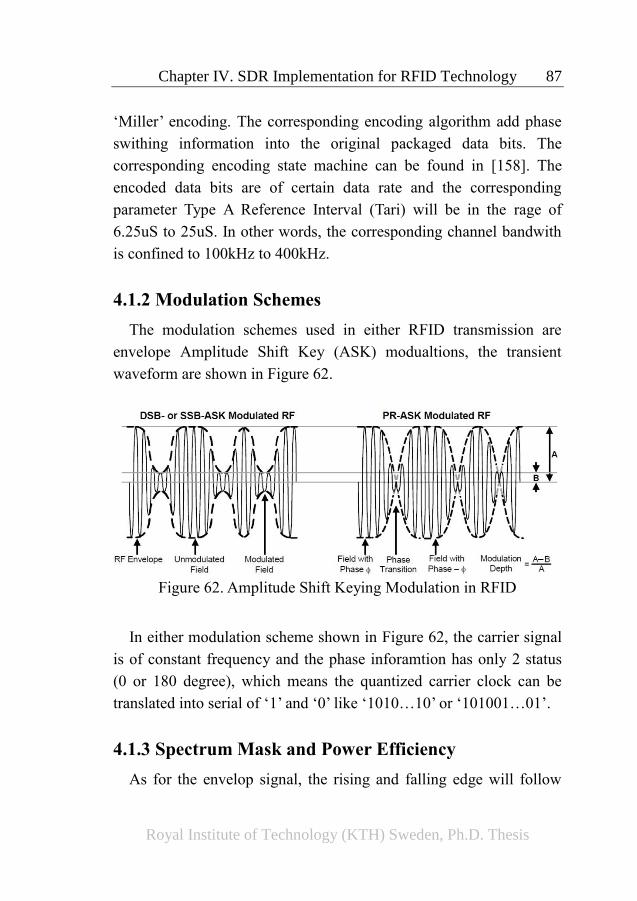
Chapter IV. SDR Implementation for RFID Technology 87
Royal Institute of Technology (KTH) Sweden, Ph.D. Thesis
‘Miller’ encoding. The corresponding encoding algorithm add phase
swithing information into the original packaged data bits. The
corresponding encoding state machine can be found in [158]. The
encoded data bits are of certain data rate and the corresponding
parameter Type A Reference Interval (Tari) will be in the rage of
6.25uS to 25uS. In other words, the corresponding channel bandwith
is confined to 100kHz to 400kHz.
4.1.2 Modulation Schemes
The modulation schemes used in either RFID transmission are
envelope Amplitude Shift Key (ASK) modualtions, the transient
waveform are shown in Figure 62.
Figure 62. Amplitude Shift Keying Modulation in RFID
In either modulation scheme shown in Figure 62, the carrier signal
is of constant frequency and the phase inforamtion has only 2 status
(0 or 180 degree), which means the quantized carrier clock can be
translated into serial of ‘1’ and ‘0’ like ‘1010…10’ or ‘101001…01’.
4.1.3 Spectrum Mask and Power Efficiency
As for the envelop signal, the rising and falling edge will follow
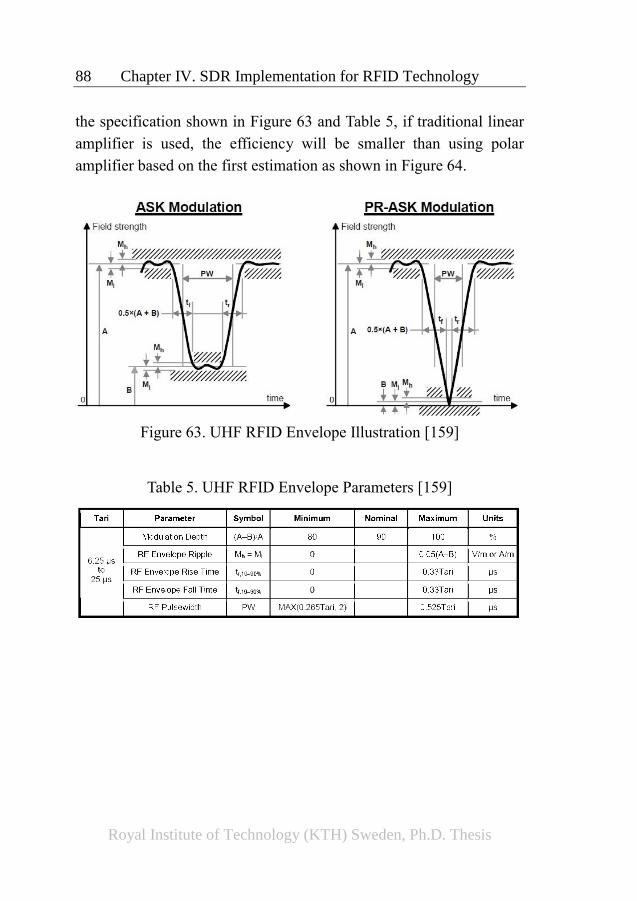
88 Chapter IV. SDR Implementation for RFID Technology
Royal Institute of Technology (KTH) Sweden, Ph.D. Thesis
the specification shown in Figure 63 and Table 5, if traditional linear
amplifier is used, the efficiency will be smaller than using polar
amplifier based on the first estimation as shown in Figure 64.
Figure 63. UHF RFID Envelope Illustration [159]
Table 5. UHF RFID Envelope Parameters [159]
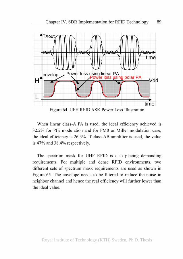
Chapter IV. SDR Implementation for RFID Technology 89
Royal Institute of Technology (KTH) Sweden, Ph.D. Thesis
Vdd
Power loss using linear PA Power loss using polar PA
Figure 64. UFH RFID ASK Power Loss Illustration
When linear class-A PA is used, the ideal efficiency achieved is
32.2% for PIE modulation and for FM0 or Miller modulation case,
the ideal efficiency is 26.3%. If class-AB amplifier is used, the value
is 47% and 38.4% respectively.
The spectrum mask for UHF RFID is also placing demanding
requirements. For multiple and dense RFID environments, two
different sets of spectrum mask requirements are used as shown in
Figure 65. The envelope needs to be filtered to reduce the noise in
neighbor channel and hence the real efficiency will further lower than
the ideal value.
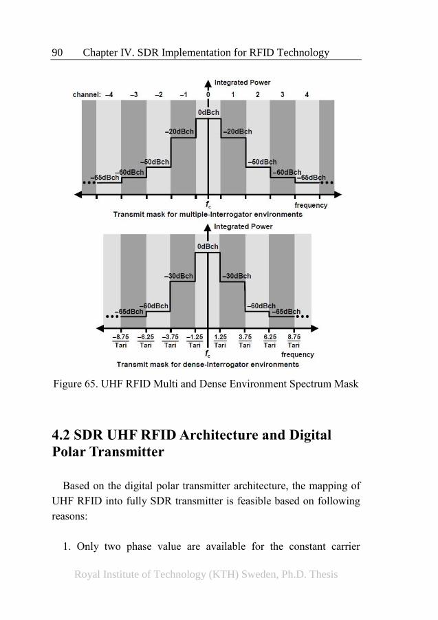
90 Chapter IV. SDR Implementation for RFID Technology
Royal Institute of Technology (KTH) Sweden, Ph.D. Thesis
Figure 65. UHF RFID Multi and Dense Environment Spectrum Mask
4.2 SDR UHF RFID Architecture and Digital
Polar Transmitter
Based on the digital polar transmitter architecture, the mapping of
UHF RFID into fully SDR transmitter is feasible based on following
reasons:
1. Only two phase value are available for the constant carrier
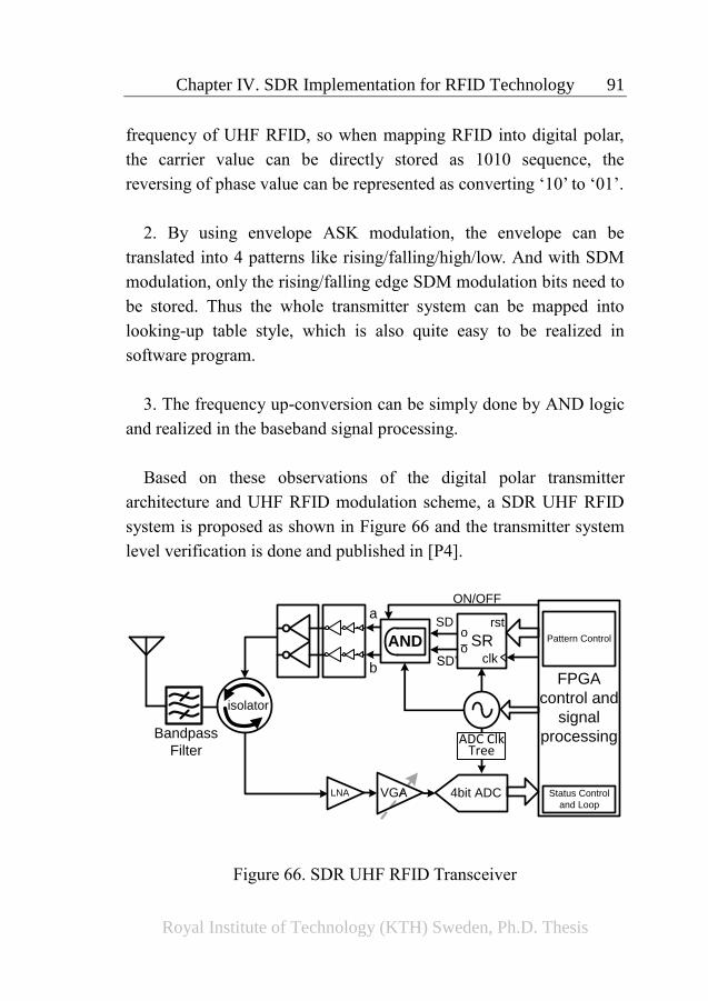
Chapter IV. SDR Implementation for RFID Technology 91
Royal Institute of Technology (KTH) Sweden, Ph.D. Thesis
frequency of UHF RFID, so when mapping RFID into digital polar,
the carrier value can be directly stored as 1010 sequence, the
reversing of phase value can be represented as converting ‘10’ to ‘01’.
2. By using envelope ASK modulation, the envelope can be
translated into 4 patterns like rising/falling/high/low. And with SDM
modulation, only the rising/falling edge SDM modulation bits need to
be stored. Thus the whole transmitter system can be mapped into
looking-up table style, which is also quite easy to be realized in
software program.
3. The frequency up-conversion can be simply done by AND logic
and realized in the baseband signal processing.
Based on these observations of the digital polar transmitter
architecture and UHF RFID modulation scheme, a SDR UHF RFID
system is proposed as shown in Figure 66 and the transmitter system
level verification is done and published in [P4].
LNA 4bit ADCVGA
SDa
b
AND
SD’
SRclk
o
o
rst
isolator
ADC Clk Tree
FPGA
control and
signal
processing
Pattern Control
Status Control
and Loop
ON/OFF
Bandpass
Filter
Figure 66. SDR UHF RFID Transceiver
92 Chapter IV. SDR Implementation for RFID Technology
Royal Institute of Technology (KTH) Sweden, Ph.D. Thesis
Figure 67. Digital Polar UHF RFID Transmitter Spectrum Mask
In the [158][[159], the transmitter envelope rising and falling edge
timing requirements are investigated as shown in Figure 67, to meet
the dense tag environment spectrum mask requirements, the
minimum rising/falling edge timing value is 0.22Tari. The
corresponding ideal system efficiency is also measured and over 77%
efficiency can be achieved.
4.3 FPGA Programmed SDR UHF RFID
To further prove the feasibility of SDR UHF RFID transmitter, the
system is programmed in VHDL language and downloaded in to
SP605 Xilinx® FPGA for the verification. The corresponding output
spectrum is shown in Figure 68.
Chapter IV. SDR Implementation for RFID Technology 93
Royal Institute of Technology (KTH) Sweden, Ph.D. Thesis
Ref -10 dBm Att 15 dB
AVG
A
IFOVL
Center 800 MHz Span 2 MHz200 kHz/
*RBW 50 kHz
VBW 200 kHz
SWT 10 ms
1 SA
PRN
-110
-100
-90
-80
-70
-60
-50
-40
-30
-20
-10
SWP 100 of 100
1
Marker 1 [T1 ]
-23.87 dBm
800.136000000 MHz
2
Delta 2 [T1 ]
-23.72 dB
321.600000000 kHz
3
Delta 3 [T1 ]
-42.13 dB
660.800000000 kHz
Date: 20.AUG.2011 21:54:58
Channel 0
Channel 1
Channel 2
NRZ-noise
Figure 68. Digital UHF RFID FPGA Transmitter
Due to the FPGA differential output configuration, the FPGA has
non-return-to-zero (NRZ) signaling output. Thus the spectrum is
different from Figure 67 with higher carrier leakage. And since on
board DCDC voltage converter module is also fixed on the FPGA to
convert 12V to 5V IO voltage, the noise floor of the output signal is
higher than the -65dBc/kHz in the measurement.
However, this experiment proved the hardware can be programmed
into UHF RFID transmitter by implementing the digital polar
transmitter algorithm. As a part of the SDR system design, with better
supply noise filtering, a fully digital polar transmitter can be realized
94 Chapter IV. SDR Implementation for RFID Technology
Royal Institute of Technology (KTH) Sweden, Ph.D. Thesis
and the integration level with digital part is high.
4.4 Conclusion on SDR UHF RFID Digital Polar
Transmitter
In this chapter, a SDR UHF RFID digital polar transmitter is
verified by system level simulation and designed in the VHDL
language. The system level simulation results provide important
RFID envelop timing requirements and power efficiency
performance. In order to map the system into digital polar transmitter
architecture with more programmable feature, the algorithm
developed is designed in the VHDL codes and this provides an
example for further application of the architecture for other similar
wireless communication standards.
The practical results demonstrated in FPGA board also answered
the third question raised in the beginning. The SDR solution is
possible to be found for other wireless communication standards as
well. The UHF RFID is a specific application since it has limited
phase information in the transmitted signal. For other wireless
standards embedded with phase modulation scheme, the problem can
be solved by improve the digital phase modulator part and it is also
possible to be realized in pure digital process and programmable
style.
Royal Institute of Technology (KTH) Sweden, Ph.D. Thesis
Chapter V. Summary of Thesis and
Future Works
In the previous chapters, the investigation on the SDR architecture
[P1] and transmitter topology selection are performed, the
comparison on different transmitter architectures shows that the polar
transmitter has the advantages in power efficiency and possibility in
the digital realization [P2]. Based on the system level simulation, the
digital polar transmitter is designed under 90nm CMOS process as
introduced in Section 3.2 [P3]. The system performance parameters
like frequency response, output power and efficiency are measured. A
peak output power of 11.4dBm with 19.4% efficiency is achieved
with single 1.0V supply voltage. Due to the use of switching
amplifier, transient phase and amplitude serial input data
measurement skills are developed. The system achieved EVM value
of 5.08% and 7.01% for 3pi/8-PSK and QAM16 modulation
respectively. The measurement results proved the system linearity and
revealed the power back-off efficiency characteristics under low
supply voltage, low Q devices environment [P6][P5]. As a whole
system solution, the collaborated work [P7] provided a more
complete integrated digital solution.
To further explore the potential of digital polar transmitter integrity
into SDR system, UHF RFID standard is used as specific example to
implement the digital design algorithm [P4]. By mapping and
translating the UHF RFID output signal into digital polar transmitter
blocks, a fully software (VHDL) design is realized and programmed
into FPGA for comparison with system level simulation. The results
prove the feasibility of the design methodology and also pointed out
the hardware requirements.
96 Chapter IV. SDR Implementation for RFID Technology
Royal Institute of Technology (KTH) Sweden, Ph.D. Thesis
Future Works
Based on the digital polar amplifier and UHF RFID design, the
future work will be the power and efficiency improvement on the
switching power amplifier. As it is estimated that the power back-off
trend is defined by the transistor internal impedance and the filter
matching network quality factor, a co-design of the last stage will be
the main research direction in the further work.
In the SDR UHF RFID direction, after understanding the FPGA
limitations, a customized ASIC design based on the VHDL codes will
be arranged. The timing sequence of design will be carefully
manipulated to verify the concept of SDR UHF RFID and a complete
transceiver solution will be targeted.
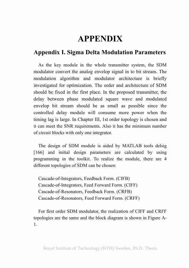
Royal Institute of Technology (KTH) Sweden, Ph.D. Thesis
APPENDIX
Appendix I. Sigma Delta Modulation Parameters
As the key module in the whole transmitter system, the SDM
modulator convert the analog envelop signal in to bit stream. The
modulation algorithm and modulator architecture is briefly
investigated for optimization. The order and architecture of SDM
should be fixed in the first place. In the proposed transmitter, the
delay between phase modulated square wave and modulated
envelop bit stream should be as small as possible since the
controlled delay module will consume more power when the
timing lag is large. In Chapter III, 1st order topology is chosen and
it can meet the SNR requirements. Also it has the minimum number
of circuit blocks with only one integrator.
The design of SDM module is aided by MATLAB tools delsig
[166] and initial design parameters are calculated by using
programming in the toolkit. To realize the module, there are 4
different topologies of SDM can be chosen:
Cascade-of-Integrators, Feedback Form. (CIFB)
Cascade-of-Integrators, Feed Forward Form. (CIFF)
Cascade-of-Resonators, Feedback Form. (CRFB)
Cascade-of-Resonators, Feed Forward Form. (CRFF)
For first order SDM modulator, the realization of CIFF and CRFF
topologies are the same and the block diagram is shown in Figure A-
1.
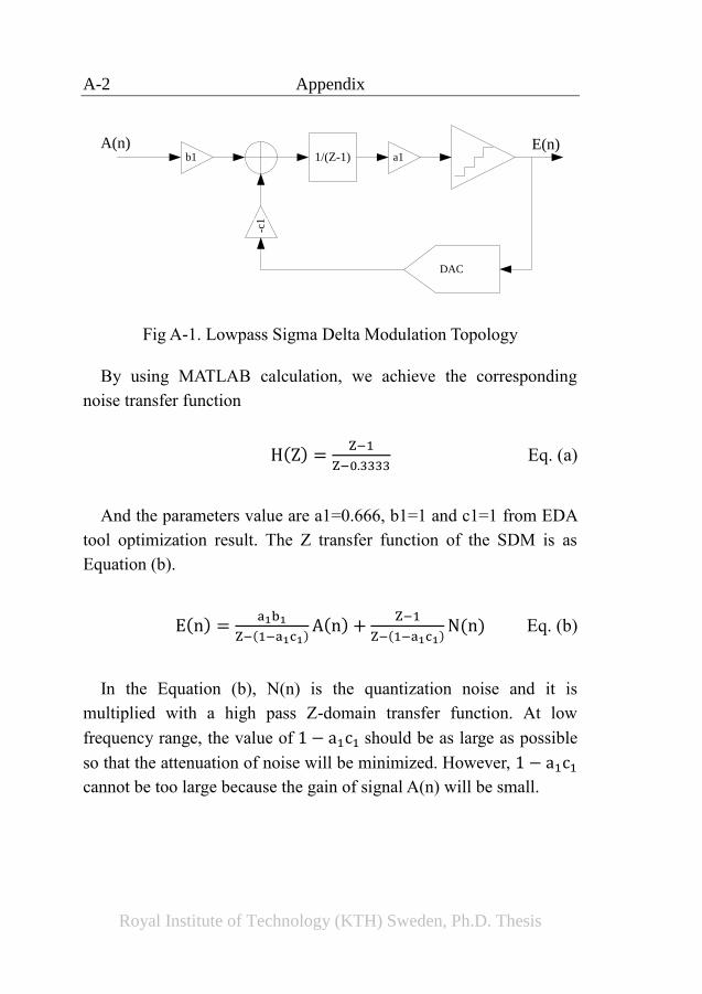
A-2 Appendix
Royal Institute of Technology (KTH) Sweden, Ph.D. Thesis
b1 1/(Z-1) a1
-c1
DAC
A(n) E(n)
Fig A-1. Lowpass Sigma Delta Modulation Topology
By using MATLAB calculation, we achieve the corresponding
noise transfer function
H(Z) =Z−1
Z−0.3333 Eq. (a)
And the parameters value are a1=0.666, b1=1 and c1=1 from EDA
tool optimization result. The Z transfer function of the SDM is as
Equation (b).
E(n) =a1b1
Z−(1−a1c1)A(n) +
Z−1
Z−(1−a1c1)N(n) Eq. (b)
In the Equation (b), N(n) is the quantization noise and it is
multiplied with a high pass Z-domain transfer function. At low
frequency range, the value of 1 − a1c1 should be as large as possible
so that the attenuation of noise will be minimized. However, 1 − a1c1
cannot be too large because the gain of signal A(n) will be small.
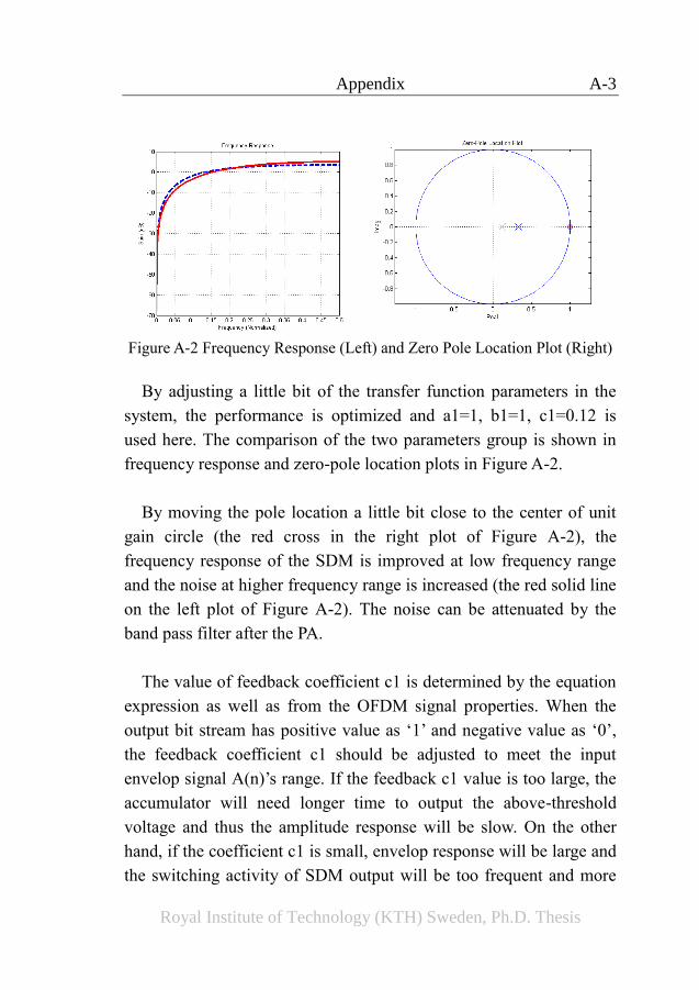
Appendix A-3
Royal Institute of Technology (KTH) Sweden, Ph.D. Thesis
Figure A-2 Frequency Response (Left) and Zero Pole Location Plot (Right)
By adjusting a little bit of the transfer function parameters in the
system, the performance is optimized and a1=1, b1=1, c1=0.12 is
used here. The comparison of the two parameters group is shown in
frequency response and zero-pole location plots in Figure A-2.
By moving the pole location a little bit close to the center of unit
gain circle (the red cross in the right plot of Figure A-2), the
frequency response of the SDM is improved at low frequency range
and the noise at higher frequency range is increased (the red solid line
on the left plot of Figure A-2). The noise can be attenuated by the
band pass filter after the PA.
The value of feedback coefficient c1 is determined by the equation
expression as well as from the OFDM signal properties. When the
output bit stream has positive value as ‘1’ and negative value as ‘0’,
the feedback coefficient c1 should be adjusted to meet the input
envelop signal A(n)’s range. If the feedback c1 value is too large, the
accumulator will need longer time to output the above-threshold
voltage and thus the amplitude response will be slow. On the other
hand, if the coefficient c1 is small, envelop response will be large and
the switching activity of SDM output will be too frequent and more
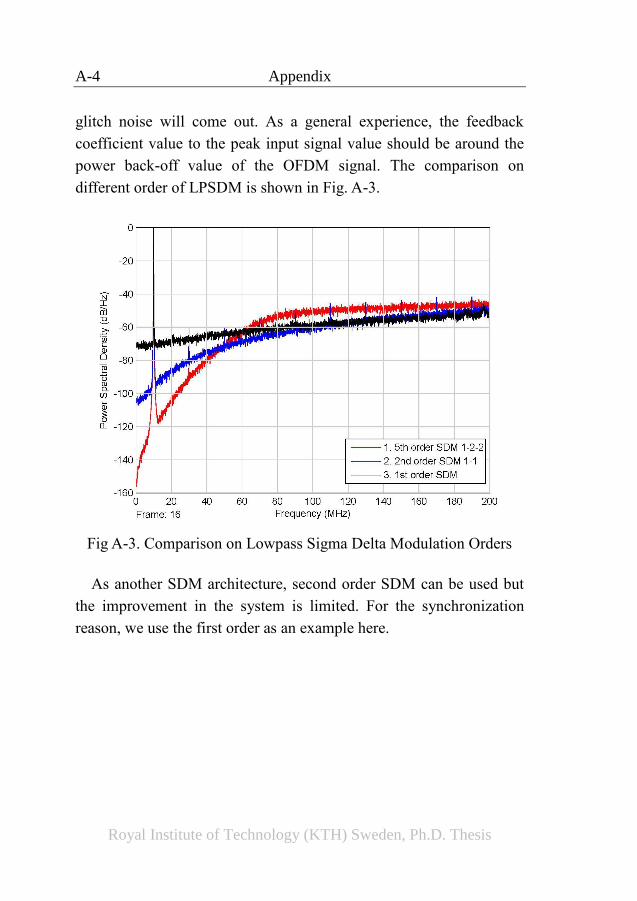
A-4 Appendix
Royal Institute of Technology (KTH) Sweden, Ph.D. Thesis
glitch noise will come out. As a general experience, the feedback
coefficient value to the peak input signal value should be around the
power back-off value of the OFDM signal. The comparison on
different order of LPSDM is shown in Fig. A-3.
Fig A-3. Comparison on Lowpass Sigma Delta Modulation Orders
As another SDM architecture, second order SDM can be used but
the improvement in the system is limited. For the synchronization
reason, we use the first order as an example here.
Appendix A-5
Royal Institute of Technology (KTH) Sweden, Ph.D. Thesis
Appendix II. CMOS H-Bridge PA Power Loss
Mechanism
The CMOS process is the foundation of contemporary integration
circuit system design and the carrier of wireless communication
technology. Due to the process scaling, CMOS transistor can be
operated at tens of Giga-Hertz frequency range and it has already
been the bricks for radio frequency system design. In this work, the
CMOS transistors are also used to design the power amplifier for
fully integration purpose. In the sub-micron process, the supply
voltage is shrinking to 1V range, this brings the problem of small
voltage headroom and large current density if high output power is
required. In order to carry out successful digital polar transmitter
design especially CMOS power amplifier design, the basics of
CMOS process is of must-known from the start.
AII-1. Shockley square law model
The classic model used in the CMOS design for decades is the
Shockley square law model developed by William Shockley and it
is irritated in many literatures. However, this model is suitable for
MOS transistors with channel length larger than 1um. For sub-
micron devices, the square law model can no longer sustain the
accurate prediction of transistor performance due to the velocity
saturation of the carriers. An extension model called ‘Alpha Law’
model is used [155] to solve this problem and it can give more
accurate predictions of transistor performance. To compare the
difference between two models, equations are listed below.
The threshold voltage is defined by equation Eq. (c)
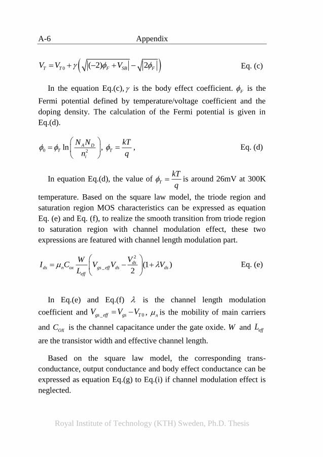
A-6 Appendix
Royal Institute of Technology (KTH) Sweden, Ph.D. Thesis
0 ( 2) 2T T F SB FV V V Eq. (c)
In the equation Eq.(c), is the body effect coefficient. F is the
Fermi potential defined by temperature/voltage coefficient and the
doping density. The calculation of the Fermi potential is given in
Eq.(d).
0 2ln A D
T
i
N N
n
, T
kT
q , Eq. (d)
In equation Eq.(d), the value of T
kT
q is around 26mV at 300K
temperature. Based on the square law model, the triode region and
saturation region MOS characteristics can be expressed as equation
Eq. (e) and Eq. (f), to realize the smooth transition from triode region
to saturation region with channel modulation effect, these two
expressions are featured with channel length modulation part.
2
_ (1 )2
dsds n ox gs eff ds ds
eff
VWI C V V V
L
Eq. (e)
In Eq.(e) and Eq.(f) is the channel length modulation
coefficient and _ 0gs eff gs TV V V , n is the mobility of main carriers
and OXC is the channel capacitance under the gate oxide. W and effL
are the transistor width and effective channel length.
Based on the square law model, the corresponding trans-
conductance, output conductance and body effect conductance can be
expressed as equation Eq.(g) to Eq.(i) if channel modulation effect is
neglected.
Appendix A-7
Royal Institute of Technology (KTH) Sweden, Ph.D. Thesis
_
2 2ds ox dsm
gs eff eff
I C WIg
V L
,
Eq. (g)
2
_2
oxds gs eff ds
eff
C Wg V I
L
, Eq. (h)
02
mmb
SB
gg
V
,
Eq. (i)
However, due to the velocity saturation of the carrier in the
inversed channel, for sub-micron devices, square law is no longer
accurate to describe the I-V curve in the real measurement. Alpha law
is used here for the prediction of operation points and transistor size
that should be used in the design.
AII-2. Alpha Law expression for UMC 90nm Process
The corresponding alpha law or so called ‘alpha power law’
expression is given as equation Eq.(j).
0
0
1 ( )geff ds geff ds geff gs T
eff
ds
geff ds ds ds geff gs T
eff
Wk V V V V V V V
LI
Wk V V V V V V V
L
Eq. (j)
In Eq. (j), a is the alpha law coefficient It is about 1.50~1.54 in
the 90nm SPLVT process, by using curve fitting algorithm and
parameter extraction, corresponding value is extracted as follows, and
the comparison between fitting model curve and real transistor
simulation curve (Width=1um, Length=80nm) is shown in Figure A-4.
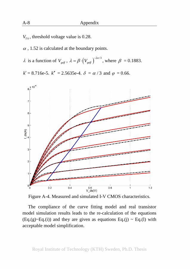
A-8 Appendix
Royal Institute of Technology (KTH) Sweden, Ph.D. Thesis
0TV , threshold voltage value is 0.28.
, 1.52 is calculated at the boundary points.
is a function of geffV ,
2 /3
geffV
, where = 0.1883.
k = 8.716e-5. k = 2.5635e-4. = / 3 and = 0.66.
Figure A-4. Measured and simulated I-V CMOS characteristics.
The compliance of the curve fitting model and real transistor
model simulation results leads to the re-calculation of the equations
(Eq.(g)~Eq.(i)) and they are given as equations Eq.(j) ~ Eq.(l) with
acceptable model simplification.
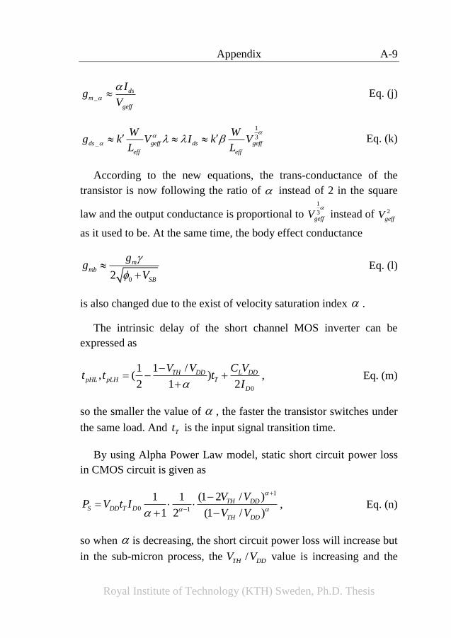
Appendix A-9
Royal Institute of Technology (KTH) Sweden, Ph.D. Thesis
_
ds
m
geff
Ig
V
Eq. (j)
1
3_
ds geff ds geff
eff eff
W Wg k V I k V
L L Eq. (k)
According to the new equations, the trans-conductance of the
transistor is now following the ratio of instead of 2 in the square
law and the output conductance is proportional to 1
3
geffV instead of 2
geffV
as it used to be. At the same time, the body effect conductance
02
mmb
SB
gg
V
Eq. (l)
is also changed due to the exist of velocity saturation index .
The intrinsic delay of the short channel MOS inverter can be
expressed as
0
1 /1, ( )
2 1 2
TH DD L DDpHL pLH T
D
V V C Vt t t
I
, Eq. (m)
so the smaller the value of , the faster the transistor switches under
the same load. And Tt is the input signal transition time.
By using Alpha Power Law model, static short circuit power loss
in CMOS circuit is given as
1
0 1
(1 2 / )1 1
1 2 (1 / )
TH DDS DD T D
TH DD
V VP V t I
V V
, Eq. (n)
so when is decreasing, the short circuit power loss will increase but
in the sub-micron process, the /TH DDV V value is increasing and the
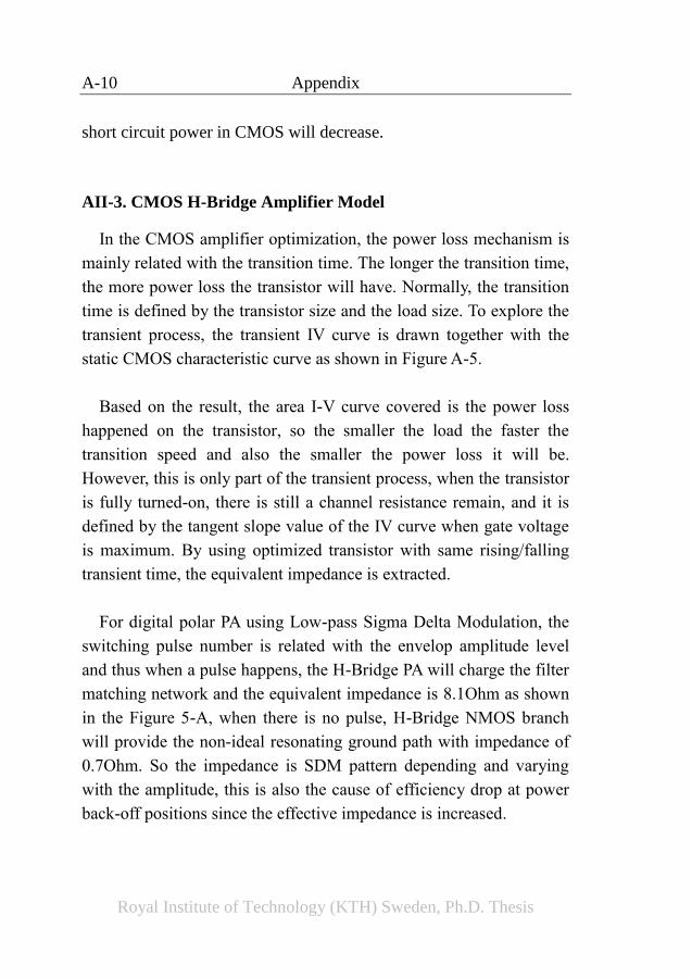
A-10 Appendix
Royal Institute of Technology (KTH) Sweden, Ph.D. Thesis
short circuit power in CMOS will decrease.
AII-3. CMOS H-Bridge Amplifier Model
In the CMOS amplifier optimization, the power loss mechanism is
mainly related with the transition time. The longer the transition time,
the more power loss the transistor will have. Normally, the transition
time is defined by the transistor size and the load size. To explore the
transient process, the transient IV curve is drawn together with the
static CMOS characteristic curve as shown in Figure A-5.
Based on the result, the area I-V curve covered is the power loss
happened on the transistor, so the smaller the load the faster the
transition speed and also the smaller the power loss it will be.
However, this is only part of the transient process, when the transistor
is fully turned-on, there is still a channel resistance remain, and it is
defined by the tangent slope value of the IV curve when gate voltage
is maximum. By using optimized transistor with same rising/falling
transient time, the equivalent impedance is extracted.
For digital polar PA using Low-pass Sigma Delta Modulation, the
switching pulse number is related with the envelop amplitude level
and thus when a pulse happens, the H-Bridge PA will charge the filter
matching network and the equivalent impedance is 8.1Ohm as shown
in the Figure 5-A, when there is no pulse, H-Bridge NMOS branch
will provide the non-ideal resonating ground path with impedance of
0.7Ohm. So the impedance is SDM pattern depending and varying
with the amplitude, this is also the cause of efficiency drop at power
back-off positions since the effective impedance is increased.
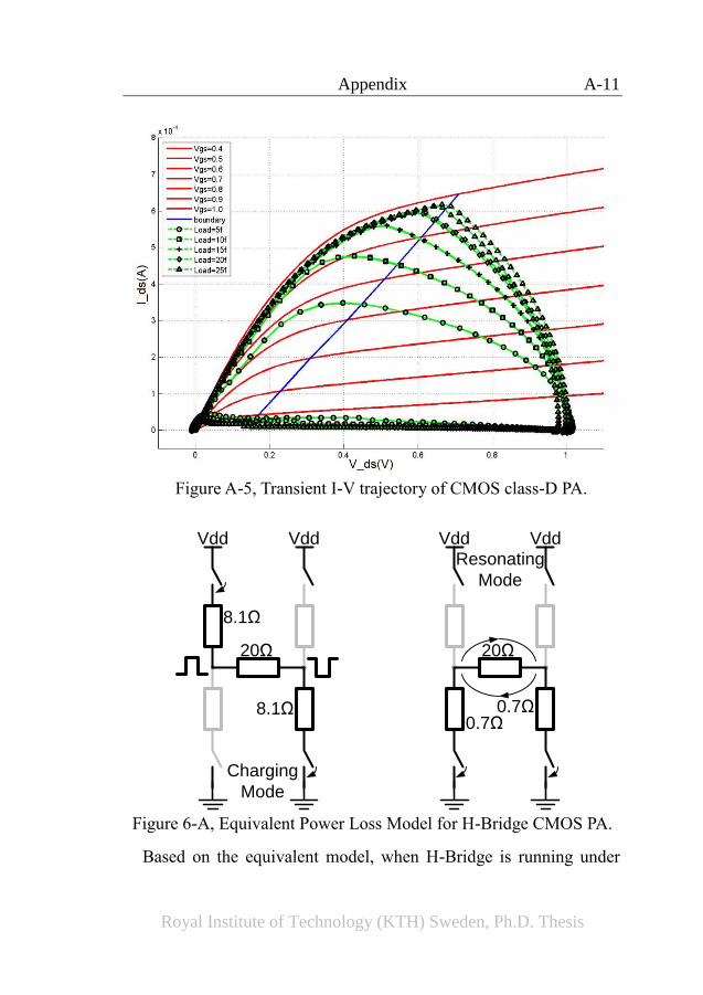
Appendix A-11
Royal Institute of Technology (KTH) Sweden, Ph.D. Thesis
Figure A-5, Transient I-V trajectory of CMOS class-D PA.
Vdd Vdd
8.1Ω
20Ω
8.1Ω
Vdd Vdd
0.7Ω
20Ω
0.7Ω
Charging
Mode
Resonating
Mode
Figure 6-A, Equivalent Power Loss Model for H-Bridge CMOS PA.
Based on the equivalent model, when H-Bridge is running under
A-12 Appendix
Royal Institute of Technology (KTH) Sweden, Ph.D. Thesis
full-swing envelop case, the maximum charging efficiency will be
2
2 2
2 / 2044.75%
2 / 20 2 / 8.1ch
V
V V
The result is complying with the circuit level optimization result of
38% as shown in the Figure 42. Other un-extracted parasitic is the
cause of the difference between these two values.
For a resonating case, assuming there is a perfect average
mechanism in the filter matching network and all the injected power
is averaged by pulses number. Then the filter matching network’s Q
factor must be taken into consideration because the ratio of emitted
power to the stored power in the resonating system will be defined by
the Q value. A simple model is built upon the power storage, waste
and emission as described in the main content of the thesis. If a pulse
is generated every cycle (full swing case), the highest efficiency’s
boundary is the charging efficiency ch . When the system is in the
non-full-swing case, the efficiency will drop since more power is
wasted on the grounding impedance. For example, when the system is
of 50% full-swing, there will be one changing period and one
resonating period with power ratio as listed below.
Activity Ground
Loss EM Storage Emission
Charging 0 1
ch
Q
Q
1ch
Q
Resonating 1
gnd ch
Q
Q
2
11 gnd ch
Q
Q
1 11 gnd ch
Q
Q Q
In this table, Q is the quality factor of filter matching network, gnd
is the resonating non-ideal ground power loss and it equals to 6.54%.

Appendix A-13
Royal Institute of Technology (KTH) Sweden, Ph.D. Thesis
Based on this trend, the total power loss equation for pulse pattern
100…0 can be calculated as follows, n is the zero pulse number.
1 1 1 /11
1 1 1 /
n
gnd
loss ch ch gnd
gnd
Q QQP
Q Q Q
Eq. (o)
Assuming Q=7, if the envelop level is 50% of full swing, n=1, the
normalized power loss ratio will be 57.8%, which in the stable
average case equals to 42.2% output efficiency. If the resonating
cycle number is 2, which equals to 1/3 of the full swing, the
efficiency will drop to 40.2%. And for n=3, efficiency is 38.6%. For
n=9, efficiency will be 33.9%. But in general trend, the curve is a
straight line as shown in the Figure 56.
This model reveal the resonating H-Bridge feature that the higher
the Q value, the higher the loss it will have for large power back-off
positions since more power stored will be wasted on the grounding
parasitic impedance. This is complying with the expectation of co-
design of the filter matching network with PA and the way to improve
efficiency will be increase the charging efficiency and reducing the
grounding parasitic loss.
In the model simulation, the real charging power loss will be even
higher and the cause of it is related with the non-ideal un-symmetrical
power supply network layout. This can be further improved with
balanced layout structure. The result of this model also revealed the
feature of pattern related parasitic impedance in the H-Bridge
amplifier and it is also important to know the filter matching network
will amplify the power loss effect and a suitable Q around 10 will be
enough to achieve balance efficiency performance.

Royal Institute of Technology (KTH) Sweden, Ph.D. Thesis
Bibliography
System Parameters and Developing Trend
[1]. Tim Haynes; , “Designing energy-smart 3G base stations”,
(http://rfdesign.com/mag/708RFDF1.pdf)
[2]. Kavousian, A.; Su, D.K.; Hekmat, M.; Shirvani, A.; Wooley, B.A.; , "A
Digitally Modulated Polar CMOS Power Amplifier With a 20-MHz
Channel Bandwidth," Solid-State Circuits, IEEE Journal of , vol.43,
no.10, pp.2251-2258, Oct. 2008.
[3]. Dinur, N.; Wulich, D.; , "Peak-to-average power ratio in high-order
OFDM," Communications, IEEE Transactions on , vol.49, no.6,
pp.1063-1072, Jun 2001
[4]. Biao Yan; Juan Yang; Hui Zhang; Yihuan Zhu; Haiyang Wang; ,
"Distribution Bound of PAPR in OFDM Signals," Communications,
Circuits and Systems Proceedings, 2006 International Conference on ,
vol.2, no., pp.1398-1401, 25-28 June 2006
[5]. Montes, L.A.; Suarez Penaloza, M.L.; Baudoin, G.; Villegas, M.; ,
"Specification of a polar sigma delta architecture for mobile multi-
radio transmitter - validation on IEEE 802.16e," Radio and Wireless
Symposium, 2008 IEEE , vol., no., pp.159-162, 22-24 Jan. 2008
[6]. Debaillie, B.; Bougard, B.; Lenoir, G.; Vandersteen, G.; Catthoor, F.; ,
"Energy-scalable OFDM transmitter design and control," Design
Automation Conference, 2006 43rd ACM/IEEE , vol., no., pp.536-541
[7]. Chin-Liang Wang; Yuan Ouyang; Hsien-Chih Chen; , "A peak-to-
average power ratio reduction technique for the IEEE 802.11a wireless
LAN," Vehicular Technology Conference, 2003. VTC 2003-Fall. 2003
IEEE 58th , vol.4, no., pp. 2287- 2291 Vol.4, 6-9 Oct. 2003
[8]. Tellambura, C.; Jayalath, A.D.S.; , "PAR reduction of an OFDM signal
using partial transmit sequences," Vehicular Technology Conference,
2001. VTC 2001 Fall. IEEE VTS 54th , vol.1, pp. 465- 469 vol.1, 2001
[9]. Kou, Y.J.; Lu, W.-S.; Antoniou, A.; , "A New Peak-to-Average Power-
Ratio Reduction Algorithm for OFDM Systems via Constellation
Extension," Wireless Communications, IEEE Transactions on , vol.6,
no.5, pp.1823-1832, May 2007
[10]. Garg V.K. ,; "An Overview of Wireless Systems"
http://media.techtarget.com/searchNetworkingChannel/downloads/08_
P375077_Ch03.pdf
[11]. Agilent WiMAX Concepts and RF Measurements Application Notes
(http://cp.literature.agilent.com/litweb/pdf/5989-2027EN.pdf)
[12]. Anritsu ACPR Measurement Application Notes
B-2 Bibliography
Royal Institute of Technology (KTH) Sweden, Ph.D. Thesis
(http://downloadfile.anritsu.com/RefFiles/en-US/Services-
Support/Downloads/Application-Notes/Application-Note/11410-
00264.pdf)
[13]. Analog Device Circuit Note CN-0134.
http://www.analog.com/static/imported-files/circuit_notes/CN0134.pdf
[14]. Jesse E. Chen, "Modeling RF Systems" (http://www.designers-
guide.org/Modeling/modeling-rf-systems.pdf)
[15]. Alim, O.A.; Elboghdadly, N.; Ashour, M.M.; Elaskary, A.M.; ,
"Simulation of channel estimation and equalization for WiMAX PHY
layer in simulink," Computer Engineering & Systems, 2007. ICCES
'07. International Conference on , pp.274-279, 27-29 Nov. 2007
[16]. Jie He; Jun Seok Yang; Yongsup Kim; Kim, A.S.; , "System-Level
Time-Domain Behavioral Modeling for A Mobile WiMax Transceiver,"
Behavioral Modeling and Simulation Workshop, Proceedings of the
2006 IEEE International , vol., no., pp.138-143, 14-15 Sept. 2006
[17]. May, T.; Rohling, H.; , "Reducing the peak-to-average power ratio in
OFDM radio transmission systems," Vehicular Technology Conference,
1998. VTC 98. 48th IEEE , vol.3, pp.2474-2478 vol.3, 18-21 May 1998
[18]. Sgrignoli, G.; , "Measuring peak/average power ratio of the
Zenith/AT&T DSC-HDTV signal with a vector signal analyzer,"
Broadcasting, IEEE Transactions on, vol.39,no.2,pp.255-264, Jun 1993
[19]. Jim Zyren (Freescale);, "Overview of the 3GPP Long Term Evolution
Physical Layer",
(http://www.freescale.com/files/wireless_comm/doc/white_paper/3GPP
EVOLUTIONWP.pdf)
[20]. Cecile Masse; , "A direct-conversion transmitter for WiMAX and
WiBro applications" (http://rfdesign.com/mag/601RFDF4.pdf)
[21]. Penaloza, M.; Baudoin, G.; Villegas, M.; , "A Cartesian Sigma-Delta
transmitter architecture," Radio and Wireless Symposium, 2009. RWS
'09. IEEE , vol., no., pp.51-54, 18-22 Jan. 2009
[22]. Jinsung Choi; Dongsu Kim; Daehyun Kang; Myoungsu Jun; Boshi Jin;
Jungmin Park; Bumman Kim; , "A 45/46/34% PAE linear polar
transmitter for EDGE/WCDMA/Mobile-WiMax," Microwave
Symposium Digest, 2009. MTT '09. IEEE MTT-S International , vol.,
no., pp.413-416, 7-12 June 2009
Software Defined Radio and ADC Receiver
Bibliography B-3
Royal Institute of Technology (KTH) Sweden, Ph.D. Thesis
[23]. Abidi, A.A.; , "The Path to the Software-Defined Radio Receiver,"
Solid-State Circuits, IEEE Journal of , vol.42,no.5, pp.954, May 2007
[24]. Giannini, V.; Nuzzo, P.; Soens, C.; Vengattaramane, K.; Steyaert, M.;
Ryckaert, J.; Goffioul, M.; Debaillie, B.; Van Driessche, J.; Craninckx,
J.; Ingels, M.; , "A 2mm2 0.1-to-5GHz SDR receiver in 45nm digital
CMOS," Solid-State Circuits Conference - Digest of Technical Papers,
2009. ISSCC 2009. IEEE International , pp.408-409, 8-12 Feb. 2009
[25]. Software Defined Radio – Wiki
(http://en.wikipedia.org/wiki/Software-defined_radio)
[26]. R. Langwieser; M. Fischer; A. L. Scholtz; M. Rupp; G. Humer,;
"Flexible Radio Frequency Hardware for a Software Definable Channel
Emulator"; (http://publik.tuwien.ac.at/files/pub-et_11363.pdf)
[27]. Liang Rong; Martin, E.; Gustafsson, I.; Rusu, A.; Ismail, M.; ,
"Systematic Design of a Flash ADC for UWB Applications," Quality
Electronic Design, 2007. ISQED '07. 8th International Symposium on ,
pp.108-114, 26-28 March 2007
[28]. Gustafsson, E. Martin I. "Reconfigurable Analog to Digital Converters
for Low Power Wireless Applications"
http://urn.kb.se/resolve?urn=urn:nbn:se:kth:diva-4774
Power Amplifiers
[29]. K. Mekechuk; W.J. Kim; etc;, "Linearizing Power Amplifiers Using
Digital Predistortion, EDA Tools and Test Hardware"
(http://cp.literature.agilent.com/litweb/pdf/5989-9030EN.pdf)
[30]. Poon; Alan Siu Kei , ECE 1352F Analog Integrated Circuits I Reading
Assignment - RF Power Amplifiers
(http://www.eecg.toronto.edu/~kphang/papers/2001/poon_RFamps.pdf)
[31]. Fritzin, J.; Johansson, T.; Alvandpour, A.; , "A 72.2Mbit/S LC-based
power amplifier in 65nm CMOS for 2.4Ghz 802.11n WLAN," Mixed
Design of Integrated Circuits and Systems, 2008. MIXDES 2008. 15th
International Conference on , vol., no., pp.155-158, 19-21 June 2008
[32]. Gustav Östberg; "A Comparative Study of Efficient Power Amplifiers
in CMOS" (http://liu.diva-
portal.org/smash/get/diva2:209021/FULLTEXT01)
[33]. Stauth, J.T.; Sanders, S.R.;,"A 2.4GHz, 20dBm class-D PA with single-
bit digital polar modulation in 90nm CMOS," Custom Integrated
Circuits Conference, 2008. CICC IEEE , pp.737-740, 21-24 Sept. 2008
B-4 Bibliography
Royal Institute of Technology (KTH) Sweden, Ph.D. Thesis
[34]. Cijvat, E.; Sjoland, H.; , "Two 130nm CMOS class-D RF power
amplifiers suitable for polar transmitter architectures," Solid-State and
Integrated-Circuit Technology, 2008. ICSICT 2008. 9th International
Conference on , vol., no., pp.1380-1383, 20-23 Oct. 2008
[35]. Mathews and Jeffs (Rane Corporation);, "Commercializing Class D
Amplifier Technologies";
http://www.rane.com/pdf/ranenotes/Class_D_Amplifier_Technologies.pdf
[36]. Piessens, T.; Steyaert, M.; , "Oscillator pulling and synchronisation
issues in self-oscillating class D power amplifiers," Solid-State Circuits
Conference, 2003. ESSCIRC '03. Proceedings of the 29th European ,
vol., no., pp.529-532, 16-18 Sept. 2003
[37]. Sekiya, H.; Sagawa, N.; Kazimierczuk, M.K.; , "Analysis of Class-DE
Amplifier With Linear and Nonlinear Shunt Capacitances at 25% Duty
Ratio," Circuits and Systems I: Regular Papers, IEEE Transactions on ,
vol.57, no.9, pp.2334-2342, Sept. 2010
[38]. Calvillo-Cortes, D.A.; Acar, M.; van der Heijden, M.P.; Apostolidou,
M.; de Vreede, L.C.N.; Leenaerts, D.; Sonsky, J.; , "A 65nm CMOS
pulse-width-controlled driver with 8Vpp output voltage for switch-
mode RF PAs up to 3.6GHz," Solid-State Circuits Conference Digest of
Technical Papers (ISSCC), 2011 IEEE International , vol., no., pp.58-
60, 20-24 Feb. 2011
[39]. Wagh, P.; Hidya, P.; , "High-efficiency switched-mode RF power
amplifier," Circuits and Systems, 2000. 42nd Midwest Symposium on ,
vol.2, no., pp.1044-1047 vol. 2, 1999
LINC/MLINC
[40]. Chireix, H.; , "High Power Outphasing Modulation," Proceedings of
the Institute of Radio Engineers , vol.23, no.11, pp. 1370, Nov. 1935
[41]. Cox, D.; , "Linear Amplification with Nonlinear Components,"
Communications, IEEE Transactions on , vol.22, no.12, pp. 1942-
1945, Dec 1974
[42]. Raab, F.; , "Efficiency of Outphasing RF Power-Amplifier Systems,"
Communications, IEEE Transactions on , vol.33, no.10, pp. 1094-
1099, Oct 1985
[43]. El-Asmar, M.; Birafane, A.; Kouki, A.; , "A Simplified Model for
Chireix Outphasing Combiner Efficiency," Microwave Conference,
2006. 36th European , vol., no., pp.192-195, 10-15 Sept. 2006
[44]. El-Amsar, M.; Birafane, A.; Kouki, A.B.; , "Optimization of the LINC
average power efficiency using Chireix combining systems," Industrial
Electronics, 2006 IEEE International Symposium on , vol.4, no.,
pp.3169-3172, 9-13 July 2006
Bibliography B-5
Royal Institute of Technology (KTH) Sweden, Ph.D. Thesis
[45]. Birafane, A.; Kouki, A.; , "An analytical approach to LINC power
combining efficiency estimation and optimization," Microwave
Conference, 2003. 33rd European , vol.3, pp. 1227Vol.3, 7-9 Oct. 2003
[46]. Casadevall, F.; Olmos, J.J.; , "On the behavior of the LINC
transmitter," Vehicular Technology Conference, 1990 IEEE 40th , vol.,
no., pp.29-34, 6-9 May 1990
[47]. Casadevall, F.J.; Valdovinos, A.; , "Performance analysis of QAM
modulations applied to the LINC transmitter," Vehicular Technology,
IEEE Transactions on , vol.42, no.4, pp.399-406, Nov 1993
[48]. Dinis, R.; Gusmao, A.; , "Signal processing schemes for
power/bandwidth efficient OFDM transmission with conventional or
LINC transmitter structures," Communications, 2001. ICC 2001. IEEE
International Conference on , vol.4, no., pp.1021-1027 vol.4, 2001
[49]. Hamedi-Hagh, S.; Salama, C.A.T.; , "Wideband CMOS integrated RF
combiner for LINC transmitters," Radio Frequency Integrated Circuits
(RFIC) Symposium, 2003 IEEE , pp. 555- 558, 8-10 June 2003
[50]. Hegazi, G.M.; Chu, T.T.; Groshong, R.A.; , "Improved LINC power
transmission using a quadrature outphasing technique," Microwave
Symposium Digest, 2005 IEEE MTT-S International , vol., no., pp. 4
pp., 12-17 June 2005
[51]. Helaoui, M.; Boumaiza, S.; Ghazel, A.; Ghannouchi, F.M.; , "Digital
compensation of branches imbalance effects in LINC transmitters,"
Microelectronics, 2004. ICM 2004 Proceedings. The 16th International
Conference on , vol., no., pp. 688- 691, 6-8 Dec. 2004
[52]. Kai-Yuan Jheng; Yi-Chiuan Wang; An-Yeu Wu; Hen-Wai Tsao; , "DSP
engine design for LINC wireless transmitter systems," Circuits and
Systems, 2006. ISCAS 2006. Proceedings. 2006 IEEE International
Symposium on , vol., no., pp.4 pp.-2596, 21-24 May 2006
[53]. Olson, S.A.; Stengel, R.E.; , "LINC imbalance correction using
baseband preconditioning," Radio and Wireless Conference, 1999.
RAWCON 99. 1999 IEEE , vol., no., pp.179-182, 1999
[54]. Sundstrom, L.; , "Spectral sensitivity of LINC transmitters to
quadrature modulator misalignments," Vehicular Technology, IEEE
Transactions on , vol.49, no.4, pp.1474-1487, Jul 2000
[55]. Birafane, A.; Kouki, A.B.; , "On the linearity and efficiency of
outphasing microwave amplifiers," Microwave Theory and Techniques,
IEEE Transactions on , vol.52, no.7, pp. 1702- 1708, July 2004
[56]. Birafane, A.; Kouki, A.B.; , "Phase-only predistortion for LINC
amplifiers with Chireix-outphasing combiners," Microwave Theory and
Techniques,IEEE Transactions on,vol53,no.6, pp.2240-2250,June 2005
[57]. Strandberg, R.; Andreani, P.; Sundstrom, L.; , "Spectrum emission
B-6 Bibliography
Royal Institute of Technology (KTH) Sweden, Ph.D. Thesis
considerations for baseband-modeled CALLUM architectures,"
Microwave Theory and Techniques, IEEE Transactions on , vol.53,
no.2, pp.660-669, Feb. 2005
[58]. Gang Liu; Haldi, P.; Tsu-Jae King Liu; Niknejad, A.M.; , "Fully
Integrated CMOS Power Amplifier With Efficiency Enhancement at
Power Back-Off," Solid-State Circuits, IEEE Journal of , vol.43, no.3,
pp.600-609, March 2008
[59]. Jennings, D.J.; McGeehan, J.P.; , "A high-efficiency RF transmitter
using VCO-derived synthesis: CALLUM," Radio and Wireless
Conference, 1998. RAWCON 98. 1998 IEEE , vol., no., pp.137-140, 9-
12 Aug 1998
[60]. Helaoui, M.; Boumaiza, S.; Ghannouchi, F. M.; Kouki, A. B.; Ghazel,
A.; , "A New Mode-Multiplexing LINC Architecture to Boost the
Efficiency of WiMAX Up-Link Transmitters," Microwave Theory and
Techniques, IEEE Transactions on , vol.55, no.2, pp.248, Feb. 2007
[61]. Choffrut, A.; Van Veen, B.D.; Booske, J.H.; , "Minimizing Spectral
Leakage of Nonideal LINC Transmitters by Analysis of Component
Impairments," Vehicular Technology, IEEE Transactions on , vol.56,
no.2, pp.445-458, March 2007
[62]. Helaoui, M.; Boumaiza, S.; Ghannouchi, F.M.; , "On the dynamic
range improvement and robustness against branch imbalance of mode-
multiplexing LINC amplifiers," Microwave Conference, 2007.
European, vol., no., pp.178-181, 9-12 Oct. 2007
[63]. Conradi, C.P.; McRory, J.G.; , "Predistorted LINC transmitter,"
Electronics Letters , vol.38, no.7, pp.301-302, 28 Mar 2002
[64]. Zhang, X.; Larson, L.E.; Asbeck, P.M.; Nanawa, P.; , "Gain/phase
imbalance-minimization techniques for LINC transmitters ,"
Microwave Theory and Techniques, IEEE Transactions on , vol.49,
no.12, pp.2507-2516, Dec 2001
[65]. Xuejun Zhang; Larson, L.E.; Asbeck, P.M.; Langridge, R.A.; ,
"Analysis of power recycling techniques for RF and microwave
outphasing power amplifiers," Circuits and Systems II: Analog and
Digital Signal Processing, IEEE Transactions on , vol.49, no.5, pp.
312- 320, May 2002
[66]. Stengel, B.; Eisenstadt, W.R.; , "LINC power amplifier combiner
method efficiency optimization," Vehicular Technology, IEEE
Transactions on , vol.49, no.1, pp.229-234, Jan 2000
[67]. Yuan-Chuan Chen; Kai-Yuan Jheng; An-Yeu Wu; Hen-Wai Tsao;
Bosen Tzeng; , "Multilevel LINC System Design for Wireless
Transmitters," VLSI Design, Automation and Test, 2007. VLSI-DAT
2007. International Symposium on , vol., no., pp.1-4, 25-27 April 2007
[68]. Poitau, G.; Kouki, A.; , "MILC: Modified Implementation of the LINC
Bibliography B-7
Royal Institute of Technology (KTH) Sweden, Ph.D. Thesis
Concept," Microwave Symposium Digest, 2006. IEEE MTT-S
International , vol., no., pp.1883-1886, 11-16 June 2006
Polar Transmitters
[69]. Groe, J.; , "Polar Transmitters for Wireless Communications,"
Communications Magazine, IEEE , vol.45, no.9, pp.58-63, Sept. 2007
[70]. Huang, Yonghui; Mikkelsen, Jan Hvolgaard; Larsen, Torben; ,
"Investigation of Polar Transmitters for WCDMA Handset
Applications," Norchip Conference, 2006. 24th, pp.155-158, Nov. 2006
[71]. Jinseong Jeong; Wang, Y.E.; , "A Polar Delta-Sigma Modulation
(PDSM) Scheme for High Efficiency Wireless Transmitters,"
Microwave Symposium, 2007. IEEE/MTT-S International , vol., no.,
pp.73-76, 3-8 June 2007
[72]. Kenney, J.S.; , "Behavioral modeling for polar transmitters," Wireless
and Microwave Technology Conference, 2009. WAMICON '09. IEEE
10th Annual , vol., no., pp.1-4, 20-21 April 2009
[73]. Deuk Lee; Senguttuvan, R.; Chatterjee, A.; , "Efficient testing of
wireless polar transmitters," Mixed-Signals, Sensors, and Systems Test
Workshop, 2008. IMS3TW 2008. IEEE 14th International , vol., no.,
pp.1-5, 18-20 June 2008
[74]. Loke, W.-F.; Chia, M.Y.-W.; Chee, P.-Y.; , "Design considerations for
multi-band OFDM polar transmitter of UWB system," Electronics
Letters , vol.43, no.22, Oct. 25 2007
[75]. McCune, E.W., Jr.; , "Multi-mode and multi-band polar transmitter for
GSM, NADC, and EDGE," Wireless Communications and Networking,
2003. WCNC 2003. 2003 IEEE , vol.2, pp.812vol.2, 20-20 March 2003
[76]. Priyanto, B.E.; Sorensen, T.B.; Jensen, O.K.; Larsen, T.; Kolding, T.;
Mogensen, P.; , "Impact of polar transmitter imperfections on UTRA
LTE uplink performance," Norchip, 2007 , pp.1-4, 19-20 Nov. 2007
[77]. K.-H. Seah; M.Y.-W. Chia; C. Papavassiliou; G.A. Constantinides; ,
"Digital polar transmitter for ultra-wideband system using OFDM
modulation," Electronics Letters , vol.43, no.8, pp.466, April 12 2007
[78]. Strasser, G.; Lindner, B.; Maurer, L.; Hueber, G.; Springer, A.; , "On
the Spectral Regrowth in Polar Transmitters," Microwave Symposium
Digest, 2006. IEEE MTT-S International , pp.781, 11-16 June 2006
[79]. Talonen, M.; Lindfors, S.; , "System requirements for OFDM polar
transmitter," Circuit Theory and Design, 2005. Proceedings of the 2005
European Conference on , vol.3, no., pp. III/69- III/72 vol. 3, 28 Aug.-2
Sept. 2005
B-8 Bibliography
Royal Institute of Technology (KTH) Sweden, Ph.D. Thesis
[80]. Jinghua Zhang; Bo Shi; Yong Lian; , "Performance evaluation on polar
transmitters using delta and delta-sigma modulations," Information,
Communications & Signal Processing, 2007 6th International
Conference on , vol., no., pp.1-4, 10-13 Dec. 2007
[81]. Jianyi Zhou; Jianhong Chen; Jianing Zhao; Jianjun Wang; Wei Kang; ,
"Design of a high performance RF transceiver for WiMax basestation,"
Microwave Conference Proceedings, 2005. APMC 2005. Asia-Pacific
Conference Proceedings , vol.5, no., pp. 4 pp., 4-7 Dec. 2005
[82]. Kousai, S.; Miyashita, D.; Wadatsumi, J.; Maki, A.; Sekiguchi, T.; Ito,
R.; Hamada, M.; , "A 1.2V 0.2-to-6.3GHz Transceiver with Less Than -
29.5dB EVM@-3dBm and a Choke/Coil-Less Pre-Power Amplifier,"
Solid-State Circuits Conference, 2008. ISSCC 2008. Digest of
Technical Papers. IEEE International , pp.214-608, 3-7 Feb. 2008
[83]. Tobias Andersson; Johan Wahlsten;, "Sigma Delta modulation Applied
to Switching RF Power Amplifiers", (http://liu.diva-
portal.org/smash/get/diva2:23917/FULLTEXT01)
[84]. Ulf Gustavsson;, "Design of an inverse class D amplifier using GaN
HEMT technology"; (http://www.oru.se/PageFiles/14896/Exa037-
mag102_06.pdf)
[85]. Wangmyong Woo; Kyu Hwan An; Lee, O.; Jae Joon Chang; Chang-Ho
Lee; Kiseok Yang; Mi Jeong Park; Haksun Kim; Laskar, J.; , "A novel
linear polar transmitter architecture using low-power analog
predistortion for EDGE applications," Microwave Conference, 2006.
APMC 2006. Asia-Pacific , vol., no., pp.1102-1105, 12-15 Dec. 2006
[86]. Berland, C.; Hibon, I.; Bercher, J.F.; Villegas, M.; Belot, D.; Pache, D.;
Le Goascoz, V.; , "A transmitter architecture for nonconstant envelope
modulation," Circuits and Systems II: Express Briefs, IEEE
Transactions on , vol.53, no.1, pp.13-17, Jan. 2006
[87]. Chung-Chun Chen; Hung-Yang Ko; Yi-Chiuan Wang; Hen-Wai Tsao;
Kai-Yuan Jheng; An-Yeu Wu; , "Polar transmitter for wireless
communication system," Intelligent Signal Processing and
Communication Systems, 2005. ISPACS 2005. Proceedings of 2005
International Symposium on , vol., no., pp. 613- 616, 13-16 Dec. 2005
[88]. van Zeijl, P.T.M.; Collados, M.; , "A Digital Envelope Modulator for
an OFDM WLAN Polar Transmitter in 90 nm CMOS," VLSI Design,
Automation and Test, 2007. VLSI-DAT 2007. International Symposium
on , vol., no., pp.1-4, 25-27 April 2007
[89]. Wagh, P.; Midya, P.; Rakers, P.; Caldwell, J.; Schooler, T.; , "An all-
digital universal RF transmitter [CMOS RF modulator and PA],"
Custom Integrated Circuits Conference, 2004. Proceedings of the IEEE
2004 , vol., no., pp. 549- 552, 3-6 Oct. 2004
Bibliography B-9
Royal Institute of Technology (KTH) Sweden, Ph.D. Thesis
EER
[90]. Feipeng Wang; Kimball, D.F.; Popp, J.D.; Yang, A.H.; Lie, D.Y.;
Asbeck, P.M.; Larson, L.E.; , "An Improved Power-Added Efficiency
19-dBm Hybrid Envelope Elimination and Restoration Power
Amplifier for 802.11g WLAN Applications," Microwave Theory and
Techniques, IEEE Transactions on , vol.54, no.12, pp.4086, Dec. 2006
[91]. Wang, F.; Kimball, D.; Popp, J.; Yang, A.; Lie, D.Y.C.; Asbeck, P.;
Larson, L.; , "Wideband envelope elimination and restoration power
amplifier with high efficiency wideband envelope amplifier for WLAN
802.11g applications," Microwave Symposium Digest, 2005 IEEE
MTT-S International , vol., no., pp. 4 pp., 12-17 June 2005
Polar (Power Modulator)
[92]. Renliang Zheng; Mihai Sanduleanu; Aditham, R.P.; de Vreede, L.C.N.;
Junyan Ren; , "A 5.5-GHz Power Amplifier For Wide Bandwidth Polar
Modulator," Solid-State and Integrated Circuit Technology, 2006.
ICSICT '06. 8th International Conference on , vol., no., pp.1724-1726,
23-26 Oct. 2006
[93]. Tae-Woo Kwak; Min-Chul Lee; Gyu-Hyeong Cho; , "A 2 W CMOS
Hybrid Switching Amplitude Modulator for EDGE Polar Transmitters,"
Solid-State Circuits, IEEE Journal of , vol.42, no.12, pp.2666-2676,
Dec. 2007
[94]. Shrestha, R.; van der Zee, R.; de Graauw, A.; Nauta, B.; , "A Wideband
Supply Modulator for 20 MHz RF Bandwidth Polar PAs in 65 nm
CMOS," Solid-State Circuits, IEEE Journal of , vol.44, no.4, pp.1272-
1280, April 2009
[95]. van Zeijl, P.T.M.; Collados, M.; , "A Digital Envelope Modulator for a
WLAN OFDM Polar Transmitter in 90 nm CMOS," Solid-State
Circuits, IEEE Journal of , vol.42, no.10, pp.2204-2211, Oct. 2007
[96]. Woo-Young Kim; Ki-Young Kim; Seung-Tak Ryu; Jae-Kil Jung; Chul
Soon Park; , "1-bit and multi-bit envelope delta-sigma modulators for
CDMA polar transmitters," Microwave Conference, 2008. APMC 2008.
Asia-Pacific , vol., no., pp.1-4, 16-20 Dec. 2008
[97]. Kitchen, J.N.; Chu, C.; Kiaei, S.; Bakkaloglu, B.; , "Combined Linear
and -Modulated Switch-Mode PA Supply Modulator for Polar
Transmitters," Solid-State Circuits, IEEE Journal of , vol.44, no.2,
pp.404-413, Feb. 2009
[98]. Kitchen, J.; Connie Chu; Kiaei, S.; Bakkaloglu, B.; , "Supply
modulators for RF polar transmitters," Radio Frequency Integrated
B-10 Bibliography
Royal Institute of Technology (KTH) Sweden, Ph.D. Thesis
Circuits Symposium, 2008. RFIC 2008. IEEE , vol., no., pp.417-420,
June 17 2008-April 17 2008
[99]. Yan, S.; Sanchez-Sinencio, E.; , "A continuous-time sigma-delta
modulator with 88-dB dynamic range and 1.1-MHz signal bandwidth,"
Solid-State Circuits, IEEE Journal of , vol.39, no.1, pp. 75, Jan. 2004
[100]. Collados, M.; van Zeijl, P.T.M.; Pavlovic, N.; , "High-power digital
envelope modulator for a polar transmitter in 65nm CMOS," Custom
Integrated Circuits Conference, 2008. CICC 2008. IEEE , vol., no.,
pp.733-736, 21-24 Sept. 2008
[101]. Nisbet, J.; , "Polar modulators for 1 and 2 GHz power amplifier
correction," Bipolar/BiCMOS Circuits and Technology Meeting,
Proceedings of the 2001 , vol., no., pp.94-97, 2001
[102]. Nagle, P.; Burton, P.; Heaney, E.; McGrath, F.; , "A wide-band linear
amplitude modulator for polar transmitters based on the concept of
interleaving delta modulation," Solid-State Circuits, IEEE Journal of ,
vol.37, no.12, pp. 1748- 1756, Dec 2002
[103]. Nielsen, M.; Larsen, T.; , "A 2-GHz GaAs HBT RF Pulsewidth
Modulator," Microwave Theory and Techniques, IEEE Transactions
on , vol.56, no.2, pp.300-304, Feb. 2008
Polar (Class-E/ Direct RF)
[104]. Staszewski, R.B.; Rezeq, S.; Chih-Ming Hung; Cruise, P.; Wallberg,
J.; , "Sigma-delta noise shaping for digital-to-frequency and digital-to-
RF-amplitude conversion," System-on-Chip for Real-Time
Applications, 2005. Proceedings. Fifth International Workshop on ,
vol., no., pp. 154- 159, 20-24 July 2005
[105]. Cabral, P.M.; Pedro, J.C.; Garcia, J.A.; Cabria, L.; , "A linearized
polar transmitter for wireless applications," Microwave Symposium
Digest, 2008 IEEE MTT-S International , pp.935-938, 15-20 June 2008
[106]. Jau-Horng Chen; Fedorenko, P.; Kenney, J.S.; , "A low voltage W-
CDMA polar transmitter with digital envelope path gain
compensation," Microwave and Wireless Components Letters, IEEE ,
vol.16, no.7, pp.428-430, July 2006
[107]. Fallesen, C.; Asbeck, P.; , "A 1 W 0.35 µm CMOS power amplifier
for GSM-1800 with 45% PAE," Solid-State Circuits Conference, 2001.
Digest of Technical Papers. ISSCC. 2001 IEEE International , vol., no.,
pp.158-159, 2001
[108]. Fritzin, J.; Alvandpour, A.; , "Low Voltage Class-E Power Amplifiers
for DECT and Bluetooth in 130nm CMOS," Silicon Monolithic
Integrated Circuits in RF Systems, 2009. SiRF '09. IEEE Topical
Meeting on , vol., no., pp.1-4, 19-21 Jan. 2009
Bibliography B-11
Royal Institute of Technology (KTH) Sweden, Ph.D. Thesis
[109]. Hietakangas, S.; Rautio, T.; Rahkonen, T.; , "1 GHz Class E RF
Power Amplifier For A Polar Transmitter," Norchip Conference, 2006.
24th , vol., no., pp.5-9, Nov. 2006
[110]. Younsuk Kim; Bon-Hyun Ku; Changkun Park; Dong Ho Lee;
Songcheol Hong; , "A High Dynamic Range CMOS RF Power
Amplifier with a Switchable Transformer for Polar Transmitters,"
Radio Frequency Integrated Circuits (RFIC) Symposium, 2007 IEEE ,
vol., no., pp.737-740, 3-5 June 2007
[111]. Kitchen, J.D.; Deligoz, I.; Kiaei, S.; Bakkaloglu, B.; , "Linear RF
polar modulated SiGe Class E and F power amplifiers," Radio
Frequency Integrated Circuits (RFIC) Symposium, 2006 IEEE , vol.,
no., pp.4 pp., 11-13 June 2006
[112]. Kunihiro, K.; Takahashi, K.; Yamanouchi, S.; Hirayama, T.; Hida, H.;
Tanaka, S.; , "A Polar Transmitter Using a Linear-Assisted Delta-
Modulation Envelope-Amplifier for WCDMA Applications,"
Microwave Conference, 2006. 36th European , vol., no., pp.137-140,
10-15 Sept. 2006
[113]. Lopez, N.D.; Xufeng Jiang; Maksimovic, D.; Popovic, Z.; , "Class-E
Power Amplifier in a Polar EDGE Transmitter," Microwave Symposium
Digest, 2006. IEEE MTT-S International , vol., no., pp.785-788, 11-16
June 2006
[114]. Lopez, N.D.; Xufeng Jiang; Maksimovic, D.; Popovic, Z.; , "A high-
efficiency linear polar transmitter for EDGE," Radio and Wireless
Symposium, 2008 IEEE , vol., no., pp.199-202, 22-24 Jan. 2008
[115]. Shameli, A.; Safarian, A.; Rofougaran, A.; Rofougaran, M.; de
Flaviis, F.; , "A Novel DAC Based Switching Power Amplifier for
Polar Transmitter," Custom Integrated Circuits Conference, 2006.
CICC '06. IEEE , vol., no., pp.137-140, 10-13 Sept. 2006
[116]. Narisi Wang; Xinli Peng; Yousefzadeh, V.; Maksimovic, D.; Pajic, S.;
Popovic, Z.; , "Linearity of X-band class-E power amplifiers in EER
operation," Microwave Theory and Techniques, IEEE Transactions on ,
vol.53, no.3, pp. 1096- 1102, March 2005
[117]. Jinsung Choi; Jounghyun Yim; Jinho Yang; Jingook Kim; Jeonghyun
Cha; Daehyun Kang; Dongsu Kim; Bumman Kim; , "A Sigma Delta-
Digitized Polar RF Transmitter," Microwave Theory and Techniques,
IEEE Transactions on , vol.55, no.12, pp.2679-2690, Dec. 2007
[118]. Jang, J.; Changkun Park; Haksun Kim; Hong, S.; , "A CMOS RF
Power Amplifier Using an Off-Chip Transmision Line Transformer
With 62% PAE," Microwave and Wireless Components Letters, IEEE ,
vol.17, no.5, pp.385-387, May 2007
[119]. Kavousian, A.; Su, D.K.; Wooley, B.A.; , "A Digitally Modulated
B-12 Bibliography
Royal Institute of Technology (KTH) Sweden, Ph.D. Thesis
Polar CMOS PA with 20MHz Signal BW," Solid-State Circuits
Conference, 2007. ISSCC 2007. Digest of Technical Papers. IEEE
International , vol., no., pp.78-588, 11-15 Feb. 2007
[120]. Kitchen, J. N.; Deligoz, I.; Kiaei, S.; Bakkaloglu, B.; , "Polar SiGe
Class E and F Amplifiers Using Switch-Mode Supply Modulation,"
Microwave Theory and Techniques, IEEE Transactions on , vol.55,
no.5, pp.845-856, May 2007
[121]. Park, C.; Kim, Y.; Kim, H.; Hong, S.; , "A 1.9-GHz Triple-Mode
Class-E Power Amplifier for a Polar Transmitter," Microwave and
Wireless Components Letters, IEEE , vol.17, no.2, pp.148, Feb. 2007
[122]. Pedro, J.C.; Garcia, J.A.; Cabral, P.M.; , "Nonlinear Distortion
Analysis of Polar Transmitters," Microwave Theory and Techniques,
IEEE Transactions on , vol.55, no.12, pp.2757-2765, Dec. 2007
[123]. Presti, C.D.; Carrara, F.; Scuderi, A.; Asbeck, P.M.; Palmisano, G.; ,
"A 25 dBm Digitally Modulated CMOS Power Amplifier for
WCDMA/EDGE/OFDM With Adaptive Digital Predistortion and
Efficient Power Control," Solid-State Circuits, IEEE Journal of ,
vol.44, no.7, pp.1883-1896, July 2009
[124]. Reynaert, P.; Steyaert, M.S.J.; , "A 1.75-GHz polar modulated CMOS
RF power amplifier for GSM-EDGE," Solid-State Circuits, IEEE
Journal of , vol.40, no.12, pp. 2598- 2608, Dec. 2005
[125]. Shameli, A.; Safarian, A.; Rofougaran, A.; Rofougaran, M.; De
Flaviis, F.; , "A Two-Point Modulation Technique for CMOS Power
Amplifier in Polar Transmitter Architecture," Microwave Theory and
Techniques, IEEE Transactions on , vol.56, no.1, pp.31-38, Jan. 2008
[126]. Ali M Niknejad;, "Class E/F Amplifiers",
http://rfic.eecs.berkeley.edu/~niknejad/ee242/pdf/eecs242_class_EF_P
As.pdf
[127]. McCune, E.; , "Polar modulation and bipolar RF power devices,"
Bipolar/BiCMOS Circuits and Technology Meeting, 2005. Proceedings
of the , vol., no., pp. 1- 5, 9-11 Oct. 2005
[128]. Shrestha, R.; Van der Zee, R.A.R.; de Graauw, A.J.M.; Nauta, B.; , "A
wideband supply modulator for 20MHz RF bandwidth polar PAs in
65nm CMOS," VLSI Circuits, 2008 IEEE Symposium on , vol., no.,
pp.92-93, 18-20 June 2008
[129]. van Zeijl, P.T.M.; Collados, M.; , "A Multi-Standard Digital Envelope
Modulator for Polar Transmitters in 90nm CMOS," Radio Frequency
Integrated Circuits (RFIC) Symposium, 2007 IEEE , pp.373 June 2007
[130]. Wing-Yee Chu; Bakkaloglu, B.; Kiaei, S.; , "A 10MHz-Bandwidth
2mV-Ripple PA-Supply Regulator for CDMA Transmitters," Solid-
State Circuits Conference, 2008. ISSCC 2008. Digest of Technical
Papers. IEEE International , vol., no., pp.448-626, 3-7 Feb. 2008

Bibliography B-13
Royal Institute of Technology (KTH) Sweden, Ph.D. Thesis
Polar (PWM)
[131]. Raab, F.; , "Radio Frequency Pulsewidth Modulation,"
Communications, IEEE Transactions on,vol.21,no.8,pp. 958, Aug 1973
[132]. Laflere, W.; Steyaert, M.; Craninckx, J.; , "A power amplifier driver
using self-oscillating pulse-width modulators," Solid State Circuits
Conference, 2007. ESSCIRC 2007. 33rd European , vol., no., pp.380-
383, 11-13 Sept. 2007
[133]. Nielsen, M.; Larsen, T.; , "An RF Pulse Width Modulator for Switch-
Mode Power Amplification of Varying Envelope Signals," Silicon
Monolithic Integrated Circuits in RF Systems, 2007 Topical Meeting
on , vol., no., pp.277-280, 10-12 Jan. 2007
Polar (BPDSM)
[134]. Johnson, T.; Sobot, R.; Stapleton, S.; , "Measurement of Bandpass
Sigma-Delta Modulator Coding Efficiency and Pulse Transition
Frequency for RF Class D Power Amplifier Applications," Electrical
and Computer Engineering, 2006. CCECE '06. Canadian Conference
on , vol., no., pp.2314-2317, 7-10 May 2006
[135]. Frappe, A.; Flament, A.; Stefanelli, B.; Kaiser, A.; Cathelin, A.; , "An
All-Digital RF Signal Generator Using High-Speed Modulators,"
Solid-State Circuits, IEEE Journal of , vol.44, no.10, pp.2722-2732,
Oct. 2009
[136]. Tsai-Pi Hung; Rode, J.; Larson, L.E.; Asbeck, P.M.; , "Design of H-
Bridge Class-D Power Amplifiers for Digital Pulse Modulation
Transmitters," Microwave Theory and Techniques, IEEE Transactions
on , vol.55, no.12, pp.2845-2855, Dec. 2007
[137]. Johnson, T.; Stapleton, S. P.; , "RF Class-D Amplification With
Bandpass Sigma–Delta Modulator Drive Signals," Circuits and
Systems I: Regular Papers, IEEE Transactions on , vol.53, no.12,
pp.2507-2520, Dec. 2006
Polar (LPSDM)
[138]. Hernandez, L.; Wiesbauer, A.; Paton, S.; Di Giandomencio, A.; ,
"Modelling and optimization of low pass continuous-time sigma delta
modulators for clock jitter noise reduction," Circuits and Systems,
2004. ISCAS '04. Proceedings of the 2004 International Symposium
on , vol.1, no., pp. I- 1072-5 Vol.1, 23-26 May 2004
B-14 Bibliography
Royal Institute of Technology (KTH) Sweden, Ph.D. Thesis
[139]. Nielsen, M.; Larsen, T.; , "A Transmitter Architecture Based on
Delta–Sigma Modulation and Switch-Mode Power Amplification,"
Circuits and Systems II: Express Briefs, IEEE Transactions on , vol.54,
no.8, pp.735-739, Aug. 2007
[140]. Suarez Penaloza, M.L.; Valenta, V.; Baudoin, G.; Villegas, M.; ,
"Study of a modified Polar Sigma-Delta transmitter architecture for
multi-radio applications," Wireless Technology, 2008. EuWiT 2008.
European Conference on , vol., no., pp.222-225, 27-28 Oct. 2008
Doherty
[141]. Doherty, W.H.; , "A New High Efficiency Power Amplifier for
Modulated Waves," Proceedings of the Institute of Radio Engineers ,
vol.24, no.9, pp. 1163- 1182, Sept. 1936
[142]. Sirois, J.; Boumaiza, S.; Helaoui, M.; Brassard, G.; Ghannouchi,
F.M.; , "A robust modeling and design approach for dynamically
loaded and digitally linearized Doherty amplifiers," Microwave Theory
and Techniques, IEEE Transactions on , vol.53, no.9, pp. 2875- 2883,
Sept. 2005
Coding Efficiency
[143]. Pornpromlikit, S.; Jinho Jeong; Presti, C.D.; Scuderi, A.; Asbeck,
P.M.; , "A 25-dBm high-efficiency digitally-modulated SOI CMOS
power amplifier for multi-standard RF polar transmitters," Radio
Frequency Integrated Circuits Symposium, 2009. RFIC 2009. IEEE ,
vol., no., pp.157-160, 7-9 June 2009
[144]. Johnson, T.; Stapleton, S.P.; , "Comparison of Bandpass Modulator
Coding Efficiency With a Periodic Signal Model," Circuits and
Systems I: Regular Papers, IEEE Transactions on , vol.55, no.11,
pp.3763-3775, Dec. 2008
Compensation Methods
[145]. Cavers, J.K.; , "Amplifier linearization using a digital predistorter
with fast adaptation and low memory requirements," Vehicular
Technology, IEEE Transactions on , vol.39, no.4, pp.374, Nov 1990
[146]. Gimlin, D.R.; Patisaul, C.R.; , "On minimizing the peak-to-average
Bibliography B-15
Royal Institute of Technology (KTH) Sweden, Ph.D. Thesis
power ratio for the sum of N sinusoids," Communications, IEEE
Transactions on , vol.41, no.4, pp.631-635, Apr 1993
[147]. Tarokh, V.; Jafarkhani, H.; , "On the computation and reduction of the
peak-to-average power ratio in multicarrier communications,"
Communications, IEEE Transactions on , vol.48, no.1, pp.37, Jan 2000
[148]. Cabria, L.; Garcia, J.A.; Cabral, P.M.; Pedro, J.C.; , "Linearization of
a polar transmitter for EDGE applications," Integrated Nonlinear
Microwave and Millimetre-Wave Circuits, 2008. INMMIC 2008.
Workshop on , vol., no., pp.115-118, 24-25 Nov. 2008
[149]. Devlin, C.; Anding Zhu; Kenney, J.S.; Brazil, T.J.; , "Peak reduction
technique for sigma delta modulator in the envelope path of polar
transmitter," Wireless Technology, 2008. EuWiT 2008. European
Conference on , vol., no., pp.206-209, 27-28 Oct. 2008
[150]. Hietakangas, S.; Rautio, T.; Rahkonen, T.; , "Feedthrough
cancellation in a class E amplified polar transmitter," Circuit Theory
and Design, 2007. ECCTD 2007. 18th European Conference on , vol.,
no., pp.591-594, 27-30 Aug. 2007
[151]. Philippe, P.; , "A zero crossing avoidance predistortion technique for
polar transmitters," Electronics, Circuits and Systems, 2008. ICECS
2008. 15th IEEE International Conference on , vol., no., pp.814-817,
Aug. 31 2008-Sept. 3 2008
[152]. Hyun Jin Yoo; Yun Seong Eo; , "A Highly Linear CMOS Power
Amplifier with AM-AM and AM-PM Compensation for 2.3GHz
Wibro/WiMax Applications," Microwave Conference, 2007. APMC
2007. Asia-Pacific , vol., no., pp.1-4, 11-14 Dec. 2007
SAFF
[153]. Nikolic, B.; Oklobdzija, V.G.; Stojanovic, V.; Wenyan Jia; James Kar-
Shing Chiu; Ming-Tak Leung, M.; , "Improved sense-amplifier-based
flip-flop: design and measurements," Solid-State Circuits, IEEE
Journal of , vol.35, no.6, pp.876-884, June 2000
Components Transistor Process
[154]. Suematsu, N.; , "On-chip matching Si-MMIC for mobile
communication terminal application," Radio Frequency Integrated
Circuits (RFIC) Symposium, 1997., IEEE , pp.9-12, 8-11 Jun 1997
B-16 Bibliography
Royal Institute of Technology (KTH) Sweden, Ph.D. Thesis
[155]. Sakurai, T.; Newton, A.R.; , "Alpha-power law MOSFET model and
its applications to CMOS inverter delay and other formulas," Solid-
State Circuits, IEEE Journal of , vol.25, no.2, pp.584-594, Apr 1990
[156]. Marante, R.; Garcia, J.A.; Cabral, P.M.; Pedro, J.C.; , "Impact of
Ron(VDD) dependence on polar transmitter residual distortion,"
Integrated Nonlinear Microwave and Millimetre-Wave Circuits, 2008.
INMMIC 2008. Workshop on , vol., no., pp.123-126, 24-25 Nov. 2008
Class D Power Amplifiers
[157]. Wolfson Electronics, "Class D Amplifiers Empower Mobile
Multimedia" ,(http://www.wolfsonmicro.com/documents/uploads/misc/
en/Class_D_Amplifiers_Empower_Mobile_Multimedia.pdf)
RFID Standards
[158]. EPC UHF Radio Frequency Identity Protocols: Class-1 Generation-2
UHF RFID Protocol for Communications at 860MHz-960MHz,
Version 1.2.0, 23rd Oct. 2008.
[159]. ISO/IEC 18000-6:2010(E): Parameters for air interface
communications at 860 MHz to 960 MHz. Second Edition. 2010.
[160]. Liang Rong; Lirong Zheng; , "A polar transmitter architecture with
digital switching amplifier for UHF RFID applications," RFID (RFID),
2011 IEEE International Conference on , pp.1-6, 12-14 April 2011
Books
[161]. David A. Johns, Ken Martin, “Analog Integrated Circuit Design”,
Wiley & Sons, Inc., 1997.
[162]. Jack R Smith, “Modern Communication Circuits”, McGraw-Hill
Science/Engineering/Math; 2 edition (August 1, 1997)
[163]. Xuejun Zhang; Lawrence E. Larson; Peter M. Asbeck;, “Design of
Linar RF Outphasing Power Amplifiers”, Artech House Microwave
Library, ISBN 1580533744, 9781580533744
[164]. Peter B. Kenington;, “High Linearity RF Amplifier Design”, Artech
House Publishers, ISBN-10: 1580531431
[165]. Inder Bahl;, “Lumped Elements for RF and Microwave Circuits”,
Artech House Publishers, ISBN-10: 1580533094

Bibliography B-17
Royal Institute of Technology (KTH) Sweden, Ph.D. Thesis
Websites
[166]. Matlab Delsig (Delta Sigma Modulation
Simulation)http://www.mathworks.com/matlabcentral/fileexchange/19

PAPER 1
Systematic Design of a Flash ADC for UWB Applications
Liang Rong E. Martin I. Gustafsson Ana Rusu Mohammed IsmailRoyal Institute of Technology
School of Information and Communication TechnologyElectronics and Computer Systems Department
SE-16440 Kista, [email protected]
Abstract
This paper presents the systematic design of a 5-bit, 1.2GSPS interpolative flash ADC for multiband OFDM UWBapplications. The proposed ADC architecture employs theproven capacitive interpolation, which greatly reduce thepower consumption, by eliminating the need of a powerhungry resistive ladder. The flash ADC has been imple-mented in a 0.18 um CMOS process. Circuit level simu-lations show that the proposed architecture can achieve anSNDR of 25.3 dB, and an SFDR of 29.3 dB, with an in-put signal frequency of 330 MHz, at a sampling rate of 1.2GSPS. The ADC core dissipates 130 mW from a 1.8 V sup-ply.
1 Introduction
Ultra WideBand (UWB) is an emerging technology forshort range high data rate communications. The approval ofUWB for unlicensed operation in the 3.1-10.6 GHz bandunder a power emission level of -41.2 dBm/MHz by theFederal Communications Commission (FCC), opened forthe public to issue a standard for this communication. Eversince, there have been many organizations suggesting howthe band should be used. Today there are two main compet-ing definitions for UWB, one supported by WiMedia [1],and one supported by UWB Forum [2]. This work focuson the UWB definition by WiMedia, which is described ina standard issued by ECMA [3] in December 2005, andis further described in [4]. An implementation of a UWBtransceiver has been proposed in [5].
The link-budget analysis presented in [6] suggests thate.g. an analog-to-digital converter (ADC) of 4 bits and 528MHz bandwidth can fulfill the ADC requirements for anUWB receiver. The high sampling rate suggests that a flashADC is a good candidate for this application. As a compar-ison for CMOS ADCs, a fast pipelined ADC is proposed
in [7], where speeds up to 200 Mega Samples Per Second(MSPS) is reported, for resolutions of 10 bits. Flash CMOSADCs have been reported with much higher speeds, and forthe WiMedia UWB they can still provide the required reso-lution.
There is a lot of research done on high-speed flash ADCswith the resolution of about 6 bits, especially since the HardDisk Drives for computers require about 500 MSPS conver-sion rate. There are numerous publications based on theresistive ladder flash ADC, and a few approaches have beenproposed in [8, 9, 10, 11]. The use of capacitive interpo-lation was originally suggested by [12], and a recent im-plementation based on this topology has been proposed in[13].
This paper presents a systematic approach to design aflash ADC using capacitive interpolation, for UWB applica-tions. Section 2 describes the UWB receiver suggested byWiMedia, section 3 discusses some ADC design challengesfor the WiMedia UWB. Section 4 provides the details aboutthe proposed ADC, both at system and circuit level alongwith simulation results. The last section of the paper con-cludes the work.
2 UWB Receiver Architecture
The selection of receiver architecture is one of the fun-damental issues in the transceiver system design. A recenttrend is the homodyne receiver, or the direct-conversion ar-chitecture. The benefits are few components, and no needfor the high-frequency image reject filters. One drawbackis the DC offset due to self-mixing, which may desensitizethe receiver blocks [14]. With the wide variety of suggestedUWB approaches, a survey of different transceiver archi-tectures was presented [6]. This survey also cover the ar-chitecture that is to be used for the UWB design presentedby WiMedia [4] and is shown in Figure 1. A similar archi-tecture has also been proposed [5], where more details aregiven on the radio design of the transceiver.
Proceedings of the 8th International Symposium on Quality Electronic Design (ISQED'07)0-7695-2795-7/07 $20.00 © 2007
LNA
VGA
VGA
ADC
ADC
AGC
I
Q
4-bit
528MSPSRx
Multi-
Band
Generator
90o
DAC
Tx
Baseband
processing
Figure 1. Transceiver architecture for the Wi-Media UWB using OFDM
3 ADC Design Challenges
In the design process of the UWB ADC, there are manychallenges, and the challenges look different depending onthe ADC architecture that is implemented. The most signif-icant design challenges for the resistive and for the capaci-tive interpolation ADC are presented below.
For the resistive interpolation, a resistive ladder isneeded, that can keep the reference voltages stable, in spiteof the ladder feedthrough. For a UWB ADC with similarsystem specifications, a ladder resistance for as low as 250Ohm have been reported [15], which adds to the power con-sumption of the ADC. Another issue with the resistive inter-polation is that over-range values have to be handled withinthe system. This requires more comparators, which impliesmore power.
For the capacitive interpolation a code-dependence couldbe observed, if no reset phase is used for the sampling ca-pacitors [13]. A reset-phase free implementation would im-ply that the previous sample is never removed from the in-terpolating capacitors, prior to the arrival of the new sam-ple. But to introduce a reset phase can be a challenge, asthe clock frequencies are approaching the limits of the tech-nology. The use of additional power in the drivers for theinterpolating capacitors can overcome the problem of codedependence [13].
Except from these specific design challenges there are anumber of common issues that will have to be consideredfor both of the topologies, such as the high sampling rate,power consumption, and area.
4 Flash ADC with capacitive interpolation
4.1 ADC architecture
The low power consumption, small area, and high speedof the capacitive interpolation made this approach the most
attractive one for the UWB ADC design. To establish thespecifications for the building blocks, with respect to theperceived circuit non-idealities, a behavioral model wasbuilt in Matlab/Simulink. Based on this model, a circuitimplementation was developed. The block diagram of asingle ended version of the proposed ADC is presented inFigure 2. The ADC is implemented as a fully differentialstructure, but is presented in the single-ended version forsimplicity. The interpolating blocks are arranged to create aone-to-two interpolation. Three input stages are chosen toreduce the input capacitive load, and four stages are neededto generate a 5-bit output. After the last stage of capac-itive interpolation, an array of comparators is introduced,in order to create the digital signals needed for the digitalthermometer-to-gray decoder.
3 blocks
VIN+
VIN-
VB1Cap. interp.
Amp.
VIN+
VIN-
VB3Cap. interp.
Amp.
7 blocks
VB1
VB1
VC1Cap. interp.
Amp.
VB2
VB2
VC4Cap. interp.
Amp.
VB3
VB3
VC7Cap. interp.
Amp.
15 blocks
VC1
VC1
VD1Cap. interp.
Amp.
VC4
VC4
VD8Cap. interp.
Amp.
VC7
VC7
VD15Cap. interp.
Amp.
31 blocks
VD15
VD15
O31Cap. interp.
Amp.
VD15
VD15
O29Cap. interp.
Amp.
VD8
VD8
O16Cap. interp.
Amp.
VD2
VD2
O3Cap. interp.
Amp.
VD1
VD1
O1Cap. interp.
Amp.
Sch
mit
t tr
igger
s an
d
Ther
mom
eter
-to-G
ray d
ecoder
5 bits
Figure 2. The proposed ADC
Figure 3 shows the single ended version of the imple-mented capacitive interpolating block. This approach usethe supply voltages as interpolating references, which con-tributes in saving power consumption, and chip area. The
+
-
VIN1
VIN2
P1
P1 P1
P2
P2
P3
P3
C1
C2
Out
VDDA
Figure 3. The proposed interpolating block
output voltage for the interpolating block in Figure 3 can be
Proceedings of the 8th International Symposium on Quality Electronic Design (ISQED'07)0-7695-2795-7/07 $20.00 © 2007
expressed as
VOut =C1V DDA
C1 + C2− C1VIN1 + C2VIN2
C1 + C2. (1)
From Equation 1, it can be seen that by setting C1 andC2, and interchanging the input voltages, any referencelevel between the rails can be created.
4.2 System-level design
The systematic design covers the design steps fromsystem-level modeling and analysis, to circuit level designand validation of the behavioral model accuracy. The sys-tem level design based on behavioral modeling of the build-ing blocks is an essential step in the design process, espe-cially because of the high speed that is targeted in this de-sign. An accurate behavioral model considering the mostimportant non-idealities, allows a first-time-right circuit im-plementation that meets the system specifications. This re-duces the required development and design time. The Mat-lab/Simulink model takes into account most of the circuitnon-idealities, i.e. clock jitter, kT/C-noise, and capacitormismatch. By the use of accurate models, the buildingblock requirements have been determined, and the SNDRperformance has been evaluated. The interpolating ratiowas implemented as a weight of the input signals to theoutput, according to Equation 1. One critical circuit non-ideality that has been included is the sampling clock jitter.The clock jitter is caused by the input signal change thatoccurs as the sampling switch close. The amplitude errorcaused by the clock jitter EA of a sinusoidal input signalcan be described as
EA =d (Vinput)
dtΔTE =
d (V0sin (2πft))dt
ΔTE , (2)
where TE is the time error due to the clock arrival time error,and V0 is the input signal amplitude. Equation 2 can furtherbe simplified to
EA = V02πfcos (2πft) ΔTE ≤ V02πfΔTE , (3)
which indicates the maximum sampling error that can occurby a jitter time variation of ΔTE . This is also illustrated inFigure 4. The sampling clock jitter has been estimated in[16], and it shows that for a 5 % supply voltage variation,the sampling time uncertainty approaches 1 % of the clockperiod. In this design, for a sampling rate of 1.2 GSPS, aclock jitter of up to 10 psec needs to be considered.
The impact of clock jitter on the SNDR has been ana-lyzed and the simulation results are shown in Figure 5. Itcan be seen that the SNDR does not degrade below the de-sired 30 dB, even for clock jitter up to 2 % of the clockperiod at 1.2 GSPS. This result sets the requirements for theclock generation circuit design.
V0
-V0
Input signal (V)
Sampling pulse
TA
EA
TSAMPLE
THOLD
Time uncertainty
Amplitudeuncertainty
t
Figure 4. The amplitude uncertainty causedby the sampling time uncertainty
Figure 5. Jitter impact on the SNDR versusinput frequency
The kT/C noise has been included in the behavioralmodel, and its impact on the SNDR has been evaluated.The simulation results indicate that there is no performancedegradation for a capacitor of 30 fF, which corresponds toan rms noise voltage of 0.1 LSB.
Figure 6 shows the SNDR when input signals of 80 MHzand 530 MHz are applied. A 3-dB degradation of the SNDRoccurs for a full-scale input voltage when the higher inputfrequency is applied. This shows good performance of theADC over the entire signal bandwdith.
4.3 Circuit design
The building blocks have been designed, based on thesimulation results obtained in Matlab/Simulink. The ADCwas implemented with fully differential circuits in a CMOS0.18 um process in the Cadence environment. As shown in
Proceedings of the 8th International Symposium on Quality Electronic Design (ISQED'07)0-7695-2795-7/07 $20.00 © 2007
Figure 6. SNDR versus input signal level
Figure 7a, the amplifier used in the interpolating block wasimplemented as a fully differential amplifier, with resistiveload and with close-to-unity open loop gain. The extra cas-code transistor below the differential pair is introduced toincrease the output impedance of the amplifier. The autoze-roing to cancel the code-dependence is implemented withthe reset switch along with the unity gain feedback switch,which can be seen in Figure 3.
VSSA
VDDA
inp inn
clkclk_b clk_b
VSSA
VDDA
VOUT
VIN
M1
M2
M3
M4
M5
M6
a) b)
VSSA
bias1
bias2
inninp
VDDA
Reset
outpoutn
2k2k
M1
M2 M3
M4
M5
c)
Figure 7. a) The fully differential amplifier, b)The implemented comparator, and c) The im-plemented Schmitt trigger
The comparators have been implemented with the struc-ture that is shown in Figure 7b. It consists of a cross cou-pled differential pair, where the reset switch balance theoutputs at the mid-point between the rails during the resetphase. The fully differential comparator is succeeded byone single-ended Schmitt trigger, as is shown in Figure 7c.The cross coupled inverters are preceded by an inverter toincrease the comparator gain. The use of a single-endedSchmitt trigger saves some power, but need special care toreduce the mismatch effects.
The flash ADC with capacitive interpolation has beensimulated in Cadence and the simulation results have been
exported to Matlab. The power spectral density obtainedfrom the circuit-level simulations is shown in Figure 8. Fora 360 MHz input signal of 300 mV amplitude, sampled at1.2 GSPS, it can be seen that the ADC can provide an SNRof 29.8 dB, and an SFDR of 29.2 dB. The estimated ENOBis 3.92 bits. This is less than the ENOB achieved in thebehavioral simulations. This degradation is partly due tothe limited number of data points that is possible to achievefrom the circuit simulations, but also due to second ordereffects that have not been included in the behavioral model.
Figure 8. PSD from circuit level simulation
Figure 9 presents a comparison between the SNDR re-sults from the behavioral simulations to those achieved fromthe circuit simulations. The sampling rate is 1.2 GSPS, andthe input frequency is set to 80 MHz. A 3-dB degradation inthe SNDR can be seen in the circuit implementation resultsin comparison to the behavioral simulation results. Thissmall degradation corresponds to a loss of 0.5 ENOB thatwas observed above. This good matching between the be-havioral and circuit simulation results shows the usefulnessof behavioral modeling in the design of flash ADCs withcapacitive interpolation.
5 Conclusions
This paper presents the systematic design of a capaci-tive interpolating flash ADC. Accurate behavioral modelshave been used to determine the circuit specifications forthe building blocks, which allow faster circuit implementa-tion. The behavioral model takes the most important non-idealities into consideration. The system and circuit levelsimulation results indicates that there is a good matchingbetween the behavioral model and the implemented cir-cuit. The proposed circuit implementation utilizes the sup-ply rails as voltage references, which simplifies the circuit
Proceedings of the 8th International Symposium on Quality Electronic Design (ISQED'07)0-7695-2795-7/07 $20.00 © 2007
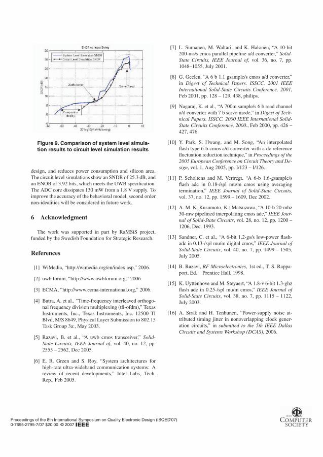
Figure 9. Comparison of system level simula-tion results to circuit level simulation results
design, and reduces power consumption and silicon area.The circuit level simulations show an SNDR of 25.3 dB, andan ENOB of 3.92 bits, which meets the UWB specification.The ADC core dissipates 130 mW from a 1.8 V supply. Toimprove the accuracy of the behavioral model, second ordernon-idealities will be considered in future work.
6 Acknowledgment
The work was supported in part by RaMSiS project,funded by the Swedish Foundation for Strategic Research.
References
[1] WiMedia, “http://wimedia.org/en/index.asp,” 2006.
[2] uwb forum, “http://www.uwbforum.org,” 2006.
[3] ECMA, “http://www.ecma-international.org,” 2006.
[4] Batra, A. et al., “Time-frequency interleaved orthogo-nal frequency division multiplexing (tfi-ofdm),” TexasInstruments, Inc., Texas Instruments, Inc. 12500 TIBlvd, M/S 8649, Physical Layer Submission to 802.15Task Group 3a:, May 2003.
[5] Razavi, B. et al., “A uwb cmos transceiver,” Solid-State Circuits, IEEE Journal of, vol. 40, no. 12, pp.2555 – 2562, Dec 2005.
[6] E. R. Green and S. Roy, “System architectures forhigh-rate ultra-wideband communication systems: Areview of recent developments,” Intel Labs, Tech.Rep., Feb 2005.
[7] L. Sumanen, M. Waltari, and K. Halonen, “A 10-bit200-ms/s cmos parallel pipeline a/d converter,” Solid-State Circuits, IEEE Journal of, vol. 36, no. 7, pp.1048–1055, July 2001.
[8] G. Geelen, “A 6 b 1.1 gsample/s cmos a/d converter,”in Digest of Technical Papers. ISSCC. 2001 IEEEInternational Solid-State Circuits Conference, 2001,Feb 2001, pp. 128 – 129, 438, philips.
[9] Nagaraj, K. et al., “A 700m sample/s 6 b read channela/d converter with 7 b servo mode,” in Digest of Tech-nical Papers. ISSCC. 2000 IEEE International Solid-State Circuits Conference, 2000., Feb 2000, pp. 426 –427, 476.
[10] Y. Park, S. Hwang, and M. Song, “An interpolatedflash type 6-b cmos a/d converter with a dc referencefluctuation reduction technique,” in Proceedings of the2005 European Conference on Circuit Theory and De-sign, vol. 1, Aug 2005, pp. I/123 – I/126.
[11] P. Scholtens and M. Vertregt, “A 6-b 1.6-gsample/sflash adc in 0.18-/spl mu/m cmos using averagingtermination,” IEEE Journal of Solid-State Circuits,vol. 37, no. 12, pp. 1599 – 1609, Dec 2002.
[12] A. M. K. Kusumoto, K.; Matsuzawa, “A 10-b 20-mhz30-mw pipelined interpolating cmos adc,” IEEE Jour-nal of Solid-State Circuits, vol. 28, no. 12, pp. 1200 –1206, Dec. 1993.
[13] Sandner, C. et al., “A 6-bit 1.2-gs/s low-power flash-adc in 0.13-/spl mu/m digital cmos,” IEEE Journal ofSolid-State Circuits, vol. 40, no. 7, pp. 1499 – 1505,July 2005.
[14] B. Razavi, RF Microelectronics, 1st ed., T. S. Rappa-port, Ed. Prentice Hall, 1998.
[15] K. Uyttenhove and M. Steyaert, “A 1.8-v 6-bit 1.3-ghzflash adc in 0.25-/spl mu/m cmos,” IEEE Journal ofSolid-State Circuits, vol. 38, no. 7, pp. 1115 – 1122,July 2003.
[16] A. Strak and H. Tenhunen, “Power-supply noise at-tributed timing jitter in nonoverlapping clock gener-ation circuits,” in submitted to the 5th IEEE DallasCircuits and Systems Workshop (DCAS), 2006.
Proceedings of the 8th International Symposium on Quality Electronic Design (ISQED'07)0-7695-2795-7/07 $20.00 © 2007

PAPER 2
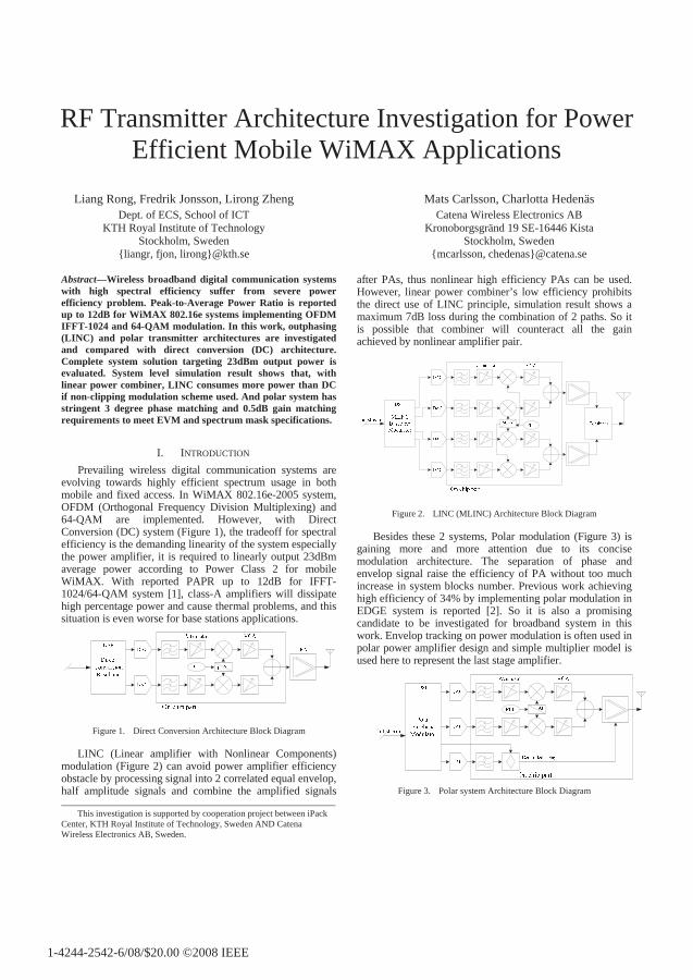
RF Transmitter Architecture Investigation for Power Efficient Mobile WiMAX Applications
Liang Rong, Fredrik Jonsson, Lirong Zheng Dept. of ECS, School of ICT
KTH Royal Institute of Technology Stockholm, Sweden
{liangr, fjon, lirong}@kth.se
Mats Carlsson, Charlotta Hedenäs Catena Wireless Electronics AB
Kronoborgsgränd 19 SE-16446 Kista Stockholm, Sweden
{mcarlsson, chedenas}@catena.se
Abstract—Wireless broadband digital communication systems with high spectral efficiency suffer from severe power efficiency problem. Peak-to-Average Power Ratio is reported up to 12dB for WiMAX 802.16e systems implementing OFDM IFFT-1024 and 64-QAM modulation. In this work, outphasing (LINC) and polar transmitter architectures are investigated and compared with direct conversion (DC) architecture. Complete system solution targeting 23dBm output power is evaluated. System level simulation result shows that, with linear power combiner, LINC consumes more power than DC if non-clipping modulation scheme used. And polar system has stringent 3 degree phase matching and 0.5dB gain matching requirements to meet EVM and spectrum mask specifications.
I. INTRODUCTION Prevailing wireless digital communication systems are
evolving towards highly efficient spectrum usage in both mobile and fixed access. In WiMAX 802.16e-2005 system, OFDM (Orthogonal Frequency Division Multiplexing) and 64-QAM are implemented. However, with Direct Conversion (DC) system (Figure 1), the tradeoff for spectral efficiency is the demanding linearity of the system especially the power amplifier, it is required to linearly output 23dBm average power according to Power Class 2 for mobile WiMAX. With reported PAPR up to 12dB for IFFT-1024/64-QAM system [1], class-A amplifiers will dissipate high percentage power and cause thermal problems, and this situation is even worse for base stations applications.
Figure 1. Direct Conversion Architecture Block Diagram
LINC (Linear amplifier with Nonlinear Components) modulation (Figure 2) can avoid power amplifier efficiency obstacle by processing signal into 2 correlated equal envelop, half amplitude signals and combine the amplified signals
after PAs, thus nonlinear high efficiency PAs can be used. However, linear power combiner’s low efficiency prohibits the direct use of LINC principle, simulation result shows a maximum 7dB loss during the combination of 2 paths. So it is possible that combiner will counteract all the gain achieved by nonlinear amplifier pair.
Figure 2. LINC (MLINC) Architecture Block Diagram
Besides these 2 systems, Polar modulation (Figure 3) is gaining more and more attention due to its concise modulation architecture. The separation of phase and envelop signal raise the efficiency of PA without too much increase in system blocks number. Previous work achieving high efficiency of 34% by implementing polar modulation in EDGE system is reported [2]. So it is also a promising candidate to be investigated for broadband system in this work. Envelop tracking on power modulation is often used in polar power amplifier design and simple multiplier model is used here to represent the last stage amplifier.
Figure 3. Polar system Architecture Block Diagram
This investigation is supported by cooperation project between iPack Center, KTH Royal Institute of Technology, Sweden AND Catena Wireless Electronics AB, Sweden.
1-4244-2542-6/08/$20.00 ©2008 IEEE
To compare 3 different architectures on the same basis, ADS simulation tool is used because it provides standard test sequence and signal sink modules for WiMAX (WMAN 802.16e) OFDM IFFT-1024/ 64-QAM system, standard EVM and spectrum evaluation is automatically carried out and power value can be calculated by spectrum analysis.
II. WIMAX SYSTEM SPECIFICATION Since WiMAX services are set as a replacement for cable
xDSL connection, it gains vast industrial support and a website called WiMAX Forum was founded for standardization purpose. On the other hand, as a broadband wireless air interface, WiMAX is also included as an IEEE 802.16 broadband wireless access standards member. So the specification is distributed in both places. Here a short summary of minimum requirements for WiMAX are cited.
A. Power Class Profile According to WiMAX Forum power class specification
[3], WiMAX mobile system (MS) devices are specified to output up to 23dBm power (class 2 for QAM16) and support a tunable TX dynamic range higher than 45dB. Detailed class category is quoted in Table I.
TABLE I. POWER CLASS PROFILE CLASSIFICATION
Class ID 16QAM Tx Pout(dBm) QPSK Tx Pout(dBm) Class 1 18 Tx,Pout<21 20 Tx,Pout<23 Class 2 21 Tx,Pout<25 23 Tx,Pout<27 Class 3 25 Tx,Pout<30 27 Tx,Pout<30 Class 4 30 Tx,Pout 30 Tx,Pout As for 64-QAM modulation, 23dBm is also set to be the
targeting output power and it is used as a comparison basis in the following context.
B. Frequency Band and Spectrum Mask After accepted as a formal 3G candidate in ITU-R in Oct.
2007, WiMAX now possess 2 frequency bands including 2.3GHz~2.4GHz (WiBro in Korea) and 2.496GHz~2.69GHz, they clip ISM-2400 band in both sides. To avoid out-of-band emission, WiMAX has very restricted spectrum mask requirements. Here 2 sets of spectrum mask is cited and presented in Table II, one is from ADS WMAN_16e_OFDMA design library and the other is from ITU-R M.1581 [4]. The values are converted to 10 kHz integration bandwidth. From this table, we can find ITU regulations are more restricted.
C. Relative Constellation Error (RCE) For high order modulation system like 64QAM, EVM is
required to be no greater than 3.1%, which converts to RCE of -30dB. Both ADS and IEEE Std 802.16e-2005 have same minimum EVM requirements for all profiles, so here in the system level analysis, highest performance is targeted. The EVM limitation is set to be -30dB to make it suitable for all lower data rate transmission burst types and spectrum mask results are checked to make sure the figure is complying with both requirements. The EVM value is achieved by ADS 802.16e EVM module with package frame of 5.
III. SYSTEM SIMULATION AND COMPARISON
A. Direct Conversion System Performance For direct conversion transmitter, due to the transmission
of wideband OFDM signal with large crest factor (Peak-to-Average Ratio), its last stage PA has to be placed at a large back-off position below 1dB compression point. So for DC system, PA’s P1dB simulation is compulsory. Besides, imbalance between IQ channels is also a dominant problem. Another signal quality degradation factor is PLL’s phase noise. In OFDM system, PLL’s noise will be integrated by multiple carriers and it will affect RCE as well. To simplify the simulation, an assumption is made on PA, its OIP3 is 9.6dB higher than P1dB and PA’s saturation output power is set to be 6dB lower than OIP3. Simulation result is shown in Figure 4 by sweeping PA’s OIP3.
Figure 4. RCE & Pout vs. PA’s OIP3 for Direct Conversion System
From simulation, in order to keep output power of 23dBm and EVM of -30dB, a linear amplifier with OIP3 of 38dBm should be used. While the spectrum mask is violated at 11MHz frequency offset in simulation and this can also be proved by manual calculation. A formal mathematical analysis on multi-tone intermodulation distortion can be
Direct Conversion RCE & Pout VS. OIP3
-45.0
-40.0
-35.0
-30.0
-25.0
-20.0
-15.0
30.0 34.0 38.0 42.0 46.0 50.0PA 3rd Order Intercept Point (OIP3) / dBm
RC
E (
dB
)
0.0
4.0
8.0
12.0
16.0
20.0
24.0
Pou
t (dB
m)
DC RCE (dB)
DC Pout (dBm)
TABLE II. SPECTRUM MASK FOR 10MHZ BANDWIDTH OFDM SIGNAL
Frequency Offset (MHz) from Fc Emission Level (dBm)
5 6 7.144 10 10.572 11 15 20 25 ADS -8 --- -32 --- -38 --- --- -50 -50
ITU-R M.1581* -7 -33 NA -33 --- -45 -48.58 -57 -57
--- No value specified in the offset point. * ITU regulation is for 2496MHz ~ 2690MHz band, value normalized to 10 kHz resolution bandwidth.
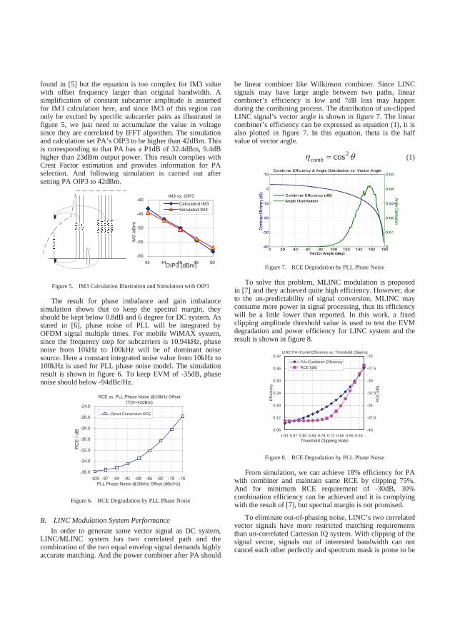
found in [5] but the equation is too complex for IM3 value with offset frequency larger than original bandwidth. A simplification of constant subcarrier amplitude is assumed for IM3 calculation here, and since IM3 of this region can only be excited by specific subcarrier pairs as illustrated in figure 5, we just need to accumulate the value in voltage since they are correlated by IFFT algorithm. The simulation and calculation set PA’s OIP3 to be higher than 42dBm. This is corresponding to that PA has a P1dB of 32.4dBm, 9.4dB higher than 23dBm output power. This result complies with Crest Factor estimation and provides information for PA selection. And following simulation is carried out after setting PA OIP3 to 42dBm.
IM3 vs. OIP3
-60
-55
-50
-45
-40
42 44 46 48 50OIP3 (dBm)
IM3
(d
Bm
)
Calculated IM3Simulated IM3
Figure 5. IM3 Calculation Illustration and Simulation with OIP3
The result for phase imbalance and gain imbalance simulation shows that to keep the spectral margin, they should be kept below 0.8dB and 6 degree for DC system. As stated in [6], phase noise of PLL will be integrated by OFDM signal multiple times. For mobile WiMAX system, since the frequency step for subcarriers is 10.94kHz, phase noise from 10kHz to 100kHz will be of dominant noise source. Here a constant integrated noise value from 10kHz to 100kHz is used for PLL phase noise model. The simulation result is shown in figure 6. To keep EVM of -35dB, phase noise should below -94dBc/Hz.
RCE vs. PLL Phase Noise @10kHz Offset(TOI=42dBm)
-36.0
-34.0
-32.0
-30.0
-28.0
-26.0
-24.0
-100 -97 -94 -91 -88 -85 -82 -79 -76PLL Phase Noise @10kHz Offset (dBc/Hz)
RC
E /
dB
Direct Conversion RCE
Figure 6. RCE Degradation by PLL Phase Noise
B. LINC Modulation System Performance In order to generate same vector signal as DC system,
LINC/MLINC system has two correlated path and the combination of the two equal envelop signal demands highly accurate matching. And the power combiner after PA should
be linear combiner like Wilkinson combiner. Since LINC signals may have large angle between two paths, linear combiner’s efficiency is low and 7dB loss may happen during the combining process. The distribution of un-clipped LINC signal’s vector angle is shown in figure 7. The linear combiner’s efficiency can be expressed as equation (1), it is also plotted in figure 7. In this equation, theta is the half value of vector angle.
2coscomb (1)
Figure 7. RCE Degradation by PLL Phase Noise
To solve this problem, MLINC modulation is proposed in [7] and they achieved quite high efficiency. However, due to the un-predictability of signal conversion, MLINC may consume more power in signal processing, thus its efficiency will be a little lower than reported. In this work, a fixed clipping amplitude threshold value is used to test the EVM degradation and power efficiency for LINC system and the result is shown in figure 8.
LINC PA+Comb Efficiency vs. Threshold Clipping
0.06
0.12
0.18
0.24
0.30
0.36
0.42
1.03 0.97 0.90 0.84 0.78 0.72 0.65 0.59 0.53Threshold Clipping Ratio
Effi
cien
cy
-40
-37.5
-35
-32.5
-30
-27.5
-25
RC
E (
dB)
PA+Combiner Efficiency
RCE (dB)
Figure 8. RCE Degradation by PLL Phase Noise
From simulation, we can achieve 18% efficiency for PA with combiner and maintain same RCE by clipping 75%. And for minimum RCE requirement of -30dB, 30% combination efficiency can be achieved and it is complying with the result of [7], but spectral margin is not promised.
To eliminate out-of-phasing noise, LINC’s two correlated vector signals have more restricted matching requirements than un-correlated Cartesian IQ system. With clipping of the signal vector, signals out of interested bandwidth can not cancel each other perfectly and spectrum mask is prone to be
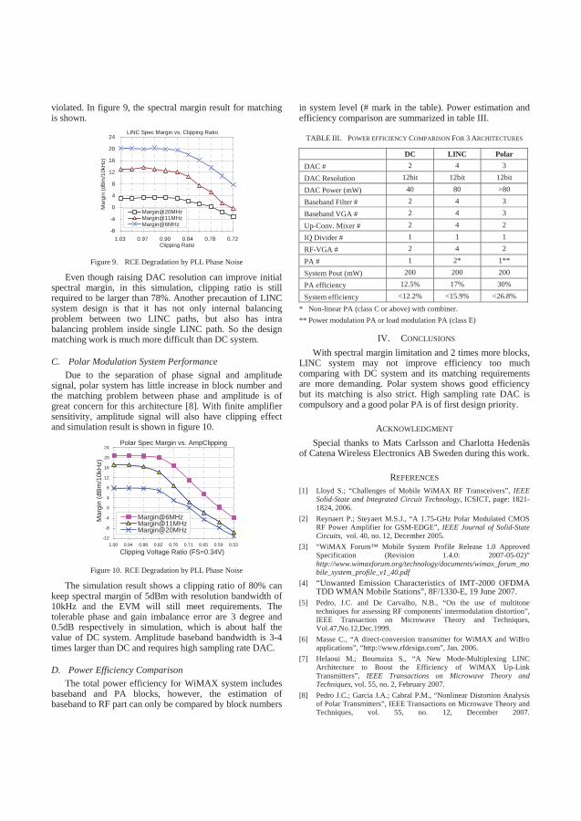
violated. In figure 9, the spectral margin result for matching is shown.
LINC Spec Margin vs. Clipping Ratio
-8
-4
0
4
8
12
16
20
24
1.03 0.97 0.90 0.84 0.78 0.72Clipping Ratio
Mar
gin
(dB
m/1
0kH
z)
Margin@20MHzMargin@11MHzMargin@6MHz
Figure 9. RCE Degradation by PLL Phase Noise
Even though raising DAC resolution can improve initial spectral margin, in this simulation, clipping ratio is still required to be larger than 78%. Another precaution of LINC system design is that it has not only internal balancing problem between two LINC paths, but also has intra balancing problem inside single LINC path. So the design matching work is much more difficult than DC system.
C. Polar Modulation System Performance Due to the separation of phase signal and amplitude
signal, polar system has little increase in block number and the matching problem between phase and amplitude is of great concern for this architecture [8]. With finite amplifier sensitivity, amplitude signal will also have clipping effect and simulation result is shown in figure 10.
Polar Spec Margin vs. AmpClipping
-12
-8
-4
0
4
8
12
16
20
24
1.00 0.94 0.88 0.82 0.76 0.71 0.65 0.59 0.53
Clipping Voltage Ratio (FS=0.34V)
Mar
gin
(dB
m/1
0kH
z)
Margin@6MHzMargin@11MHzMargin@20MHz
Figure 10. RCE Degradation by PLL Phase Noise
The simulation result shows a clipping ratio of 80% can keep spectral margin of 5dBm with resolution bandwidth of 10kHz and the EVM will still meet requirements. The tolerable phase and gain imbalance error are 3 degree and 0.5dB respectively in simulation, which is about half the value of DC system. Amplitude baseband bandwidth is 3-4 times larger than DC and requires high sampling rate DAC.
D. Power Efficiency Comparison The total power efficiency for WiMAX system includes
baseband and PA blocks, however, the estimation of baseband to RF part can only be compared by block numbers
in system level (# mark in the table). Power estimation and efficiency comparison are summarized in table III.
TABLE III. POWER EFFICIENCY COMPARISON FOR 3 ARCHITECTURES
DC LINC Polar DAC # 2 4 3
DAC Resolution 12bit 12bit 12bit
DAC Power (mW) 40 80 >80
Baseband Filter # 2 4 3
Baseband VGA # 2 4 3
Up-Conv. Mixer # 2 4 2
IQ Divider # 1 1 1
RF-VGA # 2 4 2
PA # 1 2* 1**
System Pout (mW) 200 200 200
PA efficiency 12.5% 17% 30%
System efficiency <12.2% <15.9% <26.8%
* Non-linear PA (class C or above) with combiner. ** Power modulation PA or load modulation PA (class E)
IV. CONCLUSIONS With spectral margin limitation and 2 times more blocks,
LINC system may not improve efficiency too much comparing with DC system and its matching requirements are more demanding. Polar system shows good efficiency but its matching is also strict. High sampling rate DAC is compulsory and a good polar PA is of first design priority.
ACKNOWLEDGMENT Special thanks to Mats Carlsson and Charlotta Hedenäs
of Catena Wireless Electronics AB Sweden during this work.
REFERENCES [1] Lloyd S.; “Challenges of Mobile WiMAX RF Transceivers”, IEEE
Solid-State and Integrated Circuit Technology, ICSICT, page: 1821-1824, 2006.
[2] Reynaert P.; Steyaert M.S.J., “A 1.75-GHz Polar Modulated CMOS RF Power Amplifier for GSM-EDGE”, IEEE Journal of Solid-State Circuits, vol. 40, no. 12, December 2005.
[3] “WiMAX Forum™ Mobile System Profile Release 1.0 Approved Specification (Revision 1.4.0: 2007-05-02)” http://www.wimaxforum.org/technology/documents/wimax_forum_mobile_system_profile_v1_40.pdf
[4] “Unwanted Emission Characteristics of IMT-2000 OFDMA TDD WMAN Mobile Stations”, 8F/1330-E, 19 June 2007.
[5] Pedro, J.C. and De Carvalho, N.B., “On the use of multitone techniques for assessing RF components' intermodulation distortion”, IEEE Transaction on Microwave Theory and Techniques, Vol.47,No.12,Dec.1999.
[6] Masse C., “A direct-conversion transmitter for WiMAX and WiBro applications”, “http://www.rfdesign.com”, Jan. 2006.
[7] Helaoui M.; Boumaiza S., “A New Mode-Multiplexing LINC Architecture to Boost the Efficiency of WiMAX Up-Link Transmitters”, IEEE Transactions on Microwave Theory and Techniques, vol. 55, no. 2, February 2007.
[8] Pedro J.C.; Garcia J.A.; Cabral P.M., “Nonlinear Distortion Analysis of Polar Transmitters”, IEEE Transactions on Microwave Theory and Techniques, vol. 55, no. 12, December 2007.

PAPER 3
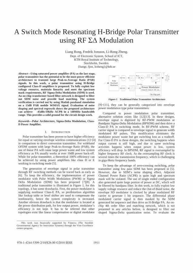
PolarBasebandModulator
On chip part
DSPDAC
DAC
PLL
Power ModulatorClass D / Class F / SF / etc.
Class E
Envelop
Phase
Figure 1 Traditional Polar Transmitter Architecture
A Switch Mode Resonating H-Bridge Polar Transmitter using RF Modulation
Liang Rong, Fredrik Jonsson, Li-Rong Zheng. Dept. of Electronic System, School of ICT,
KTH Royal Institute of Technology, Stockholm, Sweden.
{liangr, fjon, lrzheng}@kth.se
Abstract—Using saturated power amplifier (PA) as the last stage, polar transmitter has the potential to be the most power efficient architecture to transmit large Peak-to-Average Ratio (PAR) signals. In this work, a polar transmitter using H-Bridge configured Class-D amplifiers is proposed. To fully exploit low voltage resource, maintain linearity and meet the spectrum mask requirements, RF Sigma-Delta Modulation (SDM) is used. An on-chip transformer based filter network is designed to filter out SDM noise and provide load matching. The system verification is carried out by using Matlab passband simulation on a 13dB PAR mobile WiMAX signal. Evaluation of noise shaping and spectral regrowth shows the proposed architecture can achieve -45dBc/10kHz ACPR in a 140MHz bandwidth range. This provides a solid ground for the circuit design work.
Keywords—Polar Architecture, Sigma-Delta Modulation, Class-D Power Amplifier.
I. INTRODUCTION Polar transmitter has been proven to have higher efficiency
for equal or varying envelope wireless communications [1]~[4] in comparison to direct conversion transmitter. For wideband OFDM system with large Peak-to-Average Ratio (PAR), the use of linear PA will cause large power waste and low system efficiency as PA usually works at over 10dB power back-off. While for polar transmitter, a theoretical 100% efficiency can be achieved by using power amplifiers like class D or E working in switching mode [5].
The generation of envelope signal in polar transmitter through RF switching methods can be traced back as early as [6]. To keep the efficiency, the implementation of power modulator with Pulse Width Modulation (PWM) or Sigma Delta Modulation (SDM) has been proposed [7][8]. A traditional polar transmitter is illustrated in Figure 1, for this topology, it has some drawbacks. First, the power modulator is supplying nonlinear Class-E PA, so predistortion algorithm like lookup table or level shifter are used to compensate the nonlinearity, hence the system complexity is increased. Another obvious drawback is that the modulator is located at the power distribution path, for low output power, modulator’s efficiency is not kept. It has to be referred that other topologies exist like linear compensation or digital modulator
[9]~[11], they can be generally categorized into envelope power modulation type polar transmitters.
Compared to power modulation polar transmitter, alternative solution exists like [12][13]. In these designs, envelope signal is digitized by RF-PWM modulation or Bandpass Sigma-Delta Modulation (BPSDM) and then drive a Class-D PA in switching mode. In RF-PWM scheme, RF carrier signal is compared to envelope signal to generate width modulated RF pulses. This modification eliminates the modulator power waste but get switching loss as a tradeoff. For Class-D PA in these designs, the switching happens when output current is still high, and due to same switching activities happens when output power is low, system efficiency will drop. In BPSDM, RF signal is oversampled by higher frequency RF clock. As the oversampling RF clock is several times the transmission frequency, which is challenging in giga-Hertz frequency bands.
To keep the advantage of zero-crossing switching, polar transmitter using low pass SDM has been proposed in [5]. However, due to SDM’s noise shaping effect, Adjacent Channel Power Ratio (ACPR) is quite high and spectrum mask will be violated. The use of single ended configuration also generated quite large portion of power at DC, which will be filtered by bandpass filter. In this work, to fully exploit low supply voltage resource and reduce the Out-of-Band noise, the envelope SD modulator is clocked by phase modulated RF carrier to generate 1 bit sequence. The differential phase modulated carrier signal is then masked by the SDM generated bit sequence and then drive an H-Bridge PA. An on-chip 4th order filter and matching network, which is not presented in any articles before, is designed to filter out shaped Sigma-Delta quantization noise. To evaluate the
This work was financially supported by Vinnova (The SwedishGovernmental Agency for Innovation Systems) through the Vinn Excellencecenters program.
978-1-4244-5309-2/10/$26.00 ©2010 IEEE 1911
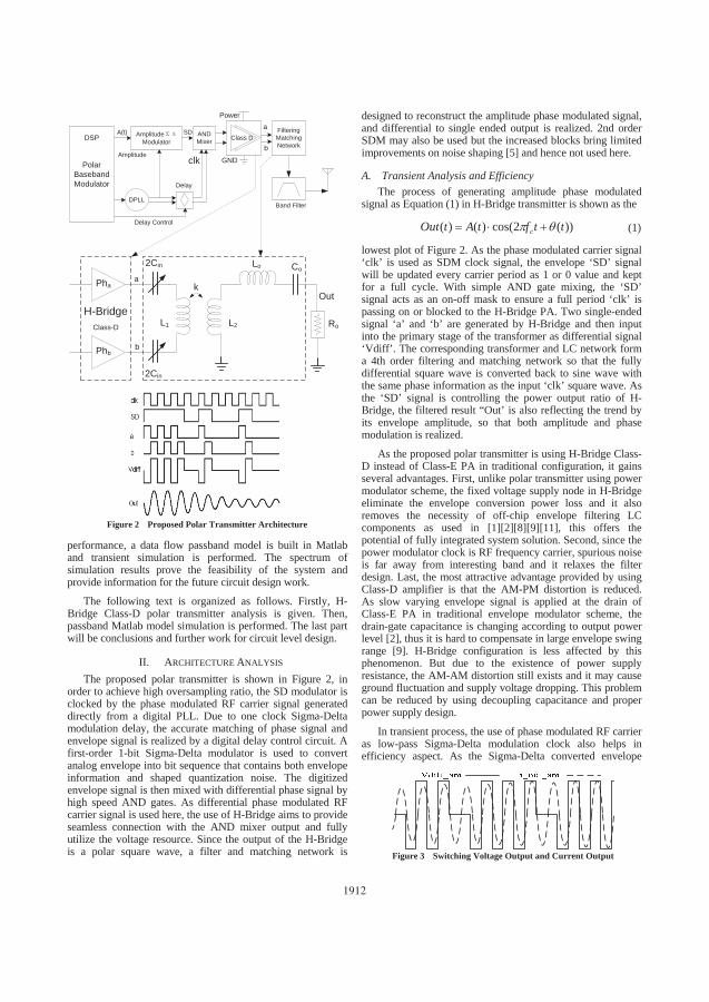
Figure 3 Switching Voltage Output and Current Output
performance, a data flow passband model is built in Matlab and transient simulation is performed. The spectrum of simulation results prove the feasibility of the system and provide information for the future circuit design work.
The following text is organized as follows. Firstly, H-Bridge Class-D polar transmitter analysis is given. Then, passband Matlab model simulation is performed. The last part will be conclusions and further work for circuit level design.
II. ARCHITECTURE ANALYSIS The proposed polar transmitter is shown in Figure 2, in
order to achieve high oversampling ratio, the SD modulator is clocked by the phase modulated RF carrier signal generated directly from a digital PLL. Due to one clock Sigma-Delta modulation delay, the accurate matching of phase signal and envelope signal is realized by a digital delay control circuit. A first-order 1-bit Sigma-Delta modulator is used to convert analog envelope into bit sequence that contains both envelope information and shaped quantization noise. The digitized envelope signal is then mixed with differential phase signal by high speed AND gates. As differential phase modulated RF carrier signal is used here, the use of H-Bridge aims to provide seamless connection with the AND mixer output and fully utilize the voltage resource. Since the output of the H-Bridge is a polar square wave, a filter and matching network is
designed to reconstruct the amplitude phase modulated signal, and differential to single ended output is realized. 2nd order SDM may also be used but the increased blocks bring limited improvements on noise shaping [5] and hence not used here.
A. Transient Analysis and Efficiency The process of generating amplitude phase modulated
signal as Equation (1) in H-Bridge transmitter is shown as the
))(2cos()()( ttftAtOut c (1)
lowest plot of Figure 2. As the phase modulated carrier signal ‘clk’ is used as SDM clock signal, the envelope ‘SD’ signal will be updated every carrier period as 1 or 0 value and kept for a full cycle. With simple AND gate mixing, the ‘SD’ signal acts as an on-off mask to ensure a full period ‘clk’ is passing on or blocked to the H-Bridge PA. Two single-ended signal ‘a’ and ‘b’ are generated by H-Bridge and then input into the primary stage of the transformer as differential signal ‘Vdiff’. The corresponding transformer and LC network form a 4th order filtering and matching network so that the fully differential square wave is converted back to sine wave with the same phase information as the input ‘clk’ square wave. As the ‘SD’ signal is controlling the power output ratio of H-Bridge, the filtered result “Out’ is also reflecting the trend by its envelope amplitude, so that both amplitude and phase modulation is realized.
As the proposed polar transmitter is using H-Bridge Class-D instead of Class-E PA in traditional configuration, it gains several advantages. First, unlike polar transmitter using power modulator scheme, the fixed voltage supply node in H-Bridge eliminate the envelope conversion power loss and it also removes the necessity of off-chip envelope filtering LC components as used in [1][2][8][9][11], this offers the potential of fully integrated system solution. Second, since the power modulator clock is RF frequency carrier, spurious noise is far away from interesting band and it relaxes the filter design. Last, the most attractive advantage provided by using Class-D amplifier is that the AM-PM distortion is reduced. As slow varying envelope signal is applied at the drain of Class-E PA in traditional envelope modulator scheme, the drain-gate capacitance is changing according to output power level [2], thus it is hard to compensate in large envelope swing range [9]. H-Bridge configuration is less affected by this phenomenon. But due to the existence of power supply resistance, the AM-AM distortion still exists and it may cause ground fluctuation and supply voltage dropping. This problem can be reduced by using decoupling capacitance and proper power supply design.
In transient process, the use of phase modulated RF carrier as low-pass Sigma-Delta modulation clock also helps in efficiency aspect. As the Sigma-Delta converted envelope
PolarBasebandModulator
DSP
DPLL
Amplitude
AmplitudeModulator
Power
GND
ANDMixer
Class D
Delay Control
Band Filter
Filtering MatchingNetwork
k
L2L1
2Cin
2Cin
Lo Co
Ro
H-BridgeClass-D
Pha
Phb
A(t)
clk
SD
a
b
Out
Delay
a
b
Figure 2 Proposed Polar Transmitter Architecture
1912
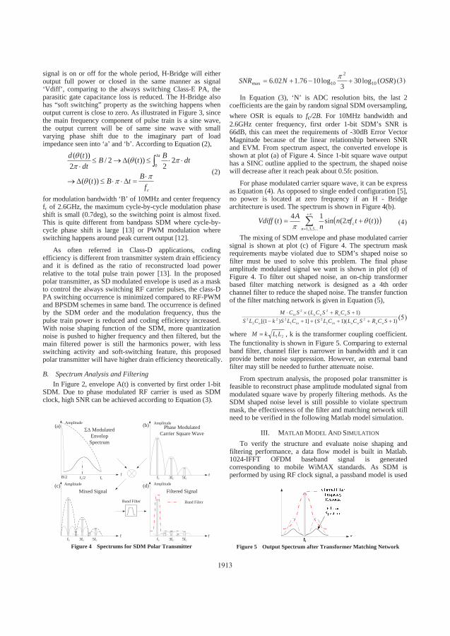
signal is on or off for the whole period, H-Bridge will either output full power or closed in the same manner as signal ‘Vdiff’, comparing to the always switching Class-E PA, the parasitic gate capacitance loss is reduced. The H-Bridge also has “soft switching” property as the switching happens when output current is close to zero. As illustrated in Figure 3, since the main frequency component of pulse train is a sine wave, the output current will be of same sine wave with small varying phase shift due to the imaginary part of load impedance seen into ‘a’ and ‘b’. According to Equation (2),
c
t
fBtBt
dtBtBdttd
))((
22
))((2/2
))((0
(2)
for modulation bandwidth ‘B’ of 10MHz and center frequency fc of 2.6GHz, the maximum cycle-by-cycle modulation phase shift is small (0.7deg), so the switching point is almost fixed. This is quite different from bandpass SDM where cycle-by-cycle phase shift is large [13] or PWM modulation where switching happens around peak current output [12].
As often referred in Class-D applications, coding efficiency is different from transmitter system drain efficiency and it is defined as the ratio of reconstructed load power relative to the total pulse train power [13]. In the proposed polar transmitter, as SD modulated envelope is used as a mask to control the always switching RF carrier pulses, the class-D PA switching occurrence is minimized compared to RF-PWM and BPSDM schemes in same band. The occurrence is defined by the SDM order and the modulation frequency, thus the pulse train power is reduced and coding efficiency increased. With noise shaping function of the SDM, more quantization noise is pushed to higher frequency and then filtered, but the main filtered power is still the harmonics power, with less switching activity and soft-switching feature, this proposed polar transmitter will have higher drain efficiency theoretically.
B. Spectrum Analysis and Filtering In Figure 2, envelope A(t) is converted by first order 1-bit
SDM. Due to phase modulated RF carrier is used as SDM clock, high SNR can be achieved according to Equation (3).
)(log303
log1076.102.6 10
2
10max OSRNSNR
In Equation (3), ‘N’ is ADC resolution bits, the last 2 coefficients are the gain by random signal SDM oversampling, where OSR is equals to fc/2B. For 10MHz bandwidth and 2.6GHz center frequency, first order 1-bit SDM’s SNR is 66dB, this can meet the requirements of -30dB Error Vector Magnitude because of the linear relationship between SNR and EVM. From spectrum aspect, the converted envelope is shown at plot (a) of Figure 4. Since 1-bit square wave output has a SINC outline applied to the spectrum, the shaped noise will decrease after it reach peak about 0.5fc position.
For phase modulated carrier square wave, it can be express as Equation (4). As opposed to single ended configuration [5], no power is located at zero frequency if an H - Bridge architecture is used. The spectrum is shown in Figure 4(b).
...5,3,1))((2sin14)(
nc ttfn
nAtVdiff
The mixing of SDM envelope and phase modulated carrier signal is shown at plot (c) of Figure 4. The spectrum mask requirements maybe violated due to SDM’s shaped noise so filter must be used to solve this problem. The final phase amplitude modulated signal we want is shown in plot (d) of Figure 4. To filter out shaped noise, an on-chip transformer based filter matching network is designed as a 4th order channel filter to reduce the shaped noise. The transfer function of the filter matching network is given in Equation (5),
)1)(1(]1)1[()1(
21
21
222
2
22
SCRSCLCLSCLSkCLSSCRSCLSCM
ooooinino
ooooin
where 21LLkM , k is the transformer coupling coefficient. The functionality is shown in Figure 5. Comparing to external band filter, channel filer is narrower in bandwidth and it can provide better noise suppression. However, an external band filter may still be needed to further attenuate noise.
From spectrum analysis, the proposed polar transmitter is feasible to reconstruct phase amplitude modulated signal from modulated square wave by properly filtering methods. As the SDM shaped noise level is still possible to violate spectrum mask, the effectiveness of the filter and matching network still need to be verified in the following Matlab model simulation.
III. MATLAB MODEL AND SIMULATION To verify the structure and evaluate noise shaping and
filtering performance, a data flow model is built in Matlab. 1024-IFFT OFDM baseband signal is generated corresponding to mobile WiMAX standards. As SDM is performed by using RF clock signal, a passband model is used f
Amplitude
Modulated Envelop
Spectrum
f
Amplitude
fc 3fc 5fc
Phase Modulated Carrier Square Wave
Amplitude
fc 3fc 5fc
Mixed Signal
Band Filter
B/2 fc/2Amplitude
fc 3fc 5fc
Filtered Signal
Band Filter
fc
(a)
f f
(b)
(c) (d)
Figure 4 Spectrums for SDM Polar Transmitter
Figure 5 Output Spectrum after Transformer Matching Network
1913
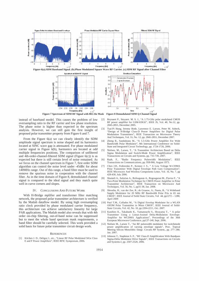
instead of baseband model. This causes the problem of low oversampling ratio to the RF carrier and low phase resolution. The phase noise is higher than expected in the spectrum analysis. However, we can still gain the first insight of proposed polar transmitter property from Figure 6 and 7.
From the Figure 6(a) we can clearly identify the SDM amplitude signal spectrum is noise shaped and its harmonics located at SINC wave gap is attenuated. For phase modulated carrier signal in Figure 6(b), harmonics are located at odd multiple frequencies positions. The comparison of unfiltered and 4th-order-channel-filtered SDM signal (Figure 6(c)) is as expected but there is still certain level of noise remained. As we focus on the channel spectrum in Figure 7, first order SDM algorithm can control the noise level under -45dBc for about 140MHz range. Out of this range, a band filter must be used to remove the spurious noise in cooperation with the channel filter. As in the time domain of Figure 8, demodulated channel signal is compared to the ideal signal and they match quite well in curve corners and slopes.
IV. CONCLUSIONS AND FUTURE WORK With H-Bridge mplifier and transformer filter matching
network, the proposed polar transmitter architecture is verified by the Matlab dataflow model. By using high oversampling ratio clock provided by phase modulated carrier frequency, this architecture can achieve satisfactory linearity for large PAR applications. The Matlab model also reveals that with 4th order on-chip filtering, out-of-band noise can be suppressed but to meet the whole band spectrum mask requirements, a band filter should be carefully selected. This work provided a solid basis for future polar transmitter circuit design work.
REFERENCES [1] Kitchen J. D., Deligoz I., etc., “Linear RF Polar Modulated SiGe Class
E and F Power Amplifiers”, IEEE RFIC Symposium, 2006.
[2] Reynaert P., Steyaert. M. S. J., “A 1.75-GHz polar modulated CMOS RF power amplifier for GSM-EDGE”, IEEE JS, Vol. 40, No.12, pp. 2845-2855, December 2005.
[3] Tsai-Pi Hung, Jeremy Rode, Lawrence E. Larson, Peter M. Asbeck, “Design of H-Bridge Class-D Power Amplifiers for Digital Pulse Modulation Transmitters”, IEEE Transaction on Microwave Theory And Techniques, Vol. 55, No. 12, pp. 2845-2855, December 2007.
[4] Zheng R., Sanduleanu M., “A 5.5-GHz Power Amplifier For Wide Bandwidth Polar Modulator”, 8th International Conference on Solid-State and Integrated Circuit Technology, pp. 1724-1726, 2006.
[5] Nielsen, M., Larsen, T., “A Transmitter Architecture Based on Delta Sigma Modulation and Switch-Mode Power Amplification”, IEEE Transactions on Circuits and Systems, pp. 735-739, 2007.
[6] Raab, F., “Radio Frequency Pulsewidth Modulation”, IEEE Transactions on Communications, pp. 958-966, August 1973.
[7] Chen J.H., Fedorenko P., Kenney J. S., “ A Low Voltage W-CDMA Polar Transmitter With Digital Envelope Path Gain Compensation”, IEEE Microwave And Wireless Components Letter, Vol. 16, No. 7, pp 428-430, July 2006.
[8] Shameli A., Safarian A., Rofougaran A., Rogougaran M., Flaviss F., ”A Two-Point Modulation Technique for CMOS Power Amplifier in Polar Transmitter Architecture”, IEEE Transaction on Microwave And Techniques, Vol. 56, No. 1, pp31-38, Jan. 2008.
[9] Shrestha, R.; van der Zee, R.; de Graauw, A.; Nauta, B., “A Wideband Supply Modulator for 20 MHz RF Bandwidth Polar PAs in 65 nm CMOS”, IEEE Journal of Solid State Circuits, Vol 44, pp1272 – 1280, April 2009
[10] Paul T.M., Collados M., “A Digital Envelop Modulator for a WLAN OFDM Polar Transmitter in 90nm CMOS”, IEEE Journal of Solid-State Circuits, Vol. 42, No. 10, pp 2204-2211, Oct. 2007.
[11] Kunihiro K., Takahashi K., Yamanouchi S., Hirayama T., “ A polar Transmitter Using a Linear-Assited Delta-Modulation Envelope-Amplifier for WCDMA Applications”, Proceedings of the 36th European Microwave Conference, pp137-140, Sept. 2006.
[12] Nielsen M., Larsen T., “An RF pulsewidth modulator for switchmode power amplification of varying envelope signals”, Proc. Topical Meeting Silicon Monolithic Integr. Circuits RF System., pp. 277–280, Jan. 2007.
[13] Johnson T., Stapleton S. P., “RF Class-D Amplification With Bandpass Sigma-Delta Modulator Drive Signals”, IEEE Transactions on Circuits and Systems-I, pp. 2507-2520, 2006.
Figure 6(a).SDM Baseband Signal. (b).Phase Modulated Square Wave RF Carrier. (c).SDM RF Signal after Channel Filter
Figure 7 Spectrum of SDM RF Signal with 802.16e Mask Figure 8 Demodulated SDM Q-Channel Signal
1914

PAPER 4
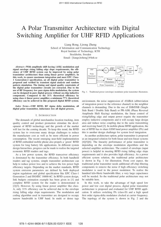
A Polar Transmitter Architecture with DigitalSwitching Amplifier for UHF RFID Applications
Liang Rong, Lirong ZhengSchool of Information and Communication Technology
Royal Institute of Technology, KTH
Stockholm, Sweden
Email: {liangr,lrzheng}@kth.se
Abstract—With amplitude shift keying (ASK) modulation andsignal envelope rising falling edge slope requirements, the effi-ciency of UHF RFID system can be improved by using polartransmitter architecture than using linear power amplifiers. Inthis work, to ensure maximum integration and meet EPC Class-1 Generation-2 specification, an all digital polar transmitter isproposed and verified by transient signal analysis and randompattern simulation. The timing and signal quality constraints ofthe digital polar transmitter circuits are extracted. Due to theuse of RF frequency low pass sigma delta modulation, the systemcan be designed in pure digital process without on-chip inductivecomponents. Compared to the 31% theoretical efficiency byusing class-A linear power amplifier, a minimum 77% theoreticalefficiency can be achieved in this proposed digital RFID system.
Index Terms—UHF RFID, RF sigma delta modulation, alldigital polar transmitter, inductance less all digital process.
I. INTRODUCTION
The demands of global merchandise location tracking, item
quality control and product promotion stimulate the devel-
opment of RFID technology and the growth of the market
will last for the coming decade. To keep this trend, the RFID
system has to overcome many design challenges to reduce
the manufacture cost as well as be more efficient in power
consumption. The recent emerging near-field implementation
of RFID embedded mobile phone also propels a ’green’ RFID
system for long battery life applications. In different system
design hierarchies, progress can be made to realize the targeted
economic RFID readers and tags.
As a low power system, the RFID transceiver efficiency
is dominated by the transmitter efficiency. In both handheld
readers and tag systems, simple transmitter architecture can
help to reduce power loss and to achieve the low power high
efficiency targets. Depending on the market standards, RFID
system emission parameters are defined by both deployed
region regulations and global specification like EPC Class-1
Generation-2 and ISO/IEC 18000-6C. In RFID system design,
link budgets estimation example has been given in [1] and
complete RFID system for the reader is demonstrated in
[2][3]. However, by using linear power amplifier like class-
A, only 31% efficiency can be achieved due to the envelope
rising falling edge slope requirements. The modulation and
coding algorithm used in transmitter are designed to occupy
narrow bandwidth in UHF band. In multi or dense tags
Polar Transmitter
PLL
PowerModulator
Class E
Envelop
PolarBasebandModulator
DSP
)()( 22 tQtI �
),( ��f
off-chipLC filter
UHFbandpass
filter
Fig. 1. Traditional power (envelope) modulator polar transmitter illustration.
environment, the noise suppression of -65dBch (abbreviation
of integration power to the reference channel) to the neighbor
channels is demanding. Due to the use of SSB/DSB (Single
Side Band / Double Side Band) or PR-ASK (Phase Reversal
Amplitude Shift Keying) modulation, the linear control of
rising/falling edge and output power require the transmitter
employ inductive components and it will occupy large design
area and induce noise coupling due to the same transmitting
and receiving band [2]. In mobile-phone RFID application, the
use of RFID has to share GSM band power amplifier (PA) and
this is another design challenge for system level integration.
As another architecture option, polar transmitter is proposed
as an integrated solution for both linear and non-linear systems
[4][5][6]. The linearity performance of polar transmitter is
depending on the envelope modulation algorithms and the
selected amplifier architecture. The control of envelope (input
power) is helpful in meeting RFID rising falling edge slope
requirements and it also provides high efficiency. As a power
efficient system solution, the traditional polar architecture
is shown in Fig. 1 for illustration. From cost aspect, the
traditional polar transmitter needs additional off-chip filtering
components to remove the noise if high efficiency switching
modulator is used in the power modulator. To realize the
hundred kilo-Hertz bandwidth filter, a very large capacitance
will be needed. So the traditional polar architecture may not
be suitable here.
In this work, to take the advantage of high speed low
power and low cost digital process, digital polar transmitter
architecture is proposed and evaluated for UHF RFID appli-
cation. It utilizes switching PA (class-D) and a high speed
first order sigma-delta modulator clocked at carrier frequency.
The topology of the system is shown in Fig. 2 and the
2011 IEEE International Conference on RFID
978-1-4244-9606-8/11/$26.00 ©2011 IEEE 128
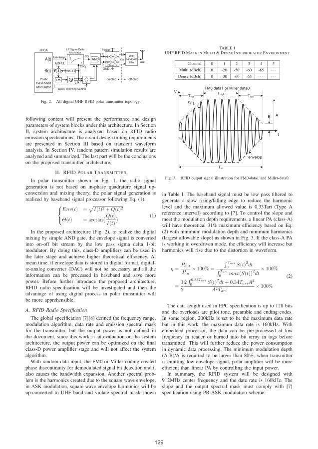
FPGA
Envelop
Power
GNDClass D
Delay Trimming Control
UHFbandpass
filterA(t)
clk
SDa
b
Θ(t)ADPLL Out
+Vdiff
-AND
LP Sigma DeltaModulator
LPC
TDC & Σ-
PolarBasebandModulator
clkp
off-chipon-chip
Fig. 2. All digital UHF RFID polar transmitter topology.
following content will present the performance and design
parameters of system blocks under this architecture. In Section
II, system architecture is analyzed based on RFID radio
emission specifications. The circuit design timing requirements
are presented in Section III based on transient waveform
analysis. In Section IV, random pattern simulation results are
analyzed and summarized. The last part will be the conclusions
on the proposed transmitter architecture.
II. RFID POLAR TRANSMITTER
In polar transmitter shown in Fig. 1, the radio signal
generation is not based on in-phase quadrature signal up-
conversion and mixing theory, the polar signal generation is
realized by baseband signal processor following Eq. (1).⎧⎨⎩Env(t) =
√I(t)2 +Q(t)2
Θ(t) = arctan(Q(t)
I(t)
) (1)
In the proposed architecture (Fig. 2), to realize the digital
mixing by simple AND gate, the envelope signal is converted
into on-off bit stream by the low pass sigma delta 1-bit
modulator. By doing this, class-D amplifiers can be used in
the later stage and achieve higher theoretical efficiency. At
mean time, if envelope data is stored in digital format, digital-
to-analog converter (DAC) will not be necessary and all the
information can be processed in baseband and save more
power. Before further introduce the proposed architecture,
RFID radio specification will be investigated and then the
advantage of using digital process in polar transmitter will
be more apprehensible.
A. RFID Radio Specification
The global specification [7][8] defined the frequency range,
modulation algorithm, data rate and emission spectral mask
for the transmitter, but the output power is not defined in
the document, since this work is an evaluation on the system
architecture, the output power can be optimized on the final
class-D power amplifier stage and will not affect the system
algorithm.
With random data input, the FM0 or Miller coding created
phase discontinuity for demodulated signal bit detection and it
also causes the bandwidth expansion. Another spectral prob-
lem is the harmonics created due to the square wave envelope,
in ASK modulation, square wave envelope harmonics will be
up-converted to UHF band and violate spectral mask shown
TABLE IUHF RFID MASK IN MULTI & DENSE INTERROGATOR ENVIRONMENT
Channel 0 1 2 3 4 5
Multi (dBch) 0 -20 -50 -60 -65 · · ·Dense (dBch) 0 -30 -60 -65 · · · · · ·
envelop
TfallThighTrise
Tari
B A
FM0 data1 or Miller data0
t
V
S(t)
Fig. 3. RFID output signal illustration for FM0-data1 and Miller-data0.
in Table I. The baseband signal must be low pass filtered to
generate a slow rising/falling edge to reduce the harmonic
level and the maximum allowed value is 0.33Tari (Type A
reference interval) according to [7]. To control the slope and
meet the modulation depth requirements, a linear PA (class-A)
will have theoretical 31% maximum efficiency based on Eq.
(2) with minimum modulation depth and minimum harmonics
(largest allowable slope) as shown in Fig. 3. If the class-A PA
is working in overdriven mode, the efficiency will increase but
harmonics will rise due to the distortion in waveform.
η =Pout
Pin× 100% =
∫ Tari
0S(t)
2dt∫ Tari
0max(S(t))
2dt
× 100%
=1
2
2∫ 0.33Tari
0S(t)
2dt+ 0.34TariA
2
A2Tari× 100%
(2)
The data length used in EPC specification is up to 128 bits
and the overloads are pilot tone, preamble and ending codes.
In some region, 200kHz is set to be the maximum data rate
but in this work, the maximum data rate is 160kHz. With
embedded processor, the data can be pre-processed at low
frequency in reader or burned into bit array in tags before
transmitted. This will further reduce the power consumption
in dynamic data processing. The minimum modulation depth
(A-B)/A is required to be larger than 80%, when transmitter
is emitting low envelope signal, polar amplifier will be more
efficient than linear PA by controlling the input power.
In summary, the RFID system will be designed with
912MHz center frequency and the date rate is 160kHz. The
slope and the output spectral mask must comply with [7]
specification using PR-ASK modulation scheme.
129
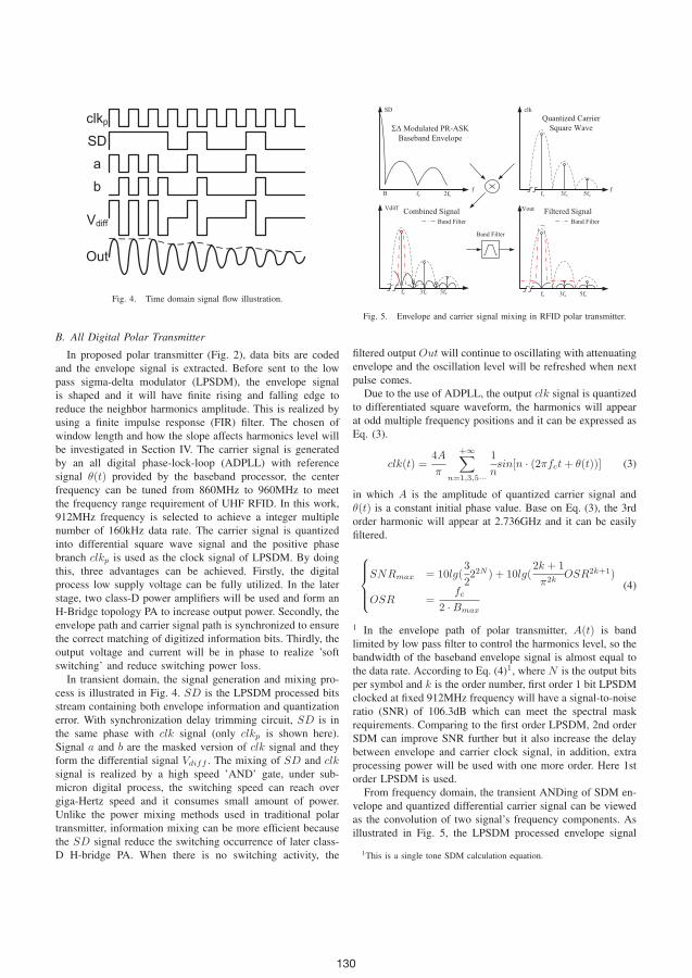
ab
clkp
SD
Vdiff
Out
Fig. 4. Time domain signal flow illustration.
B. All Digital Polar Transmitter
In proposed polar transmitter (Fig. 2), data bits are coded
and the envelope signal is extracted. Before sent to the low
pass sigma-delta modulator (LPSDM), the envelope signal
is shaped and it will have finite rising and falling edge to
reduce the neighbor harmonics amplitude. This is realized by
using a finite impulse response (FIR) filter. The chosen of
window length and how the slope affects harmonics level will
be investigated in Section IV. The carrier signal is generated
by an all digital phase-lock-loop (ADPLL) with reference
signal θ(t) provided by the baseband processor, the center
frequency can be tuned from 860MHz to 960MHz to meet
the frequency range requirement of UHF RFID. In this work,
912MHz frequency is selected to achieve a integer multiple
number of 160kHz data rate. The carrier signal is quantized
into differential square wave signal and the positive phase
branch clkp is used as the clock signal of LPSDM. By doing
this, three advantages can be achieved. Firstly, the digital
process low supply voltage can be fully utilized. In the later
stage, two class-D power amplifiers will be used and form an
H-Bridge topology PA to increase output power. Secondly, the
envelope path and carrier signal path is synchronized to ensure
the correct matching of digitized information bits. Thirdly, the
output voltage and current will be in phase to realize ’soft
switching’ and reduce switching power loss.
In transient domain, the signal generation and mixing pro-
cess is illustrated in Fig. 4. SD is the LPSDM processed bits
stream containing both envelope information and quantization
error. With synchronization delay trimming circuit, SD is in
the same phase with clk signal (only clkp is shown here).
Signal a and b are the masked version of clk signal and they
form the differential signal Vdiff . The mixing of SD and clksignal is realized by a high speed ’AND’ gate, under sub-
micron digital process, the switching speed can reach over
giga-Hertz speed and it consumes small amount of power.
Unlike the power mixing methods used in traditional polar
transmitter, information mixing can be more efficient because
the SD signal reduce the switching occurrence of later class-
D H-bridge PA. When there is no switching activity, the
f
SD
ΣΔModulated PR-ASKBaseband Envelope
f
clk
fc 3fc 5fc
Quantized CarrierSquare Wave
Vdiff
fc 3fc 5fc
Combined SignalBand Filter
B
Band Filter
Vout
fc 3fc 5fc
Filtered SignalBand Filter
fc 2fc
Fig. 5. Envelope and carrier signal mixing in RFID polar transmitter.
filtered output Out will continue to oscillating with attenuating
envelope and the oscillation level will be refreshed when next
pulse comes.
Due to the use of ADPLL, the output clk signal is quantized
to differentiated square waveform, the harmonics will appear
at odd multiple frequency positions and it can be expressed as
Eq. (3).
clk(t) =4A
π
+∞∑n=1,3,5···
1
nsin[n · (2πfct+ θ(t))] (3)
in which A is the amplitude of quantized carrier signal and
θ(t) is a constant initial phase value. Base on Eq. (3), the 3rd
order harmonic will appear at 2.736GHz and it can be easily
filtered.
⎧⎪⎪⎨⎪⎪⎩SNRmax = 10lg(
3
222N ) + 10lg(
2k + 1
π2kOSR2k+1)
OSR =fc
2 ·Bmax
(4)
1 In the envelope path of polar transmitter, A(t) is band
limited by low pass filter to control the harmonics level, so the
bandwidth of the baseband envelope signal is almost equal to
the data rate. According to Eq. (4)1, where N is the output bits
per symbol and k is the order number, first order 1 bit LPSDM
clocked at fixed 912MHz frequency will have a signal-to-noise
ratio (SNR) of 106.3dB which can meet the spectral mask
requirements. Comparing to the first order LPSDM, 2nd order
SDM can improve SNR further but it also increase the delay
between envelope and carrier clock signal, in addition, extra
processing power will be used with one more order. Here 1st
order LPSDM is used.
From frequency domain, the transient ANDing of SDM en-
velope and quantized differential carrier signal can be viewed
as the convolution of two signal’s frequency components. As
illustrated in Fig. 5, the LPSDM processed envelope signal
1This is a single tone SDM calculation equation.
130
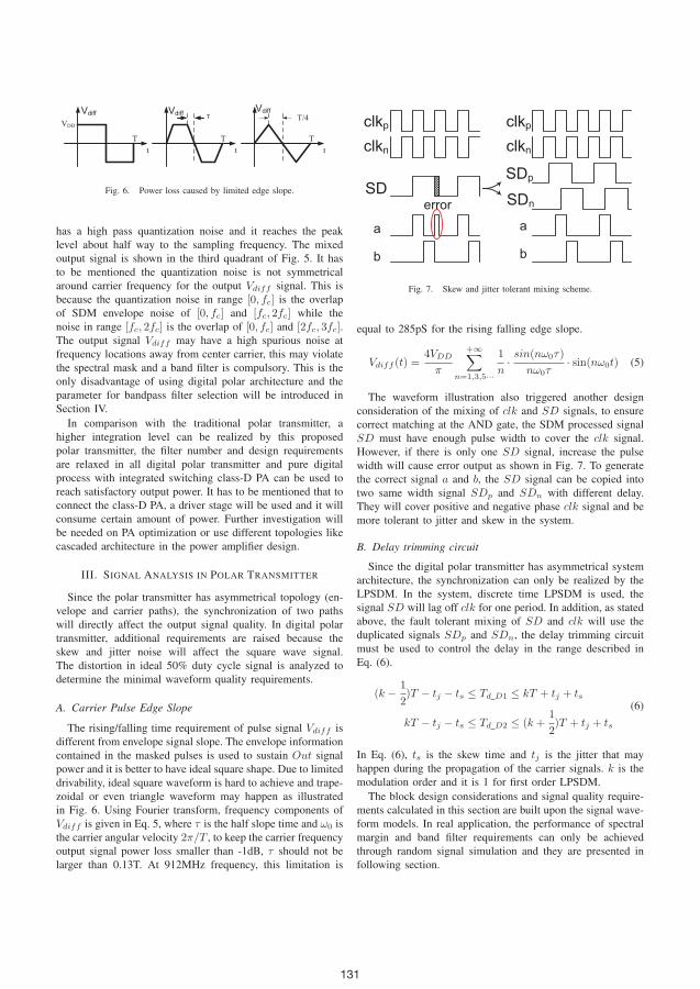
Tt
T
τ
tT
T/4
t
VDDVdiff Vdiff Vdiff
Fig. 6. Power loss caused by limited edge slope.
has a high pass quantization noise and it reaches the peak
level about half way to the sampling frequency. The mixed
output signal is shown in the third quadrant of Fig. 5. It has
to be mentioned the quantization noise is not symmetrical
around carrier frequency for the output Vdiff signal. This is
because the quantization noise in range [0, fc] is the overlap
of SDM envelope noise of [0, fc] and [fc, 2fc] while the
noise in range [fc, 2fc] is the overlap of [0, fc] and [2fc, 3fc].The output signal Vdiff may have a high spurious noise at
frequency locations away from center carrier, this may violate
the spectral mask and a band filter is compulsory. This is the
only disadvantage of using digital polar architecture and the
parameter for bandpass filter selection will be introduced in
Section IV.
In comparison with the traditional polar transmitter, a
higher integration level can be realized by this proposed
polar transmitter, the filter number and design requirements
are relaxed in all digital polar transmitter and pure digital
process with integrated switching class-D PA can be used to
reach satisfactory output power. It has to be mentioned that to
connect the class-D PA, a driver stage will be used and it will
consume certain amount of power. Further investigation will
be needed on PA optimization or use different topologies like
cascaded architecture in the power amplifier design.
III. SIGNAL ANALYSIS IN POLAR TRANSMITTER
Since the polar transmitter has asymmetrical topology (en-
velope and carrier paths), the synchronization of two paths
will directly affect the output signal quality. In digital polar
transmitter, additional requirements are raised because the
skew and jitter noise will affect the square wave signal.
The distortion in ideal 50% duty cycle signal is analyzed to
determine the minimal waveform quality requirements.
A. Carrier Pulse Edge Slope
The rising/falling time requirement of pulse signal Vdiff is
different from envelope signal slope. The envelope information
contained in the masked pulses is used to sustain Out signal
power and it is better to have ideal square shape. Due to limited
drivability, ideal square waveform is hard to achieve and trape-
zoidal or even triangle waveform may happen as illustrated
in Fig. 6. Using Fourier transform, frequency components of
Vdiff is given in Eq. 5, where τ is the half slope time and ω0 is
the carrier angular velocity 2π/T , to keep the carrier frequency
output signal power loss smaller than -1dB, τ should not be
larger than 0.13T. At 912MHz frequency, this limitation is
clkp
SD
clkn
a
b
clkp
clkn
a
b
SDp
SDnerror
Fig. 7. Skew and jitter tolerant mixing scheme.
equal to 285pS for the rising falling edge slope.
Vdiff (t) =4VDD
π
+∞∑n=1,3,5···
1
n· sin(nω0τ)
nω0τ· sin(nω0t) (5)
The waveform illustration also triggered another design
consideration of the mixing of clk and SD signals, to ensure
correct matching at the AND gate, the SDM processed signal
SD must have enough pulse width to cover the clk signal.
However, if there is only one SD signal, increase the pulse
width will cause error output as shown in Fig. 7. To generate
the correct signal a and b, the SD signal can be copied into
two same width signal SDp and SDn with different delay.
They will cover positive and negative phase clk signal and be
more tolerant to jitter and skew in the system.
B. Delay trimming circuit
Since the digital polar transmitter has asymmetrical system
architecture, the synchronization can only be realized by the
LPSDM. In the system, discrete time LPSDM is used, the
signal SD will lag off clk for one period. In addition, as stated
above, the fault tolerant mixing of SD and clk will use the
duplicated signals SDp and SDn, the delay trimming circuit
must be used to control the delay in the range described in
Eq. (6).
(k − 1
2)T − tj − ts ≤ Td D1 ≤ kT + tj + ts
kT − tj − ts ≤ Td D2 ≤ (k +1
2)T + tj + ts
(6)
In Eq. (6), ts is the skew time and tj is the jitter that may
happen during the propagation of the carrier signals. k is the
modulation order and it is 1 for first order LPSDM.
The block design considerations and signal quality require-
ments calculated in this section are built upon the signal wave-
form models. In real application, the performance of spectral
margin and band filter requirements can only be achieved
through random signal simulation and they are presented in
following section.
131
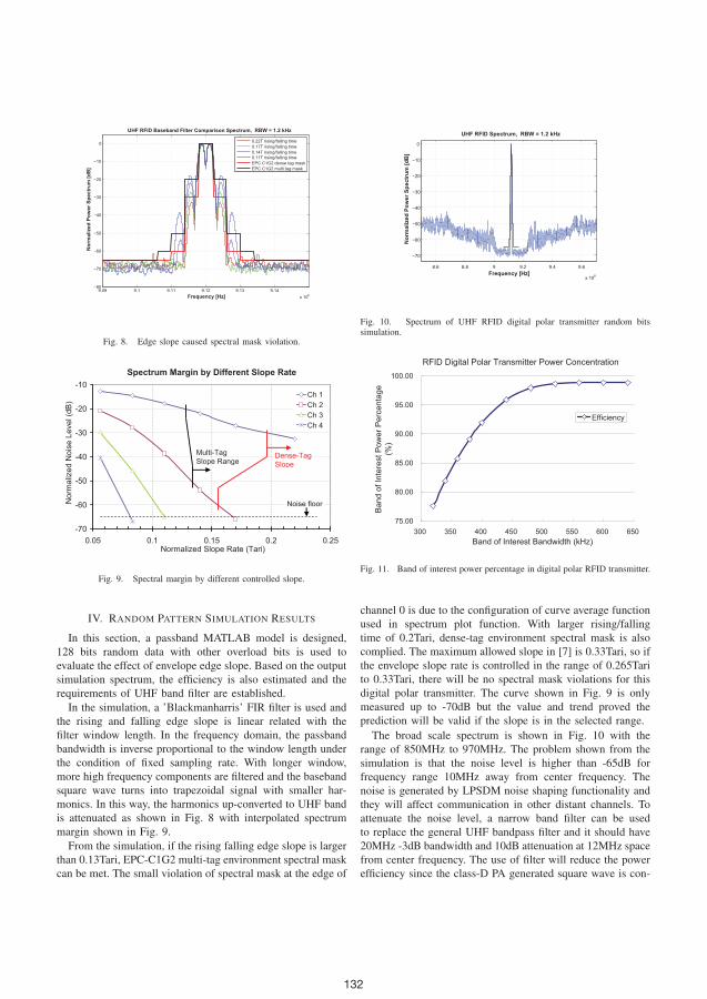
���� ��� ���� ���� ���� �������
���
� �
���
���
���
���
���
���
�
Frequency [Hz]
Nor
mal
ized
Pow
er S
pect
rum
[dB
]
UHF RFID Baseband Filter Comparison Spectrum, RBW = 1.2 kHz
�������������������������� ���������������������������������������������������������������������� �!����������"����� ��#���������"
Fig. 8. Edge slope caused spectral mask violation.
Spectrum Margin by Different Slope Rate
-70
-60
-50
-40
-30
-20
-10
0.05 0.1 0.15 0.2 0.25Normalized Slope Rate (Tari)
Nor
mal
ized
Noi
se L
evel
(dB
)
Ch 1Ch 2Ch 3Ch 4
Multi-TagSlope Range
Dense-TagSlope
Noise floor
Fig. 9. Spectral margin by different controlled slope.
IV. RANDOM PATTERN SIMULATION RESULTS
In this section, a passband MATLAB model is designed,
128 bits random data with other overload bits is used to
evaluate the effect of envelope edge slope. Based on the output
simulation spectrum, the efficiency is also estimated and the
requirements of UHF band filter are established.
In the simulation, a ’Blackmanharris’ FIR filter is used and
the rising and falling edge slope is linear related with the
filter window length. In the frequency domain, the passband
bandwidth is inverse proportional to the window length under
the condition of fixed sampling rate. With longer window,
more high frequency components are filtered and the baseband
square wave turns into trapezoidal signal with smaller har-
monics. In this way, the harmonics up-converted to UHF band
is attenuated as shown in Fig. 8 with interpolated spectrum
margin shown in Fig. 9.
From the simulation, if the rising falling edge slope is larger
than 0.13Tari, EPC-C1G2 multi-tag environment spectral mask
can be met. The small violation of spectral mask at the edge of
8.6 8.8 9 9.2 9.4 9.6
x 108
−70
−60
−50
−40
−30
−20
−10
0
Frequency [Hz]
Nor
mal
ized
Pow
er S
pect
rum
[dB
]
UHF RFID Spectrum, RBW = 1.2 kHz
Fig. 10. Spectrum of UHF RFID digital polar transmitter random bitssimulation.
RFID Digital Polar Transmitter Power Concentration
75.00
80.00
85.00
90.00
95.00
100.00
300 350 400 450 500 550 600 650Band of Interest Bandwidth (kHz)
Ban
d of
Inte
rest
Pow
er P
erce
ntag
e(%
)
Efficiency
Fig. 11. Band of interest power percentage in digital polar RFID transmitter.
channel 0 is due to the configuration of curve average function
used in spectrum plot function. With larger rising/falling
time of 0.2Tari, dense-tag environment spectral mask is also
complied. The maximum allowed slope in [7] is 0.33Tari, so if
the envelope slope rate is controlled in the range of 0.265Tari
to 0.33Tari, there will be no spectral mask violations for this
digital polar transmitter. The curve shown in Fig. 9 is only
measured up to -70dB but the value and trend proved the
prediction will be valid if the slope is in the selected range.
The broad scale spectrum is shown in Fig. 10 with the
range of 850MHz to 970MHz. The problem shown from the
simulation is that the noise level is higher than -65dB for
frequency range 10MHz away from center frequency. The
noise is generated by LPSDM noise shaping functionality and
they will affect communication in other distant channels. To
attenuate the noise level, a narrow band filter can be used
to replace the general UHF bandpass filter and it should have
20MHz -3dB bandwidth and 10dB attenuation at 12MHz space
from center frequency. The use of filter will reduce the power
efficiency since the class-D PA generated square wave is con-
132
taining signal power and noise power. By measuring the band
of interest power and noise power, the power efficiency results
is shown in Fig. 11. About 99% of power is concentrated
around the carrier frequency within 640kHz range and it is a
proof of the high system efficiency achieved by using H-bridge
class-D PA. The 77% minimum theoretical efficiency is much
higher than the 31% efficiency in systems using linear class-A
PA. With pure digital process, the digital polar transmitter is
a promising solution for low power RFID applications.
V. CONCLUSIONS AND FUTURE WORKS
The proposed UHF RFID digital polar transmitter archi-
tecture is analyzed based on the EPC Class 1 Generation 2
global specifications. The design requirements for the circuit
blocks are calculated by using mathematical expressions and
transient signal explanations. In the system, due to using
all digital process and the high speed low pass sigma delta
modulation, the design parameters of the linear transmitter
system are converted into timing requirements like duty cycle,
signal waveform shapes and delays, however, the proposed
system is verified to achieve the same linearity performance
as traditional analog system. With fast digital process and
low switching loss digital process, the theoretical efficiency
increased to at least 77%. By random pattern signal simulation,
disadvantages of the transmitter is also identified, however,
by using a common bandpass filer with parameter extracted
from simulation, the system will be fully meet air interface
requirements
For the future work, the digital polar transmitter will be
designed in submicron CMOS process to verify the real
performance. It is expected to have power loss and efficiency
decrease in the design but with scaling possibility, the system
will be more low cost and the theoretical high efficiency has
given the new topology transmitter a good start point for RFID
applications.
REFERENCES
[1] Park, K.H.; Kang, T.Y.; Choi, Y.H.; Choi, B.G.; Hyun, S.B.; Park, S.S.;Cho, S.H.; Ko, J.H.;, ”900 MHz Passive RFID Reader Transceiver IC,”Microwave Conference, 2006. 36th European, vol., no., pp.1675-1678,10-15 Sept. 2006.
[2] Le Ye; Huailin Liao; Fei Song; Jiang Chen; Huilin Xiao; RuiqiangLiu; Junhua Liu; Xinan Wang; Yangyuan Wang; , ”A 900MHz UHFRFID reader transceiver in 0.18m CMOS technology,” Solid-State andIntegrated-Circuit Technology, 2008. ICSICT 2008. 9th InternationalConference on , vol., no., pp.1569-1572, 20-23 Oct. 2008
[3] Jun Yin; Jun Yi; Law, M.K.; Yunxiao Ling; Man Chiu Lee; Kwok PingNg; Bo Gao; Luong, H.C.; Bermak, A.; Mansun Chan; Wing-Hung Ki;Chi-Ying Tsui; Yuen, M.;, ”A System-on-Chip EPC Gen-2 Passive UHFRFID Tag With Embedded Temperature Sensor,” Solid-State Circuits,IEEE Journal of , vol.45, no.11, pp.2404-2420, Nov. 2010
[4] Presti, C.D.; Carrara, F.; Scuderi, A.; Asbeck, P.M.; Palmisano,G.;, ”A 25 dBm Digitally Modulated CMOS Power Amplifier forWCDMA/EDGE/OFDM With Adaptive Digital Predistortion and Effi-cient Power Control,” Solid-State Circuits, IEEE Journal of, vol.44, no.7,pp.1883-1896, Jul. 2009.
[5] Tae-Woo Kwak; Min-Chul Lee; Bae-Kun Choi; Hanh-Phuc Le; Gyu-Hyeong Cho;, ”A 2W CMOS Hybrid Switching Amplitude Modulatorfor EDGE Polar Transmitters,” Solid-State Circuits Conference, IEEEInternational of. 2007.Digest of Technical Papers, vol., no., pp.518-619,Feb. 2007.
[6] Kavousian, A.; Su, D.K.; Hekmat, M.; Shirvani, A.; Wooley, B.A.;,”A Digitally Modulated Polar CMOS Power Amplifier With a 20-MHzChannel Bandwidth,” Solid-State Circuits, IEEE Journal of, vol.43, no.10,pp2251-2258, oct. 2008.
[7] EPC UHF Radio Frequency Identity Protocols: Class-1 Generation-2UHF RFID Protocol for Communications at 860MHz-960MHz, Version1.2.0, 23rd Oct. 2008.
[8] ISO/IEC 18000-6:2010(E): Parameters for air interface communicationsat 860 MHz to 960 MHz. Second Edition. 2010.
133

PAPER 5
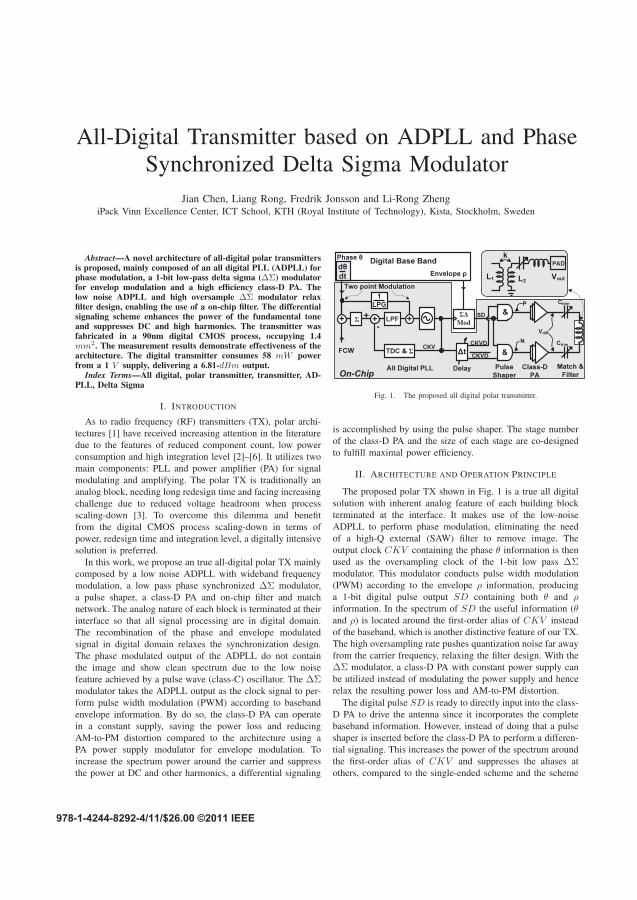
All-Digital Transmitter based on ADPLL and PhaseSynchronized Delta Sigma Modulator
Jian Chen, Liang Rong, Fredrik Jonsson and Li-Rong ZhengiPack Vinn Excellence Center, ICT School, KTH (Royal Institute of Technology), Kista, Stockholm, Sweden
Abstract—A novel architecture of all-digital polar transmittersis proposed, mainly composed of an all digital PLL (ADPLL) forphase modulation, a 1-bit low-pass delta sigma (ΔΣ) modulatorfor envelop modulation and a high efficiency class-D PA. Thelow noise ADPLL and high oversample ΔΣ modulator relaxfilter design, enabling the use of a on-chip filter. The differentialsignaling scheme enhances the power of the fundamental toneand suppresses DC and high harmonics. The transmitter wasfabricated in a 90nm digital CMOS process, occupying 1.4mm
2. The measurement results demonstrate effectiveness of thearchitecture. The digital transmitter consumes 58 mW powerfrom a 1 V supply, delivering a 6.81-dBm output.
Index Terms—All digital, polar transmitter, transmitter, AD-PLL, Delta Sigma
I. INTRODUCTION
As to radio frequency (RF) transmitters (TX), polar archi-tectures [1] have received increasing attention in the literaturedue to the features of reduced component count, low powerconsumption and high integration level [2]–[6]. It utilizes twomain components: PLL and power amplifier (PA) for signalmodulating and amplifying. The polar TX is traditionally ananalog block, needing long redesign time and facing increasingchallenge due to reduced voltage headroom when processscaling-down [3]. To overcome this dilemma and benefitfrom the digital CMOS process scaling-down in terms ofpower, redesign time and integration level, a digitally intensivesolution is preferred.
In this work, we propose an true all-digital polar TX mainlycomposed by a low noise ADPLL with wideband frequencymodulation, a low pass phase synchronized ΔΣ modulator,a pulse shaper, a class-D PA and on-chip filter and matchnetwork. The analog nature of each block is terminated at theirinterface so that all signal processing are in digital domain.The recombination of the phase and envelope modulatedsignal in digital domain relaxes the synchronization design.The phase modulated output of the ADPLL do not containthe image and show clean spectrum due to the low noisefeature achieved by a pulse wave (class-C) oscillator. The ΔΣmodulator takes the ADPLL output as the clock signal to per-form pulse width modulation (PWM) according to basebandenvelope information. By do so, the class-D PA can operatein a constant supply, saving the power loss and reducingAM-to-PM distortion compared to the architecture using aPA power supply modulator for envelope modulation. Toincrease the spectrum power around the carrier and suppressthe power at DC and other harmonics, a differential signaling
1
LPG
+ Σ
TDC & Σ
LPF
FCW
Two point Modulation
ΣΔ
Mod
SD+
-
Digital Base Band
Δt
&+ +
PAD
Vout
&
dθ
dt Envelope ρ
Phase θ
P
NCKVD
CKVD
Vdiff
CKV
All Digital PLL Delay Pulse
Shaper
Class-D
PA
Match &
Filter
Ctrim
Ctrim
On-Chip
k
L1 L2
Fig. 1. The proposed all digital polar transmitter.
is accomplished by using the pulse shaper. The stage numberof the class-D PA and the size of each stage are co-designedto fulfill maximal power efficiency.
II. ARCHITECTURE AND OPERATION PRINCIPLE
The proposed polar TX shown in Fig. 1 is a true all digitalsolution with inherent analog feature of each building blockterminated at the interface. It makes use of the low-noiseADPLL to perform phase modulation, eliminating the needof a high-Q external (SAW) filter to remove image. Theoutput clock CKV containing the phase θ information is thenused as the oversampling clock of the 1-bit low pass ΔΣmodulator. This modulator conducts pulse width modulation(PWM) according to the envelope ρ information, producinga 1-bit digital pulse output SD containing both θ and ρinformation. In the spectrum of SD the useful information (θand ρ) is located around the first-order alias of CKV insteadof the baseband, which is another distinctive feature of our TX.The high oversampling rate pushes quantization noise far awayfrom the carrier frequency, relaxing the filter design. With theΔΣ modulator, a class-D PA with constant power supply canbe utilized instead of modulating the power supply and hencerelax the resulting power loss and AM-to-PM distortion.
The digital pulse SD is ready to directly input into the class-D PA to drive the antenna since it incorporates the completebaseband information. However, instead of doing that a pulseshaper is inserted before the class-D PA to perform a differen-tial signaling. This increases the power of the spectrum aroundthe first-order alias of CKV and suppresses the aliases atothers, compared to the single-ended scheme and the scheme
978-1-4244-8292-4/11/$26.00 ©2011 IEEE
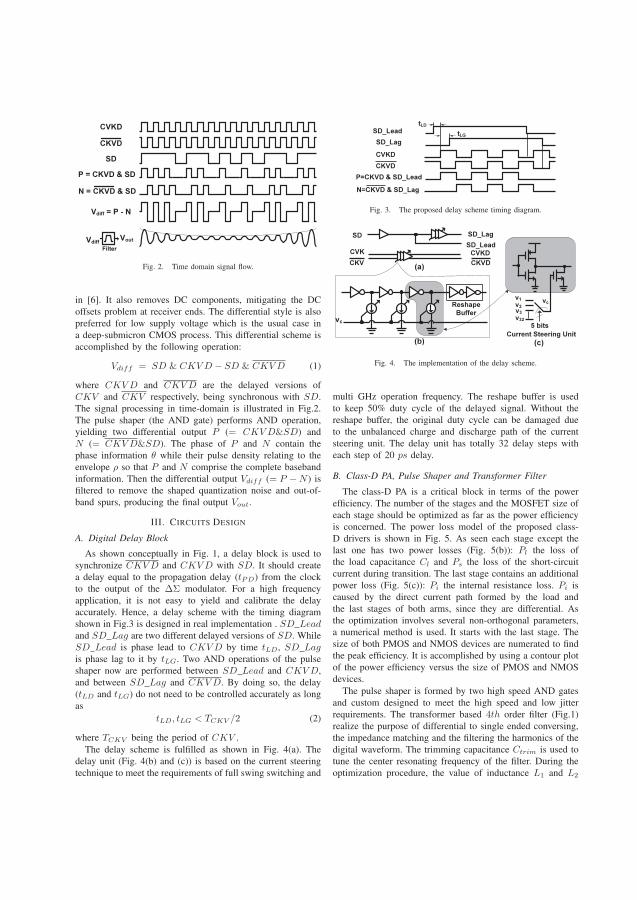
CKVD
SD
P = CKVD & SD
Vdiff = P - N
N = CKVD & SD
Filter
Vdiff
CVKD
Vout
Fig. 2. Time domain signal flow.
in [6]. It also removes DC components, mitigating the DCoffsets problem at receiver ends. The differential style is alsopreferred for low supply voltage which is the usual case ina deep-submicron CMOS process. This differential scheme isaccomplished by the following operation:
Vdiff = SD & CKVD − SD & CKVD (1)
where CKVD and CKVD are the delayed versions ofCKV and CKV respectively, being synchronous with SD.The signal processing in time-domain is illustrated in Fig.2.The pulse shaper (the AND gate) performs AND operation,yielding two differential output P (= CKVD&SD) andN (= CKVD&SD). The phase of P and N contain thephase information θ while their pulse density relating to theenvelope ρ so that P and N comprise the complete basebandinformation. Then the differential output Vdiff (= P −N ) isfiltered to remove the shaped quantization noise and out-of-band spurs, producing the final output Vout.
III. CIRCUITS DESIGN
A. Digital Delay Block
As shown conceptually in Fig. 1, a delay block is used tosynchronize CKVD and CKVD with SD. It should createa delay equal to the propagation delay (tPD) from the clockto the output of the ΔΣ modulator. For a high frequencyapplication, it is not easy to yield and calibrate the delayaccurately. Hence, a delay scheme with the timing diagramshown in Fig.3 is designed in real implementation . SD Leadand SD Lag are two different delayed versions of SD. WhileSD Lead is phase lead to CKVD by time tLD, SD Lagis phase lag to it by tLG. Two AND operations of the pulseshaper now are performed between SD Lead and CKVD,and between SD Lag and CKVD. By doing so, the delay(tLD and tLG) do not need to be controlled accurately as longas
tLD, tLG < TCKV /2 (2)
where TCKV being the period of CKV .The delay scheme is fulfilled as shown in Fig. 4(a). The
delay unit (Fig. 4(b) and (c)) is based on the current steeringtechnique to meet the requirements of full swing switching and
SD_Lead
SD_Lag
CKVD
CVKD
P=CKVD & SD_Lead
N=CKVD & SD_Lag
tLD
tLG
Fig. 3. The proposed delay scheme timing diagram.
v1
v2
v32
v3
5 bits
vc
vc
Reshape
Buffer
Current Steering Unit
CVK
CKV
SD
SD_Lead
SD_Lag
CVKD
CKVD(a)
(b) (c)
Fig. 4. The implementation of the delay scheme.
multi GHz operation frequency. The reshape buffer is usedto keep 50% duty cycle of the delayed signal. Without thereshape buffer, the original duty cycle can be damaged dueto the unbalanced charge and discharge path of the currentsteering unit. The delay unit has totally 32 delay steps witheach step of 20 ps delay.
B. Class-D PA, Pulse Shaper and Transformer Filter
The class-D PA is a critical block in terms of the powerefficiency. The number of the stages and the MOSFET size ofeach stage should be optimized as far as the power efficiencyis concerned. The power loss model of the proposed class-D drivers is shown in Fig. 5. As seen each stage except thelast one has two power losses (Fig. 5(b)): Pl the loss ofthe load capacitance Cl and Ps the loss of the short-circuitcurrent during transition. The last stage contains an additionalpower loss (Fig. 5(c)): Pi the internal resistance loss. Pi iscaused by the direct current path formed by the load andthe last stages of both arms, since they are differential. Asthe optimization involves several non-orthogonal parameters,a numerical method is used. It starts with the last stage. Thesize of both PMOS and NMOS devices are numerated to findthe peak efficiency. It is accomplished by using a contour plotof the power efficiency versus the size of PMOS and NMOSdevices.
The pulse shaper is formed by two high speed AND gatesand custom designed to meet the high speed and low jitterrequirements. The transformer based 4th order filter (Fig.1)realize the purpose of differential to single ended conversing,the impedance matching and the filtering the harmonics of thedigital waveform. The trimming capacitance Ctrim is used totune the center resonating frequency of the filter. During theoptimization procedure, the value of inductance L1 and L2
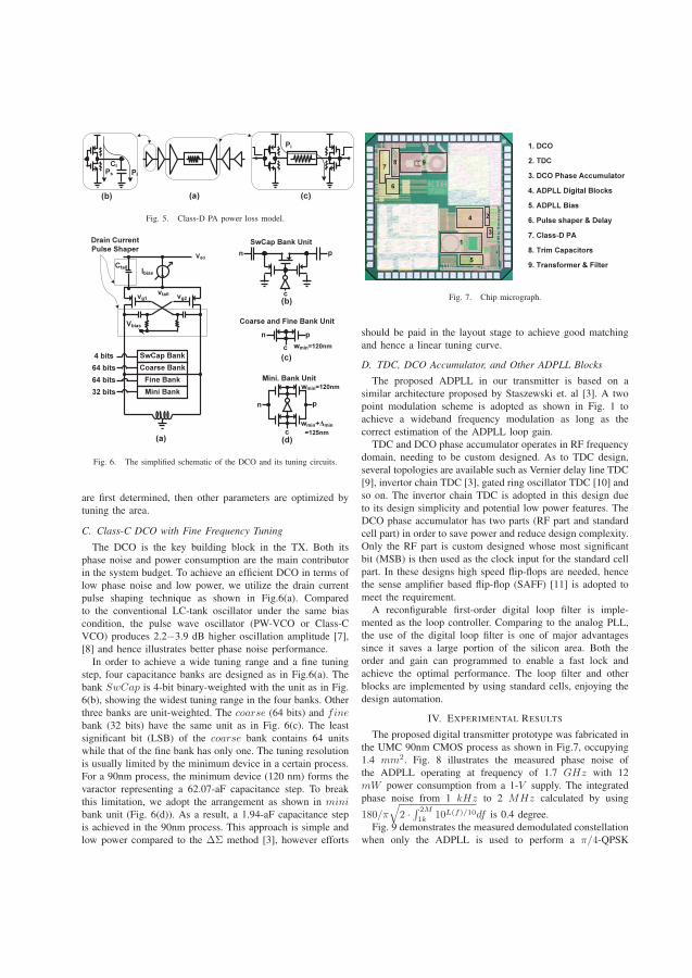
Pl
Cl
Ps
Pi
(c)(a)(b)
Fig. 5. Class-D PA power loss model.
Ctail
Vbias
Ibias
Vdd
vtail
SwCap Bank
Coarse Bank
Fine Bank
Mini Bank
Drain Current
Pulse Shaper
4 bits
64 bits
64 bits
32 bits
(a)
vg1 vg2
Coarse and Fine Bank Unit
n p
c(b)
n p
c
n p
cwmin+Δmin
=125nm
wmin=120nm
wmin=120nm
(c)
(d)
SwCap Bank Unit
Mini. Bank Unit
Fig. 6. The simplified schematic of the DCO and its tuning circuits.
are first determined, then other parameters are optimized bytuning the area.
C. Class-C DCO with Fine Frequency Tuning
The DCO is the key building block in the TX. Both itsphase noise and power consumption are the main contributorin the system budget. To achieve an efficient DCO in terms oflow phase noise and low power, we utilize the drain currentpulse shaping technique as shown in Fig.6(a). Comparedto the conventional LC-tank oscillator under the same biascondition, the pulse wave oscillator (PW-VCO or Class-CVCO) produces 2.2−3.9 dB higher oscillation amplitude [7],[8] and hence illustrates better phase noise performance.
In order to achieve a wide tuning range and a fine tuningstep, four capacitance banks are designed as in Fig.6(a). Thebank SwCap is 4-bit binary-weighted with the unit as in Fig.6(b), showing the widest tuning range in the four banks. Otherthree banks are unit-weighted. The coarse (64 bits) and finebank (32 bits) have the same unit as in Fig. 6(c). The leastsignificant bit (LSB) of the coarse bank contains 64 unitswhile that of the fine bank has only one. The tuning resolutionis usually limited by the minimum device in a certain process.For a 90nm process, the minimum device (120 nm) forms thevaractor representing a 62.07-aF capacitance step. To breakthis limitation, we adopt the arrangement as shown in minibank unit (Fig. 6(d)). As a result, a 1.94-aF capacitance stepis achieved in the 90nm process. This approach is simple andlow power compared to the ΔΣ method [3], however efforts
7
1. DCO
2. TDC
3. DCO Phase Accumulator
4. ADPLL Digital Blocks
5. ADPLL Bias
6. Pulse shaper & Delay
7. Class-D PA
8. Trim Capacitors
9. Transformer & Filter
1
2
3
5
4
98
6
Fig. 7. Chip micrograph.
should be paid in the layout stage to achieve good matchingand hence a linear tuning curve.
D. TDC, DCO Accumulator, and Other ADPLL Blocks
The proposed ADPLL in our transmitter is based on asimilar architecture proposed by Staszewski et. al [3]. A twopoint modulation scheme is adopted as shown in Fig. 1 toachieve a wideband frequency modulation as long as thecorrect estimation of the ADPLL loop gain.
TDC and DCO phase accumulator operates in RF frequencydomain, needing to be custom designed. As to TDC design,several topologies are available such as Vernier delay line TDC[9], invertor chain TDC [3], gated ring oscillator TDC [10] andso on. The invertor chain TDC is adopted in this design dueto its design simplicity and potential low power features. TheDCO phase accumulator has two parts (RF part and standardcell part) in order to save power and reduce design complexity.Only the RF part is custom designed whose most significantbit (MSB) is then used as the clock input for the standard cellpart. In these designs high speed flip-flops are needed, hencethe sense amplifier based flip-flop (SAFF) [11] is adopted tomeet the requirement.
A reconfigurable first-order digital loop filter is imple-mented as the loop controller. Comparing to the analog PLL,the use of the digital loop filter is one of major advantagessince it saves a large portion of the silicon area. Both theorder and gain can programmed to enable a fast lock andachieve the optimal performance. The loop filter and otherblocks are implemented by using standard cells, enjoying thedesign automation.
IV. EXPERIMENTAL RESULTS
The proposed digital transmitter prototype was fabricated inthe UMC 90nm CMOS process as shown in Fig.7, occupying1.4 mm2. Fig. 8 illustrates the measured phase noise ofthe ADPLL operating at frequency of 1.7 GHz with 12mW power consumption from a 1-V supply. The integratedphase noise from 1 kHz to 2 MHz calculated by using
180/π√
2 ·∫ 2M
1k10L(f)/10df is 0.4 degree.
Fig. 9 demonstrates the measured demodulated constellationwhen only the ADPLL is used to perform a π/4-QPSK
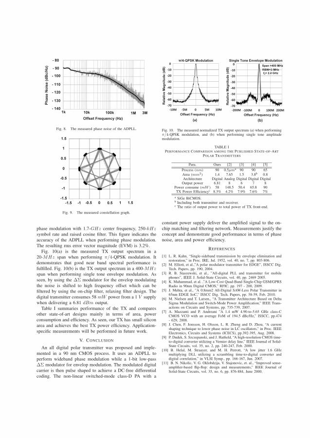
- 80
- 100
- 120
- 1401k 10k 100k 1M 3M
Ph
as
e N
ois
e (
dB
c/H
z)
Offset Frequency (Hz)
- 90
- 110
- 130
Fig. 8. The measured phase noise of the ADPLL.
1.5
1
0.5
0
-0.5
-1
-1.5
-1.5 -1 -0.5 0 0.5 1 1.5
Fig. 9. The measured constellation graph.
phase modulation with 1.7-GHz center frequency, 250-kHzsymbol rate and raised cosine filter. This figure indicates theaccuracy of the ADPLL when performing phase modulation.The resulting rms error vector magnitude (EVM) is 3.2%.
Fig. 10(a) is the measured TX output spectrum in a20-MHz span when performing π/4-QPSK modulation. Itdemonstrates that good near band spectral performance isfulfilled. Fig. 10(b) is the TX output spectrum in a 400-MHzspan when performing single tone envelope modulation. Asseen, by using the ΔΣ modulator for the envelop modulatingthe noise is shifted to high frequency offset which can befiltered by using the on-chip filter, relaxing filter design. Thedigital transmitter consumes 58 mW power from a 1 V supplywhen delivering a 6.81 dBm output.
Table I summaries performance of the TX and comparesother state-of-art designs mainly in terms of area, powerconsumption and efficiency. As seen, our TX has small siliconarea and achieves the best TX power efficiency. Application-specific measurements will be performed in future work.
V. CONCLUSION
An all digital polar transmitter was proposed and imple-mented in a 90 nm CMOS process. It uses an ADPLL toperform wideband phase modulation while a 1-bit low-passΔΣ modulator for envelop modulation. The modulated digitalcarrier is then pulse shaped to achieve a DC-free differentialcoding. The non-linear switched-mode class-D PA with a
(a)
Span =20 MHz
‐70
‐60
‐50
‐40
‐30
‐20
‐10
0
‐10M ‐5M 0 5M 10M
Offset Frequency (Hz)
Rela
tive M
ag
nit
ud
e (
dB
)
π/4-QPSK Modulation
(b)
‐200M ‐100M 0 100M 200M
‐70
‐60
‐50
‐40
‐30
‐20
‐10
0
Offset Frequency (Hz)
Rela
tive M
ag
nit
ud
e (
dB
)
RBW=3 MHz
Single Tone Envelope Modulation
Span =400 MHz
fo= 2.4 GHz
Fig. 10. The measured normalized TX output spectrum (a) when performingπ/4-QPSK modulation, and (b) when performing single tone amplitudemodulation.
TABLE IPERFORMANCE COMPARISON AMONG THE PUBLISHED STATE-OF-ART
POLAR TRANSMITTERS
Para. Ours [2] [3] [4] [5]
Process (nm) 90 0.5μma 90 90 65Area (mm2) 1.4 7.65 1.5 3.8b 0.8Architecture Digital Analog Digital Digital Digital
Output power 6.81 8 6 7 8Power consume (mW ) 58 148.5 50.4 65.8 90TX Power Efficiencyc 8.3% 4.2% 7.9% 7.6% 7%
a SiGe BiCMOS.b Including both transmitter and receiver.c The ratio of output power to total power of TX front-end.
constant power supply deliver the amplified signal to the on-chip matching and filtering network. Measurements justify theconcept and demonstrate good performance in terms of phasenoise, area and power efficiency.
REFERENCES
[1] L. R. Kahn, “Single-sideband transmission by envelope elimination andrestoration,” in Proc. IRE, Jul. 1952, vol. 40, no. 7, pp. 803-806.
[2] M. Elliott, et al.,”A polar modulator transmitter for EDGE”, ISSCC Dig.Tech. Papers, pp. 190, 2004.
[3] R. B. Staszewski, et al., ”All-digital PLL and transmitter for mobilephones”, IEEE J. Solid-State Circuits, vol. 40, pp. 2469 2005.
[4] K. Muhammad, et al. ,”A Low-Cost Quad-Band Single-Chip GSM/GPRSRadio in 90nm Digital CMOS,” RFIC, pp. 197 - 200, 2009.
[5] J. Mehta, et al., ”A 0.8mm2 All-Digital SAW-Less Polar Transmitter in65nm EDGE SoC,” ISSCC Dig. Tech. Papers, pp. 58-59, Feb. 2010.
[6] M. Nielsen and T. Larsen,, “A Transmitter Architecture Based on DeltaSigma Modulation and Switch-Mode Power Amplification,” IEEE Trans-actions on Circuits and Systems, pp. 735-739, 2007.
[7] A. Mazzanti and P. Andreani ”A 1.4 mW 4.90-to-5.65 GHz class-CCMOS VCO with an average FoM of 194.5 dBc/Hz,” ISSCC, pp.474- 629, 2008.
[8] J. Chen, F. Jonsson, H. Olsson, L. R. Zheng and D. Zhou, “A currentshaping technique to lower phase noise in LC oscillators,” in Proc. IEEEElectronics, Circuits and Systems (ICECS), pp.392-395, Aug. 2008.
[9] P. Dudek, S. Szczepanski, and J. Hatfield, “A high-resolution CMOS time-to-digital converter utilizing a Vernier delay line,” IEEE Journal of Solid-State Circuits, vol. 35, no. 2, pp. 240-247, Feb. 2000.
[10] B. Helal, M. Straayer, and M. H. Perrott, “A low jitter 1.6 GHzmultiplying DLL utilizing a scrambling time-to-digital converter anddigital correlation,” in VLSI Symp., pp. 166-167, Jun. 2007.
[11] B. N. Nikolic, V. G. Oklobdzija, V. Stajonovic, et. al., “Improved sense-amplifier-based flip-flop: design and measurements,” IEEE Journal ofSolid-State Circuits, vol. 35, no. 6, pp. 876-884, June 2000.

PAPER 6
A 11.4dBm 90nm CMOS H-Bridge ResonatingPolar Amplifier using RF Sigma Delta Modulation
1Liang Rong, 1Fredrik Jonsson, 1,2Li-Rong Zheng1iPack Center, School of ICT, Royal Institute of Technology (KTH), Stockholm, Sweden
2State Key Lab of ASICs and Systems, ICT School, Fudan University, Shanghai, P.R. China
Email: {liangr, fjon, lirong}@kth.se
Abstract—Using RF Sigma Delta Modulation (RFSDM), aclass-D polar amplifier in H-Bridge configuration can work in res-onating mode and minimize the switching loss for high efficiencypolar transmitters. The high oversampling ratio envelop bitstream created by the low pass RFSDM is phase modulated anddigitally mixed with quantized RF carrier to give a modulatedRF digital signal. By taking the advantage of high speed andaccurate digital CMOS process, this ’information combination’architecture can achieve high efficiency and reduce the need forexternal filter components. A polar power amplifier based on thisconcept is implemented in 90nm CMOS process and achieved apeak output power of 11.4dBm with 19.3% efficiency at 1.0Vpower supply. The total area is 0.72mm2 including an on-chipfilter matching network designed for 2.4GHz to 2.7GHz band.
Index Terms—Low Pass RF Sigma Delta Modulation, H-BridgeDigital Polar Amplifier, on-Chip Filter Matching Network, DigitalDelay Trimming.
I. INTRODUCTION
Polar transmitter has been proved to give high efficiency in
constant envelop [1] and varying envelop wireless communica-
tions [2][3]. For systems with high linearity and large signal-
to-noise ratio (SNR) requirements, the use of linear power
amplifier (PA) incurs large power waste and placed a severe
constraint on the whole system efficiency. While for polar
transmitter, by using switching power amplifiers like class D
or E working in saturation mode, a theoretical 100% efficiency
can be achieved [4].
In large peak-to-average ratio (PAR) signal case [5], practi-
cal polar amplifier will experience substantial power modula-
tion loss due to the Rayleigh distribution of envelop amplitude.
To improve the efficiency of power modulator in traditional
polar architecture (Fig. 1), the varying envelop signal is
used as reference to generate pulse width modulated (PWM)
power supply to the amplifier [6][7]. This topology requires
large off-chip filtering components and the optimization of
filter bandwidth is a compromise between envelop linearity
and efficiency[8]. In traditional polar amplifier, the AM-
PM distortion is another problem and compensation or pre-
distortion algorithms have to be used to shape adjacent channel
noise [12]. Other schemes [1][3] using band pass delta-sigma
modulation (BPDSM) and class-D PA have been proposed.
These schemes require sampling clock higher than carrier
frequency and can be very difficult to implement for over
giga-Hertz band transmissions. And it has varying switching
position when output current is large, the switching loss will
Polar Transmitter
PLL
PowerModulator
Class E
Envelop
PolarBasebandModulator
DSP
)()( 22 tQtI �
),( ��f
off-chipLC filter
BandpassFilter
Fig. 1. Power (envelope) modulation scheme polar transmitter.
FPGA
Envelop
Power
H-BridgeClass D
Delay Trimming Control
A(t)SD a
b
Θ(t)ADPLL
Out+Vdiff-
AND
LP Sigma DeltaModulator
TDC & Σ
PolarBasebandModulator
clkp
off-chipon-chip
Pulse Shaping& Driverclkn
Filter Matching Network
k
L1
2Ci
L2SD
Lo
Co
Fig. 2. H-Bridge resonating polar amplifier topology.
be high for BPDSM. Alternative scheme employing low-pass
delta sigma modulation [4] has been proposed but it generates
maximum output power at low frequency band.
In this work, alternative to ’power combination’ scheme,
an ’information combination’ architecture is demonstrated in
Fig. 2. Using low-pass RF sigma delta modulation clocked at
carrier frequency, an envelop bit stream signal is generated. By
combining the RFSDM bit stream with RF carrier, H-bridge
configuration class-D amplifier fully utilize the low supply
voltage and the zero crossing switching ensured minimum
switching loss. Except for the analog interface, matching
network and driver stages, the system can take the advantage
of fast and accurate digital CMOS process and these features
are attractive in future wireless communication transmitter
systems with scaled CMOS process.
The content of this work is arranged in following orders. In
Section II, proposed polar amplifier architecture is analyzed
from both transient and spectral domains. The circuit designs
are presented in section III and measurement results will be
presented and explained in section IV. The last part will be
the conclusions on the proposed transmitter architecture and
further works.
978-1-4577-0704-9/10/$26.00 ©2011 IEEE 307
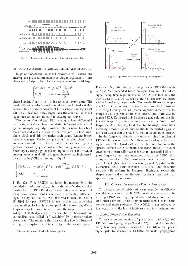
a=SD & clkp
clkp
SD
Vdiff = a-b
Out
Envelop
b=SD & clkn
Bandpass Filter
Vdiff
GND
Fig. 3. Transient signal processing illustration in polar PA.
II. POLAR ALGORITHM AND AMPLIFIER ARCHITECTURE
In polar transmitter, baseband processor will extract the
envelop and phase information according to Equation (1). The
phase control signal Θ(t) has to be processed to avoid large
⎧⎨⎩Env(t) =
√I(t)2 +Q(t)2
Θ(t) = arctan(Q(t)
I(t)
) (1)
phase hopping from -π to +π due to its complex nature. The
bandwidth of envelop signal should also be limited suitably
because the effective bandwidth of the baseband envelop signal
will be at least two times larger than the complex baseband
signal due to the discontinuity in envelop derivative.
The output from digital PLL is a quantized differential
carrier signal and the phase modulation information is defined
by the rising/falling edge position. The positive branch of
the differential clock is used as the low pass RFSDM mod-
ulator clock and this distinctive architecture feature brings
three advantages. Firstly, the phase and envelop signal path
are synchronized, this helps to reduce the spectral regrowth
problem caused by phase and envelop timing mismatch [9].
Secondly, by using high oversampling ratio, the 1-bit RFSDM
envelop output signal will have good linearity and high signal-
to-noise ratio (SNR) according to Eq. (2).1
⎧⎪⎪⎨⎪⎪⎩SNRmax = 10lg(
3
222N ) + 10lg(
2k + 1
π2kOSR2k+1)
OSR =fc
2 ·Bmax
(2)
In Eq. (2), N is RFSDM resolution bit number, k is the
modulation order and Bmax is maximum effective envelop
bandwidth. The RFSDM shaped quantization noise is pushed
away from carrier center and ease the on-chip filter de-
sign. Thirdly, not like BPDSM or PWM modulation used in
[1][3][6], low pass RFSDM do not need to use extra high
oversampling clock so it is more preferable in over giga-Hertz
frequency applications. What is more, the output current and
voltage of H-Bridge class-D PA will be in phase and this
can realize the so called ’soft switching’ PA to further reduce
power loss. The transient signal processing flow is illustrated
in Fig. 3 to explain the critical nodes in the polar amplifier.
1This is a single tone SDM calculation equation.
f
SD
RFSDMenvelop bit stream
f
clk
fc 3fc 5fc
Quantized CarrierSquare Wave
Vdiff
fc 3fc 5fc
Mixed Signal
B
BandpassFilter
Out
fc 3fc 5fc
Filtered SignalBandpass Filter
fc 2fc
f f
Fig. 4. Spectrum analysis of polar power amplifier.
For every clkp pulse, there are timing matched RFSDM signals
SD and SD′ generated based on input Envelop. To reduce
signal setup time requirements in ’AND’ standard cell, the
SD′ signal is 1/2Tclk lagged behind SD and they are mixed
with clkp and clkn respectively. The pseudo differential output
a and b are input to pulse shaping driver stage (PSDS) instead
of driving H-bridge class-D power amplifier directly, the H-
bridge class-D power amplifier is source pull optimized by
tuning PSDS. Compared to [4]’s single ended solution, the dif-
ferential output Vdiff concentrates more power at fundamental
frequency. After filtering by differential to single ended filter
matching network, phase and amplitude modulated signal is
reconstructed at output node Out with high coding efficiency.
In the frequency domain, the transient signal mixing of
RFSDM bit stream SD (2nd Quadrant) and quantized clksquare wave (1st Quadrant) will be the convolution in the
spectral domain (3rd Quadrant). The shaped noise of RFSDM
envelop bit stream will have rising amplitude until half sam-
pling frequency and then attenuated due to the SINC mask
of square waveform. The quantization noise between 0 and
fc will be higher than the noise in fc and 2fc due to the
overlapped noise from negative axle. The filter matching
network will perform the bandpass filtering to reduce the
shaped noise and ensure the Out spectrum compliant with
spectral mask requirements.
III. CIRCUIT DESIGN FOR POLAR AMPLIFIER
To increase the adaptivity of polar amplifier in different
modulation schemes, the RFSDM modulator is realized by
off-chip FPGA with high speed serial interface and the on-
chip blocks are mostly re-using standard digital cells in the
control and mixing circuits. The ADPLL is not included in
this work due to the layout limitations and test configuration.
A. Digital Phase Delay Trimming
To ensure correct mixing of phase (clkp and clkn) and
RFSDM envelop signal (SD and SD′), a digital controlled
delay trimming circuit is inserted in the differential phase
signal path to balance the RFSDM modulator propagation
308
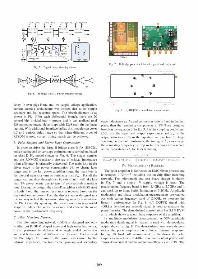
Delay Unit 1
P[0::4]
Delay Unit 2 Delay Unit 3 Delay Unit 4
clkp
clkn
B[0::4]
Iref
Duty CycleRestorationBuffer
A[0::4] X1X2X4X8X16
Positive Phase Part
Negative PhasePart
A[0::4]
N[0::4] P[0::4]
B[5::9]A[5::9]
N[0::4] P[0::4]
B[10::14]A[10::14]
N[0::4] P[0::4]
B[14::19]A[14::19]
N[0::4]
B[0::4]
Fig. 5. Digital delay trimming circuit.
Ps
LoadPl1
Cg1
Pint ronron
Pl2
Cg2n
Fig. 6. H-bridge class-D power amplifier model.
delay. In over giga-Hertz and low supply voltage application,
current steering architecture was chosen due to its simple
structure and fast response speed. The circuit diagram is as
shown in Fig. 5.For each differential branch, there are 20
control bits divided into 4 groups and it can realized total
128 monotone integer delay steps with 12pS each (in the linear
region). With additional interface buffer, this module can cover
0.5 to 3 periods delay range so that when different order of
RFSDM is used, correct timing match can be achieved.
B. Pulse Shaping and Driver Stage Optimization
In order to drive the large H-bridge class-D PA (HBCD),
pulse shaping and driver stage optimization is carried out based
on class-D PA model shown in Fig. 6. The stages number
and the P/NMOS transistors size are of critical importance
when efficiency is primarily concerned. The main loss in the
driver stage is the power consumption Plx to charge later
stages and in the last power amplifier stage, the main loss is
the internal transistor turn on resistance loss Pint. For all the
stages, current short through loss Ps exists but it will take less
than 1% power waste due to tens of pico-seconds transition
time. During the design, the class-D amplifier (P/NMOS size)
is firstly fixed, the turn on resistance is reduced based on the
requested output power. Then the driver stage is designed in a
reverse way to find the optimized driving waveform input into
the PA. Generally speaking, the waveform is in trapezoidal
shape to reduce 3rd order harmonics and concentrate more
power at the fundamental frequency.
C. Filter Matching Network
The filter matching network (FMN) is designed not only
to filter out RFSDM shaped noise and high order harmonics,
it also performs the differential to single ended conversion
and match the external 50Ohm load to small load seen at
the PA output. To minimize the power loss caused by the
intrinsic impedance, the transformer primary and secondary
Filter Match Network
Class-D PA
Control Interface
Delay Trimm
SAFF
980um
980u
m
Fig. 7. H-Bridge polar amplifier micrograph and test board.
Ref Lvl
0 dB 0 dBm
Ref Lvl
0 dB 0 dBm
IFOVLD CF 2.44400311 GHz
SR 400 kHz
Symbol/Errors
Demod �/4 DQPSK
UNCAL
Ref Lvl
0 dB 0 dBm
Ref Lvl
0 dB 0 dBm
A
CF 2.44400311 GHz
00SR 400 kHz
Meas Signal
iConstellation
/Demod �/4 DQPSK
IMAG
T1
IFOVLDUNCAL
-1
1
Marker 1 [T2] 0 sym
Value 3
Fig. 8. π/4DQPSK constellation measurements.
stage inductance L1 L2 and conversion ratio is fixed in the first
place, then the remaining components in FMN are designed
based on the equation 3. In Eq. 3, k is the coupling coefficient.
CiCo are the input and output capacitance and Lo is the
output inductance. From the equation we can find for large
coupling coefficient transformer, the tuning of Ci can change
the resonating frequency, so top metal openings are reserved
on the capacitance Ci for laser trimming.
MCinCoS3Rl
CoL2S2[(1 − k2)L1CiS2 + 1
]+ (L1CiS2 + 1)(LoCoS2 + RlCoS + 1)
(3)
IV. MEASUREMENT RESULTS
The polar amplifier is fabricated in UMC 90nm process and
it occupies 0.72mm2 including the on-chip filter matching
network. The micrograph and test board design is shown
in Fig. 7 and a single 1V supply voltage is used. The
measurement freqency band is from 2.4GHz to 2.7GHz and it
can work up to input buffer limitation of 3.2GHz. Amplitude
modulation and phase modulation measurements are carried
out with carrier frquency band of 2.4GHz to measure the
linearity performance. In Fig. 8, π/4 DQPSK signal with
400kSps (symbol per second) signal is used to measure the
phase linearity. The demodulated constellation has 8.1% EVM
error which shows a good phase response of the amplifier.
In amplitude modulation measurement, A 60% amplitude
modulation depth signal bit stream is used with demodulated
output shown in Fig. 9. The demodulated sine wave demon-
strates the polar amplifier has a linear dynamic response.
In Fig. 10, load pull measurement results shows the polar
amplifier can achieve 11.4dBm maximum output power with
72mA drain current and the maximum efficiency is 19.3%. The
309
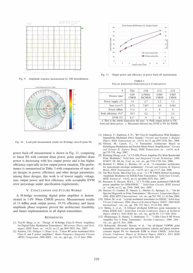
Ref Lvl
0 dB 0 dBm
Ref Lvl
0 dB 0 dBm
CF 2.46000392 GHz
DEMOD BW: 500 kHz
Real Time OFF
AF-Signal
AM [%]
A
START 0 s STOP 200 �s
-80
-60
-40
-20
0
20
40
60
80
-100
100
Date: 11.SEP.2010 21:16:19
Fig. 9. Amplitude response measurement by AM demodulation.
0.1
0.2
0.3
0.4
0.5
0.6
0.7
0.8
0.9
1.0
1.2
1.4
1.6
1.8
2.0
3.0
4.0
5.0
10 20 30 40 50
0.1
0.1
0.2
0.2
0.2
0.2
0.3
0.3
0.4
0.4
0.4
0.4
0.5
0.5
0.6
0.6
0.6
0.6
0.7
0.7
0.8
0.8
0.8
0.8
0.9
0.9
1.0
1.0
1.0
1.0
1.2
1.2
1.4
1.4
1.6
1.6
1.8
1.8
2.0
2.0
3.0
3.0
4.0
4.0
5.0
5.0
10
10
20
20
30
30
40
40
50
50
0.00
0.01
0.02
0.03
0.04
0.05
0.06
0.070.08 0.09 0.10 0.11 0.12 0.13 0.14 0.15 0.16 0.17 0.18
0.190.20
0.210.22
0.230.24
0.250.26
0.270.28
0.290.30
0.31
0.320.330.340.350.360.370.380.390.400.410.420.43
0.44
0.45
0.46
0.47
0.48
0.49
Load Pull Measurement (Pmax=11.4dBm)
8
8.5
9
9.5
10
10.5
11
11.5
12
Fig. 10. Load pull measurement results for H-bridge class-D polar PA.
power back-off measurement is shown in Fig. 11, comparing
to linear PA with constant drain power, polar amplifier drain
power is decreasing with less output power and it has higher
efficiency especially in low output power situation. The perfor-
mance is summarized in Table. I with comparisons of state-of-
art designs in power, efficiency and other design parameters,
among these designs, this work is of lowest supply voltage,
max output power and best efficiency with acceptable EVM
error percentage under specification requirements.
V. CONCLUSIONS AND FUTURE WORKS
A H-bridge resonating digital polar amplifier is demon-
strated in 1.0V 90nm CMOS process. Measurement results
of 11.4dBm peak output power, 19.3% efficiency and linear
amplitude phase response proved the architecture feasibility
and future implementation in all digital transmitters.
REFERENCES
[1] Tsai-Pi Hung; et al., ”Design of H-Bridge Class-D Power Amplifiersfor Digital Pulse Modulation Transmitters,” Microwave Theory and Tech-niques, IEEE Trans. on , vol.55, no.12, pp.2845-2855, Dec. 2007.
[2] Kitchen, J.D.; Deligoz, I.; Kiaei, et al., ”Linear RF polar modulated SiGeClass E and F power amplifiers,” Radio Frequency Integrated Circuits(RFIC) Symposium, 2006 IEEE , vol., no., pp.4 pp., 11-13 June 2006.
Drain�Power�&�Efficiency�V.S.�Output�Power
0
10
20
30
40
50
60
70
80
1 3 5 7 9 11 13 15Output�Power�(mW)
Drain�Po
wer�(m
W)
0
3
6
9
12
15
18
21
24
Efficiency�(%
)
Drain�Power(mW)
EfficiencyNorm(%)
Fig. 11. Output power and efficiency in power back-off measurement.
TABLE IPOLAR AMPLIFIER PERFORMANCE COMPARISON
# This [10] [11] [13]
Process (um)0.09
CMOS0.5SiGe
BiCMOS0.065
CMOS0.065
CMOS
Power supply (V) 1.0 2.7 1.2 1.2
Area (mm2) 0.72 7.65a 0.8 0.563
Power (dBm) 11.4 8 8 0
Peak efficiency (%)b 19.3 4.2 7 2.4
EVM (%) 8.1c 9 6 6.1a. This is the whole transceiver die area. b. Peak output power to TX
front-end drain power. c. Maximum allowed rms EVM is 9% for EDGE.
[3] Johnson, T.; Stapleton, S. P.;, ”RF Class-D Amplification With BandpassSigmaDelta Modulator Drive Signals,” Circuits and Systems I: RegularPapers, IEEE Transactions on , vol.53, no.12, pp.2507-2520, Dec. 2006.
[4] Nielsen, M.; Larsen, T.;, ”A Transmitter Architecture Based onDeltaSigma Modulation and Switch-Mode Power Amplification,” Circuitsand Systems II: Express Briefs, IEEE Transactions on , vol.54, no.8,pp.735-739, Aug. 2007.
[5] Renliang Zheng; et al., ”A 5.5-GHz Power Amplifier For Wide BandwidthPolar Modulator,” Solid-State and Integrated Circuit Technology, 2006.ICSICT ’06. 8th Int. Conf. on, vol., no., pp.1724-1726, Oct. 2006.
[6] Berland, C.; Hibon, I.; Bercher, J.F.; et al., ”A transmitter architecturefor nonconstant envelope modulation,” Circuits and Systems II: ExpressBriefs, IEEE Transactions on , vol.53, no.1, pp.13-17, Jan. 2006.
[7] Tae-Woo Kwak; Min-Chul Lee; et al., ”A 2 W CMOS Hybrid SwitchingAmplitude Modulator for EDGE Polar Transmitters,” Solid-State Circuits,IEEE Journal of , vol.42, no.12, pp.2666-2676, Dec. 2007.
[8] Reynaert, P.; Steyaert, M.S.J.;, ”A 1.75-GHz polar modulated CMOS RFpower amplifier for GSM-EDGE,” ” Solid-State Circuits, IEEE Journalof , vol.40, no.12, pp. 2598- 2608, Dec. 2005.
[9] Strasser, G.; Lindner, B.; Maurer, L.; Hueber, G.; Springer, A.; , ”On theSpectral Regrowth in Polar Transmitters,” Microwave Symposium Digest,2006. IEEE MTT-S International , vol., no., pp.781-784, 11-16 June 2006.
[10] Elliott, M.; et al., ”A polar modulator transmitter for EDGE,” Solid-StateCircuits Conference, 2004. Digest of Technical Papers. ISSCC. 2004 IEEEInternational , vol., no., pp. 190- 522 Vol.1, 15-19 Feb. 2004.
[11] Mehta, J.; et al., ”A 0.8mm2 all-digital SAW-less polar transmitter in65nm EDGE SoC,” Solid-State Circuits Conference Digest of TechnicalPapers (ISSCC), 2010 IEEE Int., vol., no., pp.58-59, 7-11 Feb. 2010.
[12] Hietakangas, S.; Rautio, T.; Rahkonen, T.; , ”1 GHz Class E RF PowerAmplifier For A Polar Transmitter,” Norchip Conference, 2006. 24th ,vol., no., pp.5-9, Nov. 2006.
[13] Kobayashi, Hiroyuki; Kousai, et al., ”An all-digital 8-DPSK polartransmitter with second-order approximation scheme and phase rotation-constant digital PA for bluetooth EDR in 65nm CMOS,” Solid-StateCircuits Conference Digest of Technical Papers (ISSCC), 2011 IEEEInternational , vol., no., pp.174-176, 20-24 Feb. 2011
310

PAPER 7
1154 IEEE JOURNAL OF SOLID-STATE CIRCUITS, VOL. 47, NO. 5, MAY 2012
The Design of All-Digital Polar Transmitter Based onADPLL and Phase Synchronized ModulatorJian Chen, Liang Rong, Student Member, IEEE, Fredrik Jonsson, Geng Yang, and Li-Rong Zheng
Abstract—An improved architecture of polar transmitter (TX)is presented. The proposed architecture is digitally-intensive andmainly composed of an all-digital PLL (ADPLL) for phasemodula-tion, a 1-bit low-pass delta sigma modulator for envelop modu-lation, and a H-bridge class-D power ampli er (PA) for differentialsignaling. The modulator is clocked using the phase modulatedRF carrier to ensure phase synchronization between the amplitudeand phase path, and to guarantee the PA is switching at zero cross-ings of the output current.An on-chip pre- lter is used to reduce the parasitic capacitance
from packages at the switch stage output. The high over samplingratio of the modulator move quantization noise far away fromthe carrier frequency, ensuring good in-band performance andrelax lter requirements. The on-chip lter also acts as impedancematching and differential to single-ended conversion.The measured digital transmitter consumes 58 mW from a 1-V
supply at 6.8 dBm output power.
Index Terms—ADPLL, all digital, CMOS, class-C DCO, class-DPA, Delta Sigma, polar transmitter.
I. INTRODUCTION
I N RADIO frequency (RF) transmitter (TX) applications,polar architecture [1] has received increasing attention in
the literature due to its high power ef ciency, reduced compo-nent count and high integration level [2]–[5]. The polar archi-tecture can potentially achieve high power ef ciency since anef cient but nonlinear power ampli er (PA), such as class D orE, can be adopted. This is an advantage in contemporary wire-less standards where the high peak-to-average ratio reduces theef ciency of a linear PA considerably.A challenge in polar architectures is to realize power ef cient
amplitude modulation path. The amplitude modulation does notonly need to be power ef cient, but also synchronized with thephase information. The large signal shifts bias point of the PAcreating amplitude to phase conversion, and also cause a non-linear relation between the amplitude modulation signal and the
Manuscript received September 01, 2011; revised December 09, 2011; ac-cepted December 18, 2011. Date of publication March 19, 2012; date of currentversion April 25, 2012. This paper was approved by Guest Editor Georg Boeck.This work was supported by Vinnova (The Swedish Governmental Agency forInnovation Systems) through the Vinn Excellence Centers Program.J. Chen, L. Rong, F. Jonsson, and G. Yang are with iPack Vinn Excellence
Center, ICT School KTH (Royal Institute of Technology), Kista, Stockholm,Sweden (e-mail: [email protected]).L.-R. Zheng is with iPack Vinn Excellence Center, ICT School KTH (Royal
Institute of Technology), Kista, Stockholm, Sweden. He is also with the StateKey Laboratory of ASICs and Systems, Fudan University, 200433 Shanghai,China.Color versions of one or more of the gures in this paper are available online
at http://ieeexplore.ieee.org.Digital Object Identi er 10.1109/JSSC.2012.2186720
output power. This makes polar modulation transmitters oftenrequire complex pre-distortion and calibration schemes [6].With process scaling-down the pure analog design entails
long redesign time and confronts increasing challenge due toreduced voltage headroom. To overcome the dilemma and thusbene t from the process scaling in terms of power and area orintegration level, the digitally-intensive solution has been pro-posed [7]. Digital schemes using RF pulse width modulation(PWM) [8] and bandpass delta sigma (BPDSM) [9] have beenproposed. These schemes allow the power ampli er to work atconstant supply voltage, but requires switching at frequencieshigher than the RF carrier. The high frequency makes the cir-cuit implementation dif cult. Also since switching not alwaysoccurs at the zero crossing of the output current, switch behaviorwill be amplitude dependent causing linearity problems and re-duced power ef ciency.In this work, the detailed design of the all-digital polar TX
[10] and measurements are presented. Themain signal path con-sists of an ADPLL, a 1-bit low-pass modulator, a pulseshaper and a H-bridge class-D PA. Most signal processing is ac-complished in digital domain, reducing the design complexitywhile increasing the programmability and effectiveness. The
modulator is clocked by the phase modulated carrier andpulse shaped to maximize the power around the carrier fre-quency. This ensures switching of the power ampli er alwaysoccurs in the zero crossing of the output current. The recombi-nation of phase and amplitude modulated signal being nishedin digital domain also relieves the synchronization dif culty be-tween the amplitude and phase path.The rest of the paper is organized as follows. Section II in-
troduces the architecture of the proposed TX and its operationprinciple. Section III illustrates the building block design in theADPLL. The amplitude path including the modulator, thedelay block, the class-D PA and the transformer are demon-strated in Section IV. Experimental results are presented inSection V. Section VI concludes the work.
II. ARCHITECTURE AND OPERATION PRINCIPLEThe proposed polar TX is shown in Fig. 1. The phase infor-
mation and the envelope information are extracted from thebaseband I and Q data. The phase is further differentiated withrespect to the sampling time to obtain the frequency devia-tion .The low noise ADPLL with wideband frequency modula-
tion (FM) feature is designed to accomplish phase modulation.As a result is contained in the timing or zero-crossing of theADPLL’s output . Then is used as the sampling clockfor the 1-bit low-pass modulator. The modulator conducts
0018-9200/$31.00 © 2012 IEEE
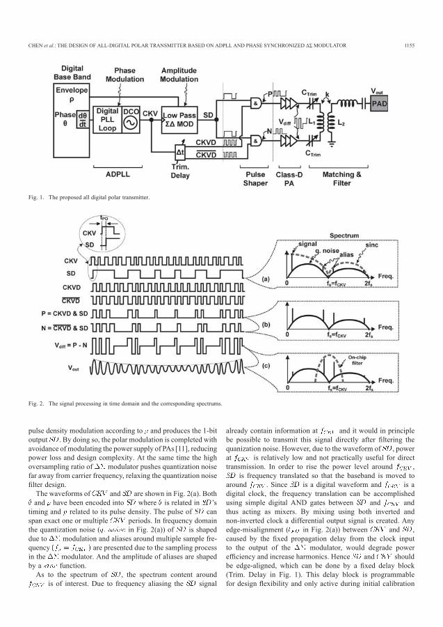
CHEN et al.: THE DESIGN OF ALL-DIGITAL POLAR TRANSMITTER BASED ON ADPLL AND PHASE SYNCHRONIZED MODULATOR 1155
Fig. 1. The proposed all digital polar transmitter.
Fig. 2. The signal processing in time domain and the corresponding spectrums.
pulse density modulation according to and produces the 1-bitoutput . By doing so, the polar modulation is completed withavoidance of modulating the power supply of PAs [11], reducingpower loss and design complexity. At the same time the highoversampling ratio of modulator pushes quantization noisefar away from carrier frequency, relaxing the quantization noiselter design.The waveforms of and are shown in Fig. 2(a). Bothand have been encoded into where is related in ’s
timing and related to its pulse density. The pulse of canspan exact one or multiple periods. In frequency domainthe quantization noise ( in Fig. 2(a)) of is shapeddue to modulation and aliases around multiple sample fre-quency are presented due to the sampling processin the modulator. And the amplitude of aliases are shapedby a function.As to the spectrum of , the spectrum content around
is of interest. Due to frequency aliasing the signal
already contain information at and it would in principlebe possible to transmit this signal directly after ltering thequanization noise. However, due to the waveform of , powerat is relatively low and not practically useful for directtransmission. In order to rise the power level around ,
is frequency translated so that the baseband is moved toaround . Since is a digital waveform and is adigital clock, the frequency translation can be accomplishedusing simple digital AND gates between and andthus acting as mixers. By mixing using both inverted andnon-inverted clock a differential output signal is created. Anyedge-misalignment ( in Fig. 2(a)) between and ,caused by the xed propagation delay from the clock inputto the output of the modulator, would degrade poweref ciency and increase harmonics. Hence and shouldbe edge-aligned, which can be done by a xed delay block(Trim. Delay in Fig. 1). This delay block is programmablefor design exibility and only active during initial calibration
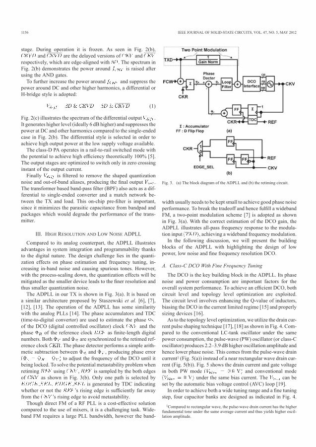
1156 IEEE JOURNAL OF SOLID-STATE CIRCUITS, VOL. 47, NO. 5, MAY 2012
stage. During operation it is frozen. As seen in Fig. 2(b),and are the delayed versions of and
respectively, which are edge-aligned with . The spectrum inFig. 2(b) demonstrates the power around is raised afterusing the AND gates.To further increase the power around and suppress the
power around DC and other higher harmonics, a differential orH-bridge style is adopted:
(1)
Fig. 2(c) illustrates the spectrum of the differential output .It generates higher level (ideally 6 dB higher) and suppresses thepower at DC and other harmonics compared to the single-endedcase in Fig. 2(b). The differential style is selected in order toachieve high output power at the low supply voltage available.The class-D PA operates in a rail-to-rail switched mode with
the potential to achieve high ef ciency theoretically 100% [5].The output stages are optimized to switch only in zero crossinginstant of the output current.Finally is ltered to remove the shaped quantization
noise and out-of-band aliases, producing the nal output .The transformer based band-pass lter (BPF) also acts as a dif-ferential to single-ended converter and a match network be-tween the TX and load. This on-chip pre- lter is important,since it minimizes the parasitic capacitance from bandpad andpackages which would degrade the performance of the trans-mitter.
III. HIGH RESOLUTION AND LOW NOISE ADPLL
Compared to its analog counterpart, the ADPLL illustratesadvantages in system integration and programmability thanksto the digital nature. The design challenge lies in the quanti-zation effects on phase estimation and frequency tuning, in-creasing in-band noise and causing spurious tones. However,with the process-scaling down, the quantization effects will bemitigated as the smaller device leads to the ner resolution andthus smaller quantization noise.The ADPLL in our TX is shown in Fig. 3(a). It is based on
a similar architecture proposed by Staszewski et al. [6], [7],[12], [13]. The operation of the ADPLL has some similaritywith the analog PLLs [14]. The phase accumulators and TDC(time-to-digital convertor) are used to estimate the phaseof the DCO (digital controlled oscillator) clock and thephase of the reference clock as nite-length digitalnumbers. Both and are synchronized to the retimed ref-erence clock . The phase detector performs a simple arith-metic subtraction between and , producing phase error
to adjust the frequency of the DCO until itbeing locked. To solve the potential metastability problem whenretiming using , is sampled by the both edgesof as shown in Fig. 3(b). Only one path is selected by
. is generated by TDC indicatingwhether or not the ’s rising edge is suf ciently far awayfrom the ’s rising edge to avoid metastability.Though direct FM of a RF PLL is a cost-effective solution
compared to the use of mixers, it is a challenging task. Wide-band FM requires a large PLL bandwidth, however the band-
Fig. 3. (a) The block diagram of the ADPLL and (b) the retiming circuit.
width usually needs to be kept small to achieve good phase noiseperformance. To break the tradeoff and hence ful ll a widebandFM, a two-point modulation scheme [7] is adopted as shownin Fig. 3(a). With the correct estimation of the DCO gain, theADPLL illustrates all-pass frequency response to the modula-tion input , achieving a wideband frequency modulation.In the following discussion, we will present the building
blocks of the ADPLL with highlighting the design of lowpower, low noise and ne frequency resolution DCO.
A. Class-C DCO With Fine Frequency Tuning
The DCO is the key building block in the ADPLL. Its phasenoise and power consumption are important factors for theoverall system performance. To achieve an ef cient DCO, bothcircuit level and topology level optimization are exploited.The circuit level involves enhancing the Q-value of inductors,biasing the DCO in the current limited regime [15] and properlysizing devices [16].As to the topology level optimization, we utilize the drain cur-
rent pulse shaping technique [17], [18] as shown in Fig. 4. Com-pared to the conventional LC-tank oscillator under the samepower consumption, the pulse-wave (PW) oscillator (or class-Coscillator) produces 2.2–3.9 dB higher oscillation amplitude andhence lower phase noise. This comes from the pulse-wave draincurrent1 (Fig. 5(a)) instead of a near rectangular wave drain cur-rent (Fig. 5(b)). Fig. 5 shows the drain current and gate voltagein both PW mode and conventional mode
under the same bias current. The can beset by the automatic bias voltage control (AVC) loop [19].In order to achieve both a wide tuning range and a ne tuning
step, four capacitor banks are designed as indicated in Fig. 4.1Compared to rectangular wave, the pulse-wave drain current has the higher
fundamental tone under the same average current and thus yields higher oscil-lation amplitude.
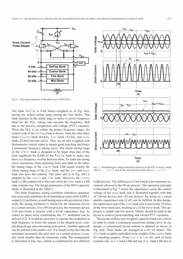
CHEN et al.: THE DESIGN OF ALL-DIGITAL POLAR TRANSMITTER BASED ON ADPLL AND PHASE SYNCHRONIZED MODULATOR 1157
Fig. 4. The main schematic of the pulse-wave (PW) DCO.
The bank is 4-bit binary-weighted as in Fig. 6(a),having the widest tuning range among the four banks. Thisbank operates in the initial stage to select a correct frequencyband for the PLL, taking into account the frequency shiftdue to the process, temperature and voltage (PVT) variation.When the PLL is set within the proper frequency range, thecontrol code of the bank is frozen. Then the other threebanks ( bank (64-bit), bank (32-bit), andbank (32-bit)) become active. They are all unit-weighted withthermometer control codes to ensure good matching and hencea monotonic frequency tuning curve. The whole tuning rangeof the bank is designed to be larger than that of theleast signi cant bit (LSB) of the bank to make surethere is a frequency overlap between them. To make the tuningcurve continuous when transiting from one bank to the other,the tuning range of the bank LSB equals exactly thewhole tuning range of the bank, and the andbank also have this relation. The same unit as in Fig. 6(b) isadopted by the and bank. However, thebank’s LSB contains 64 of this unit while the bank’s LSBonly contains one. The design parameters of the DCO capacitorbanks is illustrated in the Table I.The nite frequency tuning resolution introduces quantiza-
tion noise and contributes the in-band phase noise of the ADPLLoutput [12] and hence a small tuning step is always desired. Gen-erally the tuning resolution is limited by the minimum deviceof a certain process. For a 90 nm process, the minimum device(120 nm) forms a varactor with a 62-aF capacitance step. Toreduce its phase noise contribution, the modulator can beutilized [12]. It would be necessary to operate the modulator athigh frequency to lower the impact of the shaped noise, com-plicating design and consuming extra power. Another approachcan be utilized with smaller cost. It is based on the fact that theminimum increment (the grid size) in a certain process is usu-ally much smaller than the minimum width. The arrangementis illustrated in Fig. 6(c), which is constituted by two different
Fig. 5. Simulated gate voltage and drain current in (a) the PW or class-C modewhen and (b) the conventional mode when .
width devices. The difference is 5 nm which is the minimum in-crement allowed in the 90 nm process. The operation principleis illustrated in Fig. 7 where the capacitance versus the controlvoltage of the bank unit is illustrated together with thatof 120-nm devices and 125-nm devices. By doing so, a muchsmaller capacitance step (2-aF) can be ful lled. In this design,the capacitance step of the bank unit is practically 32 timesof the bank unit, resulting in a 32-bit bank. This ap-proach is simple and low power. Efforts should be paid in thelayout to achieve good matching and tolerate PVT variations.The layout of these unit-weighted capacitor banks are critical
in order to create a continuous monotonic tuning curve. In ourdesign, a symmetrical layout scheme is adopted as shown inFig. 6(d). Three banks are arranged as a 65 65 matrix. The
bank is tightly embedded in the middle of the bankfor matching purpose. From 1 to 64, each of themcontains one bank LSB and one bank LSB due to
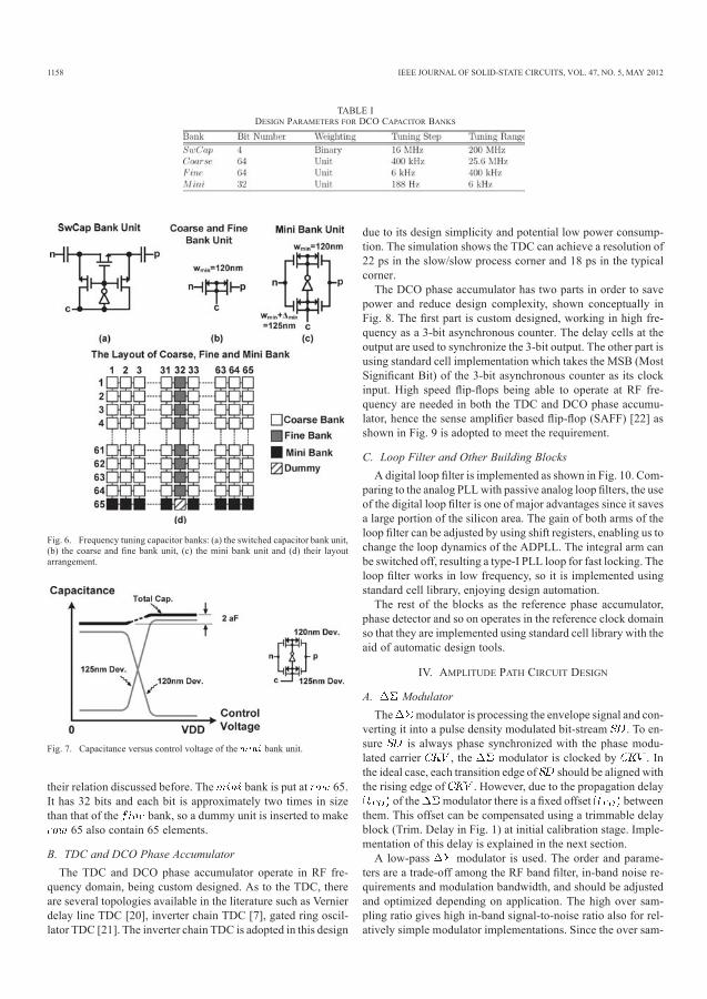
1158 IEEE JOURNAL OF SOLID-STATE CIRCUITS, VOL. 47, NO. 5, MAY 2012
TABLE IDESIGN PARAMETERS FOR DCO CAPACITOR BANKS
Fig. 6. Frequency tuning capacitor banks: (a) the switched capacitor bank unit,(b) the coarse and ne bank unit, (c) the mini bank unit and (d) their layoutarrangement.
Fig. 7. Capacitance versus control voltage of the bank unit.
their relation discussed before. The bank is put at 65.It has 32 bits and each bit is approximately two times in sizethan that of the bank, so a dummy unit is inserted to make
65 also contain 65 elements.
B. TDC and DCO Phase AccumulatorThe TDC and DCO phase accumulator operate in RF fre-
quency domain, being custom designed. As to the TDC, thereare several topologies available in the literature such as Vernierdelay line TDC [20], inverter chain TDC [7], gated ring oscil-lator TDC [21]. The inverter chain TDC is adopted in this design
due to its design simplicity and potential low power consump-tion. The simulation shows the TDC can achieve a resolution of22 ps in the slow/slow process corner and 18 ps in the typicalcorner.The DCO phase accumulator has two parts in order to save
power and reduce design complexity, shown conceptually inFig. 8. The rst part is custom designed, working in high fre-quency as a 3-bit asynchronous counter. The delay cells at theoutput are used to synchronize the 3-bit output. The other part isusing standard cell implementation which takes the MSB (MostSigni cant Bit) of the 3-bit asynchronous counter as its clockinput. High speed ip- ops being able to operate at RF fre-quency are needed in both the TDC and DCO phase accumu-lator, hence the sense ampli er based ip- op (SAFF) [22] asshown in Fig. 9 is adopted to meet the requirement.
C. Loop Filter and Other Building BlocksA digital loop lter is implemented as shown in Fig. 10. Com-
paring to the analog PLLwith passive analog loop lters, the useof the digital loop lter is one of major advantages since it savesa large portion of the silicon area. The gain of both arms of theloop lter can be adjusted by using shift registers, enabling us tochange the loop dynamics of the ADPLL. The integral arm canbe switched off, resulting a type-I PLL loop for fast locking. Theloop lter works in low frequency, so it is implemented usingstandard cell library, enjoying design automation.The rest of the blocks as the reference phase accumulator,
phase detector and so on operates in the reference clock domainso that they are implemented using standard cell library with theaid of automatic design tools.
IV. AMPLITUDE PATH CIRCUIT DESIGN
A. ModulatorThe modulator is processing the envelope signal and con-
verting it into a pulse density modulated bit-stream . To en-sure is always phase synchronized with the phase modu-lated carrier , the modulator is clocked by . Inthe ideal case, each transition edge of should be aligned withthe rising edge of . However, due to the propagation delay
of the modulator there is a xed offset betweenthem. This offset can be compensated using a trimmable delayblock (Trim. Delay in Fig. 1) at initial calibration stage. Imple-mentation of this delay is explained in the next section.A low-pass modulator is used. The order and parame-
ters are a trade-off among the RF band lter, in-band noise re-quirements and modulation bandwidth, and should be adjustedand optimized depending on application. The high over sam-pling ratio gives high in-band signal-to-noise ratio also for rel-atively simple modulator implementations. Since the over sam-
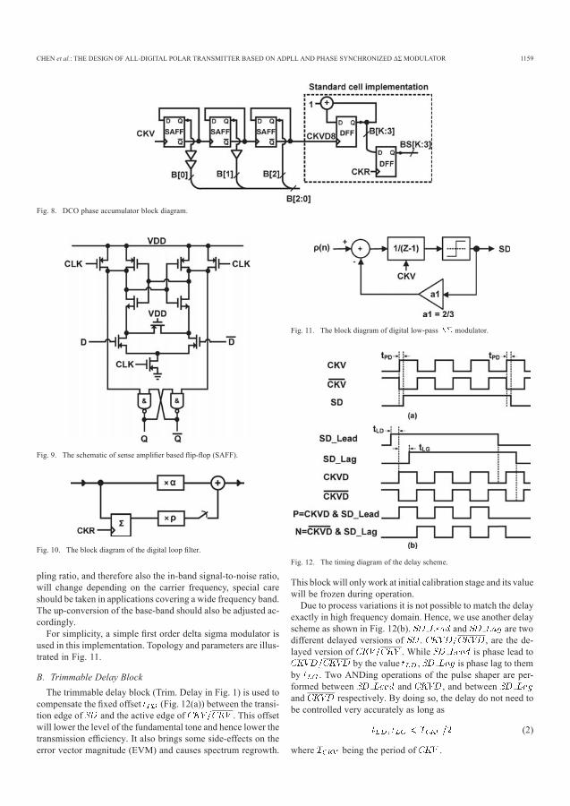
CHEN et al.: THE DESIGN OF ALL-DIGITAL POLAR TRANSMITTER BASED ON ADPLL AND PHASE SYNCHRONIZED MODULATOR 1159
Fig. 8. DCO phase accumulator block diagram.
Fig. 9. The schematic of sense ampli er based ip- op (SAFF).
Fig. 10. The block diagram of the digital loop lter.
pling ratio, and therefore also the in-band signal-to-noise ratio,will change depending on the carrier frequency, special careshould be taken in applications covering a wide frequency band.The up-conversion of the base-band should also be adjusted ac-cordingly.For simplicity, a simple rst order delta sigma modulator is
used in this implementation. Topology and parameters are illus-trated in Fig. 11.
B. Trimmable Delay BlockThe trimmable delay block (Trim. Delay in Fig. 1) is used to
compensate the xed offset (Fig. 12(a)) between the transi-tion edge of and the active edge of . This offsetwill lower the level of the fundamental tone and hence lower thetransmission ef ciency. It also brings some side-effects on theerror vector magnitude (EVM) and causes spectrum regrowth.
Fig. 11. The block diagram of digital low-pass modulator.
Fig. 12. The timing diagram of the delay scheme.
This blockwill only work at initial calibration stage and its valuewill be frozen during operation.Due to process variations it is not possible to match the delay
exactly in high frequency domain. Hence, we use another delayscheme as shown in Fig. 12(b). and are twodifferent delayed versions of . , are the de-layed version of . While is phase lead to
by the value , is phase lag to themby . Two ANDing operations of the pulse shaper are per-formed between and , and betweenand respectively. By doing so, the delay do not need tobe controlled very accurately as long as
(2)
where being the period of .
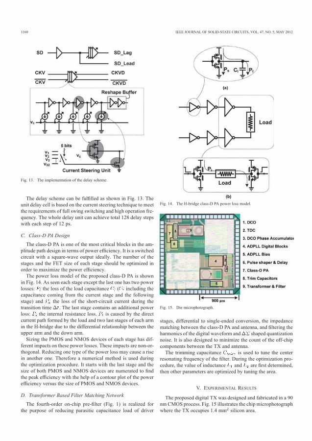
1160 IEEE JOURNAL OF SOLID-STATE CIRCUITS, VOL. 47, NO. 5, MAY 2012
Fig. 13. The implementation of the delay scheme.
The delay scheme can be ful lled as shown in Fig. 13. Theunit delay cell is based on the current steering technique to meetthe requirements of full swing switching and high operation fre-quency. The whole delay unit can achieve total 128 delay stepswith each step of 12 ps.
C. Class-D PA Design
The class-D PA is one of the most critical blocks in the am-plitude path design in terms of power ef ciency. It is a switchedcircuit with a square-wave output ideally. The number of thestages and the FET size of each stage should be optimized inorder to maximize the power ef ciency.The power loss model of the proposed class-D PA is shown
in Fig. 14. As seen each stage except the last one has two powerlosses: the loss of the load capacitance ( including thecapacitance coming from the current stage and the followingstage) and the loss of the short-circuit current during thetransition time . The last stage contains an additional powerloss: the internal resistance loss. is caused by the directcurrent path formed by the load and two last stages of each armin the H-bridge due to the differential relationship between theupper arm and the down arm.Sizing the PMOS and NMOS devices of each stage has dif-
ferent impacts on these power losses. These impacts are non-or-thogonal. Reducing one type of the power loss may cause a risein another one. Therefore a numerical method is used duringthe optimization procedure. It starts with the last stage and thesize of both PMOS and NMOS devices are numerated to ndthe peak ef ciency with the help of a contour plot of the poweref ciency versus the size of PMOS and NMOS devices.
D. Transformer Based Filter Matching Network
The fourth-order on-chip pre- lter (Fig. 1) is realized forthe purpose of reducing parasitic capacitance load of driver
Fig. 14. The H-bridge class-D PA power loss model.
Fig. 15. Die microphotograph.
stages, differential to single-ended conversion, the impedancematching between the class-D PA and antenna, and ltering theharmonics of the digital waveform and shaped quantizationnoise. It is also designed to minimize the count of the off-chipcomponents between the TX and antenna.The trimming capacitance is used to tune the center
resonating frequency of the lter. During the optimization pro-cedure, the value of inductance and are rst determined,then other parameters are optimized by tuning the area.
V. EXPERIMENTAL RESULTS
The proposed digital TX was designed and fabricated in a 90nm CMOS process. Fig. 15 illustrates the chip microphotographwhere the TX occupies 1.4 mm silicon area.
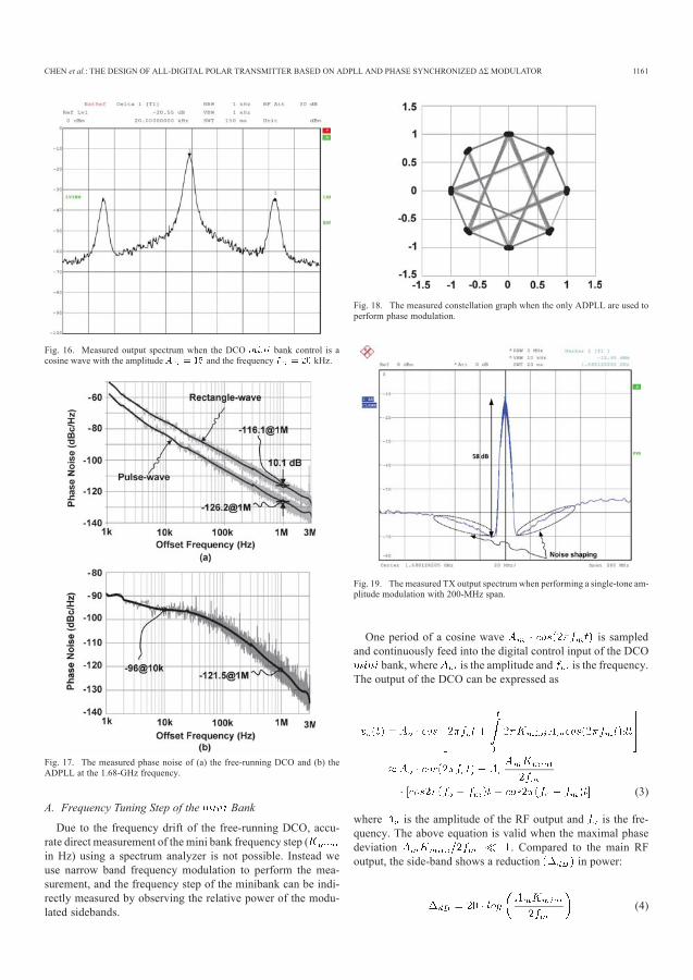
CHEN et al.: THE DESIGN OF ALL-DIGITAL POLAR TRANSMITTER BASED ON ADPLL AND PHASE SYNCHRONIZED MODULATOR 1161
Fig. 16. Measured output spectrum when the DCO bank control is acosine wave with the amplitude and the frequency kHz.
Fig. 17. The measured phase noise of (a) the free-running DCO and (b) theADPLL at the 1.68-GHz frequency.
A. Frequency Tuning Step of the Bank
Due to the frequency drift of the free-running DCO, accu-rate direct measurement of the mini bank frequency step (in Hz) using a spectrum analyzer is not possible. Instead weuse narrow band frequency modulation to perform the mea-surement, and the frequency step of the minibank can be indi-rectly measured by observing the relative power of the modu-lated sidebands.
Fig. 18. The measured constellation graph when the only ADPLL are used toperform phase modulation.
Fig. 19. The measured TX output spectrum when performing a single-tone am-plitude modulation with 200-MHz span.
One period of a cosine wave is sampledand continuously feed into the digital control input of the DCO
bank, where is the amplitude and is the frequency.The output of the DCO can be expressed as
(3)
where is the amplitude of the RF output and is the fre-quency. The above equation is valid when the maximal phasedeviation . Compared to the main RFoutput, the side-band shows a reduction in power:
(4)
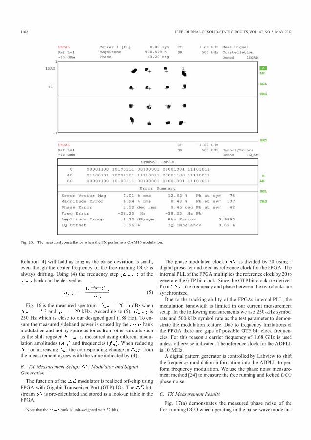
1162 IEEE JOURNAL OF SOLID-STATE CIRCUITS, VOL. 47, NO. 5, MAY 2012
Fig. 20. The measured constellation when the TX performs a QAM16 modulation.
Relation (4) will hold as long as the phase deviation is small,even though the center frequency of the free-running DCO isalways drifting. Using (4) the frequency step of the
bank can be derived as
(5)
Fig. 16 is the measured spectrum dB when2 and kHz. According to (5), is
250 Hz which is close to our designed goal (188 Hz). To en-sure the measured sideband power is caused by the bankmodulation and not by spurious tones from other circuits suchas the shift register, is measured using different modu-lation amplitudes and frequencies . When reducing
or increasing , the corresponding change in fromthe measurement agrees with the value indicated by (4).
B. TX Measurement Setup: Modulator and SignalGenerationThe function of the modulator is realized off-chip using
FPGA with Gigabit Transceiver Port (GTP) IOs. The bit-stream is pre-calculated and stored as a look-up table in theFPGA.2Note that the bank is unit-weighted with 32 bits.
The phase modulated clock is divided by 20 using adigital prescaler and used as reference clock for the FPGA. Theinternal PLL of the FPGAmultiplies the reference clock by 20 togenerate the GTP bit clock. Since the GTP bit clock are derivedfrom , the frequency and phase between the two clocks aresynchronized.Due to the tracking ability of the FPGAs internal PLL, the
modulation bandwidth is limited in our current measurementsetup. In the following measurements we use 250-kHz symbolrate and 500-kHz symbol rate as the test parameter to demon-strate the modulation feature. Due to frequency limitations ofthe FPGA there are gaps of possible GTP bit clock frequen-cies. For this reason a carrier frequency of 1.68 GHz is usedunless otherwise indicated. The reference clock for the ADPLLis 10 MHz.A digital pattern generator is controlled by Labview to shift
the frequency modulation information into the ADPLL to per-form frequency modulation. We use the phase noise measure-ment method [24] to measure the free running and locked DCOphase noise.
C. TX Measurement Results
Fig. 17(a) demonstrates the measured phase noise of thefree-running DCO when operating in the pulse-wave mode and
CHEN et al.: THE DESIGN OF ALL-DIGITAL POLAR TRANSMITTER BASED ON ADPLL AND PHASE SYNCHRONIZED MODULATOR 1163
Fig. 21. The measured time domain waveform of the modulator outputand the TX output.
the conventional mode respectively under the same power con-sumption of 6 mW from a 1.0-V power supply and the centerfrequency of 1.68 GHz. It veri es the bene t of the pulse-waveoscillator in terms of phase noise. As seen phase noise isreduced by 10.1 dB at 1-MHz offset frequency. Fig. 17(b) isthe measured phase noise of the ADPLL when operating at1.68 GHz with 12 mW power consumption from a 1-V powersupply. The integrated phase noise from 1 kHz to 2 MHz is 0.4degree calculated using
(6)
To examine the modulation accuracy of the ADPLL, a-QPSK modulation with 250-kHz symbol rate and raised
cosine lter is used as the test data. The phase informationis rst exacted and then converted to frequency deviation bydifferentiating operation. The frequency deviation is input intothe ADPLL and the output is then phase demodulated using asignal analyzer. The demodulated phase information is sampledto rebuild the demodulated constellation as shown in Fig. 18.The resulting RMS error EVM is 3.2%.Fig. 19 is the measured normalized TX output spectrumwhen
the TX only performs a single-tone amplitude modulation usingthe modulator. It illustrates the close in signal-to-noise ratio(SNR) and how the noise is shifted far away from the carrierfrequency, thus relaxing the lter design.Fig. 20 is the measured constellation when the TX performs
the QAM16 modulation. The RMS EVM is 7% which is worsethan the number when only ADPLL is doing frequency mod-ulation ( -QPSK).The degraded EVM is caused by severalmechanisms in the power ampli er. Insuf cient regulation ofthe on chip PA supply voltage makes the output power lowerthan expected at high output amplitude. During measurementit is also found the PA output impedance is data dependent,causing a nonlinear relation between the data and the outputamplitude. The full explanation for this degradation will be care-fully investigated in future research.Fig. 21 is the measured time domain outputs of the mod-
ulator and the TX after the on-chip pre- lter. Asseen, the pulse of can span one or multiple periods
TABLE IIPERFORMANCE COMPARISON AMONG THE PUBLISHED STATE-OF-THE-ART
POLAR TRANSMITTERS
m and SiGe BiCMOS.Including both transmitter and receiver.TX power ef ciency: the ratio of output power to total power of TX
front-end.
and it amplitude modulates the nal output . The delay be-tween and is caused by the amplitude path from theAND gates to the nal output and also caused by measurementcables.Table II summaries performance of the proposed transmitter
and compares other state-of-art designs mainly in terms of area,power consumption and ef ciency. As seen, our TX occupiessmall silicon area and achieves good TX power ef ciency. Thedigital TX consumes 58 mW power from a 1-V supply whendelivering a maximum 6.81-dBm output.
VI. CONCLUSION
An all-digital polar transmitter was proposed and imple-mented in a 90 nm digital CMOS process. It uses an ADPLLto perform wideband phase modulation, and a 1-bit low-pass
modulator for envelop modulation assuring a linear oper-ation. The modulated digital carrier is pulse-shaped to ful lla DC-free differential coding to enhance the power at thecarrier frequency and suppress other harmonics. The non-linear switched-mode class-D PA operating at constant powersupply delivers the ampli ed signal to the on-chip matchingand ltering network. Measurements justify the concept anddemonstrate good performance in terms of phase noise, areaand power ef ciency.
REFERENCES[1] L. R. Kahn, “Single-sideband transmission by envelope elimination
and restoration,” in Proc. IRE, Jul. 1952, vol. 40, no. 7, pp. 803–806.[2] J. Mehta, R. B. Staszewski, and O. Eliezer et al., “A 0.8 mm2 all-digital
SAW-less polar transmitter 65 nm EDGE SoC,” in IEEE ISSCC Dig.,Feb. 2010, pp. 58–59.
[3] M. Elliott, T. Montalvo, B. Jeffries, F. Murden, J. Strange, A. Hill,S. Nandipaku, and J. Harrebek, “A polar modulator transmitter forEDGE,” in IEEE ISSCC Dig., 2004, pp. 190–191.
[4] J. Choi, J. Yim, J. Yang, J. Kim, J. Cha, D. Kang, D. Kim, and B. Kim,“A -digitized polar RF transmitter,” IEEE Trans. Microw. TheoryTech., vol. 55, no. 12, pp. 2679–2690, Dec. 2007.
[5] M. Nielsen and T. Larsen, “A transmitter architecture based on DeltaSigma modulation and switch-mode power ampli cation,” IEEETrans. Circuits Syst. II, vol. 54, no. 8, pp. 735–739, Aug. 2007.
[6] R. B. Staszewski, J. L. Wallberg, S. Rezeq, C.-M. Hung, O. E. Eliezer,S. K. Vemulapalli, C. Fernando, K. Maggio, R. Staszewski, N. Barton,M.-C. Lee, P. Cruise, M. Entezari, K. Muhammad, and D. Leipold,“All-digital PLL and transmitter for mobile phone,” IEEE J. Solid-StateCircuits, vol. 40, no. 12, pp. 2469–2482, Dec. 2005.
1164 IEEE JOURNAL OF SOLID-STATE CIRCUITS, VOL. 47, NO. 5, MAY 2012
[7] R. B. Staszewski, K. Muhammad, D. Leipold, C.-M. Hung, Y.-C. Ho,J. L. Wallberg, C. Fernando, K. Maggio, R. Staszewski, T. Jung, J.Koh, S. John, I. Y. Deng, V. Sarda, O. Moreira-Tamayo, V. Mayega,R. Katz, O. Friedman, O. E. Eliezer, E. de-Obaldia, and P. T. Balsara,“All-digital TX frequency synthesizer and discrete-time receiver forBluetooth radio 130-nm CMOS,” IEEE J. Solid-State Circuits, vol. 39,no. 12, pp. 2278–2291, Dec. 2004.
[8] T.-P. Hung, J. Rode, L. E. Larson, and P. M. Asbeck, “Designof HBridge class-D power ampli ers for digital pulse modulationtransmitters,” IEEE Trans. Microw. Theory Tech., vol. 55, no. 12, pp.2845–2855, Dec. 2007.
[9] T. Johnson and S. P. Stapleton, “RF class-D ampli cation with band-pass Sigma Delta modulator drive signals,” IEEE Trans. Circuits Syst.I, vol. 53, no. 12, pp. 2507–2520, Dec. 2006.
[10] J. Chen, L. Rong, F. Jonsson, and L. R. Zheng, “All-digital transmitterbased on ADPLL and phase synchronized delta sigma modulator,” inIEEE RFIC Symp. Dig., Jul. 2011, pp. 1–4.
[11] Y. Wang, “An improved kahn transmitter architecture based ondeltasigma modulation,” in Proc. IEEE Int. Microwave Symp., Jun.2003, vol. 2, pp. 1327–1330.
[12] R. B. Staszewski, D. Leipold, K. Muhammad, and P. T. Balsara, “Dig-itally controlled oscillator (DCO)-based architecture for RF frequencysynthesis a deep-submicrometer CMOS process,” IEEE Trans. CircuitsSyst. II, vol. 50, no. 11, pp. 815–828, Nov. 2003.
[13] R. B. Staszewski and P. T. Balsara, “Phase-doma all-digital phase-locked loop,” IEEE Trans. Circuits Syst. II, vol. 52, no. 3, pp. 159–163,Mar. 2005.
[14] F. M. Gardner, Phaselock Techniques. New York: Wiley, 1979.[15] A. Hajimiri and T. H. Lee, “Design issues CMOS differential LC oscil-
lators,” IEEE J. Solid-State Circuits, vol. 34, no. 5, pp. 717–724, May1999.
[16] J. Chen, F. Jonsson, L. R. Zheng, H. Tenhunen, and D. Zhou, “Sizing ofMOS device LC-tank oscillators,” in Proc. IEEE Norchip, Nov. 2007,pp. 1–6.
[17] A. Mazzanti and P. Andreani, “A 1.4 mW 4.90-to-5.65 GHz class-CCMOS VCO with an average FoM of 194.5 dBc/Hz,” in IEEE ISSCCDig., Feb. 2008, pp. 474–476.
[18] J. Chen, F. Jonsson, H. Olsson, L. R. Zheng, and D. Zhou, “A currentshaping technique to lower phase noise LC oscillators,” Proc. IEEEElectronics, Circuits and Systems (ICECS), pp. 392–395, Aug. 2008.
[19] J. Chen, F. Jonsson, M. Carlsson, C. Hedenäs, and L. R. Zheng, “Alow power, startup ensured and constant amplitude class-C VCO 0.18m CMOS,” IEEE Microw. Wireless Compon. Lett., vol. 21, no. 8, pp.427–429, Aug. 2011.
[20] P. Dudek, S. Szczepanski, and J. Hat eld, “A high-resolution CMOStime-to-digital converter utilizing a Vernier delay line,” IEEE J. Solid-State Circuits, vol. 35, no. 2, pp. 240–247, Feb. 2000.
[21] B. Helal, M. Straayer, and M. H. Perrott, “A low jitter 1.6 GHz multi-plying DLL utilizing a scrambling time-to-digital converter and digitalcorrelation,” in IEEE VLSI Symp. Dig., Jun. 2007, pp. 166–167.
[22] B. N. Nikolic, V. G. Oklobdzija, V. Stajonovic, W. Jia, J. Chiu, andM. Leung, “Improved sense-ampli er-based ip- op: Design andmea-surements,” IEEE J. Solid-State Circuits, vol. 35, no. 6, pp. 876–884,Jun. 2000.
[23] K. Muhammad et al., “A low-cost quad-band single-chip GSM/GPRSradio 90 nm digital CMOS,” in IEEE RFIC Symp. Dig., Jun. 2009, pp.197–200.
[24] J. Chen, F. Jonsson, and L.-R. Zheng, “A fast and accurate phase noisemeasurement of free running oscillators using a single spectrum ana-lyzer,” in Proc. IEEE Norchip, Nov. 2010, pp. 1–4.
Jian Chen was born in Zhejiang, China, in 1981. Hereceived the M.S. degree in microelectronics fromFudan University, China, in 2006. Since 2007, hehas conducted a joint research project between iPackVinnova Excellence Center at the Royal Institute ofTechnology (KTH) and Catena Wireless ElectronicsAB, Sweden, working towards the Ph.D. degree.Since 2011, he worked as RF analog circuit de-
signer at Catena Wireless Electronics AB, Sweden.His main interests are phase noise optimization of RFoscillators, all-digital PLL (ADPLL) and all-digital
polar transmitter in CMOS technology.
Liang Rong (S’10) was born in Shanghai, China, in1981. He received the B.Eng. degree in informationengineering from Shanghai Jiao Tong University in2003 and the M.S.E.E. degree from Royal Instituteof Technology KTH, Sweden, in 2006. Since 2007,he has been a Ph.D. candidate supported by the iPackVinnova Excellence center, a joint research center inICT school of Royal Institute of Technology KTHSweden.His research is on low supply voltage, low power
high ef ciency digital polar ampli er. He is involvedwith digital transmitter wireless link project in iPack and working on high ef -ciency polar ampli er for multi-standard, multi-band communications.
Fredrik Jonsson was born in Gothenburg, Sweden,in 1972. He received the Ph.D. degree in electroniccircuits and devices from the Royal Institute of Tech-nology, KTH, Sweden, in 2008.His main interests are frequency synthesis, radio,
and mixed signal circuit design. Between 2000 and2006, he worked as circuit designer at Spirea AB andDiBcomAB. In 2006 and 2007, he was with the wire-less data group atMaxim Integrated products, US, fo-cusing on RF transmitters. Since 2010, he is the vicedirector of iPack Vinnova Excellence center where he
is also coordinating the Wireless Sensing and Tracking projects. Dr. Jonsson isthe co-founder of several companies and holds ve international patents.
Geng Yang received the B.S. and M.S. degreesfrom the College of Biomedical Engineering andInstrument Science, Zhejiang University, Hangzhou,China, in 2003 and 2006, respectively. He is cur-rently working toward the Ph.D. degree in iPackVinnova Excellence center, the school of Informa-tion and Communication Technology (ICT), RoyalInstitute of Technology (KTH), Stockholm, Sweden.He developed low power, low noise bio-electric
SoC sensors for body sensor network. His researchinterests include mixed-mode IC design for wearable
bio-devices, intelligent sensors, and low-power biomedical microsystem.
Li-Rong Zheng is a professor chair in media elec-tronics at the Swedish Royal Institute of Technology(KTH), founder and director of iPack Vinnova Excel-lence center, and Senior Specialist of Ericsson Net-works in Stockholm, Sweden. He received the Ph.D.degree in electronic system design from the RoyalInstitute of Technology (KTH), Stockholm, Swedenin 2001. Since then, he was with KTH as a researchfellow and project leader in Laboratory of Electronicsand Computer Systems. He became an associate pro-fessor in electronics system design in 2003 and a full
professor in media electronics at KTH in 2006. Dr. Zheng is a guest professor ofthe State Key Laboratory of ASICs and Systems at Fudan University in Chinasince 2008, and a distinguished professor of Fudan University since 2010. Hisresearch experience and interest includes electronic circuits and systems forambient intelligence and media applications, wireless SoC/SiP for sensing andidenti cation, and signal integrity issues in electronic systems. He has authoredand co-authored over 200 international reviewed publications, covering areasfrom electronic devices and thin lm technologies, VLSI circuit and system de-sign, to electronics systems and wireless sensors.