Embed Size (px)
Citation preview
M A S S A C H U S E T T S I N S T I T U T E O F T E C H N O L O G Y DEPARTMENT OF ELECTRICAL ENGINEERING AND COMPUTER SCIENCE
6.004 Computation Structures
Lab #1
General Information Lab assignments are due on Thursdays; check the on-line course calendar for the actual due date for each lab. Look at the on-line questions before you start to see what information you should collect while working on each lab. The lab software is written in Java and should run on any Java Virtual Machine supporting JDK 1.3 or higher. The courseware can be run on any Sun or Linux workstation. You can also download the courseware for your Linux or Windows 95/98/ME/NT/2000 machine at home. Introduction to JSim In this lab, we’ll be using a simulation program (JSim) to make some measurements of an N-channel mosfet (or “nfet” for short). JSim uses mathematical models of circuit elements to make predictions of how a circuit will behave both statically (DC analysis) and dynamically (transient analysis). The model for each circuit element is parameterized, e.g., the mosfet model includes parameters for the length and width of the mosfet as well as many parameters characterizing the physical aspects of the manufacturing process. For the models we are using, the manufacturing parameters have been derived from measurements taken at the integrated circuit fabrication facility and so the resulting predictions are quite accurate. To run Jsim a UNIX machine with the software installed, type the following at the UNIX prompt. % jsim & It can take a few moments for the Java runtime system to start up, please be patient! JSim takes as input a netlist that describes the circuit to be simulated. The initial JSim window is a very simple editor that lets you enter and modify your netlist. You may find the editor unsatisfactory for large tasks—it’s based on the JTextArea widget of the Java Swing toolkit that in some implementations has only rudimentary editing capabilities. If you use a separate editor to create your netlists, you can have JSim load your netlist files when it starts: % jsim filename … filename &
There are various handy buttons on the JSim toolbar:
Exit. Asks if you want to save any modified file buffers and then exits JSim.
New file. Create a new edit buffer called “untitled”. Any attempts to save this buffer will prompt the user for a filename.
6.004 Computation Structures - 1 - Lab #1

Open file. Prompts the user for a filename and then opens that file in its own edit buffer. If the file has already been read into a buffer, the buffer will be reloaded from the file (after asking permission if the buffer has been modified).
Close file. Closes the current edit buffer after asking permission if the buffer has been modified.
Reload file. Reload the current buffer from its source file after asking permission if the buffer has been modified. This button is useful if you are using an external editor to modify the netlist and simply want to reload a new version for simulation.
Save file. If any changes have been made, write the current buffer back to its source file (prompting for a file name if this is an untitled buffer created with the “new file” command). If the save was successful, the old version of the file is saved with a “.bak” extension.
Save file, specifying new file name. Like “Save file” but prompts for a new file name to use.
Save all files. Like “save file” but applied to all edit buffers.
Stop simulation. Clicking this control will stop a running simulation and display whatever waveform information is available.
Device-level simulation. Use a Spice-like circuit analysis algorithm to predict the behavior of the circuit described by the current netlist. After checking the netlist for errors, JSim will create a simulation network and then perform the requested analysis (i.e., the analysis you asked for with a “.dc” or “.tran” control statement). When the simulation is complete the waveform window is brought to the front so that the user can browse any results plotted by any “.plot” control statements.
Fast transient analysis. This simulation algorithm uses more approximate device models and solution techniques than the device-level simulator but should be much faster for large designs. For digital logic, the estimated logic delays are usually within 10% of the predictions of device-level simulation. This simulator only performs transient analysis.
Gate-level simulation. This simulation algorithm only knows about gates and logic values (instead of devices and voltages). We’ll use this feature later in the
6.004 Computation Structures - 2 - Lab #1
term when trying to simulate designs that contain too many mosfets to be simulated at the device level.
Switch to waveform window. In the waveform window this button switches to the editor window. Of course, you can accomplish the same thing by clicking on the border of the window you want in front, but sometimes using this button is less work.
Using information supplied in the checkoff file, check for specified node values at given times. If all the checks are successful, submit the circuit to the on-line assignment system. This mechanism will be used in Labs 2 through 7.
The waveform window shows various waveforms in one or more “channels.” Initially one channel is displayed for each “.plot” control statement in your netlist. If more than one waveform is assigned to a channel, the plots are overlaid on top of each using a different drawing color for each waveform. If you want to add a waveform to a channel simply add the appropriate signal name to the list appearing to the left of the waveform display (the name of each signal should be on a separate line). You can also add the name of the signal you would like displayed to the appropriate “.plot” statement in your netlist and rerun the simulation. If you simply name a node in your circuit, its voltage is plotted. You can also ask for the current through a voltage source by entering “I(Vid)”. The waveform window has several other buttons on its toolbar:
Select the number of displayed channels; choices range between 1 and 16.
Print. Prints the contents of the waveform window (in color if you have a color printer!). If you are using Athena, you have to print to a file and then send the file to the printer: select "file" in the print dialog, supply the name you'd like to use for the plot file, then click "print". You can send the file to one of the printers in the lab using "lpr", e.g., "lpr -Pcs foo.plot".
You can zoom and pan over the traces in the waveform window using the control found along the bottom edge of the waveform display:
zoom in. Increases the magnification of the waveform display. You can zoom in around a particular point in a waveform by placing the cursor at the point on the trace where you want to zoom in and typing upper-case “X”.
zoom out. Decreases the magnification of the waveform display. You can zoom out around a particular point in a waveform by placing the cursor at the point on the trace where you want to zoom out and typing lower-case “x”.
6.004 Computation Structures - 3 - Lab #1

surround. Sets the magnification so that the entire waveform will be visible in the waveform window.
The scrollbar at the bottom of the waveform window can be used to scroll through the waveforms. The scrollbar will be disabled if the entire waveform is visible in the window. You can recenter the waveform display about a particular point by placing the cursor at the point which you want to be at the center of the display and typing “c”. The JSim netlist format is quite similar to that used by Spice, a well-known circuit simulator. Each line of the netlist is one of the following:
A comment line, indicated by an “*” (asterisk) as the first character. Comment lines (and also blank lines) are ignored when JSim processes your netlist. You can also add comments at the end of a line by preceding the comment with the characters “//” (C++- or Java-style comments). All characters starting with “//” to the end of the line are ignored. Any portion of a line or lines can be turned into a comment by enclosing the text in “/*” and “*/” (C-style comments). A continuation line, indicated by a “+” (plus) as the first character. Continuation lines are treated as if they had been typed at the end of the previous line (without the “+” of course). There’s no limitation on the length of an input line but sometimes it’s easier to edit long lines if you use continuation lines. Note that “+” also continues “*” comment lines! A control statement, indicated by a “.” (period) as the first character. Control statements provide information about how the circuit is to be simulated. We’ll describe the syntax of the different control statements as we use them below. A circuit element, indicated by a letter as the first character. The first letter indicates the type of circuit element, e.g., “r” for resistor, “c” for capacitor, “m” for mosfet, “v” for voltage source. The remainder of the line specifies which circuit nodes connect to which device terminals and any parameters needed by that circuit element. For example the following line describes a 1000Ω resistor called “R1” that connects to nodes A and B. R1 A B 1k
Note that numbers can be entered using engineering suffixes for readability. Common suffixes are “k”=1000, “u”=1E-6, “n”=1E-9 and “p”=1E-12.
Characterizing MOSFETs Let’s make some measurements of an nfet by hooking it up to a couple of voltage sources to generate different values for VGS and VDS:
6.004 Computation Structures - 4 - Lab #1

We’ve included an ammeter (built from a 0v voltage source) so we can measure IDS, the current flowing through the mosfet from its drain terminal to its source terminal. Here’s the translation of the schematic into our netlist format:
* plot Ids vs. Vds for 5 different Vgs values .include "nominal.jsim" Vmeter vds drain 0v Vds vds 0 0v Vgs gate 0 0v * N-channel mosfet used for our test M1 drain gate 0 0 NENH W=1.2u L=600n .dc Vds 0 5 .1 Vgs 0 5 1 .plot I(Vmeter)
The first line is a comment. The second line is a control statement that directs JSim to include a netlist file containing the mosfet model parameters for the manufacturing process we’ll be targeting this semester. The next three lines specify three voltage sources; each voltage source specifies the two terminal nodes and the voltage we want between them. Note that the reference node for the circuit (marked with a ground symbol in the schematic) is always called “0”. The “v” following the voltage specification isn’t a legal scale factor and will be ignored by JSim; we use it just to remind ourselves what that last number is the voltage of the voltage source. All three sources are initially set to 0 volts but the voltage for the Vds and Vgs sources will be changed later when JSim processes the “.dc” control statement. We can ask JSim to plot the current through voltage sources which is how we’ll see what IDS is for different values of VGS and VDS. We could just ask for the current of the VDS voltage source, but the sign would be wrong since JSim uses the convention that positive current flows from the positive to negative terminal of a voltage source. So we introduce a 0-volt source with its terminals oriented to produce the current sign we’re looking for. The sixth line is the mosfet itself, where we’ve specified (in order) the names of the drain, gate, source and substrate nodes of the mosfet. The next item names the set of model parameters JSim should use when simulating this device; specify “NENH” to create an nfet and “PENH” for a P-channel mosfet (“pfet”). The final two entries specify the width and length of the mosfet. Note that the dimensions are in microns (1E-6 meters) since we’ve specified the “u” scale factor as a suffix. Don’t forget the “u” or your mosfets will be meters long! You can always use scientific notation (e.g., 1.2E-6) if suffixes are confusing. The seventh line is a control statement requesting a DC analysis of the circuit made with different settings for the Vds and Vgs voltage sources: the voltage of Vds is swept from 0V to 5V in .1V
6.004 Computation Structures - 5 - Lab #1

steps, and the voltage of Vgs is swept from 0V to 5V in 1V steps. Altogether 51 * 6 separate measurements will be made. The eighth and final line requests that JSim plot the current through the voltage source named “Vmeter”. JSim knows how to plot the results from the dual voltage sweep requested on the previous line: it will plot I(Vmeter) vs. the voltage of source Vds for each value of voltage of the source Vgs—there will be 6 plots in all, each consisting of 51 connected data points. After you enter the netlist above, you might want to save your efforts for later use by using the “save file” button. To run the simulation, click the “device-level simulation” button on the tool bar. After a pause, a waveform window will pop up where we can take some measurements. As you move the mouse over the waveform window, a moving cursor will be displayed on the first waveform above the mouse’s position and a readout giving the cursor coordinates will appear in the upper left hand corner of the window. To measure the delta between two points, position the mouse so the cursor is on top of the first point. Now click left and drag the mouse (i.e., move the mouse while holding its left button down) to bring up a second cursor that you can then position over the second point. The readout in the upper left corner will show the coordinates for both cursors and the delta between the two coordinates. You can return to one cursor by releasing the left button. We’re now ready to make some measurements:
(A) To get a sense of how well the channel of a turned-on mosfet conducts, let’s estimate the effective resistance of the channel while the mosfet is in the linear conduction region. We’ll use the Vgs = 5V curve (the upper-most plot in the window). The actual effective resistance is given by ∂VDS/∂IDS and clearly depends on which VDS we choose. Let’s use VDS = 1.2V. We could determine the resistance graphically from the slope of a line tangent to the IDS curve at VDS = 1.2V. But we can get a rough idea of the channel resistance by determining the slope of a line passing through the origin and the point we chose on the IDS curve, i.e., 1.2V/ IDS. Of course, the channel resistance depends on the dimensions of the mosfet we used to make the measurement. For mosfets, their IDS is proportional to W/L where W is the width of the mosfet (1.2 microns in this example) and L is the length (0.6 microns in this example). When reporting the effective channel resistance, it’s useful to report the sheet resistance, i.e., the resistance when W/L = 1. That way you can easily estimate the effective channel resistance for size device by scaling the sheet resistance appropriately. Since W/L = 2 for the device you measured, it conducted twice as much current and has half the channel resistance as a device with W/L = 1, so you need to double the channel resistance you computed above in order to estimate the effective channel sheet resistance. Use the on-line questions page for this lab to report the value for IDS that you measured and the effective channel sheet resistance you calculated from that measurement.
(B) Now let’s see how well the mosfet turns “off.” Take some measurements of IDS at various
points along the VGS=0V curve (the bottom-most plot in the window). Notice that they aren’t zero! Mosfets do conduct minute amounts of current even when officially “off”, a phenomenon called “subthreshold conduction.” While negligible for most purposes, this current is significant if we are trying to store charge on a capacitor for long periods of time
6.004 Computation Structures - 6 - Lab #1

(this is what DRAMs try to do). Make a measurement of IDS when VGS=0V and VDS=2.5V. Based on this measurement report how long it would take for a .05pF capacitor to discharge from 5V to 2.5V, i.e., to change from a valid logic “1” to a voltage in the forbidden zone. Recall from 6.002 that Q = CV, so we can estimate the discharge time as . So if our mosfet switch controls access to the storage capacitor, you can see we’ll need to refresh the capacitor’s charge at fairly frequent intervals.
)/( OFFIVCt ∆=∆
Gate-level timing The following JSim netlist shows how to define your own circuit elements using the “.subckt” statement:
* circuit for Lab#1, parts D thru I .include "nominal.jsim" * 2-input NAND: inputs are A and B, output is Z .subckt nand2 a b z MPD1 z a 1 0 NENH sw=8 sl=1 MPD2 1 b 0 0 NENH sw=8 sl=1 MPU1 z a vdd vdd PENH sw=8 sl=1 MPU2 z b vdd vdd PENH sw=8 sl=1 .ends * INVERTER: input is A, output is Z .subckt inv a z MPD1 z a 0 0 NENH sw=16 sl=1 MPU1 z a vdd vdd PENH sw=16 sl=1 .ends
The “.subckt” statement introduces a new level of netlist. All lines following the “.subckt” up to the matching “.ends” statement will be treated as a self-contained subcircuit. This includes model definitions, nested subcircuit definitions, electrical nodes and circuit elements. The only parts of the subcircuit visible to the outside world are its terminal nodes which are listed following the name of the subcircuit in the “.subckt” statement:
.subckt name terminals… * internal circuit elements are listed here .ends
In the example netlist, two subcircuits are defined: “nand2” which has 3 terminals (named “a”, “b” and “z” inside the nand2 subcircuit) and “inv” which has 2 terminals (named “a” and “z”). Once the definitions are complete, you can create an instance of a subcircuit using the “X” circuit element:
Xid nodes… name
where name is the name of the circuit definition to be used, id is a unique name for this instance of the subcircuit and nodes… are the names of electrical nodes that will be hooked up to the terminals of the subcircuit instance. There should be the same number of nodes listed in the “X” statement as there were terminals in the “.subckt” statement that defined name. For example, here’s a short netlist that instantiates 3 NAND gates (called “g0”, “g1” and “g2”):
6.004 Computation Structures - 7 - Lab #1

Xg0 d0 ctl z0 nand2 Xg1 d1 ctl z1 nand2 Xg2 d2 ctl z2 nand2
The node “ctl” connects to all three gates; all the other terminals are connected to different nodes. Note that any nodes that are private to the subcircuit definition (i.e., nodes used in the subcircuit that don’t appear on the terminal list) will be unique for each instantiation of the subcircuit. For example, there is a private node named “1” used inside the nand2 definition. When JSim processes the three “X” statements above, it will make three independent nodes called “xg0.1”, “xg1.1” and “xg2.1”, one for each of the three instances of nand2. There is no sharing of internal elements or nodes between multiple instances of the same subcircuit. It is sometimes convenient to define nodes that are shared by the entire circuit, including subcircuits; for example, power supply nodes. The ground node “0” is such a node; all references to “0” anywhere in the netlist refer to the same electrical node. The included netlist file nominal.JSim defines another shared node called “vdd” using the following statements:
.global vdd VDD vdd 0 3.3v
The example netlist above uses “vdd” whenever a connection to the power supply is required. The other new twist introduced in the example netlist is the use of symbolic dimensions for the mosfets (“SW=” and “SL=”) instead of physical dimensions (“W=” and “L=”). Symbolic dimensions specify multiples of a parameter called SCALE, which is also defined in nominal.JSim:
.option SCALE=0.6u
So with this scale factor, specifying “SW=8” is equivalent to specifying “W=4.8u.” Using symbolic dimensions is encouraged since it makes it easier to determine the W/L ratio for a mosfet (the current through a mosfet is proportional to W/L) and it makes it easy to move the design to a new manufacturing process that uses different dimensions for its mosfets. Note that in almost all instances “SL=1” since increasing the channel length of a mosfet reduces its current carrying capacity, not something we’re usually looking to do. We’ll need to keep the PN junctions in the source and drain diffusions reverse biased to ensure that the mosfets stay electrically isolated, so the substrate terminal of nfet (those specifying the “NENH” model) should always be hooked to ground (node “0”). Similarly the substrate terminal of pfet (those specifying the “PENH” model) should always be hooked to the power supply (node “vdd”). With the preliminaries out of the way, we can tackle some design issues:
(C) To maximize noise margins we want to have the transition in the voltage transfer characteristic (VTC) of the nand2 gate centered halfway between ground and the power supply voltage (3.3V). To determine the VTC for nand2, we’ll perform a dc analysis to plot the gate’s output voltage as a function of the input voltage using the following additional netlist statements:
6.004 Computation Structures - 8 - Lab #1

* dc analysis to create VTC Xtest vin vin vout nand2 Vin vin 0 0v Vol vol 0 0.3v // make measurements easier! Voh voh 0 3v // see part (D) .dc Vin 0 3.3 .005 .plot vin vout voh vol Combine this netlist fragment with the one given at the start of this section and run the simulation. To center the VTC transition, keep the size of the nfet in the nand2 definition as “SW=8 SL=1” and adjust the width of both pfets until the plots for vin and vout intersect at about 1.65 volts. Just try different integral widths (i.e, 9, 10, 11, …). Report the integral width that comes closest to having the curves intersect at 1.65V.
(D) The noise immunity of a gate is the smaller of the low noise margin (VIL − VOL) and the high noise margin (VOH − VIH). If we specify VOL = 0.3V and VOH = 3.0V, what is the largest possible noise immunity we could specify and still have the “improved” NAND gate of part (C) be a legal member of the logic family? Hint: to measure the low noise margin, use the VTC to determine what VIN has to be in order for VOUT to be 3V, and then subtract VOL (0.3V) from that number. To measure the high noise margin, use the VTC to determine what VIN has to be in order for VOUT to be 0.3V, and then subtract that number from VOH (3.0V). We’ve added some voltage sources corresponding to VOL and VOH to make it easier to make the measurements on the VTC plot. NOTE: make these measurements using your “improved” nand2 gate that has the centered VTC, i.e., with the updated widths for the PFETS.
Now that we have the mosfets ratioed properly to maximize noise immunity, let’s measure the contamination time (tC) and propagation time (tP) of the nand2 gate. The contamination delay, tCD, for the nand2 gate will be a lower bound for all the tC measurements we make. Similarly, the propagation delay, tPD, for the nand2 gate will be an upper bound for all the tP measurements. Recall that the contamination time is the period of output validity after the inputs have become invalid. So for nand2:
tC-FALL = time elapsed from when input > VIL to when output < VOH tC-RISE = time elapsed from when input < VIH to when output > VOL tC = min(tC-RISE, tC-FALL)
Similarly the propagation time is the period of output invalidity after the inputs have become valid. So for nand2:
tP-RISE = time elapsed from when input ≤ VIL to when output ≥ VOH tP-FALL = time elapsed from when input ≥ VIH to when output ≤ VOL tP = max(tP-RISE, tP-FALL)
Finally, the rise and fall times indicate how long it takes the output to transition between valid logic levels:
6.004 Computation Structures - 9 - Lab #1
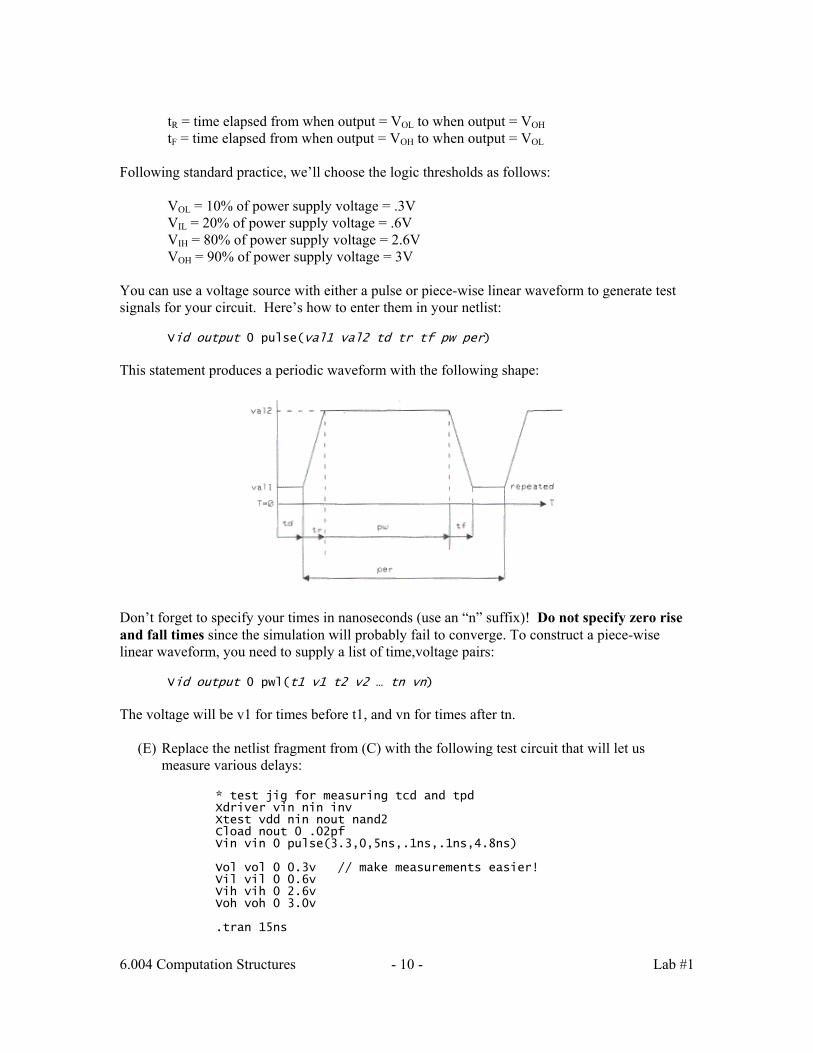
tR = time elapsed from when output = VOL to when output = VOH tF = time elapsed from when output = VOH to when output = VOL
Following standard practice, we’ll choose the logic thresholds as follows:
VOL = 10% of power supply voltage = .3V VIL = 20% of power supply voltage = .6V VIH = 80% of power supply voltage = 2.6V VOH = 90% of power supply voltage = 3V
You can use a voltage source with either a pulse or piece-wise linear waveform to generate test signals for your circuit. Here’s how to enter them in your netlist: Vid output 0 pulse(val1 val2 td tr tf pw per) This statement produces a periodic waveform with the following shape:
Don’t forget to specify your times in nanoseconds (use an “n” suffix)! Do not specify zero rise and fall times since the simulation will probably fail to converge. To construct a piece-wise linear waveform, you need to supply a list of time,voltage pairs: Vid output 0 pwl(t1 v1 t2 v2 … tn vn)
The voltage will be v1 for times before t1, and vn for times after tn.
(E) Replace the netlist fragment from (C) with the following test circuit that will let us
measure various delays: * test jig for measuring tcd and tpd Xdriver vin nin inv Xtest vdd nin nout nand2 Cload nout 0 .02pf Vin vin 0 pulse(3.3,0,5ns,.1ns,.1ns,4.8ns) Vol vol 0 0.3v // make measurements easier!
Vil vil 0 0.6v Vih vih 0 2.6v Voh voh 0 3.0v
.tran 15ns
6.004 Computation Structures - 10 - Lab #1

.plot vin .plot nin nout vol vil vih voh NOTE: make these measurements using your “improved” nand2 gate that has the centered VTC, i.e., with the updated widths for the pfets. We use an inverter to drive the nand2 input since we would normally expect the test gate to be driven by the output of another gate (there are some subtle timing effects that we’ll miss if we drive the input directly with a voltage source). Run the simulation and measure the contamination and propagation delays for both the rising and falling output transitions. (You’ll need to zoom in on the transitions in order to make an accurate measurement.) Combine as described above to produce estimates for tC and tP. Measure and report the output rise and fall times.
(F) We mentioned several times in lecture the desire to have our circuits operate reliably over
a wide range of environmental conditions. We can have JSim simulate our test circuit at different temperature by adding a “.temp” control statement to the netlist. Normally JSim simulates the circuit at room temperature (25°C), but we can simulate the circuit at, say, 85°C by adding the following to our netlist: .temp 85 For many consumer products, designs are tested in the range of 0°C to 100°C. Repeat your measurements of part (E) at the two extremes of temperature and report your findings. Recompute your estimates for tC and tP indicating which measurement(s) determined your final choice for the two delays. Roughly speaking, what percentage difference (sometimes called the derating factor) did changing the temperature produce in your delay estimates? So if you were working for Intel, the Pentium that ran at 800Mhz in the lab would be sold to the customers rated at what speed? This is why you can usually get away with overclocking your CPU—it’s been rated for operation under much more severe environmental conditions than you’re probably running it at!
For comparison, here’s a chart showing the process, temperature and power supply voltage derating factors for a commercial manufacturing process. The process-derating factor is used to estimate the effects of manufacturing variations (e.g., doping levels or etching rates) on the performance of the circuit. Derating Factors for Process Variation
Process Conditions Derating Factor Slow 1.22
Nominal 1.00 Fast 0.81
6.004 Computation Structures - 11 - Lab #1

Power Supply Voltage (VDD) Temperature (oC) 4.25 V 4.50 V 4.75 V 5.0 V 5.25 V 5.50 V 5.75 V -40 0.92 0.89 0.85 0.83 0.80 0.78 0.76 0 1.05 1.01 0.97 0.93 0.91 0.89 0.86
25 1.13 1.08 1.04 1.00 0.97 0.95 0.93 85 1.27 1.22 1.18 1.13 1.10 1.06 1.04
100 1.30 1.24 1.20 1.15 1.12 1.09 1.06 125 1.34 1.29 1.23 1.19 1.16 1.12 1.10
You can combine information from the two tables by multiplying the appropriate factor from each table to get an overall derating factor. Derating factors less than 1 indicate smaller delays and hence faster circuit operation. Derating factors greater than 1 indicate longer delays and hence slower circuit operation.
(G) Using the tables above, in the worst case (slow process, low power supply voltage and high temperature), how do the expected delays compare to a circuit operating under “normal” conditions. How much faster would expect the circuit to run under optimal conditions? Between worst and best case conditions, what’s the expected overall change in circuit performance?
The delays we just measured are sometimes called intrinsic delays since they characterize the speed of the gate with essentially no output load. A second delay measurement, called the extrinsic delay and usually expressed in units of (ns of delay)/(pf of output load), accounts for the extra delay introduced when the gate has to drive the additional capacitive load provided by metal interconnect and other gates to which the output is connected. The total delay of a loaded gate can then be computed from the sum of its intrinsic and extrinsic delays.
(H) Return to room temperature (get rid of the “.temp” statement) and increase Cload from 0.02pf to .2pf, which represents a fairly large output load for the process technology we’re using. Compute the extra propagation delay for both output transitions due to the heavier output load and report your estimate for the extrinsic delays in terms of ns/pf. For comparison, here’s a delay table for a 2-input NAND gate in the same commercial process used for comparison above:
Cell Size and Delay Information
Cell Grid Transistor Propagation Delay Extrinsic Intrinsic Z ↓ 1.66 ns/pF 0.19 ns ND2 3 4 Z ↑ 0.79 ns/pF 0.14 ns
CMOS logic-gate design As the final part of this lab, your mission is to design and test a CMOS circuit that implements the XYZZY(A,B,C) using nfets and pfets. The truth table for XYZZY is shown below:
6.004 Computation Structures - 12 - Lab #1
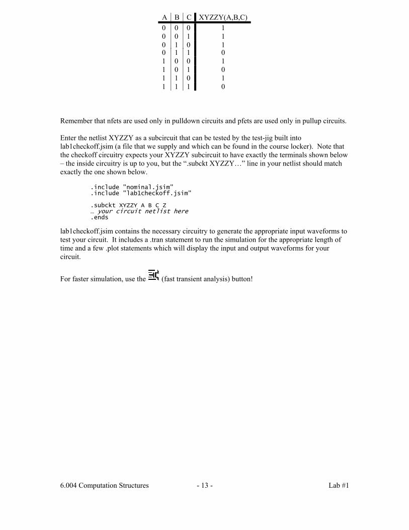
0 1 1 0 1 0 0 1 1 0 1 0 1 1 0 1 1 1 1 0
Remember that nfets are used only in pulldown circuits and pfets are used only in pullup circuits. Enter the netlist XYZZY as a subcircuit that can be tested by the test-jig built into lab1checkoff.jsim (a file that we supply and which can be found in the course locker). Note that the checkoff circuitry expects your XYZZY subcircuit to have exactly the terminals shown below – the inside circuitry is up to you, but the “.subckt XYZZY…” line in your netlist should match exactly the one shown below. .include "nominal.jsim" .include "lab1checkoff.jsim" .subckt XYZZY A B C Z … your circuit netlist here .ends
lab1checkoff.jsim contains the necessary circuitry to generate the appropriate input waveforms to test your circuit. It includes a .tran statement to run the simulation for the appropriate length of time and a few .plot statements which will display the input and output waveforms for your circuit.
For faster simulation, use the (fast transient analysis) button!
6.004 Computation Structures - 13 - Lab #1
A B C XYZZY(A,B,C)0 0 0 1 0 0 1 1 0 1 0 1