Embed Size (px)
Citation preview

SW
VIN
GND
BOOT
FB
COMP
TPS54360
EN
RT/CLK
VIN
VOUT
Copyright © 2017, Texas Instruments Incorporated
0
10
20
30
40
50
60
70
80
100
0 0.5 1.0 1.5 2.0
I - Output Current - AO
Eff
icie
nc
y -
%
2.5 3.0
90
4.03.5
5 V 3.3 V
V = 5 V, sw = 600 kHzOUT f
V = 3.3 V,OUT fsw = 300 kHz
V = 12 VIN
Product
Folder
Order
Now
Technical
Documents
Tools &
Software
Support &Community
An IMPORTANT NOTICE at the end of this data sheet addresses availability, warranty, changes, use in safety-critical applications,intellectual property matters and other important disclaimers. PRODUCTION DATA.
TPS54360SLVSBB4F –AUGUST 2012–REVISED MARCH 2017
TPS54360 60 V Input, 3.5 A, Step Down DC-DC Converter with Eco-mode™
1
1 Features1• 4.5 V to 60 V (65 V Abs Max) Input Range• 3.5 A Continuous Current, 4.5 A Minimum Peak
Inductor Current Limit• Current Mode Control DC-DC Converter• 92-mΩ High-Side MOSFET• High Efficiency at Light Loads with Pulse Skipping
Eco-mode™• Low Dropout at Light Loads with Integrated BOOT
Recharge FET• 146 μA Operating Quiescent Current• 2 μA Shutdown Current• 100 kHz to 2.5 MHz Fixed Switching Frequency• Synchronizes to External Clock• Adjustable UVLO Voltage and Hysteresis• Internal Soft-Start• Accurate Cycle-by-Cycle Current Limit• Thermal, Overvoltage, and Frequency Foldback
Protection• 0.8 V 1% Internal Voltage Reference• 8-Terminal HSOP with PowerPAD™ Package• –40°C to 150°C TJ Operating Range• Create a Custom Design using the TPS54360 with
the WEBENCH® Power Designer
2 Applications12 V, 24 V and 48 V Industrial, Automotive andCommunications Power Systems
3 DescriptionThe TPS54360 is a 60 V, 3.5 A, step down regulatorwith an integrated high side MOSFET. The devicesurvives load dump pulses up to 65V per ISO 7637.Current mode control provides simple externalcompensation and flexible component selection. Alow ripple pulse skip mode reduces the no loadsupply current to 146 μA. Shutdown supply current isreduced to 2 μA when the enable pin is pulled low.
Undervoltage lockout is internally set at 4.3 V but canbe increased using the enable pin. The output voltagestart up ramp is internally controlled to provide acontrolled start up and eliminate overshoot.
A wide switching frequency range allows eitherefficiency or external component size to be optimized.Frequency foldback and thermal shutdown protectsinternal and external components during an overloadcondition.
The TPS54360 is available in an 8-terminal thermallyenhanced HSOP PowerPAD™ package.
Device InformationORDER NUMBER PACKAGE BODY SIZE
TPS54360 HSOP (8) 4.89 mm x 3.9 mm
spacerSimplified Schematic
Efficiency vs Load Current

2
TPS54360SLVSBB4F –AUGUST 2012–REVISED MARCH 2017 www.ti.com
Product Folder Links: TPS54360
Submit Documentation Feedback Copyright © 2012–2017, Texas Instruments Incorporated
Table of Contents1 Features .................................................................. 12 Applications ........................................................... 13 Description ............................................................. 14 Revision History..................................................... 25 Pin Configuration and Functions ......................... 46 Specifications......................................................... 5
6.1 Absolute Maximum Ratings ...................................... 56.2 ESD Ratings.............................................................. 56.3 Recommended Operating Conditions....................... 56.4 Thermal Information .................................................. 56.5 Electrical Characteristics........................................... 66.6 Timing Requirements ................................................ 76.7 Typical Characteristics .............................................. 7
7 Detailed Description ............................................ 117.1 Overview ................................................................. 117.2 Functional Block Diagram ....................................... 12
7.3 Feature Description................................................. 127.4 Device Functional Modes........................................ 23
8 Application and Implementation ........................ 258.1 Application Information............................................ 258.2 Typical Application .................................................. 25
9 Power Supply Recommendation ........................ 3710 Layout................................................................... 38
10.1 Layout Guidelines ................................................. 3810.2 Layout Example .................................................... 38
11 Device and Documentation Support ................. 3911.1 Documentation Support ........................................ 3911.2 Receiving Notification of Documentation Updates 3911.3 Community Resources.......................................... 3911.4 Trademarks ........................................................... 3911.5 Electrostatic Discharge Caution............................ 39
12 Mechanical, Packaging, and OrderableInformation ........................................................... 39
4 Revision HistoryNOTE: Page numbers for previous revisions may differ from page numbers in the current version.
Changes from Revision E (March 2014) to Revision F Page
• Added the WEBENCH information in the Features, Detailed Design Procedure, and Device Support sections .................. 1• Changed the Handling Ratings table to the ESD Ratings table ............................................................................................. 5• Moved the Storage temperature to the Absolute Maximum Ratings table............................................................................. 5• Changed VIN MIN Value From: 4.5 V To: VO + VDO, and added Note 1 in the Recommended Operating Conditions .......... 5• Updated text and added Equation 1 and Equation 2 in the Low Dropout Operation and Bootstrap Voltage (BOOT) ....... 13• Deleted text: "The start and stop voltage for a typical 5 V..." and Figure: "5V Start/Stop Voltage" from the Low
Dropout Operation and Bootstrap Voltage (BOOT) section ................................................................................................. 14• Changed Equation 7 and Equation 8 ................................................................................................................................... 15• Changed Equation 27 .......................................................................................................................................................... 26• Added new section: Minimum VIN......................................................................................................................................... 31• Deleted 2 graphs named "Low Dropout Operation" from the Application Curves section ................................................... 34
Changes from Revision D (February 2013) to Revision E Page
• Changed the data sheet to the new TI layout and added the Device Information table ........................................................ 1• Added the Handling Ratings table and Recommended Operating Conditions table.............................................................. 5• Changed the Operating: nonswitching supply current TEST CONDITIONS From: FB = 0.83 V To: FB = 0.9 V ................. 6• Changed RT/CLK high threshold MAX value From: 1.7 V To: 2 V ....................................................................................... 6• Changed Figure 6 title From: HIGH FREQUENCY RANGE To: LOW FREQUENCY RANGE ............................................. 7• Changed Figure 7 title From: LOW FREQUENCY RANGE To: HIGH FREQUENCY RANGE ............................................. 7
Changes from Revision C (October 2012) to Revision D Page
• Changed Figure 11 and Figure 12 From: IEN (µV) To: IEN (µA) .............................................................................................. 8

3
TPS54360www.ti.com SLVSBB4F –AUGUST 2012–REVISED MARCH 2017
Product Folder Links: TPS54360
Submit Documentation FeedbackCopyright © 2012–2017, Texas Instruments Incorporated
Changes from Revision B (September 2012) to Revision C Page
• Changed From: 20 mV/div To: 200 mV/div in Figure 42 ...................................................................................................... 34
Changes from Revision A (September 2012) to Revision B Page
• Changed Feature From: 1 μA Shutdown Current To: 2 μA Shutdown Current...................................................................... 1
Changes from Original (August 2012) to Revision A Page
• Changed the device status From: Product Preview To: Production Data .............................................................................. 1

GND7
COMP6
FB5
SW8
2
3
4
1
VIN
EN
RT/CLK
BOOT
PowerPAD
9
4
TPS54360SLVSBB4F –AUGUST 2012–REVISED MARCH 2017 www.ti.com
Product Folder Links: TPS54360
Submit Documentation Feedback Copyright © 2012–2017, Texas Instruments Incorporated
5 Pin Configuration and Functions
DDA Package8-Pin HSOP(Top View)
Pin FunctionsPIN
I/O DESCRIPTIONNAME NO.
BOOT 1 OA bootstrap capacitor is required between BOOT and SW. If the voltage on this capacitor is below theminimum required to operate the high side MOSFET, the output is switched off until the capacitor isrefreshed.
VIN 2 I Input supply voltage with 4.5 V to 60 V operating range.
EN 3 I Enable terminal, with internal pull-up current source. Pull below 1.2 V to disable. Float to enable. Adjust theinput undervoltage lockout with two resistors. See the Enable and Adjusting Undervoltage Lockout section.
RT/CLK 4 I
Resistor Timing and External Clock. An internal amplifier holds this terminal at a fixed voltage when using anexternal resistor to ground to set the switching frequency. If the terminal is pulled above the PLL upperthreshold, a mode change occurs and the terminal becomes a synchronization input. The internal amplifier isdisabled and the terminal is a high impedance clock input to the internal PLL. If clocking edges stop, theinternal amplifier is re-enabled and the operating mode returns to resistor frequency programming.
FB 5 I Inverting input of the transconductance (gm) error amplifier.
COMP 6 O Error amplifier output and input to the output switch current (PWM) comparator. Connect frequencycompensation components to this terminal.
GND 7 – GroundSW 8 I The source of the internal high-side power MOSFET and switching node of the converter.
Thermal Pad 9 – GND terminal must be electrically connected to the exposed pad on the printed circuit board for properoperation.

5
TPS54360www.ti.com SLVSBB4F –AUGUST 2012–REVISED MARCH 2017
Product Folder Links: TPS54360
Submit Documentation FeedbackCopyright © 2012–2017, Texas Instruments Incorporated
(1) Stresses beyond those listed under absolute maximum ratings may cause permanent damage to the device. These are stress ratingsonly and functional operation of the device at these or any other conditions beyond those indicated under recommended operatingconditions is not implied. Exposure to absolute-maximum-rated conditions for extended periods may affect device reliability.
6 Specifications
6.1 Absolute Maximum Ratings (1)
over operating free-air temperature range (unless otherwise noted)MIN MAX UNIT
Input voltage
VIN –0.3 65
V
EN –0.3 8.4BOOT 73FB –0.3 3COMP –0.3 3RT/CLK –0.3 3.6
Output voltageBOOT-SW 8
VSW –0.6 65SW, 10-ns Transient –2 65
Operating junction temperature –40 150 °CStorage temperature, TSTG –65 150 °C
(1) Electrostatic discharge (ESD) to measure device sensitivity and immunity to damage caused by assembly line electrostatic dischargesinto the device.
(2) Level listed above is the passing level per ANSI/ESDA/JEDEC JS-001. JEDEC document JEP155 states that 500V HBM allows safemanufacturing with a standard ESD control process. terminals listed as 1000V may actually have higher performance.
(3) Level listed above is the passing level per EIA-JEDEC JESD22-C101. JEDEC document JEP157 states that 250V CDM allows safemanufacturing with a standard ESD control process. terminals listed as 250V may actually have higher performance.
6.2 ESD RatingsMAX UNIT
VESD(1) Human Body Model (HBM) ESD Stress Voltage (2) ±2000 V
Charged Device Model (HBM) ESD Stress Voltage (3) ±500 V
(1) See Equation 1
6.3 Recommended Operating Conditionsover operating free-air temperature range (unless otherwise noted)
MIN MAX UNIT
VIN Supply input voltage (1) VO + VDO 60 V
VO Output voltage 0.8 58.8 V
IO Output current 0 3.5 A
TJ Junction Temperature –40 150 °C
(1) For more information about traditional and new thermal metrics, see the Semiconductor and IC Package Thermal Metrics applicationreport.
(2) Power rating at a specific ambient temperature TA should be determined with a junction temperature of 150°C. This is the point wheredistortion starts to substantially increase. See power dissipation estimate in application section of this data sheet for more information.
6.4 Thermal InformationTHERMAL METRIC (1) (2) TPS54360
UNITDDA (8 Pins)
θJA Junction-to-ambient thermal resistance (standard board) 42.0 °C/W
ψJT Junction-to-top characterization parameter 5.9 °C/W
ψJB Junction-to-board characterization parameter 23.4 °C/W
θJCtop Junction-to-case(top) thermal resistance 45.8 °C/W
θJCbot Junction-to-case(bottom) thermal resistance 3.6 °C/W
θJB Junction-to-board thermal resistance 23.4 °C/W

6
TPS54360SLVSBB4F –AUGUST 2012–REVISED MARCH 2017 www.ti.com
Product Folder Links: TPS54360
Submit Documentation Feedback Copyright © 2012–2017, Texas Instruments Incorporated
(1) Open Loop current limit measured directly at the SW terminal and is independent of the inductor value and slope compensation.
6.5 Electrical CharacteristicsTJ = –40°C to 150°C, VIN = 4.5 to 60V (unless otherwise noted)
PARAMETER TEST CONDITIONS MIN TYP MAX UNIT
SUPPLY VOLTAGE (VIN TERMINALS)
Operating input voltage 4.5 60 V
Internal undervoltage lockout threshold Rising 4.1 4.3 4.48 V
Internal undervoltage lockout thresholdhysteresis 325 mV
Shutdown supply current EN = 0 V, 25°C, 4.5 V ≤ VIN ≤ 60 V 2.25 4.5μA
Operating: nonswitching supply current FB = 0.9 V, TA = 25°C 146 175
ENABLE AND UVLO (EN TERMINALS)
Enable threshold voltage No voltage hysteresis, rising and falling 1.1 1.2 1.3 V
Input currentEnable threshold +50 mV –4.6
μAEnable threshold –50 mV –0.58 –1.2 -1.8
Hysteresis current –2.2 –3.4 -4.5 μA
VOLTAGE REFERENCE
Voltage reference 0.792 0.8 0.808 V
HIGH-SIDE MOSFET
On-resistance VIN = 12 V, BOOT-SW = 6 V 92 190 mΩ
ERROR AMPLIFIER
Input current 50 nA
Error amplifier transconductance (gM) –2 μA < ICOMP < 2 μA, VCOMP = 1 V 350 μMhos
Error amplifier transconductance (gM) duringsoft-start –2 μA < ICOMP < 2 μA, VCOMP = 1 V, VFB = 0.4 V 77 μMhos
Error amplifier dc gain VFB = 0.8 V 10,000 V/V
Min unity gain bandwidth 2500 kHz
Error amplifier source/sink V(COMP) = 1 V, 100 mV overdrive ±30 μA
COMP to SW current transconductance 12 A/V
CURRENT LIMIT
Current limit threshold
All VIN and temperatures, Open Loop (1) 4.5 5.5 6.8
AAll temperatures, VIN = 12 V, Open Loop (1) 4.5 5.5 6.25
VIN = 12 V, TA = 25°C, Open Loop (1) 5.2 5.5 5.85
Current limit threshold delay 60 ns
THERMAL SHUTDOWN
Thermal shutdown 176 °C
Thermal shutdown hysteresis 12 °C
TIMING RESISTOR AND EXTERNAL CLOCK (RT/CLK TERMINALS)
Switching frequency range using RT mode 100 2500 kHz
fSW Switching frequency RT = 200 kΩ 450 500 550 kHz
Switching frequency range using CLK mode 160 2300 kHz
RT/CLK high threshold 1.55 2 V
RT/CLK low threshold 0.5 1.2 V

4.5
4.7
4.9
5.1
5.3
5.5
5.7
5.9
6.1
6.3
6.5
−50 −25 0 25 50 75 100 125 150TJ − Junction Temperature (°C)
Hig
h-S
ide
Sw
itch
Cur
rent
(A
)
VIN = 12 V
G003
4.5
4.7
4.9
5.1
5.3
5.5
5.7
5.9
6.1
6.3
6.5
0 10 20 30 40 50 60VIN − Input Voltage (V)
Hig
h-S
ide
Sw
itch
Cur
rent
(A
)
TJ = −40°CTJ = 25°CTJ = 150°C
G004
0
0.05
0.1
0.15
0.2
0.25
−50 −25 0 25 50 75 100 125 150TJ − Junction Temperature (°C)
RD
S(O
N) −
On-
Sta
te R
esis
tanc
e (Ω
) BOOT-SW = 3 VBOOT-SW = 6 V
G001
0.784
0.789
0.794
0.799
0.804
0.809
0.814
−50 −25 0 25 50 75 100 125 150TJ − Junction Temperature (°C)
VF
B −
Vol
tage
Ref
eren
ce (
V)
VIN = 12 V
G002
7
TPS54360www.ti.com SLVSBB4F –AUGUST 2012–REVISED MARCH 2017
Product Folder Links: TPS54360
Submit Documentation FeedbackCopyright © 2012–2017, Texas Instruments Incorporated
6.6 Timing RequirementsPARAMETER TEST CONDITIONS MIN TYP MAX UNIT
INTERNAL SOFT-START TIME
Soft-Start Time fSW = 500 kHz, 10% to 90% 2.1 ms
Soft-Start Time fSW = 2.5 MHz, 10% to 90% 0.42 ms
HIGH-SIDE MOSFET
Minimum controllable on time VIN = 12 V, TA = 25°C 135 ns
TIMING RESISTOR AND EXTERNAL CLOCK (RT/CLK TERMINALS)
Minimum CLK input pulse width 15 ns
RT/CLK falling edge to SW rising edgedelay Measured at 500 kHz with RT resistor in series 55 ns
PLL lock in time Measured at 500 kHz 78 μs
6.7 Typical Characteristics
Figure 1. On Resistance vs Junction Temperature Figure 2. Voltage Reference vs Junction Temperature
Figure 3. Switch Current Limit vs Junction Temperature Figure 4. Switch Current Limit vs Input Voltage

20
30
40
50
60
70
80
90
100
110
120
−50 −25 0 25 50 75 100 125 150TJ − Junction Temperature (°C)
gm (
uA/V
)
VIN = 12 V
G009
1.151.161.171.181.19
1.21.211.221.231.241.251.261.271.281.29
1.3
−50 −25 0 25 50 75 100 125 150TJ − Junction Temperature (°C)
EN
− T
hres
hold
(V
)
VIN = 12 V
G010
0
500
1000
1500
2000
2500
0 50 100 150 200RT/CLK − Resistance (kΩ)
ƒ SW
− S
witc
hing
Fre
quen
cy (
kHz)
G007
200
250
300
350
400
450
500
−50 −25 0 25 50 75 100 125 150TJ − Junction Temperature (°C)
gm (
dB)
VIN = 12 V
G008
450
460
470
480
490
500
510
520
530
540
550
−50 −25 0 25 50 75 100 125 150TJ − Junction Temperature (°C)
ƒ SW
− S
witc
hing
Fre
quen
cy (
kHz)
RT = 200 kΩ, VIN = 12 V
G005
0
50
100
150
200
250
300
350
400
450
500
200 300 400 500 600 700 800 900 1000RT/CLK − Resistance (kΩ)
ƒ SW
− S
witc
hing
Fre
quen
cy (
kHz)
ƒSW (kHz) = 92417 × RT (kΩ)−0.991
RT (kΩ) = 101756 × fSW (kHz)−1.008
G006
8
TPS54360SLVSBB4F –AUGUST 2012–REVISED MARCH 2017 www.ti.com
Product Folder Links: TPS54360
Submit Documentation Feedback Copyright © 2012–2017, Texas Instruments Incorporated
Typical Characteristics (continued)
Figure 5. Switching Frequency vs Junction Temperature Figure 6. Switching Frequency vs RT/CLK ResistanceLow Frequency Range
Figure 7. Switching Frequency vs RT/CLK ResistanceHigh Frequency Range
Figure 8. EA Transconductance vs Junction Temperature
Figure 9. EA Transconductance During Soft-Start vsJunction Temperature
Figure 10. EN Terminal Voltage vs Junction Temperature

0
0.5
1
1.5
2
2.5
3
−50 −25 0 25 50 75 100 125 150TJ − Junction Temperature (°C)
Shu
tdow
n S
uppl
y C
urre
nt (
µA)
VIN = 12 V
G014
0
0.5
1
1.5
2
2.5
3
0 10 20 30 40 50 60VIN − Input Voltage (V)
Shu
tdow
n S
uppl
y C
urre
nt (
µA)
TJ = 25°C
G015
−4.5
−4.3
−4.1
−3.9
−3.7
−3.5
−3.3
−3.1
−2.9
−2.7
−2.5
−50 −25 0 25 50 75 100 125 150TJ − Junction Temperature (°C)
EN
PIN
Cur
rent
Hys
tere
sis
(µA
)
VIN = 12 V
G112
0
25
50
75
100
0 0.1 0.2 0.3 0.4 0.5 0.6 0.7 0.8VFB (V)
% o
f Nom
inal
Sw
itchi
ng F
requ
ency
VFB FallingVFB Rising
G013
−2.5
−2.3
−2.1
−1.9
−1.7
−1.5
−1.3
−1.1
−0.9
−0.7
−0.5
−50 −25 0 25 50 75 100 125 150
TJ − Junction Temperature (°C)
I EN
(µA
)
VIN = 5 V, IEN = Threshold+50mV
G011
−5
−4.9
−4.8
−4.7
−4.6
−4.5
−4.4
−4.3
−4.2
−4.1
−4
−50 −25 0 25 50 75 100 125 150
Tj − Junction Temperature (°C)
I EN
(µA
)
VIN = 12 V, IEN = Threshold+50mV
G012
9
TPS54360www.ti.com SLVSBB4F –AUGUST 2012–REVISED MARCH 2017
Product Folder Links: TPS54360
Submit Documentation FeedbackCopyright © 2012–2017, Texas Instruments Incorporated
Typical Characteristics (continued)
Figure 11. EN Terminal Current vs Junction Temperature Figure 12. EN Terminal Current vs Junction Temperature
Figure 13. EN Terminal Current Hysteresis vs JunctionTemperature
Figure 14. Switching Frequency vs FB
Figure 15. Shutdown Supply Current vs JunctionTemperature
Figure 16. Shutdown Supply Current vs Input Voltage (VIN)

1
2
3
4
5
6
7
9
10
100 300 500 700 900
Switching Frequency (KHz)
So
ft-S
tart
Tim
e (
ms)
G021
110013001500 17001900 2100 2300 25000
8
T = 25 CJo
V = 12V,IN
1.8
1.9
2
2.1
2.2
2.3
2.4
2.5
2.6
−50 −25 0 25 50 75 100 125 150TJ − Junction Temperature (°C)
VIN
− (
BO
OT
−S
W)
(dB
)
BOOT-SW UVLO FallingBOOT-SW UVLO Rising
G018
3.7
3.8
3.9
4
4.1
4.2
4.3
4.4
4.5
−50 −25 0 25 50 75 100 125 150Tj − Junction Temperature (°C)
Inpu
t Vol
tage
(V
)
UVLO Start SwitchingUVLO Stop Switching
G019
70
90
110
130
150
170
190
210
−50 −25 0 25 50 75 100 125 150TJ − Junction Temperature (°C)
VIN
− S
uppl
y C
urre
nt (
dB)
VIN = 12 V
G016
70
90
110
130
150
170
190
210
0 10 20 30 40 50 60VIN − Input Voltage (V)
VIN
− S
uppl
y C
urre
nt (
µA)
TJ = 25°C
G017
10
TPS54360SLVSBB4F –AUGUST 2012–REVISED MARCH 2017 www.ti.com
Product Folder Links: TPS54360
Submit Documentation Feedback Copyright © 2012–2017, Texas Instruments Incorporated
Typical Characteristics (continued)
Figure 17. VIN Supply Current vs Junction Temperature Figure 18. VIN Supply Current vs Input Voltage
Figure 19. BOOT-SW UVLO vs Junction Temperature Figure 20. Input Voltage UVLO vs Junction Temperature
Figure 21. Soft-Start Time vs Switching Frequency

11
TPS54360www.ti.com SLVSBB4F –AUGUST 2012–REVISED MARCH 2017
Product Folder Links: TPS54360
Submit Documentation FeedbackCopyright © 2012–2017, Texas Instruments Incorporated
7 Detailed Description
7.1 OverviewThe TPS54360 is a 60 V, 3.5 A, step-down (buck) regulator with an integrated high side n-channel MOSFET.The device implements constant frequency, current mode control which reduces output capacitance andsimplifies external frequency compensation. The wide switching frequency range of 100 kHz to 2500 kHz allowseither efficiency or size optimization when selecting the output filter components. The switching frequency isadjusted using a resistor to ground connected to the RT/CLK terminal. The device has an internal phase-lockedloop (PLL) connected to the RT/CLK terminal that will synchronize the power switch turn on to a falling edge ofan external clock signal.
The TPS54360 has a default input start-up voltage of approximately 4.3 V. The EN terminal can be used toadjust the input voltage undervoltage lockout (UVLO) threshold with two external resistors. An internal pull upcurrent source enables operation when the EN terminal is floating. The operating current is 146 μA under no loadcondition (not switching). When the device is disabled, the supply current is 2 μA.
The integrated 92mΩ high side MOSFET supports high efficiency power supply designs capable of delivering 3.5amperes of continuous current to a load. The gate drive bias voltage for the integrated high side MOSFET issupplied by a bootstrap capacitor connected from the BOOT to SW terminals. The TPS54360 reduces theexternal component count by integrating the bootstrap recharge diode. The BOOT terminal capacitor voltage ismonitored by a UVLO circuit which turns off the high side MOSFET when the BOOT to SW voltage falls below apreset threshold. An automatic BOOT capacitor recharge circuit allows the TPS54360 to operate at high dutycycles approaching 100%. Therefore, the maximum output voltage is near the minimum input supply voltage ofthe application. The minimum output voltage is the internal 0.8 V feedback reference.
Output overvoltage transients are minimized by an Overvoltage Transient Protection (OVP) comparator. Whenthe OVP comparator is activated, the high side MOSFET is turned off and remains off until the output voltage isless than 106% of the desired output voltage.
The TPS54360 includes an internal soft-start circuit that slows the output rise time during start-up to reduce in-rush current and output voltage overshoot. Output overload conditions reset the soft-start timer. When theoverload condition is removed, the soft-start circuit controls the recovery from the fault output level to the nominalregulation voltage. A frequency foldback circuit reduces the switching frequency during start-up and overcurrentfault conditions to help maintain control of the inductor current.

ErrorAmplifier
Boot Charge
Boot UVLO
UVLO
Current Sense
Oscillator with PLL
FrequencyFoldback
Logic
Slope Compensation
PWMComparator
Minimum ClampPulse
Skip
Maximum Clamp
VoltageReference
Reference DAC for
Soft- Start
FB
COMP
RT/CLK
SW
BOOT
VIN
GND
Thermal Shutdown
EN
EnableComparator
ShutdownLogic
Shutdown
EnableThreshold
6
8/8/ 2012 A 0192789
POWERPAD
Shutdown
OV
Copyright © 2016, Texas Instruments Incorporated
12
TPS54360SLVSBB4F –AUGUST 2012–REVISED MARCH 2017 www.ti.com
Product Folder Links: TPS54360
Submit Documentation Feedback Copyright © 2012–2017, Texas Instruments Incorporated
7.2 Functional Block Diagram
7.3 Feature Description
7.3.1 Fixed Frequency PWM ControlThe TPS54360 uses fixed frequency, peak current mode control with adjustable switching frequency. The outputvoltage is compared through external resistors connected to the FB terminal to an internal voltage reference byan error amplifier. An internal oscillator initiates the turn on of the high side power switch. The error amplifieroutput at the COMP terminal controls the high side power switch current. When the high side MOSFET switchcurrent reaches the threshold level set by the COMP voltage, the power switch is turned off. The COMP terminalvoltage will increase and decrease as the output current increases and decreases. The device implementscurrent limiting by clamping the COMP terminal voltage to a maximum level. The pulse skipping Eco-mode isimplemented with a minimum voltage clamp on the COMP terminal.
7.3.2 Slope Compensation Output CurrentThe TPS54360 adds a compensating ramp to the MOSFET switch current sense signal. This slopecompensation prevents sub-harmonic oscillations at duty cycles greater than 50%. The peak current limit of thehigh side switch is not affected by the slope compensation and remains constant over the full duty cycle range.

u
u OUT F dc OUTIN OUT FDS on
V V R IV min R I V
0.99
13
TPS54360www.ti.com SLVSBB4F –AUGUST 2012–REVISED MARCH 2017
Product Folder Links: TPS54360
Submit Documentation FeedbackCopyright © 2012–2017, Texas Instruments Incorporated
Feature Description (continued)7.3.3 Pulse Skip Eco-modeThe TPS54360 operates in a pulse skipping Eco-mode at light load currents to improve efficiency by reducingswitching and gate drive losses. If the output voltage is within regulation and the peak switch current at the endof any switching cycle is below the pulse skipping current threshold, the device enters Eco-mode. The pulseskipping current threshold is the peak switch current level corresponding to a nominal COMP voltage of 600 mV.
When in Eco-mode, the COMP terminal voltage is clamped at 600 mV and the high side MOSFET is inhibited.Since the device is not switching, the output voltage begins to decay. The voltage control loop responds to thefalling output voltage by increasing the COMP terminal voltage. The high side MOSFET is enabled and switchingresumes when the error amplifier lifts COMP above the pulse skipping threshold. The output voltage recovers tothe regulated value, and COMP eventually falls below the Eco-mode pulse skipping threshold at which time thedevice again enters Eco-mode. The internal PLL remains operational when in Eco-mode. When operating at lightload currents in Eco-mode, the switching transitions occur synchronously with the external clock signal.
During Eco-mode operation, the TPS54360 senses and controls peak switch current, not the average loadcurrent. Therefore the load current at which the device enters Eco-mode is dependent on the output inductorvalue. The circuit in Figure 34 enters Eco-mode at about 24 mA output current. As the load current approacheszero, the device enters a pulse skip mode during which it draws only 146 μA input quiescent current.
7.3.4 Low Dropout Operation and Bootstrap Voltage (BOOT)The TPS54360 provides an integrated bootstrap voltage regulator. A small capacitor between the BOOT and SWterminals provides the gate drive voltage for the high side MOSFET. The BOOT capacitor is refreshed when thehigh side MOSFET is off and the external low side diode conducts. The recommended value of the BOOTcapacitor is 0.1 μF. A ceramic capacitor with an X7R or X5R grade dielectric with a voltage rating of 10 V orhigher is recommended for stable performance over temperature and voltage.
When operating with a low voltage difference from input to output, the high side MOSFET of the TPS54360 willoperate at 100% duty cycle as long as the BOOT to SW terminal voltage is greater than 2.1 V. When the voltagefrom BOOT to SW drops below 2.1 V, the high side MOSFET is turned off and an integrated low side MOSFETpulls SW low to recharge the BOOT capacitor. To reduce the losses of the small low side MOSFET at highoutput voltages, it is disabled at 24 V output and re-enabled when the output reaches 21.5 V.
Since the gate drive current sourced from the BOOT capacitor is small, the high side MOSFET can remain on formany switching cycles before the MOSFET is turned off to refresh the capacitor. Thus the effective duty cycle ofthe switching regulator can be high, approaching 100%. The effective duty cycle of the converter during dropoutis mainly influenced by the voltage drops across the power MOSFET, the inductor resistance, the low side diodevoltage and the printed circuit board resistance.
Equation 1 calculates the minimum input voltage required to regulate the output voltage and ensure normaloperation of the device. This calculation must include tolerance of the component specifications and the variationof these specifications at their maximum operating temperature in the application
where• VF = Schottky diode forward voltage• Rdc = DC resistance of inductor and PCB• RDS(on) = High-side MOSFET RDS(on) (1)

HS LS
Vout 0.8VR = R
0.8 V
-æ ö´ ç ÷
è ø
OUT(max) (max) IN(min) OUT(max) DS(on) F F OUT(max) dcV D x (V - I x R V ) - V I x R= + +
14
TPS54360SLVSBB4F –AUGUST 2012–REVISED MARCH 2017 www.ti.com
Product Folder Links: TPS54360
Submit Documentation Feedback Copyright © 2012–2017, Texas Instruments Incorporated
Feature Description (continued)At heavy loads, the minimum input voltage must be increased to ensure a monotonic startup. Equation 2 can beused to calculate the minimum input voltage for this condition.
where• D(max) ≥ 0.9• IB2SW = 100 µA• TSW = 1 / Fsw• VB2SW = VBOOT + VF
• VBOOT = (1.41 x VIN - 0.554 - VF / TSW - 1.847 x 10³ x IB2SW) / (1.41 + 1 / Tsw)• RDS(on) = 1 / (-0.3 x VB2SW2 + 3.577 x VB2SW - 4.246) (2)
7.3.5 Error AmplifierThe TPS54360 voltage regulation loop is controlled by a transconductance error amplifier. The error amplifiercompares the FB terminal voltage to the lower of the internal soft-start voltage or the internal 0.8 V voltagereference. The transconductance (gm) of the error amplifier is 350 μA/V during normal operation. During soft-start operation, the transconductance is reduced to 78 μA/V and the error amplifier is referenced to the internalsoft-start voltage.
The frequency compensation components (capacitor, series resistor and capacitor) are connected between theerror amplifier output COMP terminal and GND terminal.
7.3.6 Adjusting the Output VoltageThe internal voltage reference produces a precise 0.8 V ±1% voltage reference over the operating temperatureand voltage range by scaling the output of a bandgap reference circuit. The output voltage is set by a resistordivider from the output node to the FB terminal. It is recommended to use 1% tolerance or better dividerresistors. Select the low side resistor RLS for the desired divider current and use Equation 3 to calculate RHS. Toimprove efficiency at light loads consider using larger value resistors. However, if the values are too high, theregulator will be more susceptible to noise and voltage errors from the FB input current may become noticeable.
(3)
7.3.7 Enable and Adjusting Undervoltage LockoutThe TPS54360 is enabled when the VIN terminal voltage rises above 4.3 V and the EN terminal voltage exceedsthe enable threshold of 1.2 V. The TPS54360 is disabled when the VIN terminal voltage falls below 4 V or whenthe EN terminal voltage is below 1.2 V. The EN terminal has an internal pull-up current source, I1, of 1.2 μA thatenables operation of the TPS54360 when the EN terminal floats.
If an application requires a higher undervoltage lockout (UVLO) threshold, use the circuit shown in Figure 22 toadjust the input voltage UVLO with two external resistors. When the EN terminal voltage exceeds 1.2 V, anadditional 3.4 μA of hysteresis current, Ihys, is sourced out of the EN terminal. When the EN terminal is pulledbelow 1.2 V, the 3.4 μA Ihys current is removed. This addional current facilitates adjustable input voltage UVLOhysteresis. Use Equation 4 to calculate RUVLO1 for the desired UVLO hysteresis voltage. Use Equation 5 tocalculate RUVLO2 for the desired VIN start voltage.
In applications designed to start at relatively low input voltages (e.g., from 4.5 V to 9 V) and withstand high inputvoltages (e.g., from 40 V to 60 V), the EN terminal may experience a voltage greater than the absolute maximumvoltage of 8.4 V during the high input voltage condition. It is recommended to use a zener diode to clamp theterminal voltage below the absolute maximum rating.

0.991
92417sw (kHz) =
RT (k )W
f
T 1.008
101756R (k ) =
sw (kHz)W
f
f=SS
SW
1024t (ms)
(kHz)
=
-
+
ENAUVLO2
START ENA1
UVLO1
VR
V VI
R
-
=START STOP
UVLO1
HYS
V VR
I
TPS54360
i
VIN
RUVLO1
RUVLO2
EN
OptionalVEN
ihys1
Copyright © 2017, Texas Instruments Incorporated
15
TPS54360www.ti.com SLVSBB4F –AUGUST 2012–REVISED MARCH 2017
Product Folder Links: TPS54360
Submit Documentation FeedbackCopyright © 2012–2017, Texas Instruments Incorporated
Feature Description (continued)
Figure 22. Adjustable Undervoltage Lockout (UVLO)
(4)
(5)
7.3.8 Internal Soft-StartThe TPS54360 has an internal digital soft-start that ramps the reference voltage from zero volts to its final valuein 1024 switching cycles. The internal soft-start time (10% to 90%) is calculated using Equation 6.
(6)
If the EN terminal is pulled below the stop threshold of 1.2 V, switching stops and the internal soft-start resets.The soft-start also resets in thermal shutdown.
7.3.9 Constant Switching Frequency and Timing Resistor (RT/CLK) Terminal)The switching frequency of the TPS54360 is adjustable over a wide range from 100 kHz to 2500 kHz by placinga resistor between the RT/CLK terminal and GND terminal. The RT/CLK terminal voltage is typically 0.5 V andmust have a resistor to ground to set the switching frequency. To determine the timing resistance for a givenswitching frequency, use Equation 7 or Equation 8 or the curves in Figure 5 and Figure 6. To reduce the solutionsize one would typically set the switching frequency as high as possible, but tradeoffs of the conversionefficiency, maximum input voltage and minimum controllable on time should be considered. The minimumcontrollable on time is typically 135 ns which limits the maximum operating frequency in applications with highinput to output step down ratios. The maximum switching frequency is also limited by the frequency foldbackcircuit. A more detailed discussion of the maximum switching frequency is provided in the next section.
(7)
(8)

( )
( )
ff
æ ö´ + +ç ÷= ´ç ÷- ´ +è ø
CL dc dOUT scDIVSW(shift)
ON IN CL dDS on
I R V V
t V I R V
( )( )
O dc OUT dSW max skip
ON IN O dDS on
I R V V1
t V I R Vf
æ ö´ + +ç ÷= ´ç ÷- ´ +è ø
tON
tCLdelay
Ind
ucto
r C
urr
en
t (A
) ΔCLPeak
Peak Inductor Current
Open Loop Current Limit
ΔCLPeak = V /L x tIN CLdelay
16
TPS54360SLVSBB4F –AUGUST 2012–REVISED MARCH 2017 www.ti.com
Product Folder Links: TPS54360
Submit Documentation Feedback Copyright © 2012–2017, Texas Instruments Incorporated
Feature Description (continued)7.3.10 Accurate Current Limit Operation and Maximum Switching FrequencyThe TPS54360 implements peak current mode control in which the COMP terminal voltage controls the peakcurrent of the high side MOSFET. A signal proportional to the high side switch current and the COMP terminalvoltage are compared each cycle. When the peak switch current intersects the COMP control voltage, the highside switch is turned off. During overcurrent conditions that pull the output voltage low, the error amplifierincreases switch current by driving the COMP terminal high. The error amplifier output is clamped internally at alevel which sets the peak switch current limit. The TPS54360 provides an accurate current limit threshold with atypical current limit delay of 60 ns. With smaller inductor values, the delay will result in a higher peak inductorcurrent. The relationship between the inductor value and the peak inductor current is shown in Figure 23.
Figure 23. Current Limit Delay
To protect the converter in overload conditions at higher switching frequencies and input voltages, the TPS54360implements a frequency foldback. The oscillator frequency is divided by 1, 2, 4, and 8 as the FB terminal voltagefalls from 0.8 V to 0 V. The TPS54360 uses a digital frequency foldback to enable synchronization to an externalclock during normal start-up and fault conditions. During short-circuit events, the inductor current can exceed thepeak current limit because of the high input voltage and the minimum controllable on time. When the outputvoltage is forced low by the shorted load, the inductor current decreases slowly during the switch off time. Thefrequency foldback effectively increases the off time by increasing the period of the switching cycle providingmore time for the inductor current to ramp down.
With a maximum frequency foldback ratio of 8, there is a maximum frequency at which the inductor current canbe controlled by frequency foldback protection. Equation 9 calculates the maximum switching frequency at whichthe inductor current will remain under control when VOUT is forced to VOUT(SC). The selected operating frequencyshould not exceed the calculated value.
Equation 10 calculates the maximum switching frequency limitation set by the minimum controllable on time andthe input to output step down ratio. Setting the switching frequency above this value will cause the regulator toskip switching pulses to achieve the low duty cycle required at maximum input voltage.
(9)
(10)

RT/CLK
TPS54360
Clock
Source
PLLRT
RT/CLK
TPS54360
Hi-Z
Clock
Source
PLL
RT
Copyright © 2017, Texas Instruments Incorporated
17
TPS54360www.ti.com SLVSBB4F –AUGUST 2012–REVISED MARCH 2017
Product Folder Links: TPS54360
Submit Documentation FeedbackCopyright © 2012–2017, Texas Instruments Incorporated
Feature Description (continued)Where:
IO Output current
ICL Current limit
Rdc inductor resistance
VIN maximum input voltage
VOUT output voltage
VOUTSC output voltage during short
Vd diode voltage drop
RDS(on) switch on resistance
tON controllable on time
ƒDIV frequency divide equals (1, 2, 4, or 8)
7.3.11 Synchronization to RT/CLK TerminalThe RT/CLK terminal can receive a frequency synchronization signal from an external system clock. Toimplement this synchronization feature connect a square wave to the RT/CLK terminal through either circuitnetwork shown in Figure 24. The square wave applied to the RT/CLK terminal must switch lower than 0.5 V andhigher than 1.7 V and have a pulsewidth greater than 15 ns. The synchronization frequency range is 160 kHz to2300 kHz. The rising edge of the SW will be synchronized to the falling edge of RT/CLK terminal signal. Theexternal synchronization circuit should be designed such that the default frequency set resistor is connected fromthe RT/CLK terminal to ground when the synchronization signal is off. When using a low impedance signalsource, the frequency set resistor is connected in parallel with an ac coupling capacitor to a termination resistor(e.g., 50 Ω) as shown in Figure 24. The two resistors in series provide the default frequency setting resistancewhen the signal source is turned off. The sum of the resistance should set the switching frequency close to theexternal CLK frequency. It is recommended to ac couple the synchronization signal through a 10 pF ceramiccapacitor to RT/CLK terminal.
The first time the RT/CLK is pulled above the PLL threshold the TPS54360 switches from the RT resistor free-running frequency mode to the PLL synchronized mode. The internal 0.5 V voltage source is removed and theRT/CLK terminal becomes high impedance as the PLL starts to lock onto the external signal. The switchingfrequency can be higher or lower than the frequency set with the RT/CLK resistor. The device transitions fromthe resistor mode to the PLL mode and locks onto the external clock frequency within 78 microseconds. Duringthe transition from the PLL mode to the resistor programmed mode, the switching frequency will fall to 150 kHzand then increase or decrease to the resistor programmed frequency when the 0.5 V bias voltage is reapplied tothe RT/CLK resistor.
The switching frequency is divided by 8, 4, 2, and 1 as the FB terminal voltage ramps from 0 to 0.8 volts. Thedevice implements a digital frequency foldback to enable synchronizing to an external clock during normal start-up and fault conditions. Figure 25, Figure 26 and Figure 27 show the device synchronized to an external systemclock in continuous conduction mode (CCM), discontinuous conduction (DCM), and pulse skip mode (Eco-Mode).
SPACER
Figure 24. Synchronizing to a System Clock

EXT
IL
SW
EXT
IL
SW
IL
EXT
SW
18
TPS54360SLVSBB4F –AUGUST 2012–REVISED MARCH 2017 www.ti.com
Product Folder Links: TPS54360
Submit Documentation Feedback Copyright © 2012–2017, Texas Instruments Incorporated
Feature Description (continued)
Figure 25. Plot of Synchronizing in CCM Figure 26. Plot of Synchronizing in DCM
Figure 27. Plot of Synchronizing in Eco-Mode

FB
COMP
VO
R1
R3
C1
C2R2
CO ROgmea
350 mA/V
0.8 V
Power Stagegm 12 A/Vps
SW
RESR
COUT
RL
b
a
c
Copyright © 2016, Texas Instruments Incorporated
19
TPS54360www.ti.com SLVSBB4F –AUGUST 2012–REVISED MARCH 2017
Product Folder Links: TPS54360
Submit Documentation FeedbackCopyright © 2012–2017, Texas Instruments Incorporated
Feature Description (continued)7.3.12 Overvoltage ProtectionThe TPS54360 incorporates an output overvoltage protection (OVP) circuit to minimize voltage overshoot whenrecovering from output fault conditions or strong unload transients in designs with low output capacitance. Forexample, when the power supply output is overloaded the error amplifier compares the actual output voltage tothe internal reference voltage. If the FB terminal voltage is lower than the internal reference voltage for aconsiderable time, the output of the error amplifier will increase to a maximum voltage corresponding to the peakcurrent limit threshold. When the overload condition is removed, the regulator output rises and the error amplifieroutput transitions to the normal operating level. In some applications, the power supply output voltage canincrease faster than the response of the error amplifier output resulting in an output overshoot.
The OVP feature minimizes output overshoot when using a low value output capacitor by comparing the FBterminal voltage to the rising OVP threshold which is nominally 109% of the internal voltage reference. If the FBterminal voltage is greater than the rising OVP threshold, the high side MOSFET is immediately disabled tominimize output overshoot. When the FB voltage drops below the falling OVP threshold which is nominally 106%of the internal voltage reference, the high side MOSFET resumes normal operation.
7.3.13 Thermal ShutdownThe TPS54360 provides an internal thermal shutdown to protect the device when the junction temperatureexceeds 176°C. The high side MOSFET stops switching when the junction temperature exceeds the thermal tripthreshold. Once the die temperature falls below 164°C, the device reinitiates the power up sequence controlledby the internal soft-start circuitry.
7.3.14 Small Signal Model for Loop ResponseFigure 28 shows an equivalent model for the TPS54360 control loop which can be simulated to check thefrequency response and dynamic load response. The error amplifier is a transconductance amplifier with a gmEAof 350 μA/V. The error amplifier can be modeled using an ideal voltage controlled current source. The resistor Roand capacitor Co model the open loop gain and frequency response of the amplifier. The 1mV ac voltage sourcebetween the nodes a and b effectively breaks the control loop for the frequency response measurements.Plotting c/a provides the small signal response of the frequency compensation. Plotting a/b provides the smallsignal response of the overall loop. The dynamic loop response can be evaluated by replacing RL with a currentsource with the appropriate load step amplitude and step rate in a time domain analysis. This equivalent model isonly valid for continuous conduction mode (CCM) operation.
Figure 28. Small Signal Model for Loop Response

VO
RESR
COUT
RL
VC
gmps
fp
fz
Adc
Copyright © 2017, Texas Instruments Incorporated
20
TPS54360SLVSBB4F –AUGUST 2012–REVISED MARCH 2017 www.ti.com
Product Folder Links: TPS54360
Submit Documentation Feedback Copyright © 2012–2017, Texas Instruments Incorporated
Feature Description (continued)7.3.15 Simple Small Signal Model for Peak Current Mode ControlFigure 29 describes a simple small signal model that can be used to design the frequency compensation. TheTPS54360 power stage can be approximated by a voltage-controlled current source (duty cycle modulator)supplying current to the output capacitor and load resistor. The control to output transfer function is shown inEquation 11 and consists of a dc gain, one dominant pole, and one ESR zero. The quotient of the change inswitch current and the change in COMP terminal voltage (node c in Figure 28) is the power stagetransconductance, gmPS. The gmPS for the TPS54360 is 12 A/V. The low-frequency gain of the power stage isthe product of the transconductance and the load resistance as shown in Equation 12.
As the load current increases and decreases, the low-frequency gain decreases and increases, respectively. Thisvariation with the load may seem problematic at first glance, but fortunately the dominant pole moves with theload current (see Equation 13). The combined effect is highlighted by the dashed line in the right half ofFigure 29. As the load current decreases, the gain increases and the pole frequency lowers, keeping the 0-dBcrossover frequency the same with varying load conditions. The type of output capacitor chosen determineswhether the ESR zero has a profound effect on the frequency compensation design. Using high ESR aluminumelectrolytic capacitors may reduce the number frequency compensation components needed to stabilize theoverall loop because the phase margin is increased by the ESR zero of the output capacitor (see Equation 14).
Figure 29. Simple Small Signal Model and Frequency Response for Peak Current Mode Control
Vref
VO
R1
R3
C1
C2R2 CO
RO
gmea COMP
FB
Type 2A Type 2B Type 1
C2R3
C1
Copyright © 2016, Texas Instruments Incorporated
Z
OUT ESR
1
C R 2=
´ ´ p
f
P
OUT L
1f
C R 2=
´ ´ p
ps LAdc = gm R´
ZOUT
C
P
s1
2VAdc
V s1
2
æ ö+ç ÷
p ´è ø= ´æ ö
+ç ÷p ´è ø
f
f
21
TPS54360www.ti.com SLVSBB4F –AUGUST 2012–REVISED MARCH 2017
Product Folder Links: TPS54360
Submit Documentation FeedbackCopyright © 2012–2017, Texas Instruments Incorporated
Feature Description (continued)
(11)
(12)
(13)
(14)
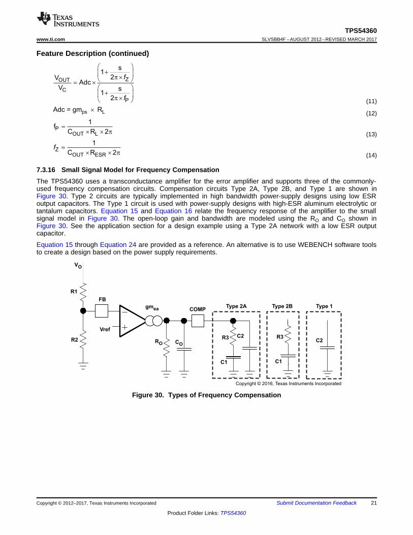
7.3.16 Small Signal Model for Frequency CompensationThe TPS54360 uses a transconductance amplifier for the error amplifier and supports three of the commonly-used frequency compensation circuits. Compensation circuits Type 2A, Type 2B, and Type 1 are shown inFigure 30. Type 2 circuits are typically implemented in high bandwidth power-supply designs using low ESRoutput capacitors. The Type 1 circuit is used with power-supply designs with high-ESR aluminum electrolytic ortantalum capacitors. Equation 15 and Equation 16 relate the frequency response of the amplifier to the smallsignal model in Figure 30. The open-loop gain and bandwidth are modeled using the RO and CO shown inFigure 30. See the application section for a design example using a Type 2A network with a low ESR outputcapacitor.
Equation 15 through Equation 24 are provided as a reference. An alternative is to use WEBENCH software toolsto create a design based on the power supply requirements.
Figure 30. Types of Frequency Compensation

p ´ ´O O
1P2 = type 1
2 R (C2 + C )
p ´ ´O O
1P2 = type 2b
2 R3 | | R C
p ´ ´O O
1P2 = type 2a
2 R3 | | R (C2 + C )
1Z1
2 R3 C1=
p ´ ´
1P1
2 Ro C1=
p ´ ´
ea
R2A1 = gm Ro| | R3
R1 + R2´ ´
ea
R2A0 = gm Ro
R1 + R2´ ´
f
f f
Z1
P1 P2
s1
2EA A0
s s1 1
2 2
æ ö+ç ÷
p ´è ø= ´æ ö æ ö
+ ´ +ç ÷ ç ÷p ´ p ´è ø è ø
p ´
eaO
gmC =
2 BW (Hz)
ea
Aol(V/V)Ro =
gm
A0
A1
P1
Z1 P2
Aol
BW
22
TPS54360SLVSBB4F –AUGUST 2012–REVISED MARCH 2017 www.ti.com
Product Folder Links: TPS54360
Submit Documentation Feedback Copyright © 2012–2017, Texas Instruments Incorporated
Feature Description (continued)
Figure 31. Frequency Response of the Type 2A and Type 2B Frequency Compensation
(15)
(16)
(17)
(18)
(19)
(20)
(21)
(22)
(23)
(24)

SWVIN
GND
BOOT
FB
COMP
TPS54360
EN
RT /CLK
CpoleCzero
Rcomp
RT
Co
Lo
CbootCin
R 1
R 2
Cd
VIN
VOUT
+
+
GND
Copyright © 2017, Texas Instruments Incorporated
23
TPS54360www.ti.com SLVSBB4F –AUGUST 2012–REVISED MARCH 2017
Product Folder Links: TPS54360
Submit Documentation FeedbackCopyright © 2012–2017, Texas Instruments Incorporated
7.4 Device Functional Modes
7.4.1 Operation with VIN = < 4.5 V (Minimum VIN)The device is recommended to operate with input voltages above 4.5 V. The typical VIN UVLO threshold is 4.3 Vand the device may operate at input voltages down to the UVLO voltage. At input voltages below the actualUVLO voltage, the device will not switch. If EN is externally pulled up to VIN or left floating, when VIN passes theUVLO threshold the device will become active. Switching is enabled, and the soft start sequence is initiated. TheTPS54360 will start at the soft start time determined by the internal soft start time.
7.4.2 Operation with EN ControlThe enable threshold voltage is 1.2 V typical. With EN held below that voltage the device is disabled andswitching is inhibited even if VIN is above its UVLO threshold. The IC quiescent current is reduced in this state. Ifthe EN voltage is increased above the threshold while VIN is above its UVLO threshold, the device becomesactive. Switching is enabled, and the soft start sequence is initiated. The TPS54360 will start at the soft start timedetermined by the internal soft start time.
7.4.3 Alternate Power Supply Topologies
7.4.3.1 Inverting PowerThe TPS54360 can be used to convert a positive input voltage to a negative output voltage. Idea applications areamplifiers requiring a negative power supply. For a more detailed example see SLVA317.
Figure 32. TPS54360 Inverting Power Supply

SWVIN
GND
BOOT
FB
COMP
TPS54360
EN
RT /CLK
CpoleCzero
Rcomp
RT
Coneg
Lo
CbootCin
R1
R2
Cd
VIN
VONEG
+
+
GND
VOPOS
Copos+
Copyright © 2017, Texas Instruments Incorporated
24
TPS54360SLVSBB4F –AUGUST 2012–REVISED MARCH 2017 www.ti.com
Product Folder Links: TPS54360
Submit Documentation Feedback Copyright © 2012–2017, Texas Instruments Incorporated
Device Functional Modes (continued)7.4.3.2 Split Rail Power SupplyThe TPS54360 can be used to convert a positive input voltage to a split rail positive and negative output voltageby using a coupled inductor. Idea applications are amplifiers requiring a split rail positive and negative voltagepower supply. For a more detailed example see SLVA369.
Figure 33. TPS54360 Split Rail Power Supply

8.5V to 60V
5.0V, 3.5A
1BOOT
2VIN
3EN
4RT/CLK
5FB
6COMP
7GND
8SW
9
PW
RP
D
U1TPS54360DDA
C5
6800pF
R413.0k C8
39pF
C4 0.1uF
L18.2uH
R6
10.2k
R5
53.6k
R3162k
R1523k
R284.5k
C1
2.2uF
C2
2.2uF
D1
B560C
C6
47uF
C7
47uF
GND
FB
GND
GND
GND
VIN
FB
VOUT
GND
Copyright © 2017, Texas Instruments Incorporated
25
TPS54360www.ti.com SLVSBB4F –AUGUST 2012–REVISED MARCH 2017
Product Folder Links: TPS54360
Submit Documentation FeedbackCopyright © 2012–2017, Texas Instruments Incorporated
8 Application and Implementation
NOTEInformation in the following applications sections is not part of the TI componentspecification, and TI does not warrant its accuracy or completeness. TI’s customers areresponsible for determining suitability of components for their purposes. Customers shouldvalidate and test their design implementation to confirm system functionality.
8.1 Application InformationThe TPS54360 is a 60 V, 3.5 A, step down regulator with an integrated high side MOSFET. Idea applicationsare: 12 V, 24 V and 48 V Industrial, Automotive and Communications Power Systems
8.2 Typical Application
Figure 34. 5 V Output TPS54360 Design Example
8.2.1 Design RequirementsThis guide illustrates the design of a high frequency switching regulator using ceramic output capacitors. A fewparameters must be known in order to start the design process. These requirements are typically determined atthe system level. For this example, start with the following known parameters:
Table 1. Design ParametersParameter Value
Output Voltage 5 VTransient Response 0.875 A to 2.625 A load step ΔVOUT = 4 %Maximum Output Current 3.5 AInput Voltage 12 V nom. 8.5 V to 60 VOutput Voltage Ripple 0.5% of VOUT
Start Input Voltage (rising VIN) 8 VStop Input Voltage (falling VIN) 6.25 V

1.008
101756RT (k ) = = 161 k
600 (kHz)W W
fW + +æ ö
= ´ =ç ÷W +è øSW(shift)
8 4.7 A x 25 m 0.1 V 0.7 V902 kHz
135 ns 60 V - 4.7 A x 92 m 0.7 V
fW + +æ ö
= ´ =ç ÷W +è øSW(max skip)
1 3.5 A x 25 m 5 V 0.7 V710 kHz
135ns 60 V - 3.5 A x 92 m 0.7 V
26
TPS54360SLVSBB4F –AUGUST 2012–REVISED MARCH 2017 www.ti.com
Product Folder Links: TPS54360
Submit Documentation Feedback Copyright © 2012–2017, Texas Instruments Incorporated
8.2.2 Detailed Design Procedure
8.2.2.1 Custom Design with WEBENCH® ToolsClick here to create a custom design using the TPS54360 device with the WEBENCH® Power Designer.1. Start by entering your VIN, VOUT, and IOUT requirements.2. Optimize your design for key parameters like efficiency, footprint and cost using the optimizer dial and
compare this design with other possible solutions from Texas Instruments.3. The WEBENCH Power Designer provides you with a customized schematic along with a list of materials with
real time pricing and component availability.4. In most cases, you will also be able to:
– Run electrical simulations to see important waveforms and circuit performance– Run thermal simulations to understand the thermal performance of your board– Export your customized schematic and layout into popular CAD formats– Print PDF reports for the design, and share your design with colleagues
5. Get more information about WEBENCH tools at www.ti.com/WEBENCH.
8.2.2.2 Selecting the Switching FrequencyThe first step is to choose a switching frequency for the regulator. Typically, the designer uses the highestswitching frequency possible since this produces the smallest solution size. High switching frequency allows forlower value inductors and smaller output capacitors compared to a power supply that switches at a lowerfrequency. The switching frequency that can be selected is limited by the minimum on-time of the internal powerswitch, the input voltage, the output voltage and the frequency foldback protection.
Equation 9 and Equation 10 should be used to calculate the upper limit of the switching frequency for theregulator. Choose the lower value result from the two equations. Switching frequencies higher than these valuesresults in pulse skipping or the lack of overcurrent protection during a short circuit.
The typical minimum on time, tonmin, is 135 ns for the TPS54360. For this example, the output voltage is 5 V andthe maximum input voltage is 60 V, which allows for a maximum switch frequency up to 710 kHz to avoid pulseskipping from Equation 9. To ensure overcurrent runaway is not a concern during short circuits use Equation 10to determine the maximum switching frequency for frequency foldback protection. With a maximum input voltageof 60 V, assuming a diode voltage of 0.7 V, inductor resistance of 25 mΩ, switch resistance of 92 mΩ, a currentlimit value of 4.7 A and short circuit output voltage of 0.1 V, the maximum switching frequency is 902 kHz.
For this design, a lower switching frequency of 600 kHz is chosen to operate comfortably below the calculatedmaximums. To determine the timing resistance for a given switching frequency, use Equation 7 or the curve inFigure 6. The switching frequency is set by resistor R3 shown in Figure 34. For 600 kHz operation, the closeststandard value resistor is 162 kΩ.
(25)
(26)
(27)

( ) = + = + =RIPPLEOUTL peak
I 0.932 AI I 3.5 A 3.97 A
2 2
( ) ( )( )( )
( )( ) ( )
f
æ ö´ - æ ö´ç ÷= + ´ = + ´ =ç ÷ç ÷ ç ÷´ ´ ´ m ´è øç ÷
è ø
22
OUT OUTIN max2 2
OUTL rmsO SWIN max
V V V 5 V 60 V - 5 V1 1I I 3.5 A 3.5 A
12 V L 12 60 V 8.2 H 600 kHz
( )
( ) f
´ -= = =
´ ´ m
OUT OUTIN max
RIPPLEO SWIN max
V (V V ) 5 V x (60 V - 5 V)I 0.932 A
V L 60 V x 8.2 H x 600 kHz
( )( )
( ) f
-= ´ = ´ = m
´ ´ ´
OUTIN max OUT
O minOUT IND SWIN max
V V V 60 V - 5 V 5 VL 7.3 H
I K V 3.5 A x 0.3 60 V 600 kHz
27
TPS54360www.ti.com SLVSBB4F –AUGUST 2012–REVISED MARCH 2017
Product Folder Links: TPS54360
Submit Documentation FeedbackCopyright © 2012–2017, Texas Instruments Incorporated
8.2.2.3 Output Inductor Selection (LO)To calculate the minimum value of the output inductor, use Equation 28.
KIND is a ratio that represents the amount of inductor ripple current relative to the maximum output current. Theinductor ripple current is filtered by the output capacitor. Therefore, choosing high inductor ripple currentsimpacts the selection of the output capacitor since the output capacitor must have a ripple current rating equal toor greater than the inductor ripple current. In general, the inductor ripple value is at the discretion of the designer,however, the following guidelines may be used.
For designs using low ESR output capacitors such as ceramics, a value as high as KIND = 0.3 may be desirable.When using higher ESR output capacitors, KIND = 0.2 yields better results. Since the inductor ripple current ispart of the current mode PWM control system, the inductor ripple current should always be greater than 150 mAfor stable PWM operation. In a wide input voltage regulator, it is best to choose relatively large inductor ripplecurrent. This provides sufficienct ripple current with the input voltage at the minimum.
For this design example, KIND = 0.3 and the minimum inductor value is calculated to be 7.3 μH. The neareststandard value is 8.2 μH. It is important that the RMS current and saturation current ratings of the inductor not beexceeded. The RMS and peak inductor current can be found from Equation 30 and Equation 31. For this design,the RMS inductor current is 3.5 A and the peak inductor current is 3.97 A. The chosen inductor is a WE7447797820, which has a saturation current rating of 5.8 A and an RMS current rating of 5.05 A.
As the equation set demonstrates, lower ripple currents will reduce the output voltage ripple of the regulator butwill require a larger value of inductance. Selecting higher ripple currents will increase the output voltage ripple ofthe regulator but allow for a lower inductance value.
The current flowing through the inductor is the inductor ripple current plus the output current. During power up,faults or transient load conditions, the inductor current can increase above the peak inductor current levelcalculated above. In transient conditions, the inductor current can increase up to the switch current limit of thedevice. For this reason, the most conservative design approach is to choose an inductor with a saturation currentrating equal to or greater than the switch current limit of the TPS54360 which is nominally 5.5 A.
(28)
spacer
(29)
spacer
(30)
spacer
(31)
8.2.2.4 Output CapacitorThere are three primary considerations for selecting the value of the output capacitor. The output capacitordetermines the modulator pole, the output voltage ripple, and how the regulator responds to a large change inload current. The output capacitance needs to be selected based on the most stringent of these three criteria.
The desired response to a large change in the load current is the first criteria. The output capacitor needs tosupply the increased load current until the regulator responds to the load step. The regulator does not respondimmediately to a large, fast increase in the load current such as transitioning from no load to a full load. Theregulator usually needs two or more clock cycles for the control loop to sense the change in output voltage andadjust the peak switch current in response to the higher load. The output capacitance must be large enough to
( )( )( )
( )
f
´ - ´= = =
´ ´ ´ ´ ´ m ´
OUT OUTIN max
COUT(rms)O SWIN max
V V V 5 V 60 V - 5 VI 269 mA
12 V L 12 60 V 8.2 H 600 kHz
< = = WORIPPLE
ESR
RIPPLE
V 25 mVR 27 m
I 0.932 A
f> ´ = = m
´ æ ö æ öç ÷ç ÷è øè ø
OUT
SW ORIPPLE
RIPPLE
1 1 1 1C x 7.8 F
25 mV8 8 x 600 kHzV
0.932 AI
( ) ( )( )( ) ( )( )
( )( )
> = m = m-
2 2 2 2OH OL
OUT O2 2 2 2
f I
I - I 2.625 A - 0.875 A
C L x 8.2 H x 24.6 F
5.2 V 5 VV - V
f
´ D ´> = = m
´ D
OUTOUT
SW OUT
2 I 2 1.75 AC 29.2 F
V 600 kHz x 0.2 V
28
TPS54360SLVSBB4F –AUGUST 2012–REVISED MARCH 2017 www.ti.com
Product Folder Links: TPS54360
Submit Documentation Feedback Copyright © 2012–2017, Texas Instruments Incorporated
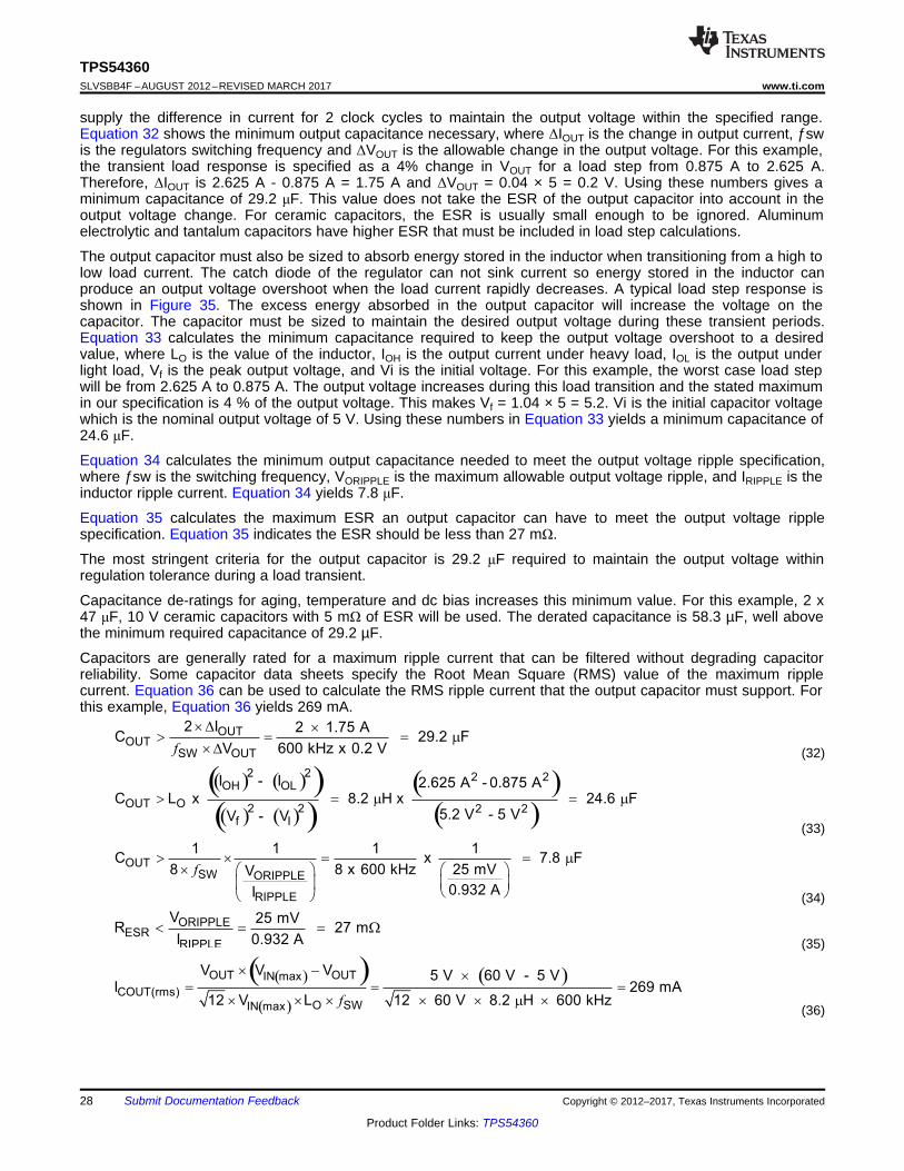
supply the difference in current for 2 clock cycles to maintain the output voltage within the specified range.Equation 32 shows the minimum output capacitance necessary, where ΔIOUT is the change in output current, ƒswis the regulators switching frequency and ΔVOUT is the allowable change in the output voltage. For this example,the transient load response is specified as a 4% change in VOUT for a load step from 0.875 A to 2.625 A.Therefore, ΔIOUT is 2.625 A - 0.875 A = 1.75 A and ΔVOUT = 0.04 × 5 = 0.2 V. Using these numbers gives aminimum capacitance of 29.2 μF. This value does not take the ESR of the output capacitor into account in theoutput voltage change. For ceramic capacitors, the ESR is usually small enough to be ignored. Aluminumelectrolytic and tantalum capacitors have higher ESR that must be included in load step calculations.
The output capacitor must also be sized to absorb energy stored in the inductor when transitioning from a high tolow load current. The catch diode of the regulator can not sink current so energy stored in the inductor canproduce an output voltage overshoot when the load current rapidly decreases. A typical load step response isshown in Figure 35. The excess energy absorbed in the output capacitor will increase the voltage on thecapacitor. The capacitor must be sized to maintain the desired output voltage during these transient periods.Equation 33 calculates the minimum capacitance required to keep the output voltage overshoot to a desiredvalue, where LO is the value of the inductor, IOH is the output current under heavy load, IOL is the output underlight load, Vf is the peak output voltage, and Vi is the initial voltage. For this example, the worst case load stepwill be from 2.625 A to 0.875 A. The output voltage increases during this load transition and the stated maximumin our specification is 4 % of the output voltage. This makes Vf = 1.04 × 5 = 5.2. Vi is the initial capacitor voltagewhich is the nominal output voltage of 5 V. Using these numbers in Equation 33 yields a minimum capacitance of24.6 μF.
Equation 34 calculates the minimum output capacitance needed to meet the output voltage ripple specification,where ƒsw is the switching frequency, VORIPPLE is the maximum allowable output voltage ripple, and IRIPPLE is theinductor ripple current. Equation 34 yields 7.8 μF.
Equation 35 calculates the maximum ESR an output capacitor can have to meet the output voltage ripplespecification. Equation 35 indicates the ESR should be less than 27 mΩ.
The most stringent criteria for the output capacitor is 29.2 μF required to maintain the output voltage withinregulation tolerance during a load transient.
Capacitance de-ratings for aging, temperature and dc bias increases this minimum value. For this example, 2 x47 μF, 10 V ceramic capacitors with 5 mΩ of ESR will be used. The derated capacitance is 58.3 µF, well abovethe minimum required capacitance of 29.2 µF.
Capacitors are generally rated for a maximum ripple current that can be filtered without degrading capacitorreliability. Some capacitor data sheets specify the Root Mean Square (RMS) value of the maximum ripplecurrent. Equation 36 can be used to calculate the RMS ripple current that the output capacitor must support. Forthis example, Equation 36 yields 269 mA.
(32)
(33)
(34)
(35)
(36)

( )( )
( )( )( )
( )-= = ´ =
OUTIN minOUT
OUTCI rms
IN min IN min
V V 8.5 V - 5 VV 5 VI I x x 3.5 A 1.72 A
V V 8.5 V 8.5 V
( )( )( )
( )
( )
f f f- ´ ´ ´ ´ += + =
´ ++ =
2OUT OUTIN max j SW IN
DIN max
2
V V I V d C V V dP
V 2
60 V - 5 V 3.5 A x 0.7 V 300 pF x 600 kHz x (60 V 0.7 V)2.58 W
60 V 2
29
TPS54360www.ti.com SLVSBB4F –AUGUST 2012–REVISED MARCH 2017
Product Folder Links: TPS54360
Submit Documentation FeedbackCopyright © 2012–2017, Texas Instruments Incorporated
8.2.2.5 Catch DiodeThe TPS54360 requires an external catch diode between the SW terminal and GND. The selected diode musthave a reverse voltage rating equal to or greater than VIN(max). The peak current rating of the diode must begreater than the maximum inductor current. Schottky diodes are typically a good choice for the catch diode dueto their low forward voltage. The lower the forward voltage of the diode, the higher the efficiency of the regulator.
Typically, diodes with higher voltage and current ratings have higher forward voltages. A diode with a minimum of60 V reverse voltage is preferred to allow input voltage transients up to the rated voltage of the TPS54360.
For the example design, the B560C-13-F Schottky diode is selected for its lower forward voltage and goodthermal characteristics compared to smaller devices. The typical forward voltage of the B560C-13-F is 0.70 voltsat 5 A.
The diode must also be selected with an appropriate power rating. The diode conducts the output current duringthe off-time of the internal power switch. The off-time of the internal switch is a function of the maximum inputvoltage, the output voltage, and the switching frequency. The output current during the off-time is multiplied bythe forward voltage of the diode to calculate the instantaneous conduction losses of the diode. At higherswitching frequencies, the ac losses of the diode need to be taken into account. The ac losses of the diode aredue to the charging and discharging of the junction capacitance and reverse recovery charge. Equation 37 isused to calculate the total power dissipation, including conduction losses and ac losses of the diode.
The B560C-13-F diode has a junction capacitance of 300 pF. Using Equation 37, the total loss in the diode is2.58 Watts.
If the power supply spends a significant amount of time at light load currents or in sleep mode, consider using adiode which has a low leakage current and slightly higher forward voltage drop.
(37)
8.2.2.6 Input CapacitorThe TPS54360 requires a high quality ceramic type X5R or X7R input decoupling capacitor with at least 3 μF ofeffective capacitance. Some applications will benefit from additional bulk capacitance. The effective capacitanceincludes any loss of capacitance due to dc bias effects. The voltage rating of the input capacitor must be greaterthan the maximum input voltage. The capacitor must also have a ripple current rating greater than the maximuminput current ripple of the TPS54360. The input ripple current can be calculated using Equation 38.
The value of a ceramic capacitor varies significantly with temperature and the dc bias applied to the capacitor.The capacitance variations due to temperature can be minimized by selecting a dielectric material that is morestable over temperature. X5R and X7R ceramic dielectrics are usually selected for switching regulator capacitorsbecause they have a high capacitance to volume ratio and are fairly stable over temperature. The input capacitormust also be selected with consideration for the dc bias. The effective value of a capacitor decreases as the dcbias across a capacitor increases.
For this example design, a ceramic capacitor with at least a 60 V voltage rating is required to support themaximum input voltage. Common standard ceramic capacitor voltage ratings include 4 V, 6.3 V, 10 V, 16 V, 25V, 50 V or 100 V. For this example, two 2.2 μF, 100 V capacitors in parallel are used. Table 2 shows severalchoices of high voltage capacitors.
The input capacitance value determines the input ripple voltage of the regulator. The input voltage ripple can becalculated using Equation 39. Using the design example values, IOUT = 3.5 A, CIN = 4.4 μF, ƒsw = 600 kHz,yields an input voltage ripple of 331 mV and a rms input ripple current of 1.72 A.
(38)
= = = W
+ m+W
ENAUVLO2
START ENA1
UVLO1
V 1.2 VR 84.5 k
V - V 8 V - 1.2 V1.2 AI
523 kR
= = = Wm
START STOPUVLO1
HYS
V - V 8 V - 6.25 VR 515 k
I 3.4 A
f
´ ´D = = =
´ m ´
OUTIN
IN SW
I 0.25 3.5 A 0.25V 331 mV
C 4.4 F 600 kHz
30
TPS54360SLVSBB4F –AUGUST 2012–REVISED MARCH 2017 www.ti.com
Product Folder Links: TPS54360
Submit Documentation Feedback Copyright © 2012–2017, Texas Instruments Incorporated
(39)
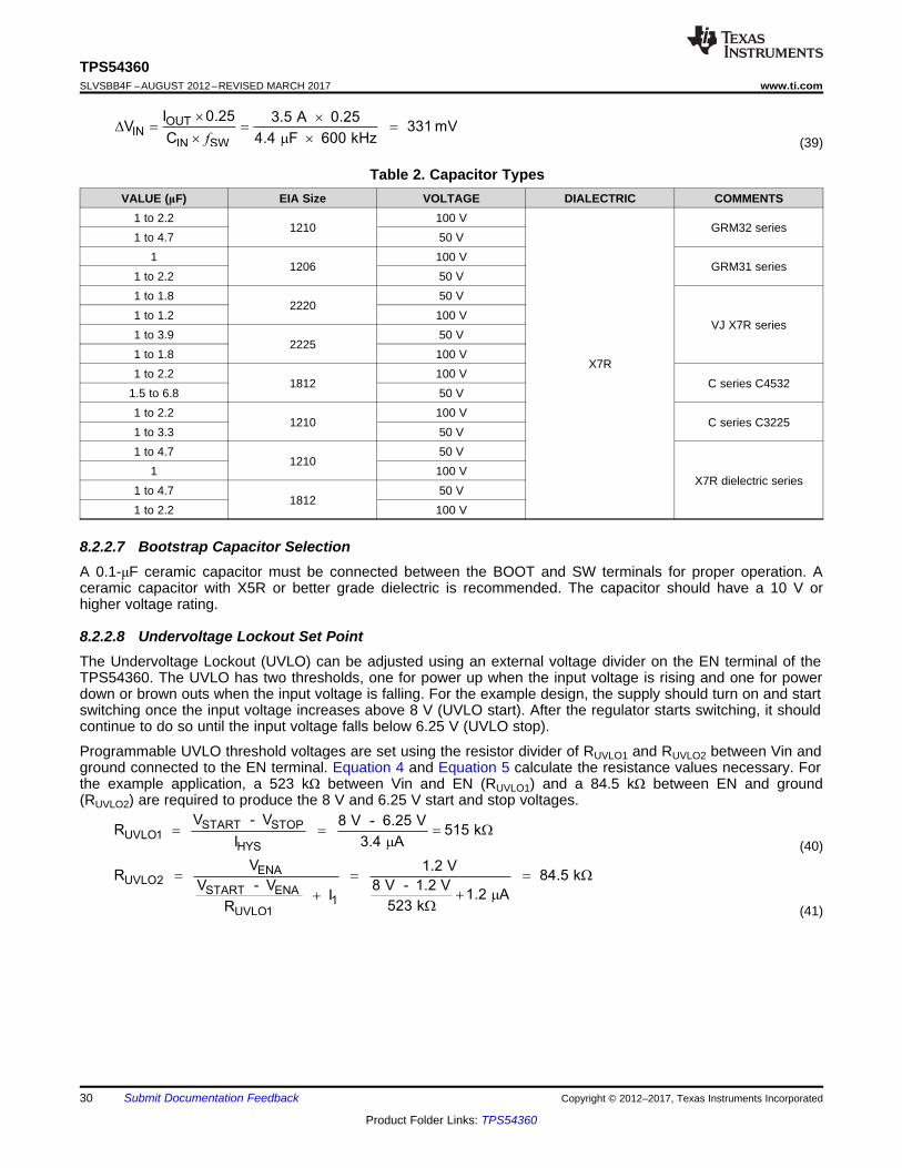
Table 2. Capacitor TypesVALUE (μF) EIA Size VOLTAGE DIALECTRIC COMMENTS
1 to 2.21210
100 V
X7R
GRM32 series1 to 4.7 50 V
11206
100 VGRM31 series
1 to 2.2 50 V1 to 1.8
222050 V
VJ X7R series1 to 1.2 100 V1 to 3.9
222550 V
1 to 1.8 100 V1 to 2.2
1812100 V
C series C45321.5 to 6.8 50 V1 to 2.2
1210100 V
C series C32251 to 3.3 50 V1 to 4.7
121050 V
X7R dielectric series1 100 V
1 to 4.71812
50 V1 to 2.2 100 V
8.2.2.7 Bootstrap Capacitor SelectionA 0.1-μF ceramic capacitor must be connected between the BOOT and SW terminals for proper operation. Aceramic capacitor with X5R or better grade dielectric is recommended. The capacitor should have a 10 V orhigher voltage rating.
8.2.2.8 Undervoltage Lockout Set PointThe Undervoltage Lockout (UVLO) can be adjusted using an external voltage divider on the EN terminal of theTPS54360. The UVLO has two thresholds, one for power up when the input voltage is rising and one for powerdown or brown outs when the input voltage is falling. For the example design, the supply should turn on and startswitching once the input voltage increases above 8 V (UVLO start). After the regulator starts switching, it shouldcontinue to do so until the input voltage falls below 6.25 V (UVLO stop).
Programmable UVLO threshold voltages are set using the resistor divider of RUVLO1 and RUVLO2 between Vin andground connected to the EN terminal. Equation 4 and Equation 5 calculate the resistance values necessary. Forthe example application, a 523 kΩ between Vin and EN (RUVLO1) and a 84.5 kΩ between EN and ground(RUVLO2) are required to produce the 8 V and 6.25 V start and stop voltages.
(40)
(41)

ff f= = =
SWco p(mod) x
600 kHz1912 Hz x 23.9 kHz
2 2
f f f= = =co p(mod) x z(mod) 1912 Hz x 1092 kHz 45.7 kHz
( )f = = =´ p ´ ´ ´ p ´ W ´ mZ mod
ESR OUT
1 11092 kHz
2 R C 2 2.5 m 58.3 F
( )( )
f = = =´ p ´ ´ ´ p ´ ´ m
OUT max
P modOUT OUT
I3.5 A
1912 Hz2 V C 2 5 V 58.3 F
u u
:u :u
OUT F dc OUTIN OUT FDS on
IN
V V R IV min R I V
0.995V 0.5V 0.0253 3.5A
V min 0.12 3.5A 0.5V 5.56V0.99
æ ö= = W = Wç ÷
è ø
OUTHS LS
V - 0.8 V 5 V - 0.8 VR R x 10.2 k x 53.5 k
0.8 V 0.8 V
31
TPS54360www.ti.com SLVSBB4F –AUGUST 2012–REVISED MARCH 2017
Product Folder Links: TPS54360
Submit Documentation FeedbackCopyright © 2012–2017, Texas Instruments Incorporated
8.2.2.9 Output Voltage and Feedback Resistors SelectionThe voltage divider of R5 and R6 sets the output voltage. For the example design, 10.2 kΩ was selected for R6.Using Equation 3, R5 is calculated as 53.5 kΩ. The nearest standard 1% resistor is 53.6 kΩ. Due to the inputcurrent of the FB terminal, the current flowing through the feedback network should be greater than 1 μA tomaintain the output voltage accuracy. This requirement is satisfied if the value of R6 is less than 800 kΩ.Choosing higher resistor values decreases quiescent current and improves efficiency at low output currents butmay also introduce noise immunity problems.
(42)
8.2.2.10 Minimum VIN
To ensure proper operation of the device and to keep the output voltage in regulation, the input voltage at thedevice must be above the value calculated with Equation 43. Using the typical values for the RHS, RDC and VF inthis application example, the minimum input voltage is 5.56 V. The BOOT-SW = 3 V curve in Figure 1 was usedfor RDS(on) = 0.12 Ω because the device operates with low drop out. When operating with low dropout, the BOOT-SW voltage is regulated at a lower voltage because the BOOT-SW capacitor is not refreshed every switchingcycle. In the final application, the values of RDS(on), Rdc and VF used in this equation must include tolerance of thecomponent specifications and the variation of these specifications at their maximum operating temperature in theapplication.
(43)
8.2.2.11 CompensationThere are several methods to design compensation for DC-DC regulators. The method presented here is easy tocalculate and ignores the effects of the slope compensation that is internal to the device. Since the slopecompensation is ignored, the actual crossover frequency will be lower than the crossover frequency used in thecalculations. This method assumes the crossover frequency is between the modulator pole and the ESR zeroand the ESR zero is at least 10 times greater the modulator pole.
To get started, the modulator pole, ƒp(mod), and the ESR zero, ƒz1 must be calculated using Equation 44 andEquation 45. For COUT, use a derated value of 58.3 μF. Use equations Equation 46 and Equation 47 to estimatea starting point for the crossover frequency, ƒco. For the example design, ƒp(mod) is 1912 Hz and ƒz(mod) is 1092kHz. Equation 45 is the geometric mean of the modulator pole and the ESR zero and Equation 47 is the mean ofmodulator pole and the switching frequency. Equation 46 yields 45.7 kHz and Equation 47 gives 23.9 kHz. Usethe lower value of Equation 46 or Equation 47 for an initial crossover frequency. For this example, the target ƒcois 23.9 kHz.
Next, the compensation components are calculated. A resistor in series with a capacitor is used to create acompensating zero. A capacitor in parallel to these two components forms the compensating pole.
(44)
(45)
(46)
(47)
To determine the compensation resistor, R4, use Equation 48. Assume the power stage transconductance,gmps, is 12 A/V. The output voltage, VO, reference voltage, VREF, and amplifier transconductance, gmea, are 5V, 0.8 V and 350 μA/V, respectively. R4 is calculated to be 13 kΩ which is a standard value. Use Equation 49 toset the compensation zero to the modulator pole frequency. Equation 49 yields 6404 pF for compensatingcapacitor C5. 6800 pF is used for this design.

= ´ = ´ m =Q IN QP V I 12 V 146 A 0.0018 W
f= ´ ´ = ´ ´ =GD IN G SWP V Q 12 V 3nC 600 kHz 0.022 W
f= ´ ´ ´ = ´ ´ ´ =SW IN SW OUT riseP V I t 12 V 600 kHz 3.5 A 4.9 ns 0.123 W
( ) ( )æ ö
= ´ ´ = ´ W ´ =ç ÷è ø
2 2OUTCOND OUT DS on
IN
V 5 VP I R 3.5 A 92 m 0.47 W
V 12 V
f= = =
p W p
1 1C8 40.8 pF
R4 x sw x 13 k x 600 kHz x
m W= = =
W
OUT ESRC x R 58.3 F x 2.5 mC8 11.2 pF
R4 13 k
f= = =
´ p ´ ´ p ´ Wp(mod)
1 1C5 6404 pF
2 R4 x 2 13 k x 1912 Hz
f æ ö´ p ´ ´æ ö æ ö´ p ´ ´ mæ ö= = = Wç ÷ç ÷ ç ÷ç ÷ mè ø è øè ø è ø
Fco OUT OUT
REF
2 C V 2 23.9 kHz 58.3 5VR4 x x 13 k
gmps V x gmea 12 A / V 0.8 V x 350 A / V
32
TPS54360SLVSBB4F –AUGUST 2012–REVISED MARCH 2017 www.ti.com
Product Folder Links: TPS54360
Submit Documentation Feedback Copyright © 2012–2017, Texas Instruments Incorporated
(48)
(49)
A compensation pole can be implemented if desired by adding capacitor C8 in parallel with the seriescombination of R4 and C5. Use the larger value calculated from Equation 50 and Equation 51 for C8 to set thecompensation pole. The selected value of C8 is 39 pF for this design example.
(50)
(51)
8.2.2.12 Discontinuous Conduction Mode and Eco-mode BoundaryWith an input voltage of 12 V, the power supply enters discontinuous conduction mode when the output currentis less than 300 mA. The power supply enters Eco-mode when the output current is lower than 24 mA. The inputcurrent draw is 270 μA with no load.
8.2.2.13 Power Dissipation EstimateThe following formulas show how to estimate the TPS54360 power dissipation under continuous conductionmode (CCM) operation. These equations should not be used if the device is operating in discontinuousconduction mode (DCM).
The power dissipation of the IC includes conduction loss (PCOND), switching loss (PSW), gate drive loss (PGD) andsupply current (PQ). Example calculations are shown with the 12 V typical input voltage of the design example.
(52)
spacer(53)
spacer(54)
spacer(55)
Where:
IOUT is the output current (A).
RDS(on) is the on-resistance of the high-side MOSFET (Ω).
VOUT is the output voltage (V).
VIN is the input voltage (V).
ƒsw is the switching frequency (Hz).
trise is the SW terminal voltage rise time and can be estimated by trise = VIN x 0.16ns/V + 3.0ns.
QG is the total gate charge of the internal MOSFET.
IQ is the operating nonswitching supply current.

( ) ( )= - ´TH TOTA max J maxT T R P
= + ´J A TH TOTT T R P
= + + + = + + + =TOT COND SW GD QP P P P P 0.47 W 0.123 W 0.022 W 0.0018 W 0.616 W
33
TPS54360www.ti.com SLVSBB4F –AUGUST 2012–REVISED MARCH 2017
Product Folder Links: TPS54360
Submit Documentation FeedbackCopyright © 2012–2017, Texas Instruments Incorporated
Therefore,(56)
For given TA,
(57)
For given TJMAX = 150°C
(58)
Where:
Ptot is the total device power dissipation (W).
TA is the ambient temperature (°C).
TJ is the junction temperature (°C).
RTH is the thermal resistance of the package (°C/W).
TJMAX is maximum junction temperature (°C).
TAMAX is maximum ambient temperature (°C).
There will be additional power losses in the regulator circuit due to the inductor ac and dc losses, the catch diodeand PCB trace resistance impacting the overall efficiency of the regulator.
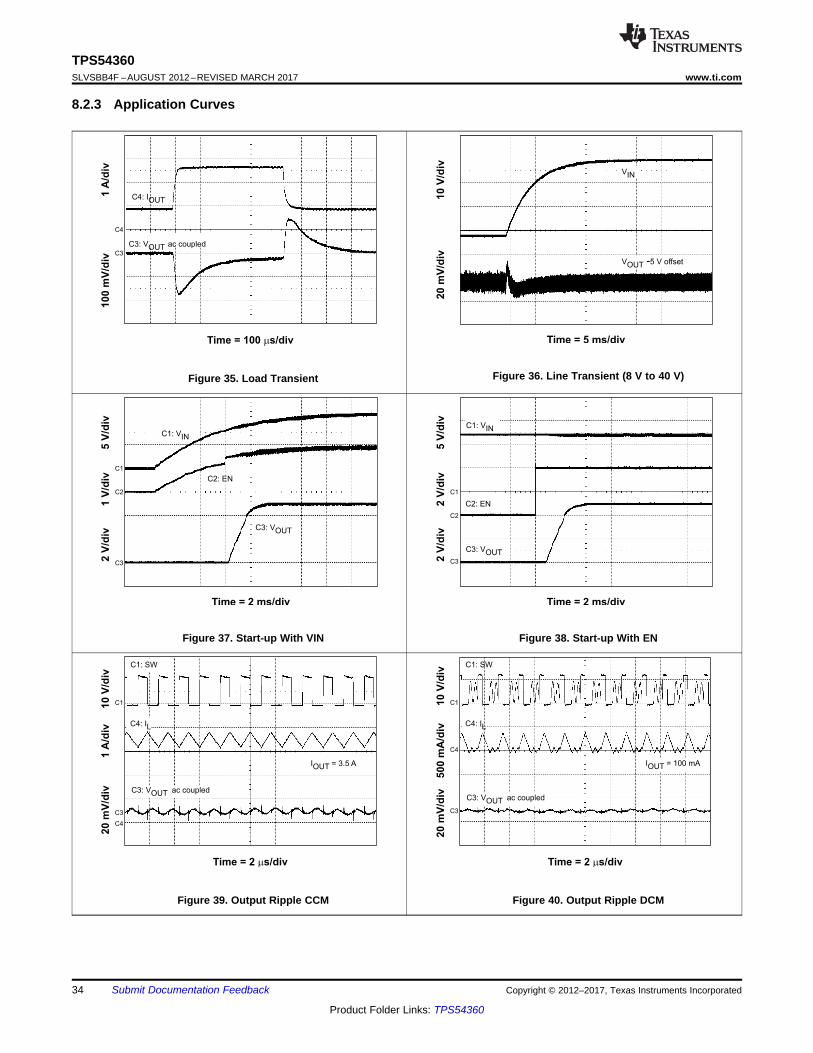
Time = 2 s/divm
1A
/div
10 V
/div
20 m
V/d
iv C3: V ac coupledOUT
C1: SW
C4: IL
I = 3.5 AOUT
C3
C4
C1
Time = 2 s/divm
50
0 m
A/d
iv1
0 V
/div
20
mV
/div C3: V ac coupledOUT
C1: SW
C4: IL
I = 100 mAOUT
C3
C4
C1
Time = 2 ms/div
2 V
/div
5 V
/div
1 V
/div C2: EN
C3: VOUT
C2
C3
C1
C1: VIN
Time = 2 ms/div
2 V
/div
5 V
/div
2 V
/div
C1: VIN
C2: EN
C3: VOUT
C2
C3
C1
Time = 100 s/divm
100 m
V/d
iv
C3: V ac coupledOUT
1A
/div
C4: IOUT
C4
C3
Time = 5 ms/div
20 m
V/d
iv10 V
/div
V 5 V offsetOUT
-
VIN
34
TPS54360SLVSBB4F –AUGUST 2012–REVISED MARCH 2017 www.ti.com
Product Folder Links: TPS54360
Submit Documentation Feedback Copyright © 2012–2017, Texas Instruments Incorporated
8.2.3 Application Curves
Figure 35. Load Transient Figure 36. Line Transient (8 V to 40 V)
Figure 37. Start-up With VIN Figure 38. Start-up With EN
Figure 39. Output Ripple CCM Figure 40. Output Ripple DCM

0
10
20
30
40
50
60
70
80
100
0.001 0.01
I - Output Current - AO
Eff
icie
ncy -
%
0.1
90
1
V = 5V, sw = 600 kHzOUT f
8Vin
12Vin
24Vin
36Vin
48Vin
60Vin0
10
20
30
40
50
60
70
80
100
0 0.5 1.0 1.5 2.0
I - Output Current - AO
Eff
icie
nc
y -
%
2.5 3.0
90
4.03.5
V = 5V, sw = 600 kHzOUT f
8Vin
12Vin
24Vin
36Vin
48Vin
60Vin
Time = 2 s/divm
500 m
A/d
iv10 V
/div
20 m
V/d
iv
C3: V ac coupledIN
C1: SW
C4: IL
I = 100 mAOUT
C3
C4
C1
Time = 20 s/divm
200 m
A/d
iv2 V
/div
20 m
V/d
iv
C3: V ac coupledOUT
C1: SW
C4: IL
No LoadEN Floating
C3
C4
V = 5.5 V
V = 5 VIN
OUT
Time = 2 s/divm
1A
/div
10 V
/div
200 m
V/d
iv
C3: V ac coupledIN
C1: SW
C4: IL
I = 3.5 AOUT
C3
C4
C1
Time = 2 ms/div
200 m
A/d
iv10 V
/div
20 m
V/d
iv
No Load
C1: SW
C4: IL
C3: V ac coupledOUT
C3
C4
C1
35
TPS54360www.ti.com SLVSBB4F –AUGUST 2012–REVISED MARCH 2017
Product Folder Links: TPS54360
Submit Documentation FeedbackCopyright © 2012–2017, Texas Instruments Incorporated
Figure 41. Output Ripple PSM Figure 42. Input Ripple CCM
Figure 43. Input Ripple DCM Figure 44. Low Dropout Operation
Figure 45. Efficiency vs Load Current Figure 46. Light Load Efficiency
-0.5
-0.4
-0.3
0.2
-0.1
0
0.1
0.2
0.3
0.5
0 5 10 15 20
V - Input Voltage - VIN
Ou
tpu
t V
olt
ag
e D
ev
iati
on
- %
25 30
0.4
60
V = 5V,
I = 3.5A
OUT
OUTfsw = 600 kHz,
35 40 45 50 55
-60
-40
-20
0
20
60
10 100
Frequency - Hz
Ga
in -
dB
40
V = 12V,
= 3.5A
IN
OUT
V = 5V,
I
OUT
-180
-120
-60
0
60
120
180
10000 100000 1000000
Ph
as
e -
de
gre
e
1000
Phase
Gain
-1
-0.8
-0.6
0.4
-0.2
0
0.2
0.4
0.6
1
0 0.5 1.0 1.5 2.0
I - Output Current - AO
Ou
tpu
t V
olt
ag
e D
ev
iati
on
- %
2.5 3.0
0.8
3.5
V = 12V,
sw = 600 kHz
IN V = 5V,OUT
f
0
10
20
30
40
50
60
70
80
100
0 0.5 1.0 1.5 2.0
I - Output Current - AO
Eff
icie
nc
y -
%
2.5 3.0
90
4.03.5
8Vin
12Vin
24Vin
36Vin
48Vin
60Vin
V = 3.3V, sw = 300 kHzOUT f
0
10
20
30
40
50
60
70
80
100
0.001 0.01
I - Output Current - AO
Eff
icie
nc
y -
%
0.1
90
1
V = 3.3V, sw = 300 kHzOUT f
8Vin
12Vin
24Vin
36Vin
48Vin
60Vin
36
TPS54360SLVSBB4F –AUGUST 2012–REVISED MARCH 2017 www.ti.com
Product Folder Links: TPS54360
Submit Documentation Feedback Copyright © 2012–2017, Texas Instruments Incorporated
Figure 47. Efficiency vs Load Current Figure 48. Light Load Efficiency
Figure 49. Overall Loop Frequency Response Figure 50. Regulation vs Load Current
Figure 51. Regulation vs Input Voltage
37
TPS54360www.ti.com SLVSBB4F –AUGUST 2012–REVISED MARCH 2017
Product Folder Links: TPS54360
Submit Documentation FeedbackCopyright © 2012–2017, Texas Instruments Incorporated
9 Power Supply RecommendationThe device is designed to operate from an input voltage supply range between 4.5 V and 60 V. This input supplyshould be well regulated. If the input supply is located more than a few inches from the TPS54360 converteradditional bulk capacitance may be required in addition to the ceramic bypass capacitors. An electrolyticcapacitor with a value of 100 μF is a typical choice

BOOT
VIN
EN
RT/CLK
SW
GND
COMP
FB
Input
Bypass
Capacitor
UVLO
Adjust
Resistors
Frequency
Set Resistor
Compensation
NetworkResistor
Divider
Output
Inductor
Output
Capacitor
Vout
Vin
TopsideGround
AreaCatch
Diode
Route Boot CapacitorTrace on another layer toprovide wide path fortopside ground
Thermal VIA
Signal VIA
38
TPS54360SLVSBB4F –AUGUST 2012–REVISED MARCH 2017 www.ti.com
Product Folder Links: TPS54360
Submit Documentation Feedback Copyright © 2012–2017, Texas Instruments Incorporated
10 Layout
10.1 Layout GuidelinesLayout is a critical portion of good power supply design. There are several signal paths that conduct fastchanging currents or voltages that can interact with stray inductance or parasitic capacitance to generate noiseor degrade performance.• To reduce parasitic effects, the VIN terminal should be bypassed to ground with a low ESR ceramic bypass
capacitor with X5R or X7R dielectric.• Care should be taken to minimize the loop area formed by the bypass capacitor connections, the VIN
terminal, and the anode of the catch diode.• The GND terminal should be tied directly to the power pad under the IC and the PowerPAD™.• The PowerPAD™ should be connected to internal PCB ground planes using multiple vias directly under the
IC. The SW terminal should be routed to the cathode of the catch diode and to the output inductor.• Since the SW connection is the switching node, the catch diode and output inductor should be located close
to the SW terminals, and the area of the PCB conductor minimized to prevent excessive capacitive coupling.• For operation at full rated load, the top side ground area must provide adequate heat dissipating area.• The RT/CLK terminal is sensitive to noise so the RT resistor should be located as close as possible to the IC
and routed with minimal lengths of trace.• The additional external components can be placed approximately as shown.• It may be possible to obtain acceptable performance with alternate PCB layouts, however this layout has
been shown to produce good results and is meant as a guideline.
10.2 Layout Example
Figure 52. PCB Layout Example
10.2.1 Estimated Circuit AreaBoxing in the components in the design of Figure 34 the estimated printed circuit board area is 1.025 in2 (661mm2). This area does not include test points or connectors.
39
TPS54360www.ti.com SLVSBB4F –AUGUST 2012–REVISED MARCH 2017
Product Folder Links: TPS54360
Submit Documentation FeedbackCopyright © 2012–2017, Texas Instruments Incorporated
11 Device and Documentation Support
11.1 Documentation Support
11.1.1 Custom Design with WEBENCH® ToolsClick here to create a custom design using the TPS54360 device with the WEBENCH® Power Designer.1. Start by entering your VIN, VOUT, and IOUT requirements.2. Optimize your design for key parameters like efficiency, footprint and cost using the optimizer dial and
compare this design with other possible solutions from Texas Instruments.3. The WEBENCH Power Designer provides you with a customized schematic along with a list of materials with
real time pricing and component availability.4. In most cases, you will also be able to:
– Run electrical simulations to see important waveforms and circuit performance– Run thermal simulations to understand the thermal performance of your board– Export your customized schematic and layout into popular CAD formats– Print PDF reports for the design, and share your design with colleagues
5. Get more information about WEBENCH tools at www.ti.com/WEBENCH.
11.2 Receiving Notification of Documentation UpdatesTo receive notification of documentation updates, navigate to the device product folder on ti.com. In the upperright corner, click on Alert me to register and receive a weekly digest of any product information that haschanged. For change details, review the revision history included in any revised document.
11.3 Community ResourcesThe following links connect to TI community resources. Linked contents are provided "AS IS" by the respectivecontributors. They do not constitute TI specifications and do not necessarily reflect TI's views; see TI's Terms ofUse.
TI E2E™ Online Community TI's Engineer-to-Engineer (E2E) Community. Created to foster collaborationamong engineers. At e2e.ti.com, you can ask questions, share knowledge, explore ideas and helpsolve problems with fellow engineers.
Design Support TI's Design Support Quickly find helpful E2E forums along with design support tools andcontact information for technical support.
11.4 TrademarksEco-mode, PowerPAD, E2E are trademarks of Texas Instruments.WEBENCH is a registered trademark of Texas Instruments.
11.5 Electrostatic Discharge CautionThese devices have limited built-in ESD protection. The leads should be shorted together or the device placed in conductive foamduring storage or handling to prevent electrostatic damage to the MOS gates.
12 Mechanical, Packaging, and Orderable InformationThe following pages include mechanical packaging and orderable information. This information is the mostcurrent data available for the designated devices. This data is subject to change without notice and revision ofthis document. For browser-based versions of this data sheet, refer to the left-hand navigation.
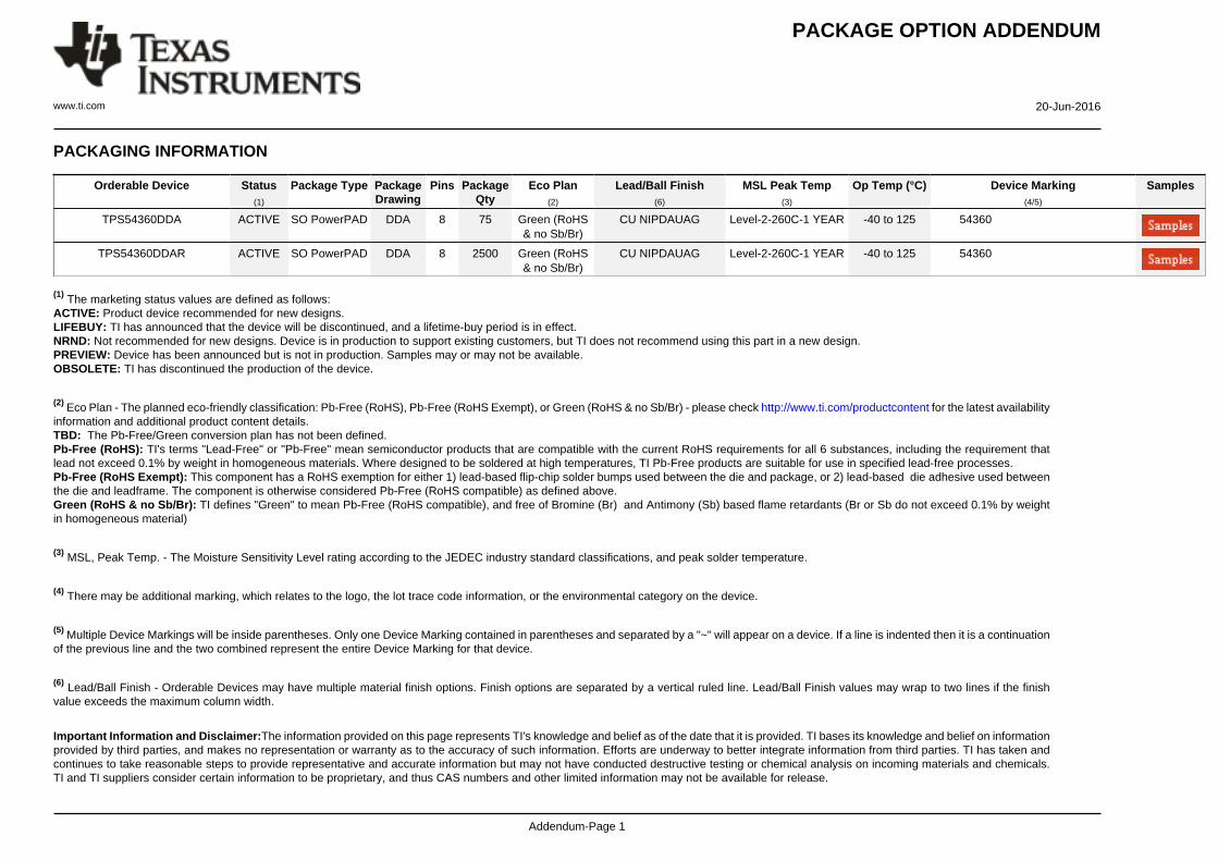
PACKAGE OPTION ADDENDUM
www.ti.com 20-Jun-2016
Addendum-Page 1
PACKAGING INFORMATION
Orderable Device Status(1)
Package Type PackageDrawing
Pins PackageQty
Eco Plan(2)
Lead/Ball Finish(6)
MSL Peak Temp(3)
Op Temp (°C) Device Marking(4/5)
Samples
TPS54360DDA ACTIVE SO PowerPAD DDA 8 75 Green (RoHS& no Sb/Br)
CU NIPDAUAG Level-2-260C-1 YEAR -40 to 125 54360
TPS54360DDAR ACTIVE SO PowerPAD DDA 8 2500 Green (RoHS& no Sb/Br)
CU NIPDAUAG Level-2-260C-1 YEAR -40 to 125 54360
(1) The marketing status values are defined as follows:ACTIVE: Product device recommended for new designs.LIFEBUY: TI has announced that the device will be discontinued, and a lifetime-buy period is in effect.NRND: Not recommended for new designs. Device is in production to support existing customers, but TI does not recommend using this part in a new design.PREVIEW: Device has been announced but is not in production. Samples may or may not be available.OBSOLETE: TI has discontinued the production of the device.
(2) Eco Plan - The planned eco-friendly classification: Pb-Free (RoHS), Pb-Free (RoHS Exempt), or Green (RoHS & no Sb/Br) - please check http://www.ti.com/productcontent for the latest availabilityinformation and additional product content details.TBD: The Pb-Free/Green conversion plan has not been defined.Pb-Free (RoHS): TI's terms "Lead-Free" or "Pb-Free" mean semiconductor products that are compatible with the current RoHS requirements for all 6 substances, including the requirement thatlead not exceed 0.1% by weight in homogeneous materials. Where designed to be soldered at high temperatures, TI Pb-Free products are suitable for use in specified lead-free processes.Pb-Free (RoHS Exempt): This component has a RoHS exemption for either 1) lead-based flip-chip solder bumps used between the die and package, or 2) lead-based die adhesive used betweenthe die and leadframe. The component is otherwise considered Pb-Free (RoHS compatible) as defined above.Green (RoHS & no Sb/Br): TI defines "Green" to mean Pb-Free (RoHS compatible), and free of Bromine (Br) and Antimony (Sb) based flame retardants (Br or Sb do not exceed 0.1% by weightin homogeneous material)
(3) MSL, Peak Temp. - The Moisture Sensitivity Level rating according to the JEDEC industry standard classifications, and peak solder temperature.
(4) There may be additional marking, which relates to the logo, the lot trace code information, or the environmental category on the device.
(5) Multiple Device Markings will be inside parentheses. Only one Device Marking contained in parentheses and separated by a "~" will appear on a device. If a line is indented then it is a continuationof the previous line and the two combined represent the entire Device Marking for that device.
(6) Lead/Ball Finish - Orderable Devices may have multiple material finish options. Finish options are separated by a vertical ruled line. Lead/Ball Finish values may wrap to two lines if the finishvalue exceeds the maximum column width.
Important Information and Disclaimer:The information provided on this page represents TI's knowledge and belief as of the date that it is provided. TI bases its knowledge and belief on informationprovided by third parties, and makes no representation or warranty as to the accuracy of such information. Efforts are underway to better integrate information from third parties. TI has taken andcontinues to take reasonable steps to provide representative and accurate information but may not have conducted destructive testing or chemical analysis on incoming materials and chemicals.TI and TI suppliers consider certain information to be proprietary, and thus CAS numbers and other limited information may not be available for release.

PACKAGE OPTION ADDENDUM
www.ti.com 20-Jun-2016
Addendum-Page 2
In no event shall TI's liability arising out of such information exceed the total purchase price of the TI part(s) at issue in this document sold by TI to Customer on an annual basis.
OTHER QUALIFIED VERSIONS OF TPS54360 :
• Automotive: TPS54360-Q1
NOTE: Qualified Version Definitions:
• Automotive - Q100 devices qualified for high-reliability automotive applications targeting zero defects

TAPE AND REEL INFORMATION
*All dimensions are nominal
Device PackageType
PackageDrawing
Pins SPQ ReelDiameter
(mm)
ReelWidth
W1 (mm)
A0(mm)
B0(mm)
K0(mm)
P1(mm)
W(mm)
Pin1Quadrant
TPS54360DDAR SOPower PAD
DDA 8 2500 330.0 12.8 6.4 5.2 2.1 8.0 12.0 Q1
PACKAGE MATERIALS INFORMATION
www.ti.com 20-Jun-2016
Pack Materials-Page 1

*All dimensions are nominal
Device Package Type Package Drawing Pins SPQ Length (mm) Width (mm) Height (mm)
TPS54360DDAR SO PowerPAD DDA 8 2500 366.0 364.0 50.0
PACKAGE MATERIALS INFORMATION
www.ti.com 20-Jun-2016
Pack Materials-Page 2


IMPORTANT NOTICE
Texas Instruments Incorporated (TI) reserves the right to make corrections, enhancements, improvements and other changes to itssemiconductor products and services per JESD46, latest issue, and to discontinue any product or service per JESD48, latest issue. Buyersshould obtain the latest relevant information before placing orders and should verify that such information is current and complete.TI’s published terms of sale for semiconductor products (http://www.ti.com/sc/docs/stdterms.htm) apply to the sale of packaged integratedcircuit products that TI has qualified and released to market. Additional terms may apply to the use or sale of other types of TI products andservices.Reproduction of significant portions of TI information in TI data sheets is permissible only if reproduction is without alteration and isaccompanied by all associated warranties, conditions, limitations, and notices. TI is not responsible or liable for such reproduceddocumentation. Information of third parties may be subject to additional restrictions. Resale of TI products or services with statementsdifferent from or beyond the parameters stated by TI for that product or service voids all express and any implied warranties for theassociated TI product or service and is an unfair and deceptive business practice. TI is not responsible or liable for any such statements.Buyers and others who are developing systems that incorporate TI products (collectively, “Designers”) understand and agree that Designersremain responsible for using their independent analysis, evaluation and judgment in designing their applications and that Designers havefull and exclusive responsibility to assure the safety of Designers' applications and compliance of their applications (and of all TI productsused in or for Designers’ applications) with all applicable regulations, laws and other applicable requirements. Designer represents that, withrespect to their applications, Designer has all the necessary expertise to create and implement safeguards that (1) anticipate dangerousconsequences of failures, (2) monitor failures and their consequences, and (3) lessen the likelihood of failures that might cause harm andtake appropriate actions. Designer agrees that prior to using or distributing any applications that include TI products, Designer willthoroughly test such applications and the functionality of such TI products as used in such applications.TI’s provision of technical, application or other design advice, quality characterization, reliability data or other services or information,including, but not limited to, reference designs and materials relating to evaluation modules, (collectively, “TI Resources”) are intended toassist designers who are developing applications that incorporate TI products; by downloading, accessing or using TI Resources in anyway, Designer (individually or, if Designer is acting on behalf of a company, Designer’s company) agrees to use any particular TI Resourcesolely for this purpose and subject to the terms of this Notice.TI’s provision of TI Resources does not expand or otherwise alter TI’s applicable published warranties or warranty disclaimers for TIproducts, and no additional obligations or liabilities arise from TI providing such TI Resources. TI reserves the right to make corrections,enhancements, improvements and other changes to its TI Resources. TI has not conducted any testing other than that specificallydescribed in the published documentation for a particular TI Resource.Designer is authorized to use, copy and modify any individual TI Resource only in connection with the development of applications thatinclude the TI product(s) identified in such TI Resource. NO OTHER LICENSE, EXPRESS OR IMPLIED, BY ESTOPPEL OR OTHERWISETO ANY OTHER TI INTELLECTUAL PROPERTY RIGHT, AND NO LICENSE TO ANY TECHNOLOGY OR INTELLECTUAL PROPERTYRIGHT OF TI OR ANY THIRD PARTY IS GRANTED HEREIN, including but not limited to any patent right, copyright, mask work right, orother intellectual property right relating to any combination, machine, or process in which TI products or services are used. Informationregarding or referencing third-party products or services does not constitute a license to use such products or services, or a warranty orendorsement thereof. Use of TI Resources may require a license from a third party under the patents or other intellectual property of thethird party, or a license from TI under the patents or other intellectual property of TI.TI RESOURCES ARE PROVIDED “AS IS” AND WITH ALL FAULTS. TI DISCLAIMS ALL OTHER WARRANTIES ORREPRESENTATIONS, EXPRESS OR IMPLIED, REGARDING RESOURCES OR USE THEREOF, INCLUDING BUT NOT LIMITED TOACCURACY OR COMPLETENESS, TITLE, ANY EPIDEMIC FAILURE WARRANTY AND ANY IMPLIED WARRANTIES OFMERCHANTABILITY, FITNESS FOR A PARTICULAR PURPOSE, AND NON-INFRINGEMENT OF ANY THIRD PARTY INTELLECTUALPROPERTY RIGHTS. TI SHALL NOT BE LIABLE FOR AND SHALL NOT DEFEND OR INDEMNIFY DESIGNER AGAINST ANY CLAIM,INCLUDING BUT NOT LIMITED TO ANY INFRINGEMENT CLAIM THAT RELATES TO OR IS BASED ON ANY COMBINATION OFPRODUCTS EVEN IF DESCRIBED IN TI RESOURCES OR OTHERWISE. IN NO EVENT SHALL TI BE LIABLE FOR ANY ACTUAL,DIRECT, SPECIAL, COLLATERAL, INDIRECT, PUNITIVE, INCIDENTAL, CONSEQUENTIAL OR EXEMPLARY DAMAGES INCONNECTION WITH OR ARISING OUT OF TI RESOURCES OR USE THEREOF, AND REGARDLESS OF WHETHER TI HAS BEENADVISED OF THE POSSIBILITY OF SUCH DAMAGES.Unless TI has explicitly designated an individual product as meeting the requirements of a particular industry standard (e.g., ISO/TS 16949and ISO 26262), TI is not responsible for any failure to meet such industry standard requirements.Where TI specifically promotes products as facilitating functional safety or as compliant with industry functional safety standards, suchproducts are intended to help enable customers to design and create their own applications that meet applicable functional safety standardsand requirements. Using products in an application does not by itself establish any safety features in the application. Designers mustensure compliance with safety-related requirements and standards applicable to their applications. Designer may not use any TI products inlife-critical medical equipment unless authorized officers of the parties have executed a special contract specifically governing such use.Life-critical medical equipment is medical equipment where failure of such equipment would cause serious bodily injury or death (e.g., lifesupport, pacemakers, defibrillators, heart pumps, neurostimulators, and implantables). Such equipment includes, without limitation, allmedical devices identified by the U.S. Food and Drug Administration as Class III devices and equivalent classifications outside the U.S.TI may expressly designate certain products as completing a particular qualification (e.g., Q100, Military Grade, or Enhanced Product).Designers agree that it has the necessary expertise to select the product with the appropriate qualification designation for their applicationsand that proper product selection is at Designers’ own risk. Designers are solely responsible for compliance with all legal and regulatoryrequirements in connection with such selection.Designer will fully indemnify TI and its representatives against any damages, costs, losses, and/or liabilities arising out of Designer’s non-compliance with the terms and provisions of this Notice.
Mailing Address: Texas Instruments, Post Office Box 655303, Dallas, Texas 75265Copyright © 2017, Texas Instruments Incorporated