Embed Size (px)
Citation preview

6. Scanning Electron Microscopy (SEM) Literature: „Rasterelektronenmikroskopie“ L. Reimer und G. Pfefferkorn, Springer Verlag, Berlin 1973 „Praxis der Rasterelektronenmikroskopie und Mikrobereichanalyse“ Peter F. Schmidt, expert verlag, Renningen-Malmsheim 1994

6.1 Introduction
• History – First electron microscope in the 1930ies by Knoll and Ruska
(transmission geometry) – First SEM in UK in the 40ies
• Properties – Big depth of focus – “Three-dimensional” image vie shadow effects – Resolution
• Priniple: – Electron beam scans surface – Image recorded pixel by pixel

• Signels for imaging

6.2 Wave-Particle Dualism of Electrons
• de Broglie Beziehung, Wellenlänge eines Teilchens:
m Masse, v Geschwindigkeit des Elektrons, p Impuls • Energie des Elektrons
U Beschleunigungsspannung • Wellenlänge
• mit relativistischer Korrektur
mo Ruhemasse des Elektrons
• Wellenlänge 0.012 nm bei 10 kV und 0.0037 nm bei 100kV
mvh
ph==λ
eU2mv2
=
meU2h
=λ
⎟⎟
⎠
⎞
⎜⎜
⎝
⎛
⎟⎟
⎠
⎞
⎜⎜
⎝
⎛+
=λ
2o
ocm2
eU1eUm2
h

6.3 Interaction between electrons and specimen • Formation of a “diffusion cloud” by elastic and inelastic scattering ot the primary
electrons (PE) in the solid
• Diameter of cloud >> diameter of beam
• Penetration depth x and diameter of cloud is function of – Acceleration voltage (U↑ x ↑)
– Specimen material (Z↑ x↓)
• Conductive specimen required

• Elastic scattering – Coulomb interaction – High scattering angles – No energy loss – Back scattered electrons; energy: 50 eV … U(PE)
• inelastic scattering – Electron-electron-interaction – Loss of kinetic energy by
• Ionization of atoms by electron loss from core level • Electron from outer shells are moved to unoccupied states (Energy bands) • Often energy loss by small amounts 5-50 eV • Secondary elecrons created in depth of 1-10 nm
N(E)

6.4 Setup of SEM
Components – Colum and Vakuum Chamber – Electron gun – Electron optics – Stage – Detectors (SE, BSE, X-Ray) – Recording (Screen, Film,
Computer)

• Thermionic (hot) cathode (W, LaB6) – Gun heated (2500-3000 K für W) – Electrons are emitted into vacuum; accelerated by high tension (1-50 kV) – Current density ca. 5 A/cm2 – Life cycle of cathode (limited by evaporation) (10 bis 150 h) – Vacuum required because of oxidation of W – Workfunction of LaB6 lower à lower T (1500-2000 K),higher current density (50 A/cm2), higher life time
• Field emission guns – Cathode material W – 1. Anode creates high electric field à tunneling effect – 2. Anode accelerate electrons – UHV required – Cold emission possible; hot mostly used in technology – Current densitys ca. 106 A/cm2
Electron beam formation / Electron gun

• Comparison of the different guns: CFE cold field emission - TFE thermal field emission
Eelectron guns

• Forms a smaller image of cathode on specimen surface
• Electro-magnetic lenses, deflection vie Lorentz-force, cork screw shaped movement
• Scanning unit
• Magnification V:
• Adjustable focus length by objective lens current
• Beam spread angle < 1°, Rayleigh-resolution ca. 60λ
• Field of depth higher in comparison to optical microscope
Electron optic
•V =Size monitor
Size of scanned area


• Aberrations – Spherical Aberration – Chromatic Aberration (energy spread) – Astigmatism
Bsp.: Astigmatismus
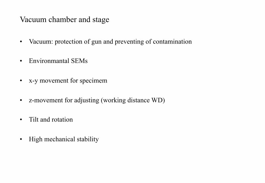
Vacuum chamber and stage • Vacuum: protection of gun and preventing of contamination
• Environmantal SEMs
• x-y movement for specimem
• z-movement for adjusting (working distance WD)
• Tilt and rotation
• High mechanical stability

• Photo-multiplier – SE mit Saugspannung – RE möglich, mit Gegenspannung zur Ablenkung der SE
• Semiconductor (only BSE)
• Robinson-Detector (BSE)
Detectors

6.5 Imaging with SE and BSE • Image formation governed by yields:
– BSE, back scatter coefficient:
function of • Material (change and increasing with Z) • Angle of incident • Crystal orientation
– SE:
function of • Plane inclination • Edges • Material (higher for lower Z)
• Interpretation of image: Analogue to diffuse scattered light – Detector resemble light source – Inclined planes “look” brighter
• Shadowing because of geometry
PEREnn
=η
PESEnn
=δ
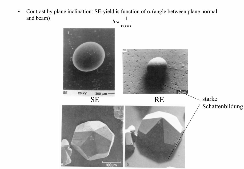
SE RE
• Contrast by plane inclination: SE-yield is function of α (angle between plane normal and beam)
α∝δcos1
starke Schattenbildung
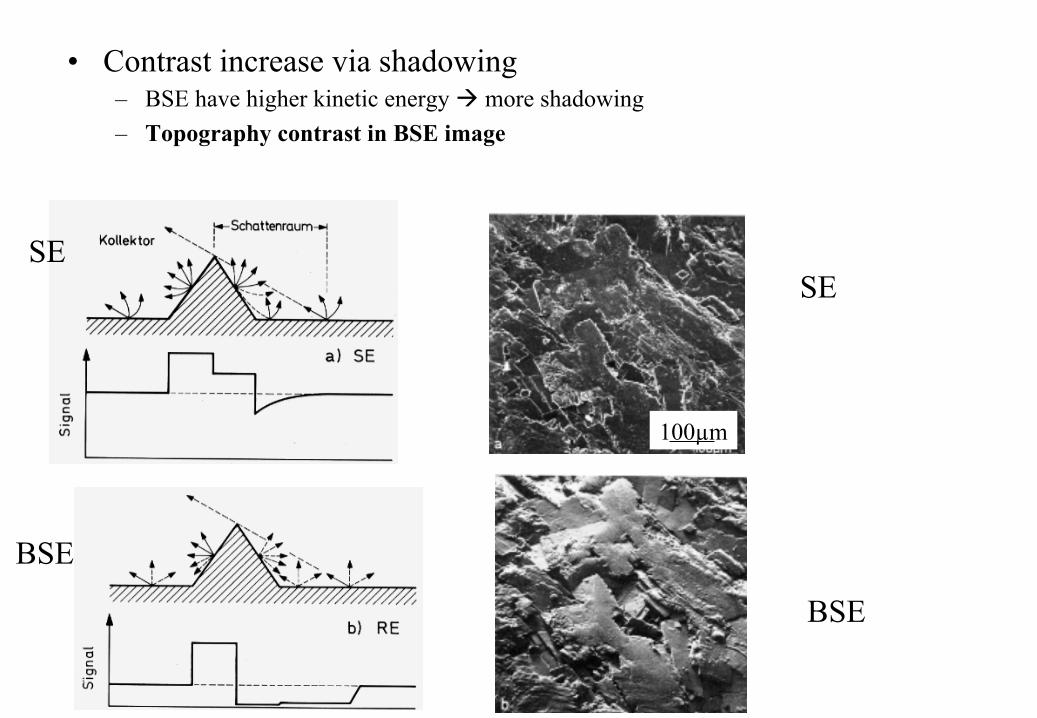
• Contrast increase via shadowing – BSE have higher kinetic energy à more shadowing – Topography contrast in BSE image
SE SE
BSE
BSE
100µm

• Edge effects – Stronger SE- (and BSE-Signal) at edges due to higher electron emission – à edges often brighter – Small edges: only SE effect, not seen by BSE – à high magnification: SE images are “better”
Detektor

• Topography and Materilas contrast – BSE-Image: sensitive on material
RE BSE

• Resolution – SEM: Diameter of electron beam – Dependent on current density – à FEG:
• High current density, small electron source • Low voltage possible
– Diameter of diffusion cloud! ! SE better then BSE!!!

• Auflösung am Beispiel von Au-Inseln auf Graphit
BSE SE

• Charging !!
Reichweite der PE ≈ Austrittstiefe der SE
Cu σ=δ+η

• Channeling- or Orientation contrast – PE parallel to crystal planes -> higher penetration depth ➠ channeling – Lower BSE- and SE-yield – (only seen on almost perfect surfaces)
6.6 Electron-Channeling
RE
RE

• Electron-Channeling-Pattern (ECP)
– Channeling-Effect for determination of: • Lattice • Orientation of known lattice
– Elektronenstrahl überstreicht mit großem Winkel einen einkristallinen Bereich (Standardverfahren, mehrere mm große Probe erforderlich)
– Alternativ: Elektronenstrahl wird auf einen Punkt fixiert und hin- und hergeschwenkt (Feinbereichsmethode, lateraler Auflösung von etwa 2 µm)
– Elektronenbeugung führt zu ECP, die charakteristisch für Kristallgitter und seine Orientierung sind


• Electron-Channeling-Pattern (ECP)
example: Si-Einkristall
Zonenachse: Richtung [uvw], der mehrere Ebenen {hkl} angehören. Zonengleichung: uh+vk+wl=0

• Electron beam stable at one position (no tilt as in ECP) • Distribution of BSE on CCD • Electron diffraction leads to Kikuchi-Lines • Indexing of crystal orientation • Automatic recoring via software • Lateral resolution 20 -200 nm • Time per pixel: 1-10 s
6.6 Electron-Back-Scatter-Patterning (EBSP oder EBSD)
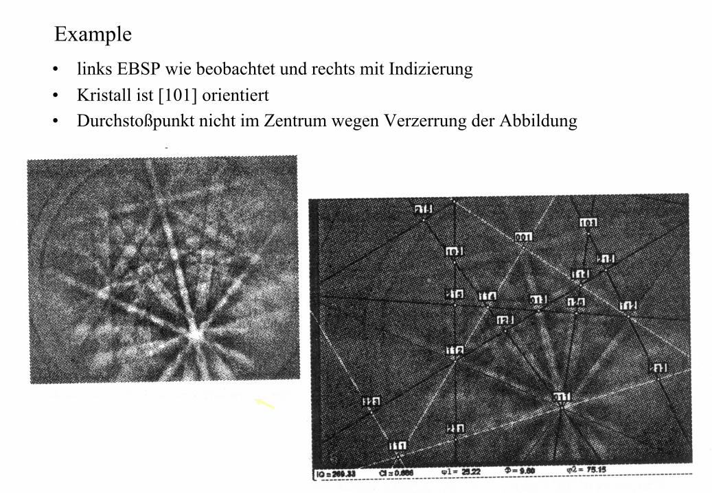
• links EBSP wie beobachtet und rechts mit Indizierung • Kristall ist [101] orientiert • Durchstoßpunkt nicht im Zentrum wegen Verzerrung der Abbildung
Example

links: Bild mit Channeling-Kontrast rechts: zugehörige EBSP-Auswertung (markiertes (blaues) Korn hat [100]-
Orientierung, andere graue (rote) Körner [111]-Orientierung, restliche sind weiß)
[110]
[010]
beam axis
3 µm

oben: Bild mit Channeling-Kontrast unten: EBSP-Auswertung der gleiche Stelle zur Bestimmung der
Korngrenzeigenschaften (Kleinwinkel- und Zwillingskorngrenzen: dicke Linien; Großwinkelkorngrenzen: dünne Linien)

Au/NaCl(100): Cube-on-cube orientation relation
SEM EBSD
NaCl (100) Au (100)
500 nm Au on NaCl