Embed Size (px)
Citation preview

6-k 43-Gb/s Differential Transimpedance-Limiting
Amplifiers with Auto-zero Feedback and High Dynamic
Range
H. Tran1, F. Pera2, D.S. McPherson1, D. Viorel1, and S.P. Voinigescu3
1) Quake Technologies, Inc. Ottawa, ON, K2K 2T8, Canada2) now with Insyte Corporation, Ottawa, ON, K2K 3C9, Canada3) ECE Dept., University of Toronto, Toronto, ON, M5S 3G4, Canada

Wednesday, November 12, 2003 Slide 2M3
OutlineOutline
OverviewOverview
Broadband low-noise amplifier topologies and design Broadband low-noise amplifier topologies and design
methodology methodology
Circuit design and featuresCircuit design and features
Measurement resultsMeasurement results
SummarySummary

Wednesday, November 12, 2003 Slide 3M3
Low-noise broadband amplifier topologyLow-noise broadband amplifier topology
GoalsGoals
Minimize noise when circuit operated as Minimize noise when circuit operated as
TIA with 60-fF photodiode andTIA with 60-fF photodiode and
As 50-As 50- voltage preamplifier voltage preamplifier
Maximise dynamic range by using on-chip active Maximise dynamic range by using on-chip active
feedback that feedback that does not degradedoes not degrade overall noise. overall noise.

Wednesday, November 12, 2003 Slide 4M3
Low-noise broadband topology choicesLow-noise broadband topology choices
EF-input stages have series feedback EF-input stages have series feedback
which increases noise impedance and which increases noise impedance and
results in very high noise figure.results in very high noise figure.
EF+INV or EF+INV or EF+Cherry-Hooper EF+Cherry-Hooper
Inverter Inverter
Differential TIA Differential TIA

Wednesday, November 12, 2003 Slide 5M3
Noise figure topology analysisNoise figure topology analysis
Diff. INVDiff. INV stage with on-chip 50 stage with on-chip 50 resistorsresistorshas low-to-has low-to-
moderate noise but poor broadband Smoderate noise but poor broadband S1111
F(ZF(Z00 = 50 = 50 ) = 1 + [1 + () = 1 + [1 + (LLFF/Z/Z00))22]]-1-1 + G + GntntZZ00 + R + RntntZZ00(Y(Ycortcort + 2/Z + 2/Z00))22
where: where: GGnt nt = G = G 22LLEOPTEOPT, Y, Ycortcort = jB = jBLLEOPTEOPT and R and Rnt nt = R/L= R/LEOPTEOPT
Diff. TIADiff. TIA stage matched to 50 stage matched to 50 offers lowest noise and offers lowest noise and
broadband Sbroadband S1111 matching matching
F(ZF(Z00) = 1 + (Z) = 1 + (Z00/R/RFF)[1+()[1+(LLFF/R/RFF))22]]-1-1 + G + GntntZZ00 + R + RntntZZ00(Y(Ycortcort + 1/Z + 1/Z0 0 +1/R+1/RFF ) )22
If RIf RFF=Z=Z00 the two stages have identical Noise Figure. the two stages have identical Noise Figure.

Wednesday, November 12, 2003 Slide 6M3
Transistor sizing for noise impedanceTransistor sizing for noise impedance
Inverter input stage with matching 50-Inverter input stage with matching 50-resistorsresistorshas has
moderate transistor size (lmoderate transistor size (lEOPTEOPT) and bias current.) and bias current.
llEOPTEOPT = [2/( = [2/(ZZ00)][R/(G + RB)][R/(G + RB22)])]1/21/2
TIA stage matched to 50 TIA stage matched to 50 offers lowest size offers lowest size
(since R(since RFF > Z > Z
00) and bias current.) and bias current.
llEOPTEOPT = (1/ = (1/RRFFZZ00)][R/(G + RB)][R/(G + RB22)])]1/21/2
where R, G, B are technology-specific noise parameterswhere R, G, B are technology-specific noise parameters

Wednesday, November 12, 2003 Slide 7M3
TIALA specificationsTIALA specifications
200 .. 400 mVp-p per sideAdjustable output amplitude
Adjustable input slicing level
Signal level monitor
50 On-chip terminated outputs
450 mWDC power dissipation
3.3 VSingle-supply
ppto mA
ppDynamic range (BER<10-1
6 k(40 dB)Differential Tz/(power) gain

Wednesday, November 12, 2003 Slide 8M3
TIALA block diagramTIALA block diagram

Wednesday, November 12, 2003 Slide 9M3
TIA stage schematicsTIA stage schematics

Wednesday, November 12, 2003 Slide 10M3
Peak detector and output stagePeak detector and output stage

Wednesday, November 12, 2003 Slide 11M3
DC auto-zero feedback stageDC auto-zero feedback stage

Wednesday, November 12, 2003 Slide 12M3
Chip microphotographChip microphotograph
Fabricated by HRL-Fabricated by HRL-LaboratoriesLaboratories
1 1 m, 160-GHz InP/InGaAs m, 160-GHz InP/InGaAs
HBT process HBT process
Substrate height of 100 Substrate height of 100 mm
Two metal layersTwo metal layers
MIM capacitorsMIM capacitors
Metal resistorsMetal resistors
70-70- CPWs for isolation CPWs for isolation
1.8 mm1
mm

Wednesday, November 12, 2003 Slide 13M3
On-wafer DC output offset measurementsOn-wafer DC output offset measurements
Output differential DC-Output differential DC-
offset less than 40 mVoffset less than 40 mVpppp
for entire range of input for entire range of input
DC currentDC current

Wednesday, November 12, 2003 Slide 14M3
On-wafer S-parameter measurementsOn-wafer S-parameter measurements
TIA BWTIA BW3dB3dB 38 GHz38 GHz
TIA TTIA Tzz gaingain 540 540
TIALA BWTIALA BW3dB3dB 36 GHz36 GHz
TIALA STIALA S2121 40 dB40 dB
Isolation Isolation > 50 dB> 50 dB
SS1111 < -15 up to 50 < -15 up to 50
GHzGHz
SS2222 < -10 up to 50 < -10 up to 50 GHzGHz
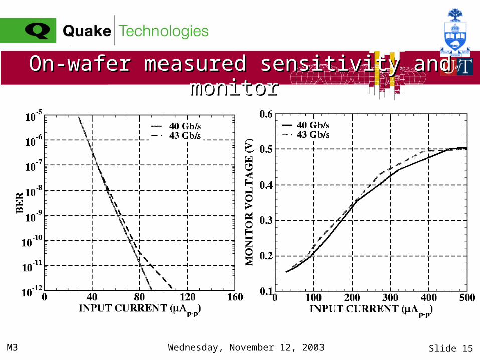
Wednesday, November 12, 2003 Slide 15M3
On-wafer measured sensitivity and monitor On-wafer measured sensitivity and monitor

Wednesday, November 12, 2003 Slide 16M3
On-wafer 43-Gb/s eye-diagramsOn-wafer 43-Gb/s eye-diagrams
43-Gb/s, 231-1 differential output eye-diagram with 4.5-mApp input.
43-Gb/s, 231-1 differential output eye-diagram with 250-A
ppinput.

Wednesday, November 12, 2003 Slide 17M3
As 43-Gb/s Limiting Amplifier in Module As 43-Gb/s Limiting Amplifier in Module
43-Gb/s, 231-1 input eye-diagram with 8-mV
pp input signal level.
Error-free 43-Gb/s, 231-1 output eye-diagram with 8-mV
pp input signal level
and 300-mVpp output swing.
Wednesday, November 12, 2003 Slide 18M3
SummarySummary
A high dynamic range TIALA with on-chip auto-zero feedback A high dynamic range TIALA with on-chip auto-zero feedback was designed and fabricated in InP/InGaAs HBT technologywas designed and fabricated in InP/InGaAs HBT technology
The input stage topology and design were optimized for The input stage topology and design were optimized for
broadband noise and input-impedance matchingbroadband noise and input-impedance matching
Signal monitor and slicing level adjust functions are Signal monitor and slicing level adjust functions are
incorporatedincorporated
The result is a unique circuit, with record functionality, that The result is a unique circuit, with record functionality, that
also operates as a 43-Gb/s, 50-also operates as a 43-Gb/s, 50- matched voltage preamp or matched voltage preamp or
LA with record-breaking 8-mVLA with record-breaking 8-mVpppp sensitivity sensitivity

Wednesday, November 12, 2003 Slide 19M3
AcknowledgmentAcknowledgment
The authors would like to thank HRL-Laboratories for The authors would like to thank HRL-Laboratories for fabricating the diefabricating the die
They would also like to express their gratitude to Quake They would also like to express their gratitude to Quake colleagues M. Tazlauanu and S. Szilagyi for their colleagues M. Tazlauanu and S. Szilagyi for their valuable contributionsvaluable contributions

Wednesday, November 12, 2003 Slide 20M3
Limiting stage schematicsLimiting stage schematics
Wednesday, November 12, 2003 Slide 21M3
Design overviewDesign overview
On-chip auto-zero feedback for increased dynamic rangeOn-chip auto-zero feedback for increased dynamic range
Simultaneous noise- and input-impedance matchingSimultaneous noise- and input-impedance matching
TIA and 2nd. gain stage operate in linear modeTIA and 2nd. gain stage operate in linear mode
Output stages operate in limiting modeOutput stages operate in limiting mode
Signal level monitor, slicing level adjust, and output Signal level monitor, slicing level adjust, and output
swing control functionsswing control functions
Based on a 1-Based on a 1-m InP/InGaAs technologym InP/InGaAs technology

Wednesday, November 12, 2003 Slide 22M3
TIA stage design methodologyTIA stage design methodology
Transistors biased @ 0.6 mA/Transistors biased @ 0.6 mA/mm22 for minimum noise for minimum noise figure at 36 GHz, not for maximum gain/bandwidthfigure at 36 GHz, not for maximum gain/bandwidth
Transistors sized such that the optimal noise impedance Transistors sized such that the optimal noise impedance
with feedback is close to 50 with feedback is close to 50
Inductors deployed in feedback network rather than in Inductors deployed in feedback network rather than in
series with the loads for: series with the loads for:
improving Simproving S1111 over broader bandwidth, over broader bandwidth,
3-dB bandwidth extension, and HF noise filtering.3-dB bandwidth extension, and HF noise filtering.
Wednesday, November 12, 2003 Slide 23M3
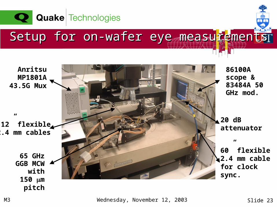
Setup for on-wafer eye measurementsSetup for on-wafer eye measurements
AnritsuMP1801A
43.5G Mux
86100A scope & 83484A 50 GHz mod.
12” flexible2.4 mm cables
65 GHz GGB MCW with
150 m pitch
20 dBattenuator
60” flexible2.4 mm cablefor clocksync.

Wednesday, November 12, 2003 Slide 24M3
Bandwidth of measurement setupBandwidth of measurement setup
BW = 16 GHz

Wednesday, November 12, 2003 Slide 25M3
40 Gb/s eye-diagram (test setup)40 Gb/s eye-diagram (test setup)
• Tr = 12.7 ps• Tf = 11.9 ps• Tj = 6.7 ps


![plaY [pera]](https://img.pdfslide.us/doc/110x75/58eba4601a28ab1b5d8b45b9/play-pera.jpg)