Embed Size (px)
Citation preview
SAND96-0516 Distribution Unlimited Release Category UC-404
Printed March 1996
Diamond and Diamond-Like Carbon Films for Advanced Electronic Applications
M. P. Siegal, T. A. Friedmann, J. P. Sullivan, J. Mikkalson and F. Dominguez Advanced Materials Physics and Devices Department
S. R. Kurtz Photonics Research Department
D. R. Tallant and R. L. Simpson SurfacelMolecular Spectro/Gas Department
Sandia National Laboratories 5Cl...-J i ~ Albuquerque, NM 87185
K. F. McCarty, L Bemardez, D. Dibble and P. B. Mirkarimi Advanced Materials Research Department
JSandia National Laboratories d. ,. L e. ..' fA..CY ~ so-"~ f ......... f ' ~
Livennore, CA 94551
Abstract
The aim of this laboratory-directed research and development (LORD) project was to develop diamond and/or diamond-like carbon (DLC) films for electronic applications. In general, the quality of diamond and DLC films grown by chemical vapor deposition (CVD) is not adequate for electronic applications. Nucleation of diamond grains during growth typically results in coarse films that must be very thick in order to be physically continuous. DLC films grown by CVD are heavily hydrogenated and are stable to temperatures ~ 40(tC. However, diamond and DLC's exceptional electronic properties make them candidates for integration into a variety of microelectronic structures. This work has studied new techniques for the growth of both materials. Template layers have been developed for the growth of CVD diamond films resulting in a significantly higher nucleation density on unscratched or unprepared Si surfaces. Hydrogenfree DLC with temperature stability ~ 800·C has been developed using energetic growth methods such as high-energy pulsed-laser deposition. The applications with the largest system impact include electron-emitting materials for flat-panel displays, dielectrics for interconnects, diffusion barriers, encapsulants, and nonvolatile memories, and tribological coatings that reduce wear and friction in integrated micro-electro-mechanical devices.

Acknowledgment
The authors thank N. Missert of the Advanced Materials Physics and Devices Department and P. P. Newcomer of the Nanostructures and Advanced Materials Chemistry Department for helpful discussions and assistance with electron microscopy. We thank C. A. Apblett of the Films and Operations Department for providing metallized Si substrates for a-tC film deposition and many useful conversations about dielectric properties. We thank M. L. Lovejoy of the Advanced Devices and Applications Department for assistance with microfabrication of test structures for electrical characterization. In addition, we thank L. J. Martinez-Miranda of the University of Maryland for performing x-ray scattering measurements on a-tC films at the synchrotron facility at Brookhaven National Laboratory. Finally, we thank N. J. DiNardo and T. W. Mercer of Drexel University for AFM and STM analysis.
The overall knowledge base developed in this LDRD project gained relevance due to important collaborations with other Sandia programs. These include electron emission characterization by T. Felter and A. Talin of the Physical Properties of Materials Department, and collaborations with CRADA partners at Du Pont (D. Coates, W. Holstein, I. Shah and C. Fincher) and Motorola (J. Jaskie, Y. Kato, E. Menu, J. Song and B. ColI).
Finally, we would like to thank our 1995 summer student, Steven Fleming (Rice University, 1995) for assistance in the laboratory growing films, measuring electrical properties, and preparing samples for TEM.
ii

Contents
I. Introduction..........................................................................................................................1
ll. Diamond Deposition on Polycrystalline Films of Cubic Boron Nitride ..............................3
m. Experimental Results from Attempted CVD Growth of Diamond on a-tC .........................9
IV. Growth and Characterization of a-tC by Pulsed Laser Deposition in High Vacuum ..........9
V. a-tC Thin Films Grown by PLO in Various Gas Ambients ..............................................17
VI. Thermal Stability of a-tC Films Grown by PLO ...............................................................22
Vll. Evaluation of a-tC and BN Films as Low Permittivity Dielectrics ...................................27
VIll. Ion-Assisted Pulsed Laser Deposition of a-tC Films .........................................................32
IX. Summary ...........................................................................................................................39
Figures
2.1 FTIR spectra. of c-BN films ................................................................................................4 2.2 Raman spectra. for diamond on c-BN ..................................................................................5 2.3 FTIR of c-BN before and after diamond deposition ...........................................................6 2.4 SEM of diamond grown on c-BN .......................................................................................7 2.5 SEM of diamond on c-BN and Si .......................................................................................7
4.1 PLO chamber diagram ...................................................................................................... 1 0 4.2 Raman spectra. for five different forms of carbon ............................................................. 11 4.3 a-tC film residual stress vs. PLO energy density ..............................................................12 4.4 Raman for a-tC grown at different PWenergy densities .................................................13 4.5 In-situ Raman of a-tC at elevated temperatures in argon ..................................................14 4.6 I-V characteristic of a Si(p-type)/a-tClHg structure ..........................................................14 4.7 C-V data on a Si(p-type)/a-tCfHg structure for different modulation frequencies ............ 15
5.1 Film stress vs. pressure for a-tC grown in an Ar ambient ...........................................18 5.2 Film stress vs. pressure for a-tC grown in hydrogen or nitrogen ambients ......................18 5.3 Raman spectra. for a-tC grown in Ar, H2, and N2 ambients .............................................20
6.1 Raman spectra. for a-tC as-grown and annealed (500·C in vacuum) .................................23 6.2 Thermal stability of a-tC grown in vacuum or N 2 by Raman ...........................................24
iii

7.1 Dielectric constants for a-tC grown in vacuum and H2 vs. PLD energy density ..............29 7.2 Histogram of dielectric constants for a-tC MIM and MIS diodes ....................................29
8.1 Diagram of ion-assisted pulsed-laser deposition chamber ................................................33 8.2 Deconvolution of an a-tC Raman spectra with a two gaussian fit ....................................34 8.3 Raman intensity of a-tC as a function of ion beam voltage and species ............................35 8.4 Stress and integrated Raman intensity ratio vs. ion beam voltage and species .................36 8.5 Raman spectra of a-tC as a function of ion beam current in Ar.........................................37 8.6 Stress and integrated Raman intensity ratio vs. ion beam current ....................................37
iv

Diamond and Diamond-Like Carbon Films for Advanced Electronic Applications
I. Introduction
Diamond's exceptional thennal, dielectric, and semiconductor properties (wide bandgap and high mobilities), make it a suitable candidate for integration into a variety of microelectronic structures. Until recently, the quality of diamond films was not adequate for electronic applications. A number of major systems areas could be significantly impacted by the development of diamond devices. These include multi-chip modules (MCMs) that are thermally stable with low interconnect loss. The use of diamond dielectric levels, with low-resistivity metal interconnects, could meet these needs. Another critical need is radiation-hard, hightemperature, high-speed semiconducting devices. The thennal and semiconducting properties of diamond are decided advantages in realizing these goals. Finally, the superb electron emission properties of diamond and related materials has led to interest in developing new flat-panel display technologies, energy-efficient light bulbs, and electron-plasma generators for Defense Program switch-tube technologies
Recent advances in the development of plasma enhanced chemical vapor deposition (CVD) techniques for the growth of diamond films generated many reports for potential applications. These range from protective coatings to both passive and active elements in electronic devices. The thennal conductivity of relatively pure, single crystal diamond is about 5 times higher than that of copper at room temperature. However, it is as a semiconducting material that diamond has generated the most excitement. The potential applications envisioned include device operation at high temperatures (>6OO·C), high power, or high frequency. These expectations arise due to diamond's high thermal conductivity, wide bandgap (5.45 e V), high electron and hole mobilities, and low dielectric constant (5.7).
Before diamond coatings and films can achieve their great potential, many technical issues must be addressed. For example, the high growth temperatures required (600-900·C) in most diamond film processes will limit the ability to deposit films on many materials. Among the problems to be solved are the development or discovery of an appropriate substrate (nearly absent except for single crystal diamond), of appropriate dopants (boron has worked for p-type but no n-type dopant has been found) and of suitable passivation layers.
Unfortunately, while the electronic properties of diamond make it a candidate for integration into microelectronic structures, the growth of diamond films by CVD is not compatible with device fabrication. A major problem is the nonuniform nucleation of diamond onto a substrate surface. A template technique using cubic BN (c-BN) to enhance the diamond film nucleation was developed by this project. However, film quality remains poor for device fabrication. In addition, the growth temperatures required for quality diamond films is - 8oo·C.
1

Diamond-like carbon (DLC) grown by CVD at low temperatures is a hydrogenated, amorphous carbon material containing both 3- and 4-fold C-C bonds. Like diamond, it is electrically insulating and hard. A permittivity near 4.0 made it a promising candidate as an intermetallic dielectric. The incorporated hydrogen is necessary to terminate dangling bonds, stabilizing the 4-fold bonds. Unfortunately, we have demonstrated that hydrogen desorbs from DLC near 300·C, ultimately rendering films soft and poorly conducting.
Hence, this laboratory directed research and development (LDRD) project turned to the study of hydrogen-free amorphous tetrahedral DLC (a-tC). Grown by energetic processes, such as high-energy pulsed-laser deposition (PLD), the form of a-tC can be tailored in terms of its bonding configurations and resulting properties. Since 4-fold bonds are developed by energetics rather than by hydrogen termination, they are stable to temperatures ~ SOO·C. Furthermore, a-tC grows onto substrates at room temperatures, and hence is compatible with microelectronics processing.
The current and potential impact of amorphous carbon thin films is enormous. They are used as electron emitters for switch-tube components (OP-weapons technology) and are under development as active elements for both environmentally-friendly alternatives to fluorescent light bulbs and novel low-power, high-visibility flat-panel display technologies, as encapsulants for both environmental protection and microelectronics, as optical coatings for laser windows, and as ultrahard tribological coatings for integrated micro-electro-mechanical machines (IMEMs) as well as for machine tools. Disordered bonding networks allow conformal coatings that are ultra-hard and chemically-resistant on most surfaces. Growth energetics control and determine the resulting bonding and nanostructures. Materials properties such as electrical conductivity, permittivity, optical absorption, and hardness are each tunable over a wide range.
This report will fust discuss our attempts to improve the nucleation density of CVD diamond films using template techniques for the growth of smoother coatings. While successful, it is clear that these materials are not suitable for microelectronic processing. We will then discuss the growth and characterization of a-tC thin films by pulsed-laser deposition. Properties for microelectronics will be included.
2
n. Diamond Deposition on Polycrystalline Films of Cubic Boron Nitride
Diamond and cubic-BN (c-BN) are of interest due to their unusual physical and electronic properties. Even though these two compounds are closely related, they each have unique properties that allow for different possible applications. For instance, c-BN can be used to machine ferrous metals that graphitize diamond [1] whereas diamond films can be grown more easily than c-BN films. Diamond can only be doped p-type whereas c-BN can be doped both pand n-type.[2] Diamond and c-BN also are closely lattice matched and serve as ideal substtates for growing films on top of each other. There are several reports in the literature of growth of diamond films on bulk c-BN crystals,[3-6] also c-BN growth on bulk diamond,[7,8] and one report of c-BN film growth on diamond films.[9] There exists one report in the literature of diamond films grown on laser-deposited BN films,[10] but no evidence was presented to show that the BN films contained c-BN. We have found it difficult to grow BN films with a large fraction of c-BN using the method of unassisted pulsed-laser deposition [11] similar to that described in reference 10. Thus, we believe that ours was the first report of diamond growth on films demonsttated to be predominantly c-BN.
Studies of diamond growth on bulk c-BN substtates [3-6] have indicated that diamond can be grown epitaxially on the c-BN (100), (111), and (221) surfaces. In addition, these studies [3,4] show that diamond grows in an island-type manner with a nucleation density near 1011/cm2, two or three orders of magnitude above that of diamond grown on scratched silicon substtates.[12] Since c-BN is well lattice matched to diamond it is likely that the nucleation density of diamond fIlms can be improved by growing on c-BN films that have a high number of possible nucleation sites. An enhanced nucleation density implies that thinner continuous diamond films can be grown with improved physical and electronic properties. In addition, enhanced nucleation of diamond films on c-BN films establishes the viability of growing diamondlc-BN multilayers.
The c-BN films were grown by ion-assisted pulsed laser Deposition (IAPLD) on Si (100) substtates, a scalable technology described elsewhere.[l3] The presence of c-BN was verified by both Fourier Transform Infrared (FTIR) spectroscopy and transmission electron microscopy (TEM) with selected area diffraction.[13] Spectrum A in Fig. 2.1 depicts a typical FTIR spectrum from a c-BN film used as a substrate for diamond growth. c-BN, with sp3 bonding, has an IR-active TO mode at 1065 cm-1 .[14] For sp2-bonded BN (crystalline h-BN or turbostratic BN [15]), there are two characteristic peaks at 1370 and 800 cm-1associated with the in-plane BN bond stretch and the out-of-plane B-N-B bond bend, respectively.[16] Using the optical constants found in references 14 and 16, we simulated IR reflection spectra of unoriented thin films of mixed phase h-BN and c-BN on silicon substrates. The peak height of the c-BN TO mode at 1065 cm-1 [17] relative to the h-BN mode at 1370 cm-1 was found to be roughly equivalent to the c-BN fraction of the film. Thus spectrum A in Fig. 2.1 shows the c-BN sample to be of mixed phase with a c-BN content of roughly 75%.
3
---- ... ---~---------

140
130
120c: 0
',t:; u CD ;:: 110
CD 0::
~
100
90
80 500
Fig. 2.1 FTIR spectra of a c-BN film taken a) before and b) after 110 minutes in the diamond reactor. The diamond on this substrate was not continuous (see Fig. 4). The c-BN IR mode at 1080 cm-! is evident in both spectra.
The c-BN films were mounted in a simple hot filament reactor similar to those reported by others,[18-20] but equipped with in-situ Raman spectroscopy.[21] The c-BN film surface was not scratched or prepared in any way before diamond deposition, in contrast to the common practice with silicon substrates. The films were grown with 100 sccm total flow rate of CH4 and H2 and CH4/H2 =0.6%. The growth temperature of the films (900 ·C) was measured by a onecolor optical pyrometer (emissivity =0.63) and controlled by a thermocouple bonded to the back of the silicon; the temperature of the tungsten filament (2100 °C) was measured with a two-color pyrometer. Diamond films were grown for times ranging from 2 hours to three days. The nucleation density of the diamond was estimated from runs that were about two hours; the formation of diamond was established by in situ Raman spectra taken periodically during growth until the run was tenninated. Scanning electron micrographs (SEMs) were taken of the films to estimate the diamond nucleation density. FTIR spectra were taken in a near-normal-incidence reflection geometry with a sampling area of about 0.04 mm2. Sputter depth profiling using Auger Electron Spectroscopy (AES) was performed using a PHI model SAM660 spectrometer.
A continuous diamond film was grown on a c-BN film for 3 days. During this time in-situ Raman spectra were acquired at intervals, as shown in Fig. 2.2. The existence of diamond after 1.3 hours of growth is established by the appearance of the fIrSt-order phonon of diamond at 1312 cm-! (shifted down from the room temperature value of 1332 cm-! due to the elevated temperature). The diamond phonon's Raman intensity increases during about the first day of growth. After this, the film becomes thicker than the optical penetration depth of the laser light
4
A, Before da rmnd depositiCll
cBN
1000 1500 2000
Wavenumber (1/cm)

and the spectrum changes little with time. Several continuous diamond films grown on c-BN films in this manner gave similar results .
• Diamond Time (hour5)
.~ Q) +"c:
o 1200 1300 1400 1500 1600 1700 1800
Raman Shift (l/cm)
Fig. 2.2 Intensity vs. Raman shift for a diamond film grown on c-BN. The spectra were taken during growth and show the phonon "fingerprint" at 1312 cm- I of 900 ·C diamond.
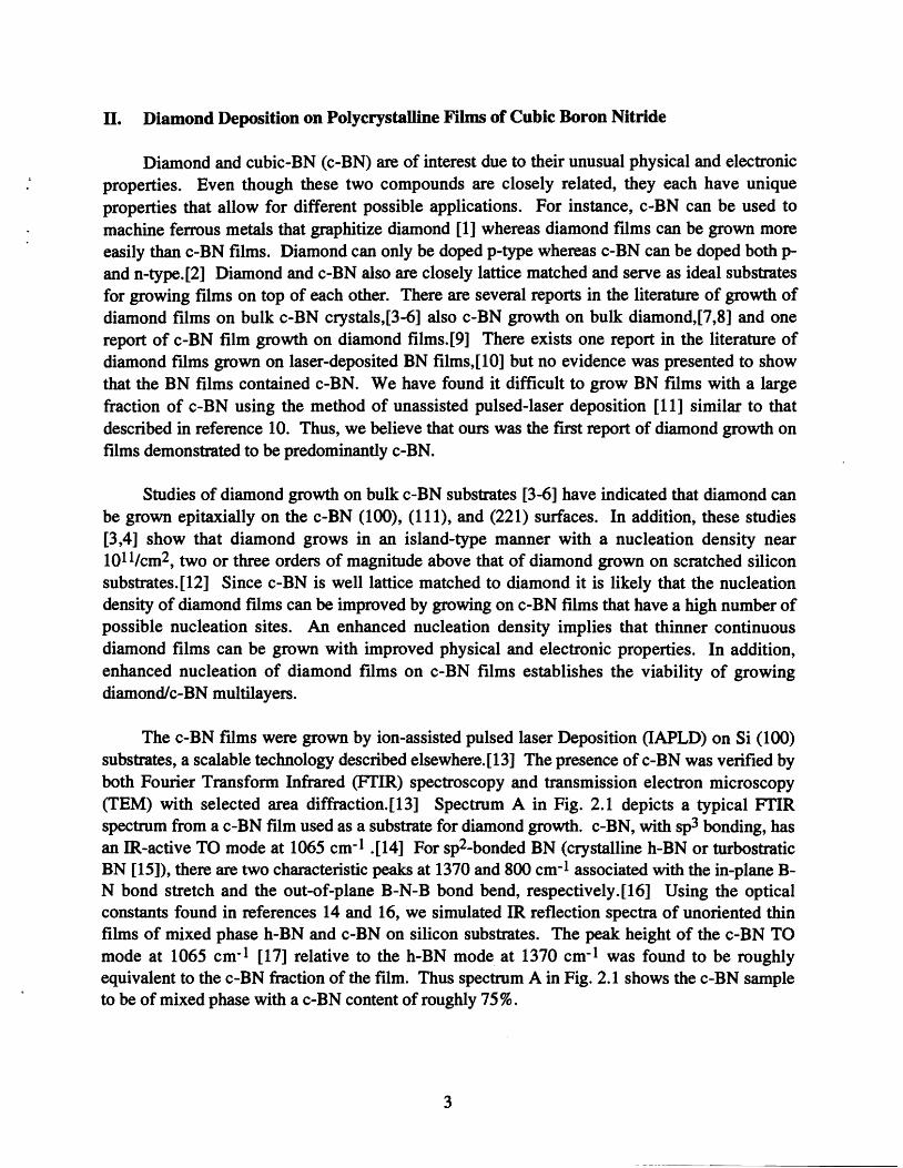
It was found that significant etching of the c-BN films occurred when exposed to the hot filament reactor conditions. c-BN fums having thickness ~ 1500 Awere completely removed before diamond films nucleated. In contrast, diamond nucleated readily on c-BN films ~ 1500 A). This result underscores the need to show that diamond is actually nucleating on the c-BN film. For the sample in Fig. 2.1 the deposition was halted at 110 minutes, leaving diamond that had not coalesced into a continuous film. The FfIR spectrum labeled B in Fig. 2.1 was taken through the diamond overlayer, clearly revealing the presence of the c-BN IR mode at 1080 cm- I . A sample with a continuous diamond coating was made by running the diamond reactor for a slightly longer time of 165 minutes. FTIR spectra recorded before and after deposition in Fig. 2.3 reveal the clear presence of the c-BN IR mode near 1080 cm-I . The c-BN concentration for both samples (Figs. 1 and 3) was unchanged after diamond deposition. The sample in Fig. 2.2 was in the diamond reactor for 3 days producing a thicker film; it proved impossible to detect the c-BN film underneath with FTIR due to large interference reflections associated with the thick diamond coating. A depth sputtering profile measured using AES on a similar sample grown in the same manner confirmed the presence of boron and nitrogen in the region between the silicon and diamond. Thus, we have conclusively shown by both FTIR and AES that the diamond is nucleating on the c-BN film.
5
160
150
140
c 1300 '.fj (,)
CD 120'+=CD
c::: '#. 110
100
90
80 hBN cBN
A. Befcre diamood deposition
hBN
B. After darrond deposition
500 1000 1500 2000
Wavenumber <1 I cm)
Fig. 2.3 FfIR spectra of a c-BN film taken a) before and b) after 165 minutes in the diamond reactor. The diamond overlayer was continuous, producing an interference reflection which varied sinusoidally with wavenumber in the IR spectrum. This background sine wave has been subtracted from the data shown in spectrum b. The c-BN IR mode at 1080 cm-1 is evident in both spectra.
SEMs of the non-continuous diamond sample (FTIR spectra shown in Fig. 1) were recorded to estimate the nucleation density of the diamond; one of these SEMs is shown in Fig. 2.4. The nucleation density of this diamond film was conservatively estimated to be 1 xl09
/cm2, at least as high as scratched SL[12] The estimation was made by counting diamond particles ~ 0.2 J,lm in size contained in a square region. Nucleation densities were measured at several different places on this film, and on several different samples, all giving similar results. The difference between the nucleation density of diamond on bulk c-BN (1 xl011/cm2) and our result on thin films is probably related to the polycrystalline and mixed phase nature of the c-BN films.[3,4] All of the exposed surfaces of the c-BN grains may not nucleate diamond as readily as the surfaces studied in those reports. In addition the films consist of roughly 25 % sp2-bonded h-BN that may also have a low nucleation density for diamond.
To directly compare the nucleation density of diamond on unscratched Si substrates versus that of c-BN films, a c-BN film was grown on a partially masked Si substrate, producing a c-BN film region and a bare Si region. This substrate was then inserted in the diamond reactor exposing both the bare Si and the c-BN-coated Si to the hot filament. The reactor was run for 110 minutes. Fig. 2.5 is an SEM photo taken of the interface region between the Si and the c-BN film. The diamond nucleation on the c-BN side is clear with almost a continuous coating of
6

diamond evident at a nucleation density estimated to be 1 x l09/cm2. In contrast, the bare Si shows a diamond nucleation density of - lOSlcm2.
Fig. 2.4 SEM photograph of diamond grown on a c-BN film. The FfIR spectra of this sample are shown in Fig. 1. The diamond nucleation density on the c-BN film is conselVatively estimated to be 1 xl09/cm2•
Fig. 2.5: SEM photograph of a diamond film grown on a substrate that was masked such that half was Si and the other half was a c-BN film on Si. The region shown is the interface between the Si (right side) and the c-BN film (left side). The diamond nucleation density on the c-BN film is estimated to be 1 xl09/cm2• In marked contrast, the Si shows a diamond nucleation density of -lOSlcm2.
Using a hot filament reactor, we grew diamond films on polycrysta1line c-BN fums that are produced by ion-assisted PLD. There was no surface pretreatment of the c-BN films prior to diamond deposition. We verified the presence of c-BN beneath the diamond by FfIR and used AES depth profiling to confmn the presence of boron and nitrogen between the Si and diamond. The nucleation density of the diamond on c-BN was estimated to be 1 x l09/cm2• This value is
7

at least as high or higher than the nucleation density of diamond on pretreated Si substrates. This work has shown that it is possible to increase markedly the nucleation density of diamond films by growing on c-BN films without mechanically abrading the deposition surface. This result enhances the possibility that thinner continuous diamond films can be grown which are suitable for use in multilayer structures and electronic devices.
References
1. L. Vel, G. Demazeau and J. Etourneau, Mater. Sci. and Eng. B 10, 149 (1991). 2. O. Mishima. in Synthesis and Properties of Boron Nitride (eds. J.J. Pouch & S.A.
Alterovitz) pp. 313-328 (Materials Science Forum 54.55, Trans Tech Publications LTD, Aedermannsdorf, 1990).
3. T. Inuzuka and S. Koizumi, SPIE Diamond Optics ill 1325, 2 (1990). 4. S. Koizumi, T. Murakami, T. Inuzuka and K. Suzuki, Appl. Phys. Lett. 57, 563 (1990). 5. M. Yoshikawa, H. Ishida, A. Ishitani, T. Murakami, S. Koizumi and T. Inuzuka, Appl.
Phys. Lett. 57,428 (1990). 6. M. Yoshikawa, H. Ishida, A. Ishitani, S. Koizumi and T. Inuzuka, Appl. Phys. Lett. 58,
1387 (1991). 7. H. Saitoh and W. A. Yarbrough, Appl. Phys. Lett. 58,2482 (1991). 8. H. Sei, M. Akaishi, H. Kanda, T. Osawa and S. Yamaoka, New Diamond Science and
Technology 1057 (1991). 9. M. Murakawa and S. Watanabe, Surface and Coatings Technology 43/44, 145 (1990). 10. S. M. Kanetkar, G. Matera, X. Chen, S. Pramanick, P. Tiwari, J. Narayan, G. Pfeiffer and
M. Paesler, Journal of Electronic Materials 20, 141 (1991). 11. T. A. Friedmann, K. F. McCarty, E. J. Klaus, J. C. Barbour, W. M. Clift, H. A. Johnsen, D.
L. Medlin, M. J. Mills and D. K. Ottesen, accepted in "Thin Solid Films" (1993). 12. K. Suzuki, A. Sawabe, H. Yasuda and T.lnuzuka, Appl. Phys. Lett. 50, 728 (1987). 13. T. A. Friedmann, W. M. Clift, H. A. Johnsen, E. J. Klaus, K. F. McCarty, D. L. Medlin, M.
J. Mills, and D. K. Ottesen, in Laser Ablation in Materials Processing: Fundamentals and Applications, D. Braren, J. J. Dubowski, and D. P. Norton, Eds. (Materials Research Society, Pittsburgh PA, 1993), vol. 285, pp. 507-512.
14. P. J. Gielisse, S. S. Mitra, J. N. Plendl, R. D. Griffis, L. C. Mansur, R. Marshall and E. A. Pascoe, Phys. Rev. 155, 1039 (1967).
15. J. Thomas, Jr., N. E. Weston and T. E. O'Connor, J. Amer. Chem. Soc. 84,4619 (1963). 16. R. Geick, C. H. Penny and G. Rupprecht, Phys. Rev. 146,543 (1966). 17. We find the c-BN mode at 1080 cm-1 shifted up from the bulk value of 1065 cm- 1,
possibly due to internal stress in the film. 18. E. Kondoh, T. Ohta, T. Mitomo and K. Ohtsuka, Appl. Phys. Lett. 59,488 (1991). 19. S. Matsumoto, Y. Sato, M. Kamo and N. Setaka, Jpn. J. Appl. Phys. 21, 1183 (1982). 20. B. Singh, Y. Arie, A. W. Levine and O. R. Mesker, Appl. Phys. Lett. 52,451 (1988). 21. L. Bernardez, K. F. McCarty and N. Yang, J. Appl. Phys. 72,2001 (1992).
8
---------------------
ID. Experimental Results from Attempted CVD Growth of Diamond on a-tC.
A series of experiments to test the feasibility of growing hot filament assisted CVD diamond films on thin films of a-tC were performed. It was thought that a-tC might provide a high density of nucleation sites leading to enhanced diamond nucleation or other unique diamond film properties. Nucleation of diamond films on a-tC has been elusive due to the high etch rate of a-tC in an atomic hydrogen rich atmosphere. Atomic hydrogen is believed to be necessary in the CVD growth of diamond films.
The etch rate for a-tC was - 150-250 Alminute. Annealing or even completely decomposing the a-tC to a form glassy carbon (amorphous graphite) does not slow the etch rate enough to allow the diamond to nucleate. Under our experimental conditions, the etch rate of atC is too high to allow diamond to be nucleated and grown. It may be possible, however, to use the ability of atomic hydrogen to etch a-tC to an advantage. Atomic hydrogen may be useful for selective etching in the processing of devices incorporating at-C.
IV. Growth and Characterization ofa-tC by Pulsed Laser Deposition in ffigh Vacuum
Diamond-like carbon (OLC) is an amorphous or nanocrystalline mixture of sp2 and sp3 carbon-carbon bonds. Due to its similar properties with diamond, DLC is often considered as an inexpensive alternative to diamond films for many applications. It is typically grown at lowtemperatures by a plasma chemical-vapor deposition (CVD) method using methane (CI4) gas as the carbon source. These materials incorporate large amounts of hydrogen into their structure (~ 20 atomic percent) with C-H bonds accounting for the high tetrahedral coordination of the carbon atoms. Such films can be denoted as a-C:H, indicating an amorphous carbon-hydrogen material. a-C:H films can be grown to have either their hardness or optical transparency optimized to act as a substitute for diamond [1]. Such films rarely have well-controlled electrical properties and are stable to temperatures only to 250 - 300·C, well-below that required for most microelectronic device processing. Above these temperatures, hydrogen evolves from the films and is accompanied by the conversion of C-C bonds from sp3 to sp2 hybridization, resulting in an overall film structure of micro-crystalline graphite, also known as "glassy" carbon [2]. Glassy carbon is closer to graphite in its properties rather than to diamond. The material is relatively soft and electrically conductive.
Several methods have been developed to deposit DLC films without intentionally adding hydrogen, including the filtered cathodic arc, ion-beam, and pulsed-laser deposition (PLD) [3 12]. This section studies the structural and electrical properties of fums grown by PLD in a highvacuum ambient. Note that this type of DLC is grown without significant hydrogen content, and has many of the properties associated with diamond films and is stable to temperatures higher than a-C:H [14]. To differentiate films grown in this manner, we denote them as highlytetrahedral-coordinated-amorphous-carbon (a-tC). a-tC films can be grown in a variety of ambient conditions, trapping impurity atoms into its structure. During deposition, background
9

gases composed of H2, N2 and Ar could be fed into the chamber and their pressure controlled by a throttle valve and measured with a capacitance based pressure transducer capable of reading absolute pressure. In this manner background pressures could be regulated from the base pressure of the chamber up to 1 Torr of gas pressure.
a-tC films are grown by PLD, shown in Figure 4.1, using 248 nm excimer pulsed-laser radiation (KrF), from a pyrolytic graphite target, onto rotating p-type (1019 B atomslcm-3) Si (100) substrates. Target-substrate distance is .... 5 inches. With the use of appropriate geometry, as described in reference 13, thickness uniformity within ±5% is achieved over 2-inch diameter wafers. The substrates are cleaned using a standard HFINH4F dip to remove the surface oxide before loading into the vacuum chamber (base pressure < 10-7 Torr) [15]. The substrates are not purposely heated during deposition, although some residual heating to T ~ 50·C may occur as a result of the deposition process. Laser pulses (duration .... 17 ns) are focused on to a rectangular spot off the center of the rotating target (to prevent excessive cratering) with an area of 0.01 cm2.
A repetition rate of 20 Hz is used. Energy density is varied from 5 - 45 J/cm2• Deposition rates .... 1 Als are achieved. Films ranging from 100 - 3500 A thick have been grown.
Mi rro r Exci mer laser
I
KrF 248 nm 0.4 J/pul se
Rotatabl e
Fig.4.1: A diagram of the chamber used to deposit the films.
Film thicknesses and residual stresses are determined using a stylus profilometer. Atomicforce microscopy (AFM) is used to determine film morphology. Raman spectroscopy (A. = 514 nm, power =50 mW) is used to differentiate the various forms of carbon [16]. Electrical characterization is performed by conventional current-voltage (I-V) and capacitance-voltage (CV) measurements. Gold, titanium, and mercury-metal contacts are used. Electrical and structural properties are measured as a function of laser-energy density used during film growth.
10

Characterization of the samples is accomplished mainly by Raman spectroscopy, which serves to differentiate between various forms of carbon. The films were measured with 514 nm light at 50 m W of power. Fig. 4.2 depicts five Raman spectra of different forms of carbon ranging from graphite to diamond. For graphite there are two active modes at 1350 cm- l and 1581 cm- l . The Raman band at 1580 - 1590 cm- l is a fundamental Brillouin-zone-center mode of graphite. The Raman band at 1350 - 1360 cm- l is believed to be a Brillouin-zone-edge phonon mode that intensifies for graphite crystal domains less than 100 nm in size. Glassy carbon is a disordered graphitic phase with broad Raman peaks near 1360 cm- l and 1590 cm- l .
Diamond has one active Raman mode at 1332 cm- l characteristic of sp3-bonded carbon. Conventional a-C:H has a broad asymmetric Raman peak near 1515 cm- l with a long tail that extends down to -1000 cm- l . at-C also has a single broad Raman mode, but this mode is shifted up to higher wavenumber (1565 cm- l ) and is more symmetric than that of a-C:H. This peak arises from sp2-bonded carbon atoms. The presence of sp3-bonded carbon is not obvious in these spectra due to the resonance enhancement of the sp2-bonded atoms at the laser wavelength used. Thus, the signal from sp2-bonded carbon atoms tends to obscure any signal due to sp3bonded carbon atoms making it difficult to determine the actual sp3 content of the film from Raman measurements.
".... III ...., ·s :l )'\ ' as ' ...., :s -< '
....... III...., C ::J 0 u
800
1332 I.t)
CD I.t) Dianald
at-C
a-C:H
1350 Graphite
1000 1200 1400 1800 2000 Wavenumber (cm)-l
Fig. 4.2: Representative Raman spectra for five forms of carbon. Note the difference in peak position and shape between the at-C and a-C:H spectra.
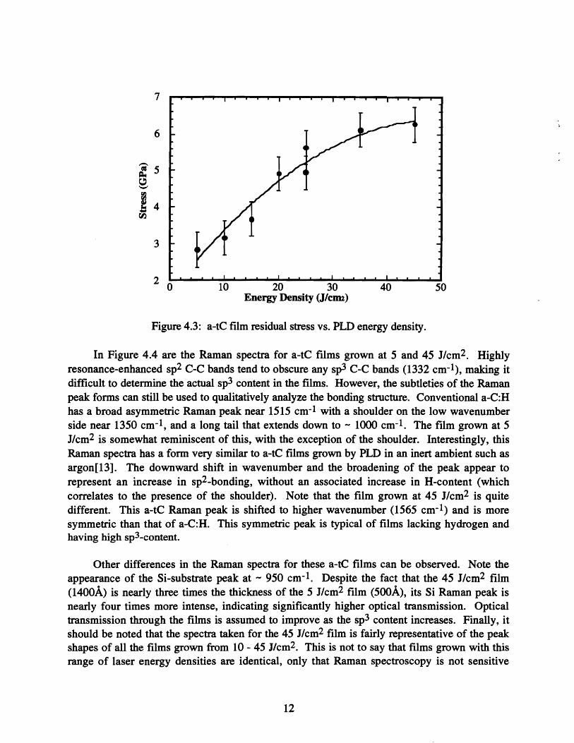
a-tC films grown on the Si-substrates have mirror-like surfaces, and AFM detects no structure on a nonsocial. Film stress is determined using a profilometer, by measuring actual wafer curvatures before and after a-tC film deposition. Figure 4.3 shows the stresses resulting from films grown with laser energy densities ranging from 5 to 45 J/cm2. Note that these stresses are greater than 6 GPa for the highest energy densities used for film growth. This large stress for the 45 J/cm2 films limits their thickness to - 3500A before delamination occurs. As the laser pulse energy is reduced, thicker films can be grown without delaminating due to the decrease in the residual film stress.
11
7
6
3
2 0 10 20 30 40 50 Energy Density (J/elD2)
Figure 4.3: a-tC film residual stress vs. PLD energy density.
In Figure 4.4 are the Raman spectra for a-tC films grown at 5 and 45 J/cm2. Highly resonance-enhanced sp2 C-C bands tend to obscure any sp3 C-C bands (1332 cm- I ), making it difficult to determine the actual sp3 content in the films. However, the subtleties of the Raman peak forms can still be used to qualitatively analyze the bonding structure. Conventional a-C:H has a broad asymmetric Raman peak near 1515 cm- I with a shoulder on the low wavenumber side near 1350 cm- I , and a long tail that extends down to - 1000 cm- I . The film grown at 5 J/cm2 is somewhat reminiscent of this, with the exception of the shoulder. Interestingly, this Raman spectra has a form very similar to a-tC films grown by PLD in an inert ambient such as argon[13]. The downward shift in wavenumber and the broadening of the peak appear to represent an increase in sp2-bonding, without an associated increase in H-content (which correlates to the presence of the shoulder). Note that the film grown at 45 J/cm2 is quite different. This a-tC Raman peak is shifted to higher wavenumber (1565 cm- I ) and is more symmetric than that of a-C:H. This symmetric peak is typical of films lacking hydrogen and having high sp3-content.
Other differences in the Raman spectra for these a-tC films can be observed. Note the appearance of the Si-substrate peak at - 950 cm- I . Despite the fact that the 45 J/cm2 film (1400A) is nearly three times the thickness of the 5 J/cm2 film (500A), its Si Raman peak is nearly four times more intense, indicating significantly higher optical transmission. Optical transmission through the films is assumed to improve as the sp3 content increases. Finally, it should be noted that the spectra taken for the 45 J/cm2 film is fairly representative of the peak shapes of all the films grown from 10 - 45 J/cm2. This is not to say that films grown with this range of laser energy densities are identical, only that Raman spectroscopy is not sensitive
12

enough to distinguish any major differences. A more detailed study of these films and correlations to the electronic structure is underway.
800 1000 1200 1400 1600 1800 2000 Wavenumber (em)-!
Figure 4.4: Raman spectra for a-tC films grown at 5 and 45 J/cm2•
The thermal stability of the highest sp3-content a-tC films is determined by performing annealing studies using in-situ Raman spectroscopy. Samples are heated in flowing argon and Raman spectra taken at progressively higher temperatures. The upper spectrum in Figure 4.5 shows the film at exposure to 700·C after 10 minutes. Importantly, the Raman peak-shape is essentially unchanged from the room-temperature spectrum (not shown). Since blackbody background above 700·C swamps the Raman signal, spectra are taken at 700·C after cooling from higher temperatures. Even after heating to l000·C for 10 minutes (lower spectrum), there was no apparent change in the a-tC film. This robust stability of PLD-produced a-tC is in marked contrast to aC:H, the commonly studied material. Recall that the latter material desorbs H and graphitizes at temperatures above -300·C [2].
The electronic properties of a-tC films have been evaluated. Schottky barrier behavior is observed at the a-tC/metal interface for Hg, Au, or Ti metal contacts. Current-voltage and capacitance-voltage measurements, taken at room-temperature, are shown in Figures 4.6 and 4.7, respectively, for a 1000A-thick a-tC film grown on Si (p-type, 1019 cm-3) with a mercury contact. As shown in Fig. 4.6, non-ideal diode behavior is observed, with the polarity indicating that the a-tC is a p-type semiconductor. Consistent with this picture of carrier type, the C-V data display depletion of the a-tC under reverse bias. The p-type doping of the a-tC is approximately mid-l016 cm-3. At large reverse bias, the capacitance becomes approximately constant, corresponding to the geometric capacitance of the a-tC film. The geometric capacitance varies with the inverse of the a-tC film thickness, resulting in a a-tC dielectric permittivity constant of E
13

=4. As shown in Fig. 4.7, the capacitance displays a strong frequency dependence, increasing at lower frequency. This is a characteristic of a distribution of charge trap states in energy within the a-tC film.
a-tC at 700·C after exposure
to l000·C in Ar
1600 1800 20001000 1200 1400 Wavenumber (cm)-l
Fig. 4.5: In-situ Raman spectra of an a-tC film taken at elevated temperatures in flowing Ar.
T=300K Forward bias
o 0.5 1 1.5 2 2.5 3 Bias Voltage (V)
Figure 4.6: I -V characteristic of a Si (p-type )/a-tC (I000A)lHg structure.
14

10
(6x10¹⁶ acceptors/cm3)
o 1 2 3 Reverse-bias voltage (V)
Figure 4.7: C-V data on the same structure for different modulation frequencies.
In summary, highly tetrahedral-coordinated-amorphous-carbon (a-tC) films can be grown by pulsed-laser deposition onto silicon substrates maintained essentially at room-temperature. Remarkably, these same films remain thermally stable to temperatures at least as high as l000·C. These a-tC films have optically-smooth surfaces, with no detectable structure using atomic-force microscopy. Laser energy density is directly related to both a-tC residual film stress and Raman structure, i.e., to the sp2 - sp3 carbon-carbon bond ratio. Film stress can be relieved without grossly affecting the Raman spectra, however, effects on electronic properties have yet to be determined. a-tC films grown with the highest sp3-content are semiconducting (p-type, - mid1016 acceptors/cm3). The permittivity dielectric constant has been determined to be £ - 4, essentially the same as that of diamond.
References
1. S. Kaplan, F. Jansen, and M. Machonkin, Appl. Phys. Lett. 47, 750 (1985).
2. J. E. Parmeter, D. R. Tallant, and M. P. Siegal, presented at the 1994 MRS Spring Meeting, San Francisco, CA 1994 (published in these proceedings).
3. S. D. Berger, D. R. McKenzie, and P. J. Martin, Philos. Mag. Lett. 57, 285 (1988).
4. R. Lossy, D. L. Pappas, R. A. Roy, and J. J. Cuomo, Appl. Phys. Lett. 61, 171 (1992).
5. J. J. Cuomo, J. P. Doyle, J. Bruley, and J. C. Liu, J. Vac. Sci. Technol. A 9, 2210 (1991).
6. C. Weissmantel, C. Shurer, F. Frohlich, P. Grau, and H. Lehmann, Thin Solid Films 61, L5 (1979).
7. F. Xiong, Y. Y. Wang, V. Leppert, and R. P. H. Chang, J. Mater. Res. 8, 2265 (1993).
15

8. C. B. Collins, F. Davanloo, D. R. Jander, T. J. Lee, H. Park, and J. H. You, J. Appl. Phys. 69, 7862 (1991).
9. F. Davanloo, E. M. Juengennan, D. R. Jander, T. J. Lee, and C. B. Collins, J. Appl. Phys. 67, 2081 (1990).
10. J. Krishnaswamy, A. Rengan, J. Narayan, K. Vedam, and C. J. Mcharque, Appl. Phys. Lett. 54, 2455 (1989).
11. C. L. Marquardt, R. T. Williams, and D. J. Nagel, in Plasma Synthesis and Etching of Electronic Materials, R. P. H. Chang, and B. Abeles, Eds. (Materials Research Society, Pittsburgh, 1985), vol. 38, p. 325.
12. D. L. Pappas, K. L. Sanger, J. Bruley, W. Krakow, J. J. Cuomo, T. Gu, and R. W. Collins, J. Appl. Phys. 71,5675 (1992).
13. T. A. Friedmann, M. P. Siegal, D. R Tallant, R. L. Simpson, and F. Dominguez, presented at the 1994 MRS Spring Meeting, San Francisco, CA 1994 (published in these proceedings).
14. F. Xiong, Y. Y. Wang, and R. P. H. Chang, Phys. Rev. B 48, 8016 (1993).
15. G. S. Higashi, Y. J. Chabal, G. W. Trucks, and K. Raghavachari, Appl. Phys. Lett. 56, 656 (1990).
16. D. R. Tallant, J. E. Parmeter, M. P. Siegal, and R. L. Simpson, Diamond and Related Materials (to be published).
16

V. a-tC Thin Films Grown by PLD in Various Gas Ambients
The wafer curvatures before and after deposition as well as the sample thicknesses were measured using a stylus profilometer. The residual stresses in the films, uI ' could then be calculated using [1,2]:
(1)
where Es is Young's modulus for the substrate, v is Poisson's ratio for the substrate [20], ts is the substrate thickness, tI is the film thickness, and R is the radius of curvature. The maximum error in the stress measurements was estimated to be -15% due to errors in measuring the film thickness and radius of curvature. For the films grown in this study the residual stress was always compressive.
Fig. 5.1 depicts the residual stress versus pressure for samples grown in an Ar ambient gas. The film grown in vacuum shows a residual stress level near 8 GPa. This high level of stress limits the maximum film thickness (-3000 A) due to stress induced spalling of the film. The residual stress decreases linearly with increasing Ar pressure. At these lower stress levels the films can be grown thicker (>3000 A) before spalling from the substrate. The reduction in residual stress with pressure is probably due to collisional cooling of the ablated plume by the ambient background gas. The average energy distribution of carbon species in the plume would be reduced and broadened. This would reduce the stress in the growing film by reducing the number of vacancies and interstitials produced upon impact, and consequently reducing the sp3 content of the films. However, it must be noted that the deposition rate also decreases with increasing gas pressure (from -1.0 Als to -0.2 Als over the pressure range studied) so that films grown at higher pressures are thinner and experience a lower fluence than those grown in vacuum. The lower fluence at higher pressures may also contribute to the stress reduction, since the dynamics of the stress formation process (creation and annihilation of vacancies and interstitials) will also be changed.
Fig. 5.2 depicts a plot of the residual stress versus pressure for samples deposited in hydrogen and nitrogen ambients. For hydrogen, a linear relationship between the stress and pressure is observed, very similar to the films grown in an Ar ambient gas. For nitrogen, there appears to be a break in the stress versus pressure curve near 20 mTorr of gas pressure; and the residual stress level falls faster than for H2 or Ar. If the stress level correlates to the percentage of sp3-bonded carbon atoms, then it appears that nitrogen is more effective in reducing the sp3 content of the films. However, as will be shown below, both hydrogen and nitrogen are chemically incotpOrated into the films at these pressures. In the case of hydrogen incorporation, it is likely that C-H bonds maintain the high fraction of tetrahedrally coordinated carbon atoms (similar to a-C:H). For the case of nitrogen incotpOration, sp2-bonded configurations are more likely, leading to a faster reduction in residual stress with pressure.
17
10 ...........- ................-...--......- ........... - .......
8 CD Ngoo
o 10 20 30 40 50o ----------------~----------Pressure (mTor r)
Fig. 5.1: Residual compressive stress vs. pressure for samples grown in an Ar ambient gas.
8
7
6
.-.5ra Q.
~4 en en 3 ~ ..,Cl)2
1
CD HycrOgEn
lSI Ni tro gen
lSI
o ~----~----~--------~------~o 10 20 30 40 50 Pressure (mTorr)
Fig. 5.2: Residual compressive stress vs. pressure for H2 and N2 background gases. Note the break in slope for the nitrogen data near 20 mTorr. The lines are drawn as guides to the eye.
To examine the nature of the bonding, Raman spectra were obtained from these films and are depicted in Fig. 5.3. Fig. 5.3a shows three representative Raman spectra from samples grown in an Ar ambient. The relatively sharp Raman band at -950 cm-1 is due to the silicon substrate. As the Ar gas pressure increases, the silicon Raman band decreases in intensity indicating that the samples become less transparent. (Since the samples decrease in thickness at higher gas pressures, this effect is even greater than depicted in Fig. 5.3a.) This is consistent with the lower stress level observed at high gas pressure and is possibly due to increased absorption from graphitic elements in the film.
18

As the gas pressure increases, the at-C Raman peak shifts from a relatively symmetric band near 1565 cm-I to a broadened asymmetric band peaked near 1520 cm- I . This change in peak shape and position reflects some change in bonding configuration and/or distribution for the sp2bonded carbon in the film. We speculate that collisional cooling may broaden the energy distribution of the ablated carbon species leading to a wider distribution of sp2-bonded ring structures in the film.
Fig. 5.3b depicts representative Raman spectra taken from films deposited in a hydrogen background gas. The Raman spectra evolve smoothly with increasing H2 pressure. This correlates well with the linear change in the stress with H2 pressure. As is the case with the films deposited in Ar the intensity of the Si Raman band decreases (this is not apparent from Fig. 5b due to the increased scale of the graph) with increasing gas pressure indicating that the films are more absorptive. The at-C peak shifts down in wavenumber (from 1565 cm-I to 1520 cm-I ) and also becomes dramatically more intense indicating that the Raman scattering efficiency is increasing. (The sample deposited in vacuum is plotted with the same intensity in Figs. 5.3a, 5.3b, and 5.3c.) In addition, there is a distinct shoulder that develops near 1300 cm- I . This shoulder does not appear for the samples deposited in Ar, and could be a result of hydrogen incorporation into the film, for it resembles the Raman spectra of a-C:H shown in Fig. 2.
Fig. 5.3c depicts representative Raman spectra taken from films deposited in a nitrogen background gas. The silicon Raman band also decreases with increasing gas pressure indicating that the samples are more absorptive. The Raman spectra show a sharp increase in intensity above 20 mTorr of gas pressure, which correlates with the break in residual stress with pressure noted above. In addition, the peak position of the at-C Raman band shifts downward as the intensity of the band increases dramatically. A well developed shoulder also appears near 1380 cm- I . This band is most likely due to nitrogen incorporation into the film and represents C-N bonding.
In general, we note that the Raman spectra show effects common to the presence of Ar, H2, and N2. These effects are increases in the Raman scattering efficiency, increases in absorption, and decreases in the at-C peak position. To varying degree, these effects may be generically related to the increased gas pressure with a concomitant slowing of the laser-ablated carbon species and attenuation of their fluence. Changes of the at-C line shape in N2 and H2 are most probably related to the chemical incorporation of these gases into the films, since these effects are dramatically different in the case of Ar.
Depositions were also undertaken in vacuum at varying laser energy densities [3]. At lower energy densities, the ejected carbon species should have a lower energy distribution, similar to the effect of adding a non reactive background gas. The resultant Raman spectra from these films are very similar to those grown in an Ar ambient gas.
We find that changes in the residual stress of films grown by pulsed laser deposition can be correlated with changes in the Raman spectra. In general, as the pressure of the background gas
19
-~ C :::t
of! '"-en 1: :::t
30 20
VaaJum
Hz pressure (mTar)
50 25 20 11 5
VaaJum
50 25 20
VaaJum
a)
c)
8L-~~~~~~~~~
increases the residual compressive stress in the films decreases. The Raman spectra show an increase in the Raman scattering efficiency, an increase in opacity, and a decrease in the peak position and symmetry of the at-C Raman band. These effects may all be related to collisional cooling of the ablated carbon species by the background gas. In the case of Ar and H2 ambients the change in stress with pressure was linear, and the resultant Raman spectra revealed a smooth evolution with pressure. In the case of a N2 ambient, the stress changed abruptly with pressure near 20 mTorr; and the resultant Raman spectra showed a sharp increase in intensity and the development of a band at 1380 cm-1 associated with the incorporation of nitrogen into the film.
Ar pressure (mTorr)
Wavenumber (em)-1
Fig. 5.3: Raman spectra for samples grown in a) Ar, b) H2, and c) N2 background ambients. Note that the spectrum for the sample grown in vacuum is plotted with the same intensity on each graph.
20

References
1. N. N. Davidenkov, Sov. Phys. Sol. State 2,2595 (1961). 2. R. W. Hoffman, Phys. Thin Films 3, 211 (1966). 3. M. J. Siegal, T. A. Friedmann, S. R. Kurtz, D. R. Tallant, R. L. Simpson, F. Dominguez,
and K. F. McCarty, in Novel Forms o/Carbon II, C. L. Renschler, D. Cox, J. Pouch, and Y. Achiba, Eds. (Materials Research Society, Pittsburgh, 1994).
21

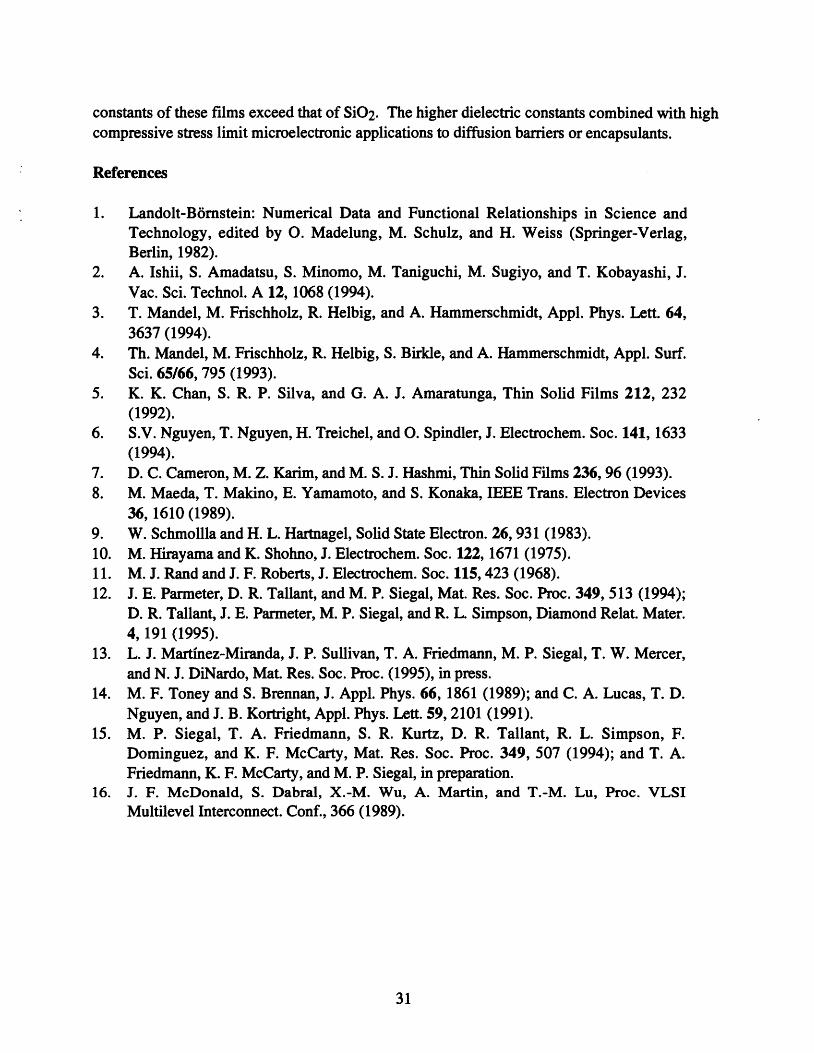
VI. Thermal Stability of a-tC Films Grown by PLD
This section discusses the thermal stability in vacuum of a-tC films grown by pulsed laser deposition (PLD). a-tC films with a high percentage of sp3 bonds are grown by PLD using an ultra-violet excimer laser. The details of the deposition process have been described previously. Films grown in this study were deposited on room temperature p-Si (100) substrates by ablating pyrolytic graphite targets with 248-nm light at a 20 Hz repetition rate to thicknesses of -2000A. The films were grown at varying laser fluence (12, 22, and 45 J/cm2) in vacuum, and at high laser fluence (45 J/cm2) in a background gas of either hydrogen or nitrogen.
The thermal stability of these films was assessed by annealing the samples in vacuum and recording changes to the films using in situ Raman spectroscopy (514-nm laser light). After film growth, the samples were cut into rectangular pieces, and Raman spectra were recorded from each sample at 20·C. Next, thermocouples were cemented to the backside of the specimens using a ceramic paste, followed by a 100 ·C anneal in air to set the paste. The samples were then mounted in a vacuum chamber, pumped to 10-7 Torr vacuum and resistively heated for various temperatures and times.
Initially, a set of samples was annealed at 5OO·C in vacuum for 15 hr. The specimens were cooled in vacuum to room temperature and Raman spectra were measured again. The Raman spectra before and after annealing for selected samples are shown in Fig. 6.1. Before annealing, the spectra from the samples grown in vacuum at different fluences are similar. They show a relatively symmetric peak near 1587 cm- I that is associated with sp2-bonded carbon atoms, typical of a-tC films [1, 2]. No peak for sp3-bonded carbon atoms can be seen in part due to resonant enhancement of the signal from sp2 bonds (-50x) at the laser wavelength used. In comparison, the peak positions in the spectra for the unannealed samples grown in background gases of nitrogen and hydrogen are shifted down in frequency (-1560 cm- I ); the Raman peak of the sample grown in nitrogen also shows an asymmetric tail extending to a lower Raman shift. These changes are probably a result of both collisional cooling of the ablation plume with the background gases leading to a higher sp2-bonded carbon fraction, and due to nitrogen and hydrogen incorporation in the films [1, 3]. Rutherford back scattering spectroscopy on samples grown in nitrogen under similar conditions shows the nitrogen to carbon composition ratio N/C = 0.10.
After annealing to 500·C, there is a progressive change in the Raman spectra with decreasing fluence. For the vacuum-grown films, the main Raman peak narrows slightly and develops a low Raman-shift tail for the lowest fluence (12 J/cm2) film. The samples grown in nitrogen and hydrogen background gases show more dramatic changes with annealing. The main Raman peak of the sample grown in nitrogen narrows and a well defined second peak appears near 1385 cm-I . The main Raman peak of the sample grown in hydrogen narrows even further and a long tail develops that extends out to lower Raman shift.
22
Background gas pressure
22
12
45
1000 1200 1400 1600 1800 2000 Wavenumber (cm-')
Fig. 6.1 Room temperature Raman spectra for as deposited and annealed samples (500·C in vacuum).
A more thorough study was performed on selected samples to map the evolution of the Raman spectra with temperature. In this study, the samples were heated higher temperatures in the following manner. Thermocouples were initially attached to the samples as described above, and a baseline spectrum was acquired at 20·C. The samples were then annealed (in vacuum) at elevated temperature for 30 minutes and cooled to 200·C, at which temperature a Raman spectrum was measured. This procedure was repeated (without breaking vacuum) by heating to progressively higher temperatures and acquiring spectra at 200·C.
The data for samples grown at high fluence (45 J/cm2) in vacuum and in a background gas of nitrogen are shown in Figs. 6.2a and 6.2b, respectively. For the sample grown in vacuum (Fig. 6.2a), there is little evidence of change in the main Raman peak until the annealing temperature reaches - 8OO·C. Above this point the Raman spectra gradually begin to resemble that of nanocrystalline graphite. For the sample grown in a nitrogen ambient (Fig. 6.2b), the Raman spectra are much more temperature sensitive. Even the spectrum taken at 20·C (after curing the thermocouple cement in air at I(XYC) shows considerable change in comparison to the unheated material (Fig. 6.1). The peak near 1385 cm-1 has grown in intensity and broadened.
23

----
en...·2 ::s .c... ~ til... C::s o o
.-.
.!·2 ::s .c... as
.! c::s o o
800 1000 1200 1400 1600
Raman Shift (cmr1
Fig.6.2 a.) Raman spectra acquired at 200 °C after annealing in vacuum to successively higher temperatures. The sample was grown at high laser energy density (45 J/cm2) in vacuum. b.) Raman spectra acquired at 200 °C after annealing in vacuum to successively higher temperatures. The sample was grown at high laser energy density (45 J/cm2) in vacuum.
24
Also evident in Fig. 6.2a is a peak at - 965 cm- l that is the second-order phonon scattering from the silicon substrate. The appearance of this peak is an indication of the transparency of the fIlm near the laser wavelength of 514 nm. The intensity of this peak as a function of annealing temperature for several samples is plotted in Fig. 6.3. For the fIlms grown in vacuum, the intensity of this peak decreases relatively smoothly with temperature, even at temperatures where little or no change in the a-tC Raman peak is detected. For the fIlm grown in a nitrogen background gas, the second-order Raman scattering from silicon is not evident even at the lowest temperatures indicating that the sample is more opaque than those grown in vacuum.
The transparency of these fIlms is a result of the high fraction of carbon atoms with tetrahedral coordination. Theoretical structural models of this material predict that there is a signifIcant amount of strain involved in the a-tC network [4]. It is not unreasonable that highly strained sp3 bonds are slowly converted to sp2 bonds with temperature. Since the sp3 bonds are not directly measured by Raman spectroscopy, this would result in higher absorption with little change in the a-tC Raman active peak. It is also possible that impurities in the vacuum (e.g., oxygen and hydrogen) are reacting with the heated fIlm.
The Raman spectra were fIt to two gaussian peaks in order to extract information regarding changes in the fIlm structure with annealing. For consistency with the published literature, we defIne these two peaks as the disorder ("D") and graphite ("G") peaks. (This notation arises from the Raman spectra of nanocrystalline graphite, which generally shows two peaks. One peak (-1590 cm-1) is due to the in-plane Raman mode of graphite, and the other (-1360 cm- l ) is attributed to small domain-size graphitic regions [5]. We note that the microstructure (amorphous) and bonding (a high fraction of sp3-bonded carbon atoms) of the unannealed specimens is quite different from nanocrystalline graphite and that this notation may be somewhat misleading. Fig. 6.5 is a plot of the integrated intensity ratio of the D to the G peak (10/10) determined from the fIts as a function of annealing temperature for selected samples. For the samples grown in vacuum, the ratio 10/10 is relatively constant till the annealing temperature reaches 800·C. At this point, the ratio begins to rise, which is consistent with a conversion of the a-tC structure into nanocrystalline graphite. For the sample grown in nitrogen, the 10/10 ratio increases until -400·C, plateaus between 400 and 800·C, and then increases again above 800·C. Possibly, nitrogen may evolve from the film at low temperature, thus converting parts of the fIlm to nanocrystalline graphite. By 400·C all the nitrogen has left the fIlm and the disorder peak does not grow in intensity. At 800·C the remaining portions of the fIlm with the a-tC structure begin to convert to nanocrystalline graphite.
In summary, we have explored the temperature stability of a-tC fIlms by in situ Raman spectroscopy of vacuum annealed fIlms. We fmd the thermal stability of fIlms is greatly affected by the addition of a background gas during growth. Films grown at high laser fluence in hydrogen and nitrogen background ambients show poor thermal stability with annealing. In contrast, a-tC fIlms grown in vacuum at high fluences are relatively stable up to 800·C, although changes in the opacity of the fIlms are occurring near room temperature.
25

References
1. T. A. Friedmann, M. P. Siegal, D. R. Tallant, R. L. Simpson, and F. Dominguez, in Novel Forms ofCarbon II, edited by C. L. Renschler, D. Cox, J. Pouch, and Y. Achiba (Materials Research Society, Pittsburgh, 1994), Vol. 349,.
2. F. Xiong, Y. Y..Wang, and R. P. H. Chang, Phys. Rev. B 48, 8016 (1993). 3. D. Thebert-Peeler, P. T. Murray, L. Petry, and T. W. Haas, in Phase Formation and
Modification by Beam-Solid Interactions, edited by G. S. Was, L. E. Rehn, and D. M. Follstaedt (MRS, Pittsburgh, 1992), Vol. 235, p. 879.
4. D. R. McKenzie, D. Muller, and B. A. Pailthorpe, Phys. Rev. Lett. 67, 773 (1991). 5. F. Tuinstra and J. L. Koenig, J. Chem. Phys. 53, 1126 (1969).
26

Vll. Evaluation of a-tC and BN Films as Low Permittivity Dielectrics
Insulators formed from first-row elements are good candidates for low permittivity dielectrics, with their bulk dielectric constants in the range - 5 to 8 for such materials as BeO, cBN, and diamond.[1] Insulating films of carbon are especially promising due to their compatibility with Si processing. Most studies have concentrated on chemical vapor or plasmaenhanced chemical vapor deposition (CVD and PECVD) which leads to insulating DLC films (films of amorphous carbon containing hydrogen). There have been numerous reports of the dielectric constants of these materials being less than or approaching that of Si02 (see Table 1).[2-11]
Film Dielectric Constant
Deposition Ref.
DLC 3.9 PECVD 2 DLC 4.2 PECVD 3 DLC 4.5 PECVD 4 DLC <4 PECVD 5
Table I: Reported dielectric constants for DLC films
Despite the low dielectric constants, these fIlms are not suitable as interlevel dielectrics due to thermal or environmental degradation. At temperatures above - 300°C, hydrogen comes out of DLC resulting in the transformation of C-C:H sp3 bonds to C-C sp2 bonds, as evidenced by changes in the Raman spectra and increased optical absorption.[12] This leads to non-insulating films which are unsuitable as an interlevel dielectric. The dielectric characteristics of these films are discussed below.
The a-tC films were deposited using PLD in high vacuum (10-8 - 10-7 Torr) with a KrF laser and a rotating graphite target. For some depositions, a background gas ofH2 or N2 (10 mTorr) was also used. The energy density of the laser light focused onto the rotating graphite target was adjusted between 5 to 48 J/cm2 leading to films with a varying degree of sp3 bonding. In all cases, deposition was performed at room temperature with no subsequent annealing.
For dielectric characterization, the a-tC films were deposited on heavily-doped (- 0.01 Ocm) n- and p-type Si substrates as well as on substrates containing a layer of TiW or TiN (- 2000 A) atop a thick layer of Si02 (- 1 JlID) on Si. Square and circular Ti-Au or AI contacts were made to the dielectric films either by photolithography and lift-off or by metal evaporation through a shadow mask. Diode sizes defined lithographically ranged from 50 Jlm to 400 Jlm, while those defmed by shadow mask ranged from - 127 Jlm to 1270 Jlm. Actual diode sizes were verified by optical microscopy. Backside contacts were made to the p-type wafers by an In-Ga eutectic alloy and to the n-type wafers by heat-diffused Sb, followed by the In-Ga eutectic. Typical film thicknesses for the a-tC films were 1000 A. Film thicknesses were measured by profilometry
27

and, on select samples, were corroborated by ellipsometry, transmission electron microscopy, or x-ray reflectivity. Uncertainties in the measured film thicknesses are estimated to be up to 10%, leading to uncertainties in the measured dielectric constants of up to 10%.
Current-voltage (IV) and capacitance-voltage (CV) characterization were performed on the metal-insulator-metal (MIM) and metal-insulator-semiconductor (MIS) diodes at frequencies ranging from 20 kHz to 4 MHz. The IV and CV measurements were performed for a variety of diode sizes to verify geometric scaling. Capacitances and AC conductances for the MIM diodes were typically found to vary by less than 5 % over the frequency range 20 kHz to 4 MHz, indicating negligible influence of any short time constant trap states in the bulk of the dielectric. The insulator capacitance was determined from the MIS diodes by biasing the device towards accumulation. Typically, a test frequency of 1 MHz was employed to reduce the contribution of any fast interface states.
The resistivities of a-tC films measured from MIM structures exhibit a strong dependence on the laser energy density and the presence or nature of the gas ambient in the deposition system. Resistivities (measured normal to the film plane) ranged from - 100 ncm for films deposited in vacuum at 5 J/cm2 to - 108 ncm for films deposited in vacuum at 48 J/cm2• Films deposited at 45 J/cm2 in 10 mTorr ambients of H2 or N2 showed resistivities> 106 ncm and less than 100 ncm, respectively. Sheet resistance measurements performed on a-tC films deposited on thick Si02 layers indicated resistivities > 106 ncm even for samples exhibiting resistivities normal to the film plane < 1()3 ncm, thus suggesting the existence of "shorts" - possibly graphitic - in the film. The requirements of an interconnect dielectric precludes the use of any but the most insulating a-tC films; therefore, dielectric characterization was performed only on the most insulating a-tC films.
The measured dielectric constants of a-tC fums, determined from MIM structures with TiW, as a function of laser energy density are shown in Fig. 7.1. The characteristics of a sample grown in 10 mTorr H2 is also shown. In all cases the normal film resistivities exceeded 106
ncm, and the phase angle of the measured admittance was close to -900 The solid circles •
indicate the mean of several measurements on one or two different samples at each deposition condition. The error bars reflect the total variation in measured dielectric constants for a particular sample deposition condition, not the error associated with each measurement of the dielectric constant (which is on the order of 10%, due to thickness uncertainty, as discussed above). For samples deposited in vacuum, the dielectric constant is essentially independent of laser energy density and falls within the range of 5 to 8, typically being close to 6.5. Sutprisingly, the sample deposited in an ambient of H2 exhibits a dielectric constant exceeding 8. It might be expected that a-tC films deposited in H2 ambients - which show Raman features similar to that of DLC - would show dielectric constants similar to that of DLC (about 4.0, see Table I). In contrast to the role of hydrogen in (PE)CVD deposition of DLC, a H2 gas ambient used with the PLD of carbon produces two effects: it results in the attenuation of the energies of the carbon species in the laser ablation plume, leading to the production of material with higher sp2 content - similar to the a-tC material deposited at lower laser energy densities; and, secondly,
28

hydrogen bonds to the trigonally-coordinated carbon, stabilizing the bonding into the sp3 coordination. Apparently the degree of hydrogen saturation of sp2 bonds in the a-tC material may not be as complete as that of DLC material (which is grown from a hydrogen containing precursor) and conductive regions of sp2 material may be present in the sample, thus contributing to higher apparent dielectric constants.
10 10 N/(N
2 + Ar) I = 2S0 J.lAIcm2
b
8 ____ 0.0 V =200V -.-0.1
b - 6II o.s •6a.CJ g-• Q•!4 •4a. tiS Q
2 ~
° 0
° 100 200 300 400 500 SOO 700 Current Density (J =It/A)
Fig. 7.1: Measured dielectric constants for a-tC films deposited in vacuum and hydrogen as a function of laser energy density.
Because of the potential for carbon reaction with the TiW bottom electrode of the MIM structures and uncertainties this may introduce, the dielectric constant for a-tC films using MIM structures with TiN and MIS structures with heavily-doped n- and p-type Si were also evaluated. Simultaneous depositions on the four types of substrates were performed at the highest laser energy density, 45 J/cm2, to ensure the creation of the most insulating material. A histogram of the measured dielectric constants is shown in Fig. 7.2. The measured dielectric constant peaks at about 6.5, independent of the substrate or MIMlMIS structure.
15
rJ a-tCITiW
• a-tCITiN
10 0 a-tCln+ -Si &.
~! a-tC/p+ -Si § Z
5
O .....................--u___...&.IIoI................&Io..IoOII.....~
5.5 6.0 6.5 7.5 Dielectric Constant
Fig. 7.2: Histogram of measured dielectric constants for a-tC MIM and MIS diodes.
29

Table II summarizes the average dielectric constants measured for the PLO films along with the dielectric constants of bulk diamond. The dielectric constants for the PLD films are both higher than the (PE)CVD film equivalents and are comparable to the bulk values. These two results may be readily understood upon examining the characteristics of the PLO process and the resulting films. The deposition rate for PLO tends to be slower than that of (PE)CVD, about 0.3 Ilmlhr. In addition to the slower growth rate, PLD is an energetic process in which neutral species with energies of the order of 10 e V and ions with energies of the order of 100 e V form the deposit. These energies are high enough that subsurface growth (Le. implantation) occurs. Finally, as discussed earlier, the PLO process can be performed in vacuum ambients where there is little opportunity for background gas or reaction species (CHx, for example) to be incorporated into the growing film. These characteristics all contribute to the formation of films with higher densities than their (PE)CVD counterparts. The densities of a-tC films deposited with a laser energy density of 45 J/cm2 have been measured by x-ray critical angle reflectivity and were found to be over 3.0 glcm3.[13] This is less than the density of crystalline diamond, about 3.5 glcm3, but is approximately 50% denser than typical DLC films (densities around 1.7-2.3 glcm3,
which is comparable to that of graphite, 2.2 glcm3).[14] Because of the covalent nature of the bonding in these materials, bond polarizability is a major component of the dielectric response. Therefore, 50% greater atomic densities are expected to contribute to a 50% greater dielectric constant, as is obsetved. For a-tC films, dielectric constants exceeding that of bulk crystalline diamond would not be unexpected given the potential for isolated conducting sp2 regions within the film.
Material Dielectric Constant
a-tC - 6.5 Bulk Diamond 5.7
Table II: Measured dielectric constants of a-tC films
The higher densities associated with the PLD films present both advantages and disadvantages for potential applications in microelectronics. The higher densities of the a-tC films, combined with the absence of hydrogen, lead to films which are remarkably thermally stable up to about 800°C, as indicated by Raman spectroscopy. Unfortunately, the high densities and the nature of the sub-surface growth process also leads to high compressive stress in the films. Compressive stresses in the a-tC films were found to be dependent on laser energy density and the presence of any background gases, but were typically in the few GPa range.[15] These stresses are unacceptably high for an interconnect dielectric, but they may be acceptable for microelectronic applications requiring thin diffusion barriers or encapsulants. Indeed, the potential of DLC as an encapsulant has been discussed. [16] Although films of a-tC are attractive for microelectronic applications due to their thermal and environmental stability, the dielectric
30
constants of these fums exceed that of Si02. The higher dielectric constants combined with high compressive stress limit microelectronic applications to diffusion barriers or encapsulants.
References
1. Landolt-Bomstein: Numerical Data and Functional Relationships in Science and Technology, edited by O. Madelung, M. Schulz, and H. Weiss (Springer-Verlag, Berlin, 1982).
2. A. Ishii, S. Amadatsu, S. Minomo, M. Taniguchi, M. Sugiyo, and T. Kobayashi, J. Vac. Sci. Technol. A 12, 1068 (1994).
3. T. Mandel, M. Frischholz, R. Helbig, and A. Hammerschmidt, Appl. Phys. Lett. 64, 3637 (1994).
4. Th. Mandel, M. Frischholz, R. Helbig, S. Birlde, and A. Hammerschmidt, Appl. Surf. Sci. 65/66, 795 (1993).
5. K. K. Chan, S. R. P. Silva, and G. A. J. Amaratunga, Thin Solid Films 212, 232 (1992).
6. S.V. Nguyen, T. Nguyen, H. Treichel, and O. Spindler, J. Electrochem. Soc. 141, 1633 (1994).
7. D. C. Cameron, M. Z. Karim, and M. S. J. Hashmi, Thin Solid Films 236, 96 (1993). 8. M. Maeda, T. Makino, E. Yamamoto, and S. Konaka, IEEE Trans. Electron Devices
36, 1610 (1989). 9. W. Schmollla and H. L. Hartnagel, Solid State Electron. 26,931 (1983). 10. M. Hirayama and K. Shohno, J. Electrochem. Soc. 122, 1671 (1975). 11. M. J. Rand and J. F. Roberts, J. Electrochem. Soc. 115, 423 (1968). 12. J. E. Parmeter, D. R. Tallant, and M. P. Siegal, Mat. Res. Soc. Proc. 349, 513 (1994);
D. R. Tallant, J. E. Parmeter, M. P. Siegal, and R. L. Simpson, Diamond Relat. Mater. 4, 191 (1995).
13. L. J. Martinez-Miranda, J. P. Sullivan, T. A. Friedmann, M. P. Siegal, T. W. Mercer, and N. J. DiNardo, Mat. Res. Soc. Proc. (1995), in press.
14. M. F. Toney and S. Brennan, J. Appl. Phys. 66, 1861 (1989); and C. A. Lucas, T. D. Nguyen, and J. B. Kortright, Appl. Phys. Lett. 59,2101 (1991).
15. M. P. Siegal, T. A. Friedmann, S. R. Kurtz, D. R. Tallant, R. L. Simpson, F. Dominguez, and K. F. McCarty, Mat. Res. Soc. Proc. 349, 507 (1994); and T. A. Friedmann, K. F. McCarty, and M. P. Siegal, in preparation.
16. J. F. McDonald, S. Dabral, X.-M. Wu, A. Martin, and T.-M. Lu, Proc. VLSI Multilevel Interconnect. Conf., 366 (1989).
31

VIII. Ion-Assisted Pulsed Laser Deposition of a-tC Films
Previously, we have reported a study on at-C films grown by unassisted PLD in both vacuum and varying background ambients of nitrogen, argon and hydrogen [1,2]. In general, we found that as the laser generated ablation plume became more energetic, it condensed into a film with increased diamond-like character. Changes in the deposition parameters were manifested in the Raman spectra and residual compressive film stresses. Symmetric Raman spectra (centered near 1570 cm- I ) and high residual stress (> 5 GPa) correlated with high laser energy densities (up to 45 J/cm2). Background gasses slowed the ablation plume resulting in less symmetric Raman spectra and lower residual compressive stresses. The Raman spectra also showed evidence of nitrogen and hydrogen incorporation into the films.
It has been reported that at-C films doped with nitrogen exhibit n-type conduction behavior [3,4]. There is also considerable interest in CNx compounds for tribological applications. The motivation of this study is to controllably introduce nitrogen into the films and examine the effect of ion bombardment on film structure and electrical properties. In this paper we focus on a hybrid process called ion assisted pulsed laser deposition (lAPLD). We have deposited at-C films under the concurrent bombardment of nitrogen and argon ions from a broad beam Kaufman-type ion source. The resultant films have been characterized by thickness, residual stress, electrical resistivity, nitrogen content, and Raman spectroscopy.
The PLD vacuum chamber (Fig. 8.1) is capable of attaining a base pressure of 1 x 10⁻⁸ Torr and is equipped with a broad beam Kaufman type ion source. The pyrolytic graphite targets (Union Carbide) were ablated with a KrF (248 nm) laser capable of generating 450 mJ pulses of 17 ns duration. The deposition time was 30 minutes at a laser repetition rate of 20 Hz. The laser light was focused into the vacuum chamber using a spherical lens with a 35 cm focal length. The laser beam illuminates the rotating target at a 45° angle from the target normal. The beam forms a rectangular spot on the target with an area of 0.01 cm2 corresponding to an energy density of 45 J/cm2. To improve the thickness uniformity, the sample substrate is rotated, the center of the ablated plume strikes the substrate off the center line, and the sample substrate is 18 cm from the target. Using these conditions, we obtain an ablation deposition with ±10% thickness uniformity over 10 cm wafer diameters at an ablation deposition rate of 0.2 Alpulse (no ion beam). Before deposition, the uncoated silicon (100) substrates (p-doped with B to 20 - 50 Ocm) were cleaned to remove the surface oxide layer by a wet dip procedure in a HFIN14F solution [5]. The rotating Si substrates were not actively heated during deposition, although some residual heating « 75°C) occurred due to the power dissipated by the normal operation of the ion gun and condensation of energetic species from the ablation plume.
The Kaufman type ion source (at a 10 cm separation) was aimed at a 25° angle from the substrate surface normal and slightly off axis from the center of the rotating 10 cm diameter Si substrate. The current density at the substrate was measured with a biased (-30V) retractable ball of 1 cm2 diameter. The experimentally varied parameters were the ion feed gas composition, (0100% nitrogen in argon at a constant total flow of 4 sccm) the ion energy, (0 - 1500 eV) and the
32

ion current density ( 0 - 750 J.1A1cm2). During deposition the background gas pressure in the chamber was -2 x 1 Q-4 Torr.
Excimer laser KrF 248 nm 0.4 J/pulse
Rotatable Targets
Fig. 8.1: A diagram of the chamber used to deposit the films.
To measure the effect of the ion beam on the atomic bonding, the films were characterized by Raman spectroscopy. The films were measured with 514 nm light at 50 m W of power. For graphite there are two active modes at 1350 cm- l and 1581 cm- l . The Raman band at 1580 1590 cm- l (the "graphite" or "G" peak) is a fundamental Brillouin-zone-center mode of graphite. The Raman band at 1350 - 1360 cm- l (the "disorder" or "D" peak) is believed to be a Brillouinzone-edge phonon mode that intensifies for graphite crystal domains less than 100 nm in size. Glassy carbon is a disordered graphitic phase with broad Raman peaks near 1360 cm- l ("D") and 1590 cm- l ("G"). Diamond has one active Raman mode at 1332 cm- l characteristic of sp3bonded carbon. Conventional a-C:H has a broad asymmetric Raman peak near 1515 cm- l with a long tail that extends down to -1000 cm- l . at-C also has a single broad Raman mode, but this mode is shifted up to higher wavenumber (1565 cm- l ) and is more symmetric than that of a-C:H. This peak arises from sp2-bonded carbon atoms. (For at-C, the presence of sp3-bonded carbon is not directly detected by Raman spectroscopy due to the resonance enhancement of the sp2bonded atoms at the laser wavelength used. The signal from sp2-bonded carbon atoms tends to obscure any signal due to sp3-bonded carbon atoms. [6-8]) In a previous work we have shown that C-N bonding is manifested in the Raman spectra of at-C films in a broad peak centered around 1380 - 1390 cm- l [2].
The Raman spectra were characterized by fitting the data using a non linear least squares routine. First, a luminescent background level was stripped from the data using a low order polynomial fit. Next, the spectra were fit to the sum of two gaussians centered near the positions
33
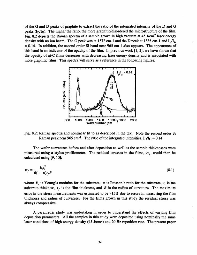
of the G and D peaks of graphite to extract the ratio of the integrated intensity of the D and G peaks (loIIG)' The higher the ratio, the more graphitic/disordered the microstructure of the film. Fig. 8.2 depicts the Raman spectra of a sample grown in high vacuum at 45 J/cm2 laser energy density with no ion beam. The G peak was at 1572 cm-1 and the D peak at 1385 cm-1 and IoIIG =0.14. In addition, the second order Si band near 965 cm-1 also appears. The appearance of this band is an indicator of the opacity of the film. In previous work [1, 2], we have shown that the opacity of at-C films decreases with decreasing laser energy density and is associated with more graphitic films. This spectra will serve as a reference in the following figures.
800 1000 1200 1400 1600-1) 1800 2000 Wavenumber (em
Fig. 8.2: Raman spectra and nonlinear fit to as described in the text. Note the second order Si Raman peak near 965 cm-I . The ratio of the integrated intensities, Inflo =0.14.
The wafer curvatures before and after deposition as well as the sample thicknesses were measured using a stylus profilometer. The residual stresses in the films, GI , could then be calculated using [9, 10]:
(8.1)
where Es is Young's modulus for the substrate, v is Poisson's ratio for the substrate, ts is the substrate thickness, tI is the film thickness, and R is the radius of curvature. The maximum
error in the stress measurements was estimated to be -15% due to errors in measuring the film thickness and radius of curvature. For the films grown in this study the residual stress was always compressive.
A parametric study was undertaken in order to understand the effects of varying film deposition parameters. All the samples in this study were deposited using nominally the same laser conditions of high energy density (45 J/cm2) and 20 Hz repetition rate. The present paper
34

focuses on the changes in residual stress and in the Raman spectra as a function of the ion beam deposition parameters.
Figs. 8.3a and 8.3b depict representative Raman spectra taken from films grown with Ar and 50% N21Ar ion beams respectively of constant current density (J =260 J.1A1cm2) and varying ion beam voltages. In general, as the ion beam voltage increases, the Raman spectra (Figs. 8.3a, 8.3b) become increasingly asymmetric. The peak position of the G peak shifts downward in wavenumber from -1570 to 1545 cm- I , and the second order Si Raman band disappears indicating that the opacity of the films increases. All these changes are indicative of a more disordered and graphitic-like change in the film structure. The ion bombardment seems to be reducing the diamond-like character of the films. On closer examination of Figs. 8.3a and 8.3b, it appears that the D peak for the 50% N 21Ar samples appears to be larger in intensity at the lower voltages (200 - 5OOV) than for the pure Ar ion beam samples (Fig. 3b). At the high ion voltage the disorder peak appears greater for the pure argon ion beam than for the 50% N2/Ar samples.
The disorder peak for the pure argon beam increases almost linearly with ion voltage. Whereas, in the case of the nitrogen ion beam the disorder peak rises more quickly with voltage. Having higher mass than nitrogen ions, argon ions should be creating more displacements in the growing films and thus greater disorder resulting in a more intense D peak at a given current density. However; if nitrogen is incorporated into the samples, then C-N bonding could account for the extra intensity in the disorder peak since this mode should appear near 1380 cm-l.[ll] The at-C structure may not be modified as much as the spectra indicate at the low voltages, as nitrogen incorporation could account for the extra intensity in the disorder peak.
800 1000 1200 1400 1600 1800 2000 800 1000 1200 1400 1600 1800 2000
Wavenumber (cm -1) Wavenumber (cm -1)
Fig. 8.3: Raman intensity vs. wavenumber and beam voltage at Ib = 260 J.1A1cm2 in a.) 0% N2
and b.) 50% N2 in Ar.
35

Fig. 8.4 is a compilation of the residual stress and integrated intensity ratios as a function of ion beam voltage for varying feed gas compositions at constant current density (J = 260 IlAlcm2). In general, we see that the residual stress decreases and the disorder peak increases with ion voltage. If the residual stress in the films is an indication of the relative sp3 bonding content then the ion bombardment is serving to reduce the sp3/sp2 ratio.
8
6
-&! 4
"-II) 2., !
CiS 0
-2 ~__________________________~~o
0 500 1000 1500 Ion Voltage (V)
Fig. 8.4 Residual compressive stress and integrated intensity ratio vs. ion voltage at varying N2 to Ar gas feed ratios.
Elastic recoil detection measurements made on these films show that samples grown in a >50% N2/Ar feed gas have -30% incorporated nitrogen. Others have reported n-type semiconducting behavior in at-C films doped with < 1 % nitrogen. At higher doping levels, the at-C structure is significantly changed and the fum is no longer insulating.
Fig. 8.5 depicts representative Raman spectra taken from films grown in an Argon ion beam of 200 V at varying current density. Fig. 8.6 depicts the residual stress and peak intensity ratios for these films, and for samples grown in 10% nitrogen in argon. The residual stress and the intensity ratio are inversely correlated as before, but the increase in current density has less of an effect on the magnitude of the D peak. This indicates that the film bonding is less affected by current density than by the ion voltage. The addition of 10% nitrogen to the feed gas has little effect on the disorder peak and residual stress levels. The changes in the spectra with ion voltage are much more dramatic. The reason for this behavior is not understood. In general, ions of higher energy (voltage) will penetrate deeper into the surface of the growing films and produce more damage than lower energy ions. But, an increase in the current density ought to produce proportionally more damage as well, unless there is another mechanism for limiting the ion damage above a certain current level. Since the Raman spectra here do not directly probe the sp3-bonded atoms in the film, it may be that the sp3-bonded portions of the structure are less effected at low ion voltages. The increase in the disorder peak with voltage would then be attributed to the breakdown of sp3 bonds and structures at these higher ion energies.
36

720 pAfcm2
800 1000 1200 1400 1600 1800 2000 Wavenumber (em -1)
Fig. 8.5: Raman intensity vs. wavenumber and beam current at Vb = 200 V in Ar.
10 10 N/(N
2 + Ar) I = 260 J,1AIcm2
b 8 --e- O.O Vb= 200 V 8
- -.-0.1 Bas
a.6 ..6a.CJ g-en G)en
!4 ..
4a.- G)U)
2
~
0 0 0 100 200 300 400 500 600 700
Current Density (J =IJA)
Fig. 8.6: Stress and integrated intensity ratio versus ion current.
Ion-assisted pulsed laser deposition can be used to dope nitrogen into at-C films. We find that nitrogen can be added to the films at moderate beam voltage and current levels with minor changes to the Raman spectra and small reductions in the residual compressive stress. Higher currents and voltages lead to more intense disorder peaks and correlate with reduced residual stress. At a given ion voltage, the intensity of the D Raman peak varies only slightly with increased ion current density and/or nitrogen content of the ion feed gas. These results indicate that the ion beam is inducing greater disorder in the films and reducing the sp3/sp2 bonding ratio in the films.
37

References
1. M. J. Siegal, T. A. Friedmann, S. R. Kurtz, D. R. Tallant, R. L. Simpson, F. Dominguez, and K. F. McCarty, in Novel Forms of Carbon II, edited by C. L. Renschler, D. Cox, J. Pouch, and Y. Achiba (Materials Research Society, Pittsburgh, 1994), Vol. .
2. T. A. Friedmann, M. P. Siegal, D. R. Tallant, R. L. Simpson, and F. Dominguez, in Novel Forms ofCarbon II, edited by C. L. Renschler, D. Cox, J. Pouch, and Y. Achiba (Materials Research Society, Pittsburgh, 1994), Vol. 349,.
3. C. A. Davis, Y. Yin, D. R. McKenzie, L. E. Hall, E. Kravtchinskaia, V. Keast, G. A. J. Amaratunga, and V. S. Veerasamy2: Non-Cryst. Solids 170,46 (1994). r!lc....s:g
4. V. S. Veerasamy, G. A. J. Amaratunga, J. S. Park; W. I. Milne, H. S. MacKenzie, and D. R. McKenzie, Appl. Phys. Lett. 64,2297 (1994). ftff(./t'
5. G. S. Higashi, Y. J. Chabal, G. W. Trucks, and K. Raghavacharl, Appl. Phys. Lett. 56,656 (1990).
6. M. Yoshikawa, G. Katagiri, H. Ishida, and A. Ihitani, Appl. Phys. Lett. 52, 1639 (1988). 7. J. Wagner, C. Wild, and P. Koidl, Appl. Ph~ Lett. 591 779 (1991). 8. M. Ramsteiner and J. Wagner, AppT.phV;: Leit. ~i: 1355 (19~jr. 9. R. W. Hoffman, Phys. Thin FUm; 3, 2'1 (966). 10. u. A. Brantley,! Ann] pbJ(S 44, ~J4 (]9W",-,J'IJPl· A 11. M. Y. Chen, D. Li, X. Lin, V. P. Dravid, Y. W. Chung, M. S. Wong, and W. d. Sproul, J.
Y.f!:c. Sc!.:_~~c¥~1A.,llt~~~~ "JV S T A
38

IX. Summary
This project set out to identify a process to develop diamond and/or diamond-like carbon films for electronic applications. Great strides were made with the invention of the use of a cubic boron nitride (c-BN) template layer for the growth of diamond films by chemical vapor deposition (CVD). This template technique directly addresses a critical problem in the growth of diamond films, the typically low nucleation density of diamond grains on a growth surface. Due to the isotropic growth properties of diamond, a low nucleation density of growth requires very thick films be grown in order for diamond grains to coalesce and cover an entire surface. Traditional means to accomplish this result involve the use of diamond grit to mechanically scratch the surface of a given substrate, such as Si, for the creation of nucleation sites. Such damage of a semiconductor substrate surface is unacceptable for use in microelectronics.
c-BN films are grown on untreated Si surfaces using ion-assisted pulsed-laser deposition (PLD). The structural and chemical similarities between c-BN and diamond suggest potential compatibility. Since the c-BN films are nanocrysta1line, there exists a high density of nucleation sites for CVD diamond film growth. Unfortunately, while a promising breakthrough for the growth of small-grain, relatively thin diamond films that provide complete surface coverage of a substrate, such films are still too coarse for real use in microelectronics.
Diamond-like carbon (OLC) films appear to have many of the necessary morphological properties absent in diamond films. DLC films consist of amorphous carbon networks with both sp2 (graphite-like) and sp3 (diamond-like) bonding. A high concentration of hydrogen is present in these materials resulting from CVD growth processes using hydrocarbon gases. The hydrogen appears necessary to terminate dangling bonds and provide stabilization for sp3 bonding. DLC films conform to most surfaces and provide complete coverage after only a few monolayers of growth. Both semiconducting and insulating properties have been measured. Unfortunately, the semiconducting properties are poor at best. This eliminates DLC for use as an active device layer in microelectronics. However, while the insulating properties are not as good as those of diamond either, the dielectric permittivity is low enough to be considered for further development as passive intermetallic dielectrics in lieu of Si02. Nevertheless, DLC films will never be used in this application due to a very simple deficiency. The terminating hydrogen atoms are not stable in these bonding configurations at temperatures above - 300·C. Since nearly all microelectronic device development requires temperature processing to - 50(YC, the DLe films will change character. Thermally processed films will have a higher concentration of sp2 bonding, yielding lower resistivities and higher dielectric constants.
Energetic physical deposition processes such as PLO can be used to grow diamond-like carbon films in the absence of hydrogen. These hydrogen-free DLC materials are referred to as amorphous tetrahedral DLC, or a-tC. The energetics of deposition appear to provide the necessary conditions for sp3 C-C bonding. a-tC films appear to have many of the properties of hydrogenated DLC; high hardness, smooth morphology, and high electrical resistivity. In addition, by controlling the energetics of 'the PLD process, it is possible to control the electrical
39

resistivity over several orders of magnitude. In addition, a-tC is stable to temperatures approaching 800·C in inert ambients (vacuum, argon). However, the dielectric permittivity of atC is typically close to that of diamond, about twice that of Si02.
There are structural differences between hydrogenated OLC and a-tC that likely account for the difference in dielectric permittivity. X-ray reflection experiments used to measure the density of a-tC films finds that it is - 3 glcm3. OLC typically is measured near 2 g/cm3. The density of diamond is 3.55 glcm3• Generally, higher the density of a given material, the higher its permittivity. So it should not be surprising to fmd that high density a-tC has a permittivity significantly higher than that of low density OLC. Low density a-tC is too conductive to be used as a dielectric material. This is likely due to the relatively high content of sp2 C-C bonding in this material.
This LDRD project has also studied the growth of a-tC films under conditions which both passively and actively contribute dopants or impurities into the system. PLO growth in gas ambients such as argon, hydrogen and nitrogen has been studied. Argon, a noble gas, does not react with carbon, rather its presence in the growth atmosphere acts to attenuate the kinetic energy of the laser ablated carbon species. Films grown in this manner are similar to a-tC films grown by PLO in a vacuum ambient with less laser power density. Ambients containing hydrogen lead to films similar to hydrogenated OLC. The use of nitrogen is perhaps the most interesting. Nitrogen-containing a-tC films tend to be less electrically resistive, less thermally stable, softer, less optically transparent, and have low density. Use of an ion beam to simultaneously impinge upon a substrate with the ablated species leads to a different set of results. Essentially, a-tC films grown with ion beams of either argon or nitrogen result in low resistance, optically opaque properties. Interestingly, the nitrogen content achievable by both techniques (background gas and nitrogen ion bombardment, is the same at (N atoms)/(C atoms) 0.30.
It would appear that the physical, chemical, and electrical properties of diamond or forms of OLC are insufficient for active use in microelectronics or passive use as intermetallic dielectrics. However, there are still important applications within microelectronics that these materials could impact. The high-temperature stability and relative chemical inertness of a-tC films suggests potential use as encapsulants for environmental protection. The good optical transparency and high-hardness of the films are desirable for protective coatings for laser windows and other optics. The mechanical properties could provide ultrahard coatings for integrated micro-electro-mechanical machines (IMEMs) as well as machine tools.
Finally, carbon materials have been used for many years for electron emission sources in defense program related switch tube components. This same property is being pursued through other programs at both Sandia and other laboratories for use in novel designs for electronemission based flat panel displays and low-cost, energy-efficient, environmentally-friendly light bulbs. This electronic property of carbon films, such as a-tC, is closely related to the C-C atomic bonding structures, gross morphology, and electronic (resistivity, permittivity) properties. The
40

development of carbon films for these applications has proceeded despite the lack of a true fundamental understanding of the correlation between electron emission and other measurable properties of carbon materials.
This project has demonstrated the need for a fundamental understanding of the relationship between growth energetics, atomic structures, and materials properties. While it has been possible to grow a-tC films and achieve some tailoring of their properties via growth energetics, their full potential has yet to be realized. Moreover, a fundamental understanding of the relationship between local bonding structures and measurable properties is virtually nonexistent. The difficulty is due to the low-atomic weight and the lack of crystallinity in a-tC. There presently exists a need for first-principles theoretical calculations to determine representative atomic structures so as to relate bonding structures with measurable properties. The development of such an understanding of materials properties based upon knowledge of realistic bonding geometries should ultimately enable the design of engineered materials for specific applications.
The earlier research in this LDRD project centered around the development of improved growth methods for CVD diamond films is important. It is true that this work has not greatly improved the likelihood of diamond fums being used in conjunction with silicon-based, active microelectronic devices. However, the development of the c-BN template method for increasing the density of diamond grain nucleation sites has led to the growth of continuous, full surface coverage diamond films that can be significantly thinner than films grown without templates and without the need for severe surface damage. Diamond coating technologies are prevalent in many industrial applications, several of which could be positively impacted by this development.
Future research programs should be able to build upon the successes of this LDRD project. These include the ability to grow a-tC films over large-area substrates at low temperatures using PLD. The energetics of deposition can be used to tailor the material properties. Many of these properties, such as resistivity, permittivity, optical transparency, film stress, density and temperature stability have been measured and correlated with growth conditions. Applicationsdriven projects such as developing ultra-hard coatings for wear-resistance, or electron-emission properties for switch tubes, displays and light bulbs require this information.
41

Distribution:
1 MS-1436 C. E. Meyers, 1007 1 MS-1427 P.L.Mattern, 1100 1 MS-1421 E. B. Stechel, 1153 , ,10 MS-1421 M. P. Siegal, 1153 1 MS-1421 T. A. Friedmann, 1153 1 MS-1421 J. P. Sullivan, 1153 1 MS-1421 J. Mikkalson, 1153 1 MS-1421 F. Dominguez, 1153 1 MS-1411 D. R. Tallant, 1823 1 MS-1411 R. L. Simpson, 1823 1 MS-9161 K.F.McCarty, 8716 1 MS-9053 L. Bernardez, 8362 1 MS-9161 D. Dibble, 8716 1 MS-9161 P. B. Mirkarimi, 8716 1 MS-9018 Central Tech Files, 8523-2 5 MS-0899 Technical Library, 4414 1 MS-0619 Print Media, 12615 2 MS-OI00 Document Processing, 7613-2 44 DOE/OSTI
42


![SOME IMPORTANT POINTS - prepareforchemistryprepareforchemistry.weebly.com/uploads/1/2/1/7/12175355/789-p... · Web view... (NH3)5Cl]Cl2 = Pentaamminechloridocobalt(III) chloride](https://img.pdfslide.us/doc/110x75/5a9e9e6e7f8b9a0d158b9d5a/docsome-important-points-prepareforchemistr-view-nh35clcl2-pentaamminechloridocobaltiii.jpg)