Embed Size (px)
Citation preview

1 of 23
Proprietary and Confidential
GS3440 Adaptive Cable EqualizerFinal Data SheetRev. 2 December 2012
Extended Reach 3G/HD/SD Adaptive Cable Equalizer
GS3440
www.semtech.com
Key Features• SMPTE ST 424, SMPTE ST 292 and SMPTE ST 259
compliant
• Automatic cable equalization
• Multi-standard operation from 125Mb/s to 2.97Gb/s
• Performance optimized for 270Mb/s, 1.485Gb/s and 2.97Gb/s. Typical equalized length of Belden 1694A cable up to:
210m at 2.97Gb/s
300m at 1.485Gb/s
550m at 270Mb/s
• Supports DVB-ASI at 270Mb/s
• Supports MADI at 125Mb/s
• Manual bypass (useful for low data rates with slow rise/fall times)
• Programmable carrier detect with squelch threshold adjustment
• Automatic power-down on loss of signal
Standby power <35mW (typical)
• Differential output supports DC-coupling from 1.2V to 3.3V CML logic
• Option to compensate for 6dB flat attenuation prior to input of device
• Selectable output de-emphasis: 2dB, 4dB and 6dB
• Standard EIA/JEDEC logic control and status signal levels
• Single 3.3V power supply operation
• 180mW power consumption (typical)
• Wide operating temperature range of -40ºC to +85ºC
• Small footprint QFN package (4mm x 4mm)
Footprint compatible with the GS2974A, GS2974B, GS2984 and GS2994
• Pb-free and RoHS compliant
Applications• SMPTE ST 424, SMPTE ST 292 and SMPTE ST 259
coaxial cable serial digital interfaces
DescriptionThe GS3440 is a high-speed BiCMOS device designed to equalize and restore signals received over 75Ω coaxial cable.
The device is designed to support SMPTE ST 424, SMPTE ST 292 and SMPTE ST 259, and is optimized for performance at 270Mb/s, 1.485Gb/s and 2.97Gb/s.
The GS3440 features DC restoration to compensate for the DC content of SMPTE pathological signals.
The Carrier Detect output pin (CD) indicates whether an input signal has been detected. It can be connected directly to the SLEEP pin to enable automatic sleep on loss of carrier.
A voltage programmable threshold, set via the SQ_ADJ pin, forces CD high when the input signal amplitude falls below the threshold. This allows the GS3440 to distinguish between low-amplitude SDI signals and noise at the input of the device.
The equalizing and DC restore stages are disengaged and no equalization occurs when the BYPASS pin is HIGH. Setting the BYPASS pin HIGH is useful for signals launched at the signal source with low data rates and/or slow rise/fall times.
The GS3440 features a gain selection pin (GAIN_SEL) which can be used to compensate for 6dB flat attenuation prior to the input of the device.
The differential output can be DC-coupled to Semtech’s reclockers and cable drivers, as well as industry-standard 1.2V, 1.8V, 2.5V and 3.3V CML logic by changing the voltage applied to the VCC_O pin. In general, DC-coupling to any termination voltage between 1.2V and 3.3V is supported.
The GS3440 also features programmable output de-emphasis with three, user-selectable operating levels to support long PCB traces at the output of the device.
GS3440 Adaptive Cable EqualizerFinal Data SheetRev. 2 December 2012
2 of 23
Proprietary and Confidential
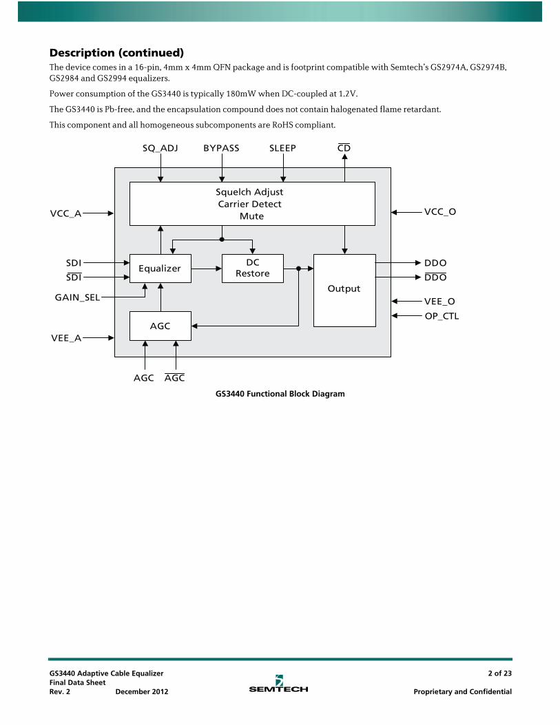
Description (continued)The device comes in a 16-pin, 4mm x 4mm QFN package and is footprint compatible with Semtech’s GS2974A, GS2974B, GS2984 and GS2994 equalizers.
Power consumption of the GS3440 is typically 180mW when DC-coupled at 1.2V.
The GS3440 is Pb-free, and the encapsulation compound does not contain halogenated flame retardant.
This component and all homogeneous subcomponents are RoHS compliant.
GS3440 Functional Block Diagram
Equalizer
Output
AGC
SDI
SLEEP
DDO
BYPASS CD
SDI DDO
AGCAGC
SQ_ADJ
Squelch AdjustCarrier Detect
Mute
DCRestore
VCC_O
VEE_O
OP_CTL
VCC_A
VEE_A
GAIN_SEL
GS3440 Adaptive Cable EqualizerFinal Data SheetRev. 2 December 2012
3 of 23
Proprietary and Confidential
Contents
Key Features ........................................................................................................................................................1
Applications.........................................................................................................................................................1
Description...........................................................................................................................................................1
Description (continued) ...................................................................................................................................2
1. Pin Out...............................................................................................................................................................4
1.1 GS3440 Pin Assignment .................................................................................................................4
1.2 GS3440 Pin Descriptions ................................................................................................................4
2. Electrical Characteristics ............................................................................................................................7
2.1 Absolute Maximum Ratings ..........................................................................................................7
2.2 DC Electrical Characteristics ........................................................................................................7
2.3 AC Electrical Characteristics ........................................................................................................9
3. Input/Output Circuits ............................................................................................................................... 11
4. Detailed Description.................................................................................................................................. 13
4.1 Serial Digital Inputs ...................................................................................................................... 13
4.2 Automatic (Adaptive) Cable Equalization ............................................................................. 13
4.3 Differential Digital Data Output ............................................................................................... 13
4.4 Programmable Squelch Adjust (SQ_ADJ) .............................................................................. 14
4.5 Carrier Detect, Sleep, and Auto-Sleep .................................................................................... 14
4.6 GAIN_SEL ......................................................................................................................................... 15
4.7 Adjustable Output Swing, De-Emphasis and Mute ............................................................ 15
5. Application Information .......................................................................................................................... 17
5.1 High-Gain Adaptive Cable Equalizers .................................................................................... 17
5.2 PCB Layout ....................................................................................................................................... 17
5.3 Typical Application Circuit ........................................................................................................ 18
6. Package & Ordering Information .......................................................................................................... 19
6.1 Package Dimensions ..................................................................................................................... 19
6.2 Packaging Data ............................................................................................................................... 19
6.3 Recommended PCB Footprint ................................................................................................... 20
6.4 Marking Diagram ........................................................................................................................... 20
6.5 Solder Reflow Profiles .................................................................................................................. 21
6.6 Ordering Information ................................................................................................................... 21
Appendix - Relevant Documentation...................................................................................................... 21
Revision History (Document # 56482) ..................................................................................................... 22
GS3440 Adaptive Cable EqualizerFinal Data SheetRev. 2 December 2012
4 of 23
Proprietary and Confidential
1. Pin Out
1.1 GS3440 Pin Assignment
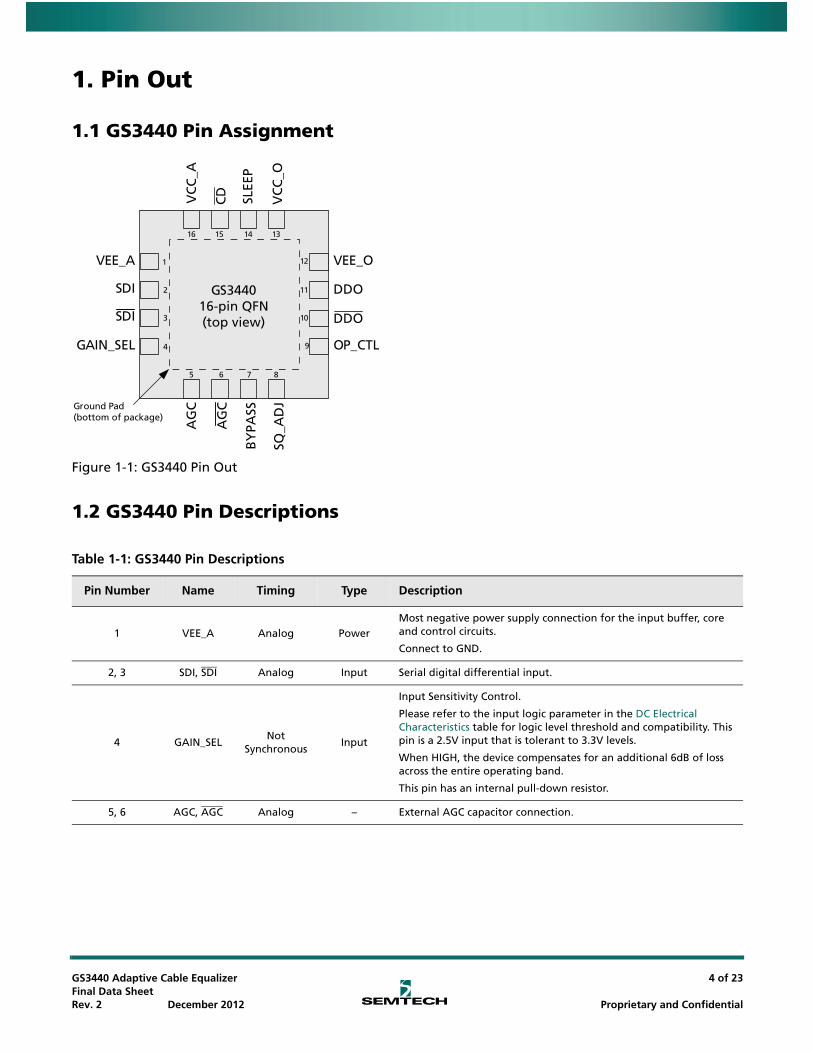
Figure 1-1: GS3440 Pin Out
1.2 GS3440 Pin Descriptions
Ground Pad(bottom of package)
GS344016-pin QFN(top view)
SQ_A
DJ
AG
C
VC
C_O
SLEE
P
VC
C_A
BY
PASS
5 6 7 8
16 15 14 13A
GC
GAIN_SEL
VEE_A
SDI
1
2
3
4
SDI
VEE_O
DDO
DDO
OP_CTL
12
11
10
9
CD
Table 1-1: GS3440 Pin Descriptions
Pin Number Name Timing Type Description
1 VEE_A Analog PowerMost negative power supply connection for the input buffer, core and control circuits.
Connect to GND.
2, 3 SDI, SDI Analog Input Serial digital differential input.
4 GAIN_SELNot
SynchronousInput
Input Sensitivity Control.
Please refer to the input logic parameter in the DC Electrical Characteristics table for logic level threshold and compatibility. This pin is a 2.5V input that is tolerant to 3.3V levels.
When HIGH, the device compensates for an additional 6dB of loss across the entire operating band.
This pin has an internal pull-down resistor.
5, 6 AGC, AGC Analog – External AGC capacitor connection.
GS3440 Adaptive Cable EqualizerFinal Data SheetRev. 2 December 2012
5 of 23
Proprietary and Confidential
7 BYPASSNot
SynchronousInput
Core Bypass Control.
Please refer to the input logic parameter in the DC Electrical Characteristics table for logic level threshold and compatibility. This pin is a 2.5V input that is tolerant to 3.3V levels.
Forces the equalizer and DC-restore stages into Bypass mode when HIGH. No equalization occurs in this mode.
This pin has an internal pull-down resistor.
8 SQ_ADJ Analog Input
Squelch Threshold Adjust.
Adjusts the input signal amplitude threshold of the carrier detect function. The serial data output of the device can be muted when the serial data input signal amplitude is too low by connecting the CD and OP_CTL pins using a suitable resistor network (see Figure 4-2 and Figure 4-3).
This pin has an internal pull-down resistor.
Note: The SQ_ADJ function is only available when the device is not in auto-sleep mode. Reference Section 4.5 for more detail.
9 OP_CTLNot
SynchronousInput
Controls the Output Swing, De-emphasis and Mute Features of the DDO/DDO outputs.
When this pin is connected to GND, the output swing is 850mVppd with no de-emphasis applied to the output signal.
With this pin connected to 2.5V, the output is muted.
Intermediate voltages and functions are shown in Table 4-5. These voltages can be achieved as shown in Figure 4-2 and Figure 4-3.
This pin has an internal pull-down resistor.
10, 11 DDO, DDO Analog Output Serial digital differential output.
12 VEE_O Analog PowerMost negative power supply connection for the output buffer.
Connect to GND.
13 VCC_O Analog PowerMost positive power supply connection for the output buffer.
Connect to 1.2V - 3.3V DC.
14 SLEEPNot
SynchronousInput
SLEEP Control.
Please refer to the input logic parameter in the DC Electrical Characteristics table for logic level threshold and compatibility. This pin is a 2.5V input that is tolerant to 3.3V levels.
When HIGH the part is powered-down except for the Carrier Detect function.
This pin can be connected directly to the CD pin to automatically put the device to sleep (low-power operation) on loss of carrier.
This pin has an internal pull-down resistor.
Note: When SLEEP is connected to CD for automatic power reduction on loss of carrier, the SQ_ADJ pin will not modify the CD threshold. The CD threshold will revert to the default value used when SQ_ADJ is pulled LOW.
Table 1-1: GS3440 Pin Descriptions (Continued)
Pin Number Name Timing Type Description
GS3440 Adaptive Cable EqualizerFinal Data SheetRev. 2 December 2012
6 of 23
Proprietary and Confidential
15 CDNot
SynchronousOutput
Carrier Detect Status Output.
Please refer to the output logic parameter in the DC Electrical Characteristics table for logic level threshold and compatibility. This pin is a 2.5V output.
Indicates presence of an input signal. When the CD pin is LOW, a signal has been detected at the input. When this pin is HIGH, this indicates loss of input signal.
16 VCC_A Analog PowerMost positive power supply connection for the input buffer, core and control circuits.
Connect to +3.3V DC.
– Center Pad – PowerInternally bonded to VEE_A.
Connect to GND with at least 5 VIAs.
Table 1-1: GS3440 Pin Descriptions (Continued)
Pin Number Name Timing Type Description
GS3440 Adaptive Cable EqualizerFinal Data SheetRev. 2 December 2012
7 of 23
Proprietary and Confidential
2. Electrical Characteristics
2.1 Absolute Maximum Ratings
2.2 DC Electrical Characteristics
Table 2-1: Absolute Maximum Ratings
Parameter Value
Supply Voltage - Core/Output Driver -0.5V to +3.6V DC
Input ESD Voltage (HBM) 5kV
Storage Temperature Range (Ts) -50°C to 125°C
Input Voltage Range (any input) -0.3 to (VCC_A +0.3)V
Operating Temperature Range -40°C to +85°C
Solder Reflow Temperature 260°C
Note: Absolute Maximum Ratings are those values beyond which damage may occur. Functional operation outside of the ranges shown in Table 2-1 is not implied.
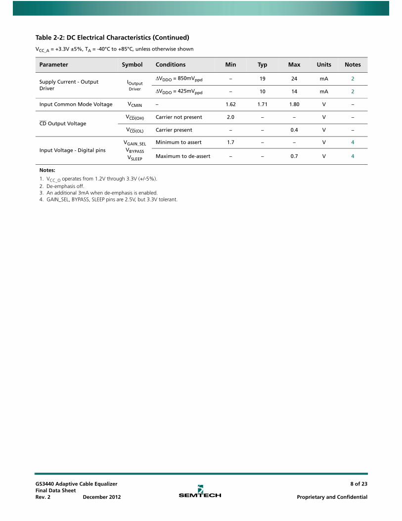
Table 2-2: DC Electrical Characteristics
VCC_A = +3.3V ±5%, TA = -40°C to +85°C, unless otherwise shown
Parameter Symbol Conditions Min Typ Max Units Notes
Supply Voltage - Core VCC_A – 3.135 3.3 3.465 V –
Supply Voltage - Output Driver
VCC_O
– 1.14 1.2 1.26 V 1
– 2.375 2.5 2.625 V 1
– 3.135 3.3 3.465 V 1
Power Consumption PD
VCC_O = 1.2V ΔVDDO = 425mVppd
– 180 215 mW 2
VCC_O = 1.2V ΔVDDO = 850mVppd
– 195 230 mW 2
VCC_O = 2.5V ΔVDDO = 425mVppd
– 196 231 mW 2
VCC_O = 2.5V ΔVDDO = 850mVppd
– 221 261 mW 2
VCC_O = 3.3V ΔVDDO = 425mVppd
– 202 242 mW 2
VCC_O = 3.3V ΔVDDO = 850mVppd
– 240 283 mW 2
Supply Current - Core Is – – 53 59 mA 2, 3
GS3440 Adaptive Cable EqualizerFinal Data SheetRev. 2 December 2012
8 of 23
Proprietary and Confidential
Supply Current - Output Driver
IOutput Driver
ΔVDDO = 850mVppd – 19 24 mA 2
ΔVDDO = 425mVppd – 10 14 mA 2
Input Common Mode Voltage VCMIN – 1.62 1.71 1.80 V –
CD Output VoltageVCD(OH) Carrier not present 2.0 – – V –
VCD(OL) Carrier present – – 0.4 V –
Input Voltage - Digital pins
VGAIN_SEL
VBYPASSVSLEEP
Minimum to assert 1.7 – – V 4
Maximum to de-assert – – 0.7 V 4
Notes:
1. VCC_O operates from 1.2V through 3.3V (+/-5%).2. De-emphasis off.3. An additional 3mA when de-emphasis is enabled.4. GAIN_SEL, BYPASS, SLEEP pins are 2.5V, but 3.3V tolerant.
Table 2-2: DC Electrical Characteristics (Continued)
VCC_A = +3.3V ±5%, TA = -40°C to +85°C, unless otherwise shown
Parameter Symbol Conditions Min Typ Max Units Notes
GS3440 Adaptive Cable EqualizerFinal Data SheetRev. 2 December 2012
9 of 23
Proprietary and Confidential
2.3 AC Electrical Characteristics
Table 2-3: AC Electrical Characteristics
VCC_A = +3.3V ±5%, TA = -40°C to +85°C, unless otherwise shown
Parameter Symbol Conditions Min Typ Max Units Notes
Serial input data rate DRDDO – 125 – 2970 Mb/s 1
Input Voltage Swing ΔVSDI
Differential, 270Mb/s and 1.485Gb/s
720 800 950 mVppd 2
Differential, 2.97Gb/s
720 800 880 mVppd 3
Output Voltage Swing ΔVDDO
100Ω load, differential, OP_CTL set for high swing
700 850 1000 mVppd –
100Ω load, differential, OP_CTL set for low swing
350 425 500 mVppd –
Output Jitter at Various Cable Lengths and Data Rates
–2.97Gb/s Belden 1694A: 0-120m
– – 0.25 UI 3, 4, 5
–2.97Gb/s Belden 1694A: 120-150m
– – 0.3 UI 3, 4, 5
–2.97Gb/s Belden 1694A: 150-170m
– – 0.4 UI 3, 4, 5
–2.97Gb/s Belden 1694A: 170-200m
– – 0.5 UI 3, 4, 5
–2.97Gb/s Belden 1694A: 200-210m
– 0.5 – UI 3, 4, 5
–1.485Gb/s Belden 1694A: 0-200m
– – 0.2 UI 3, 4, 5
–1.485Gb/s Belden 1694A: 200-260m
– – 0.3 UI 3, 4, 5
–1.485Gb/s Belden 1694A: 260-300m
– 0.3 – UI 3, 4, 5
–270Mb/s Belden 1694A: 0-300m
– 0.1 0.15 UI 3, 4, 5
–270Mb/s Belden 1694A: 300-500m
– – 0.25 UI 3, 4, 5
270Mb/s Belden 1694A: 500-550m
– 0.25 – UI 3, 4, 5
Output Rise/Fall time
–2.97Gb/s & 1.485Gb/s 20% - 80%
– 75 – ps –
–270Mb/s
20% - 80%– 150 – ps –
Mismatch in rise/fall time – – – – 30 ps –
GS3440 Adaptive Cable EqualizerFinal Data SheetRev. 2 December 2012
10 of 23
Proprietary and Confidential
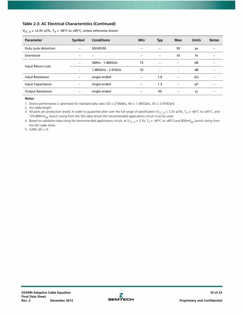
Duty cycle distortion – SD/HD/3G – – 30 ps –
Overshoot – – – – 10 % –
Input Return Loss– 5MHz - 1.485GHz 15 – – dB –
– 1.485GHz - 2.97GHz 10 – – dB –
Input Resistance – single-ended – 1.9 – kΩ –
Input Capacitance – single-ended – 1.3 – pF –
Output Resistance – single-ended – 50 – Ω –
Notes:
1. Device performance is optimized for standard data rates (SD = 270Mb/s, HD = 1.485Gb/s, 3G = 2.970Gb/s)2. 0m cable length.3. All parts are production tested. In order to guarantee jitter over the full range of specification (VCC_A = 3.3V ±5%, TA = -40°C to +85°C, and
720-880mVpp launch swing from the SDI cable driver) the recommended applications circuit must be used.4. Based on validation data using the recommended applications circuit, at VCC_A = 3.3V, TA = -40°C to +85°Cand 800mVpp launch swing from
the SDI cable driver.5. GAIN_SEL = 0.
Table 2-3: AC Electrical Characteristics (Continued)
VCC_A = +3.3V ±5%, TA = -40°C to +85°C, unless otherwise shown
Parameter Symbol Conditions Min Typ Max Units Notes
GS3440 Adaptive Cable EqualizerFinal Data SheetRev. 2 December 2012
11 of 23
Proprietary and Confidential
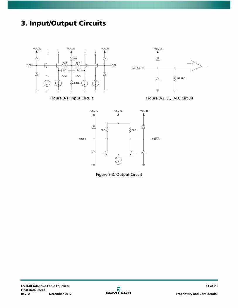
3. Input/Output Circuits
Figure 3-1: Input Circuit Figure 3-2: SQ_ADJ Circuit
Figure 3-3: Output Circuit
2.625kΩ
RC
SDI SDI
RC
2kΩ
2kΩ
2kΩ
VCC_AVCC_A VCC_A
SQ_ADJ
82.4kΩ
+
-
VCC_A
50Ω50Ω
DDODDO
VCC_OVCC_O VCC_O
GS3440 Adaptive Cable EqualizerFinal Data SheetRev. 2 December 2012
12 of 23
Proprietary and Confidential
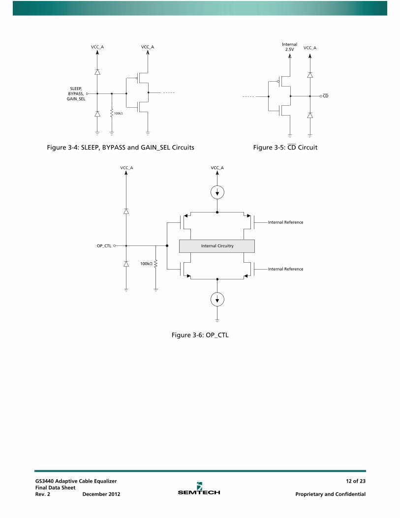
Figure 3-4: SLEEP, BYPASS and GAIN_SEL Circuits Figure 3-5: CD Circuit
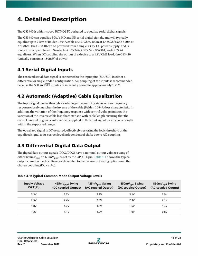
Figure 3-6: OP_CTL
SLEEP,BYPASS,
GAIN_SEL
100kΩ
VCC_AVCC_A
CD
Internal2.5V VCC_A
VCC_A
Internal Reference
Internal Reference
OP_CTL Internal Circuitry
100kΩ
VCC_A
GS3440 Adaptive Cable EqualizerFinal Data SheetRev. 2 December 2012
13 of 23
Proprietary and Confidential
4. Detailed Description
The GS3440 is a high-speed BiCMOS IC designed to equalize serial digital signals.
The GS3440 can equalize 3Gb/s, HD and SD serial digital signals, and will typically equalize up to 210m of Belden 1694A cable at 2.97Gb/s, 300m at 1.485Gb/s, and 550m at 270Mb/s. The GS3440 can be powered from a single +3.3V DC power supply, and is footprint-compatible with Semtech’s GS2974A, GS2974B, GS2984, and GS2994 equalizers. When DC coupling the output of a device to a 1.2V CML load, the GS3440 typically consumes 180mW of power.
4.1 Serial Digital InputsThe received serial data signal is connected to the input pins (SDI/SDI) in either a differential or single-ended configuration. AC-coupling of the inputs is recommended, because the SDI and SDI inputs are internally biased to approximately 1.71V.
4.2 Automatic (Adaptive) Cable EqualizationThe input signal passes through a variable gain equalizing stage, whose frequency response closely matches the inverse of the cable (Belden 1694A) loss characteristic. In addition, the variation of the frequency response with control voltage imitates the variation of the inverse cable loss characteristic with cable length ensuring that the correct amount of gain is automatically applied to the input signal for any cable length within the supported ranges.
The equalized signal is DC-restored, effectively restoring the logic threshold of the equalized signal to its correct level independent of shifts due to AC-coupling.
4.3 Differential Digital Data OutputThe digital data output signals (DDO/DDO) have a nominal output voltage swing of either 850mVppd or 425mVppd, as set by the OP_CTL pin. Table 4-1 shows the typical output common mode voltage levels related to the two output swing options and the chosen coupling (DC vs. AC).
Table 4-1: Typical Common Mode Output Voltage Levels
Supply Voltage (VCC_O)
425mVppd Swing (DC-coupled Output)
425mVppd Swing (AC-coupled Output)
850mVppd Swing (DC-coupled Output)
850mVppd Swing (AC-coupled Output)
3.3V 3.2V 3.1V 3.1V 2.9V
2.5V 2.4V 2.3V 2.3V 2.1V
1.8V 1.7V 1.6V 1.6V 1.4V
1.2V 1.1V 1.0V 1.0V 0.8V
GS3440 Adaptive Cable EqualizerFinal Data SheetRev. 2 December 2012
14 of 23
Proprietary and Confidential
4.4 Programmable Squelch Adjust (SQ_ADJ)The GS3440 features a programmable Squelch Adjust (SQ_ADJ) threshold.
This feature can be useful in applications where there are multiple input channels using the GS3440 and the maximum gain can be limited to avoid crosstalk.
The SQ_ADJ pin acts to change the threshold of the Carrier Detect (CD) pin. When the input signal drops below the threshold set by SQ_ADJ, the CD pin will be driven HIGH, indicating that there is not a valid input signal. In applications where programmable squelch adjust is not required, the SQ_ADJ pin can be left unconnected.
This feature has been designed for use in applications such as routers, where signal crosstalk and circuit noise cause the equalizer to output erroneous data when no input signal is present. The use of a Carrier Detect function with a fixed internal reference does not solve this problem, since the signal-to-noise ratio on the circuit board could be significantly less than the default signal detection level set by the on-chip reference.
Note: When using SQ_ADJ to limit the maximum gain of the GS3440, CD should not be connected to SLEEP.
4.5 Carrier Detect, Sleep, and Auto-SleepThe Carrier Detect output pin (CD) indicates the presence of a valid signal at the input of the GS3440. When CD is LOW, the device has detected a valid input on SDI and SDI. When CD is HIGH, the device has not detected a valid input.
The GS3440 includes a SLEEP input pin, which can be used to put the device into a low-power sleep mode, consuming less than 35mW. In this mode, the outputs are high impedance and will be pulled high by the on-chip termination. Set the SLEEP pin HIGH to place the chip in this low-power state. In this mode, the Carrier Detect output will still function to facilitate the detection of a valid serial input data signal.
Auto-Sleep is enabled by connecting CD to SLEEP. When connected, the GS3440 will automatically go into low-power sleep mode when there is a loss of Serial Digital Input signal.
Note 1: CD will only detect loss of carrier for data rates greater than 19Mb/s.
Note 2: If SQ_ADJ is being used to limit the maximum gain of the device, and the maximum cable length is exceeded when BYPASS is set LOW, the CD pin will be set to HIGH even if a carrier is present.
Note 3: If the CD pin is connected to the SLEEP pin, SQ_ADJ must be either left open, or connected to ground.
Table 4-2: SLEEP Input Table
SLEEP Function
0 The GS3440 operates normally
1The GS3440 enters low-power sleep mode. CD output remains valid
GS3440 Adaptive Cable EqualizerFinal Data SheetRev. 2 December 2012
15 of 23
Proprietary and Confidential
4.6 GAIN_SELThe GS3440 has an option of compensating for 6dB of flat attenuation prior to the equalizer.
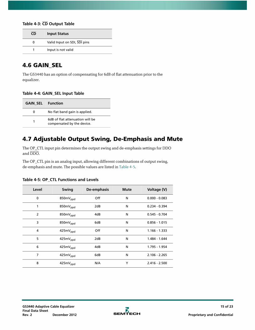
4.7 Adjustable Output Swing, De-Emphasis and MuteThe OP_CTL input pin determines the output swing and de-emphasis settings for DDO and DDO.
The OP_CTL pin is an analog input, allowing different combinations of output swing, de-emphasis and mute. The possible values are listed in Table 4-5.
Table 4-3: CD Output Table
CD Input Status
0 Valid Input on SDI, SDI pins
1 Input is not valid
Table 4-4: GAIN_SEL Input Table
GAIN_SEL Function
0 No flat band gain is applied.
16dB of flat attenuation will be compensated by the device.
Table 4-5: OP_CTL Functions and Levels
Level Swing De-emphasis Mute Voltage (V)
0 850mVppd Off N 0.000 - 0.083
1 850mVppd 2dB N 0.234 - 0.394
2 850mVppd 4dB N 0.545 - 0.704
3 850mVppd 6dB N 0.856 - 1.015
4 425mVppd Off N 1.166 - 1.333
5 425mVppd 2dB N 1.484 - 1.644
6 425mVppd 4dB N 1.795 - 1.954
7 425mVppd 6dB N 2.106 - 2.265
8 425mVppd N/A Y 2.416 - 2.500
GS3440 Adaptive Cable EqualizerFinal Data SheetRev. 2 December 2012
16 of 23
Proprietary and Confidential
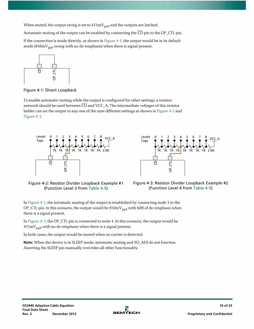
When muted, the output swing is set to 425mVppd and the outputs are latched.
Automatic muting of the output can be enabled by connecting the CD pin to the OP_CTL pin.
If the connection is made directly, as shown in Figure 4-1, the output would be in its default mode (850mVppd swing with no de-emphasis) when there is signal present.
Figure 4-1: Direct Loopback
To enable automatic muting while the output is configured for other settings, a resistor network should be used between CD and VCC_A. The intermediate voltages of this resistor ladder can set the output to any one of the nine different settings as shown in Figure 4-2 and Figure 4-3.
In Figure 4-2, the automatic muting of the output is established by connecting node 3 to the OP_CTL pin. In this scenario, the output would be 850mVppd with 6dB of de-emphasis when there is a signal present.
In Figure 4-3, the OP_CTL pin is connected to node 4. In this scenario, the output would be 425mVppd with no de-emphasis when there is a signal present.
In both cases, the output would be muted when no carrier is detected.
Note: When the device is in SLEEP mode, automatic muting and SQ_ADJ do not function. Asserting the SLEEP pin manually overrides all other functionality.
OP_
CTLCD
Figure 4-2: Resistor Divider Loopback Example #1 (Function Level 3 from Table 4-5)
Figure 4-3: Resistor Divider Loopback Example #2 (Function Level 4 from Table 4-5)
CD
OP_
CTL
VCC_A
1K 1K 1K 1K 1K 1K 1K 1K 2.6K
0 1 2 3 4 5 6 7 8LevelsTaps
CD
OP_
CTL
VCC_A
1K 1K 1K 1K 1K 1K 1K 1K 2.6K
0 1 2 3 4 5 6 7 8LevelsTaps
GS3440 Adaptive Cable EqualizerFinal Data SheetRev. 2 December 2012
17 of 23
Proprietary and Confidential
5. Application Information
5.1 High-Gain Adaptive Cable EqualizersThe GS3440 is a multi-rate adaptive cable equalizer. In order to continue to extend the cable length that the device can support, it is necessary to have high-gain in the equalizer.
A video cable equalizer must provide wide band gain over a range of frequencies in order to accommodate the range of data rates and signal patterns that are present in a SMPTE-compliant serial video stream.
Small levels of signal or noise present at the input pins of the equalizer may cause chatter at the output. In order to prevent this from happening, particular attention must be paid to board layout.
5.2 PCB LayoutSpecial attention must be paid to component layout when designing Serial Digital Interfaces for HDTV. An FR-4 dielectric can be used, however, controlled impedance transmission lines are required for PCB traces longer than approximately 1cm. Note the following PCB artwork features used to optimize performance:
• PCB trace width for 3Gb/s rate signals is closely matched to SMT component width to minimize reflections due to change in trace impedance.
• High-speed traces are curved to minimize impedance changes.
• Cutouts in the inner layers should be used under the GS3440 input and output components to minimize parasitic capacitance. For more detail on this and other layout recommendations, please refer to A Guide For Designing With Gennum’s 3G-SDI Equalizers.
GS3440 Adaptive Cable EqualizerFinal Data SheetRev. 2 December 2012
18 of 23
Proprietary and Confidential
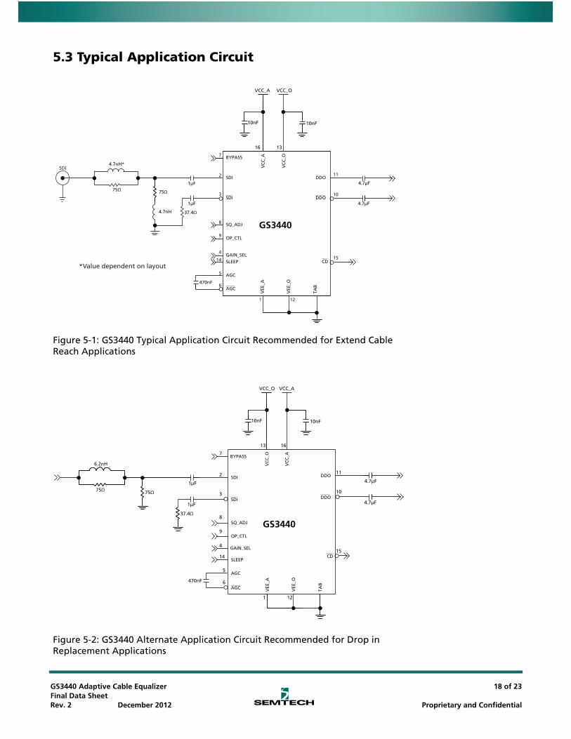
5.3 Typical Application Circuit
Figure 5-1: GS3440 Typical Application Circuit Recommended for Extend Cable Reach Applications
Figure 5-2: GS3440 Alternate Application Circuit Recommended for Drop in Replacement Applications
1
4
5
6
2
3
8
7
12
11
14 15
9
1075Ω
1µF
1µF
GS3440
37.4Ω
75Ω
4.7µF
4.7nH*
OP_CTL
DDO
DDO
SQ_ADJ
BYPASS
SDI
SDI
VC
C_A
4.7µF
470nF
TAB
CDSLEEP
VEE
_OAGC
AGC
GAIN_SEL
VEE
_A
4.7nH
SDI
*Value dependent on layout
VC
C_O
10nF
1316
10nF
VCC_A VCC_O
75Ω
6.2nH
7
10
1µF
470nF
4
14
121
13 16
8
2
3
9
11
15
6
5
37.4Ω
1µF
10nF
VCC_A
4.7µF
75Ω
VCC_O
4.7µF
GS3440OP_CTL
DDO
DDO
SQ_ADJ
BYPASS
SDI
SDI
VC
C_A
TAB
CDSLEEP
VEE
_O
AGC
AGC
GAIN_SEL
VEE
_AV
CC
_O
10nF
GS3440 Adaptive Cable EqualizerFinal Data SheetRev. 2 December 2012
19 of 23
Proprietary and Confidential
6. Package & Ordering Information
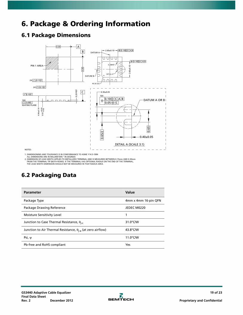
6.1 Package Dimensions
6.2 Packaging Data
4.00
4.00
A
B
C
DATUM A
DATUM B
2.60±0.10
2.60
±0.
10
0.10 M C A B
0.10 M C A B
DETAIL A
0.30@45°
R0.30 (3x)
PIN 1 AREA
0.15 C
0.15 C
0.10 C
0.08 C16X
SEATING PLANE
2X
2X
0.20
REF
0.90
±0.
10
0.02
+0.
03-0
.02
0.10 M C A B0.05 M C
0.40±0.05
0.30±0.05
DATUM A OR B
16X
0.65
0.65
/2
DETAIL A (SCALE 3:1)
NOTES:
1. DIMENSIONING AND TOLERANCE IS IN CONFORMANCE TO ASME Y14.5-1994 ALL DIMENSIONS ARE IN MILLIMETERS ° IN DEGREES2. DIMENSION OF LEAD WIDTH APPLIES TO METALLIZED TERMINAL AND IS MEASURED BETWEEN 0.15mm AND 0.30mm FROM THE TERMINAL TIP (BOTH ROWS). IF THE TERMINAL HAS OPTIONAL RADIUS ON THE END OF THE TERMINAL, THE LEAD WIDTH DIMENSION SHOULD NOT BE MEASURED IN THAT RADIUS AREA
Parameter Value
Package Type 4mm x 4mm 16-pin QFN
Package Drawing Reference JEDEC M0220
Moisture Sensitivity Level 1
Junction to Case Thermal Resistance, θj-c 31.0°C/W
Junction to Air Thermal Resistance, θj-a (at zero airflow) 43.8°C/W
Psi, ψ 11.0°C/W
Pb-free and RoHS compliant Yes
GS3440 Adaptive Cable EqualizerFinal Data SheetRev. 2 December 2012
20 of 23
Proprietary and Confidential
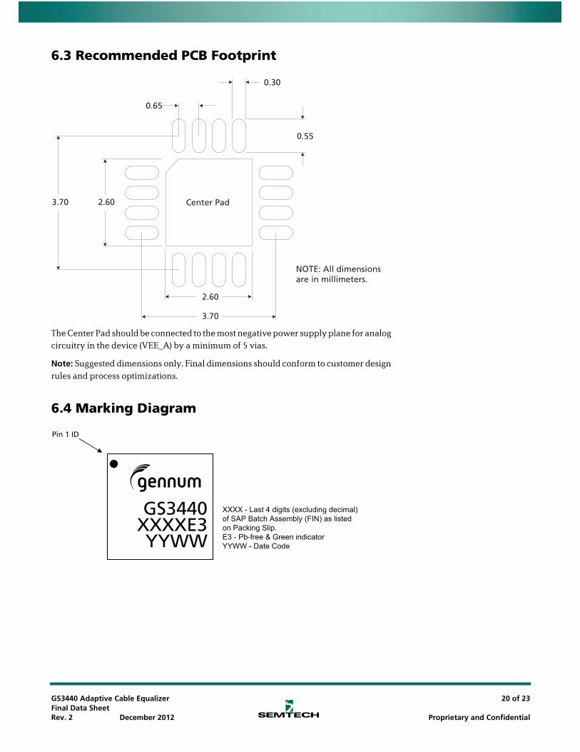
6.3 Recommended PCB Footprint
The Center Pad should be connected to the most negative power supply plane for analog circuitry in the device (VEE_A) by a minimum of 5 vias.
Note: Suggested dimensions only. Final dimensions should conform to customer design rules and process optimizations.
6.4 Marking Diagram
0.30
0.55
2.60
3.70
2.603.70
NOTE: All dimensionsare in millimeters.
0.65
Center Pad
GS3440XXXXE3YYWW
Pin 1 ID
XXXX - Last 4 digits (excluding decimal)of SAP Batch Assembly (FIN) as listedon Packing Slip.E3 - Pb-free & Green indicatorYYWW - Date Code
GS3440 Adaptive Cable EqualizerFinal Data SheetRev. 2 December 2012
21 of 23
Proprietary and Confidential
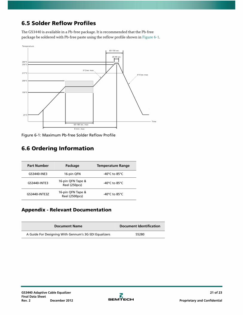
6.5 Solder Reflow ProfilesThe GS3440 is available in a Pb-free package. It is recommended that the Pb-free package be soldered with Pb-free paste using the reflow profile shown in Figure 6-1.
Figure 6-1: Maximum Pb-free Solder Reflow Profile
6.6 Ordering Information
Appendix - Relevant Documentation
25°C
150°C
200°C
217°C
260°C250°C
Time
Temperature
8 min. max
60-180 sec. max
60-150 sec.
20-40 sec.
3°C/sec max
6°C/sec max
Part Number Package Temperature Range
GS3440-INE3 16-pin QFN -40°C to 85°C
GS3440-INTE316-pin QFN Tape &
Reel (250pcs)-40°C to 85°C
GS3440-INTE3Z16-pin QFN Tape &
Reel (2500pcs)-40°C to 85°C
Document Name Document Identification
A Guide For Designing With Gennum’s 3G-SDI Equalizers 55280
GS3440 Adaptive Cable EqualizerFinal Data SheetRev. 2 December 2012
22 of 23
Proprietary and Confidential
Revision History (Document # 56482)
Version ECO PCN Date Changes and/or Modifications
2 010494 – December 2012 Converted document to Final Data Sheet.
1 009989 – November 2012 Updates throughout the document.
0 158278 – June 2012 Converted to Preliminary Data Sheet
H 158055 – May 2012 Updated the description for GAIN_SEL, BYPASS, OP_CTL, SLEEP AND CD in Table 1-1. Included additional row with Input Voltage for Digital pins in Table 2-2.
Change in text throughout document for clarity
G 157993 – May 2012 Modifications throughout the document.
F 157289 – November 2011 Removed the Typical Usages section.
E 157162 – November 2011 Updated the descriptions for the SQ_ADJ and GAIN_SEL pins in Table 1-1 to indicate that they have internal pull-down resistors.
D 156828 – August 2011 Updated power and cable reach numbers in Key Features, Description, DC Electrical Characteristics, AC Electrical Characteristics and Detailed Description.
C 156166 – May 2011 Updated the Power numbers in Table 2-2: DC Electrical Characteristics.
B 156134 – April 2011 Updated the MSL rating in Packaging Data.
A 155973 – April 2011 New document.
© Semtech 2012
All rights reserved. Reproduction in whole or in part is prohibited without the prior written consent of the copyright owner. The information presented in this document does not form part of any quotation or contract, is believed to be accurate and reliable and may be changed without notice. No liability will be accepted by the publisher for any consequence of its use. Publication thereof does not convey nor imply any license under patent or other industrial or intellectual property rights. Semtech assumes no responsibility or liability whatsoever for any failure or unexpected operation resulting from misuse, neglect improper installation, repair or improper handling or unusual physical or electrical stress including, but not limited to, exposure to parameters beyond the specified maximum ratings or operation outside the specified range.
SEMTECH PRODUCTS ARE NOT DESIGNED, INTENDED, AUTHORIZED OR WARRANTED TO BE SUITABLE FOR USE IN LIFE-SUPPORT APPLICATIONS, DEVICES OR SYSTEMS OR OTHER CRITICAL APPLICATIONS. INCLUSION OF SEMTECH PRODUCTS IN SUCH APPLICATIONS IS UNDERSTOOD TO BE UNDERTAKEN SOLELY AT THE CUSTOMER’S OWN RISK. Should a customer purchase or use Semtech products for any such unauthorized application, the customer shall indemnify and hold Semtech and its officers, employees, subsidiaries, affiliates, and distributors harmless against all claims, costs damages and attorney fees which could arise.
Notice: All referenced brands, product names, service names and trademarks are the property of their respective owners.
DOCUMENT IDENTIFICATIONFINAL DATA SHEETInformation relating to this product and the application or design described herein is believed to be reliable, however such information is provided as a guide only and Semtech assumes no liability for any errors in this document, or for the application or design described herein. Semtech reserves the right to make changes to the product or this document at any time without notice.
GS3440 Adaptive Cable EqualizerFinal Data SheetRev. 2 December 2012
23 of 2323
Proprietary and Confidential
Contact Information
Semtech CorporationGennum Products Division
200 Flynn Road, Camarillo, CA 93012Phone: (805) 498-2111, Fax: (805) 498-3804
www.semtech.com
CAUTIONELECTROSTATIC SENSITIVE DEVICES
DO NOT OPEN PACKAGES OR HANDLE EXCEPT AT A STATIC-FREE WORKSTATION
Mouser Electronics
Authorized Distributor
Click to View Pricing, Inventory, Delivery & Lifecycle Information: Semtech:
GS3440-INTE3 GS3440-INTE3Z GS3440-INE3