Embed Size (px)
Citation preview
Automotive Mobile LPDDR2 SDRAMEDB5432BEBH, EDB5432BEPA
Features1
• Ultra low-voltage core and I/O power supplies– VDD2 = 1.14–1.30V– VDDCA/VDDQ = 1.14–1.30V– VDD1 = 1.70–1.95V
• Clock frequency range– 533–10 MHz (data rate range: 1066–20 Mb/s/pin)
• Four-bit prefetch DDR architecture• Four internal banks for concurrent operation• Multiplexed, double data rate, command/address
inputs; commands entered on every CK edge• Bidirectional/differential data strobe per byte of
data (DQS/DQS#)• Programmable READ and WRITE latencies (RL/WL)• Programmable burst lengths: 4, 8, or 16• On-chip temperature sensor to control self refresh
rate• Partial-array self refresh (PASR)2
• Deep power-down mode (DPD)• Selectable output drive strength (DS)• Clock stop capability• RoHS-compliant, “green” packaging
Table 1: Key Timing Parameters
SpeedGrade
Clock Rate(MHz)
Data Rate(Mb/s/pin) RL WL tRCD/tRP
-1D 533 1066 8 4 Typical
Options Marking• VDD2: 1.2V B• Density/Page Size
– 512Mb/2KB - single die 54• Organization
– x32 32• FBGA “green” package
– 134-ball VFBGA(10mm x 11.5mm)
BH
– 168-ball WFBGA(12mm x 12mm)
PA
• Timing – cycle time – 1.875ns @ RL = 8 -1D
• Special options – Standard None– Automotive certified
(Package-level burn-in)A
• Operating temperature range – From –40°C to +85°C IT– From –40°C to +105°C AT– From –40°C to +125°C3 UT
• Revision :E
Notes: 1. All items related to 8-bank in this datasheet are not available. For example per-bank refresh option is not supported.
2. When TC > 105°C, self-refresh mode is notavailable.
3. UT option use based on automotive usagemodel. Please contact Micron sales repre-sentative if you have questions.
512Mb: x32 Automotive Mobile LPDDR2 SDRAMFeatures1
09005aef86573be0u97m_auto_lpddr2_ait_aat_aut.pdf - Rev. H 05/18 EN 1 Micron Technology, Inc. reserves the right to change products or specifications without notice.
© 2015 Micron Technology, Inc. All rights reserved.
Products and specifications discussed herein are subject to change by Micron without notice.
Table 2: Single Channel S4 Configuration Addressing
Architecture 16 Meg x 32
Die configuration 4 Meg x 32 x 4 banks
Row addressing 8K (A[12:0])
Column addressing 512 (A[8:0])
Number of die 1
Die per rank 1
Ranks per channel1 1
Note: 1. A channel is a complete LPDRAM interface, including command/address and data pins.
Figure 1: 512Mb LPDDR2 Part Numbering
E D B 54 32 B E -1D A AT -F
Embedded Memory
TypeD = Packaged device
Product FamilyB = DDR2 Mobile RAM
Density/Page size54 = 512Mb/2KB
Organization32 = x32
Power Supply and InterfaceB = VDD1 = 1.8V; VDD2 = VDDCA = VDDQ = 1.2V;
S4B device; HSUL
Environment Code-F = Lead free (RoHS compliant
and Halogen free)
Operating TemperatureIT = –40°C to +85°C
AT = –40°C to +105°C
UT = –40°C to +125°C
Special OptionsA = Automotive grade
Speed (package only)-1D = 1066 Mbps
PackageBH = 134-ball VFBGA (10mm x 11.5mm)
PA = 168-ball WFBGA (12mm x 12mm)
Revision = E
BH
FBGA Part Marking Decoder
Due to space limitations, FBGA-packaged components have an abbreviated part marking that is different from thepart number. Micron’s FBGA part marking decoder is available at www.micron.com/decoder.
Table 3: Package Codes and Descriptions
PackageCode Ball Count # Ranks # Channels Size (mm)
Die perPackage
Solder BallComposition
BH 134 1 1 10 x 11.5 x 1.0, 0.65 pitch SDP SAC302
PA 168 1 1 12 x 12 x 0.8, 0.5 pitch SDP SAC302
Notes: 1. SDP = Single-die package.2. Solder ball material: SAC302 (96.8% Sn, 3% Ag, 0.2% Cu).
512Mb: x32 Automotive Mobile LPDDR2 SDRAMFeatures1
09005aef86573be0u97m_auto_lpddr2_ait_aat_aut.pdf - Rev. H 05/18 EN 2 Micron Technology, Inc. reserves the right to change products or specifications without notice.
© 2015 Micron Technology, Inc. All rights reserved.
ContentsImportant Notes and Warnings ......................................................................................................................... 9General Description ......................................................................................................................................... 9
General Notes ............................................................................................................................................ 10IDD Specifications ........................................................................................................................................... 11Package Block Diagrams ................................................................................................................................. 14Package Dimensions ....................................................................................................................................... 15Ball Assignments and Descriptions ................................................................................................................. 17Functional Description ................................................................................................................................... 20Power-Up ....................................................................................................................................................... 21
Initialization After RESET (Without Voltage Ramp) ...................................................................................... 23Power-Off ....................................................................................................................................................... 23
Uncontrolled Power-Off .............................................................................................................................. 24Mode Register Definition ................................................................................................................................ 24
Mode Register Assignments and Definitions ................................................................................................ 24ACTIVATE Command ..................................................................................................................................... 35Read and Write Access Modes ......................................................................................................................... 35Burst READ Command ................................................................................................................................... 35
READs Interrupted by a READ ..................................................................................................................... 42Burst WRITE Command .................................................................................................................................. 42
WRITEs Interrupted by a WRITE ................................................................................................................. 45BURST TERMINATE Command ...................................................................................................................... 45Write Data Mask ............................................................................................................................................. 47PRECHARGE Command ................................................................................................................................. 48
READ Burst Followed by PRECHARGE ......................................................................................................... 49WRITE Burst Followed by PRECHARGE ....................................................................................................... 50Auto Precharge ........................................................................................................................................... 51READ Burst with Auto Precharge ................................................................................................................. 51WRITE Burst with Auto Precharge ............................................................................................................... 52
SELF REFRESH Operation ............................................................................................................................... 54Partial-Array Self Refresh – Bank Masking .................................................................................................... 56
MODE REGISTER READ ................................................................................................................................. 57Temperature Sensor ................................................................................................................................... 59DQ Calibration ........................................................................................................................................... 61
MODE REGISTER WRITE Command ............................................................................................................... 63MRW RESET Command .............................................................................................................................. 63MRW ZQ Calibration Commands ................................................................................................................ 64ZQ External Resistor Value, Tolerance, and Capacitive Loading ..................................................................... 66
Power-Down .................................................................................................................................................. 66Deep Power-Down ......................................................................................................................................... 73Input Clock Frequency Changes and Stop Events ............................................................................................. 74
Input Clock Frequency Changes and Clock Stop with CKE LOW ................................................................... 74Input Clock Frequency Changes and Clock Stop with CKE HIGH .................................................................. 75
NO OPERATION Command ............................................................................................................................ 75Simplified Bus Interface State Diagram ........................................................................................................ 75
Truth Tables ................................................................................................................................................... 77Electrical Specifications .................................................................................................................................. 85
Absolute Maximum Ratings ........................................................................................................................ 85Input/Output Capacitance .......................................................................................................................... 85
Electrical Specifications – IDD Specifications and Conditions ............................................................................ 86AC and DC Operating Conditions .................................................................................................................... 89
512Mb: x32 Automotive Mobile LPDDR2 SDRAMFeatures1
09005aef86573be0u97m_auto_lpddr2_ait_aat_aut.pdf - Rev. H 05/18 EN 3 Micron Technology, Inc. reserves the right to change products or specifications without notice.
© 2015 Micron Technology, Inc. All rights reserved.
AC and DC Logic Input Measurement Levels for Single-Ended Signals .............................................................. 91VREF Tolerances .......................................................................................................................................... 92Input Signal ............................................................................................................................................... 93
AC and DC Logic Input Measurement Levels for Differential Signals ................................................................. 95Single-Ended Requirements for Differential Signals ..................................................................................... 96Differential Input Crosspoint Voltage .......................................................................................................... 98Input Slew Rate .......................................................................................................................................... 99
Output Characteristics and Operating Conditions ............................................................................................ 99Single-Ended Output Slew Rate .................................................................................................................. 100Differential Output Slew Rate ..................................................................................................................... 101HSUL_12 Driver Output Timing Reference Load ......................................................................................... 104
Output Driver Impedance .............................................................................................................................. 104Output Driver Impedance Characteristics with ZQ Calibration .................................................................... 105Output Driver Temperature and Voltage Sensitivity ..................................................................................... 106Output Impedance Characteristics Without ZQ Calibration ......................................................................... 106
Clock Specification ........................................................................................................................................ 109tCK(abs), tCH(abs), and tCL(abs) ................................................................................................................ 110
Clock Period Jitter .......................................................................................................................................... 110Clock Period Jitter Effects on Core Timing Parameters ................................................................................. 110Cycle Time Derating for Core Timing Parameters ........................................................................................ 111Clock Cycle Derating for Core Timing Parameters ....................................................................................... 111Clock Jitter Effects on Command/Address Timing Parameters ..................................................................... 111Clock Jitter Effects on READ Timing Parameters .......................................................................................... 111Clock Jitter Effects on WRITE Timing Parameters ........................................................................................ 112
Refresh Requirements .................................................................................................................................... 113AC Timing ..................................................................................................................................................... 114CA and CS# Setup, Hold, and Derating ........................................................................................................... 120Data Setup, Hold, and Slew Rate Derating ....................................................................................................... 127Revision History ............................................................................................................................................ 134
Rev. H – 05/18 ............................................................................................................................................ 134Rev. G – 07/17 ............................................................................................................................................ 134Rev. F – 01/17 ............................................................................................................................................ 134Rev. E – 04/16 ............................................................................................................................................ 134Rev. D – 01/16 ............................................................................................................................................ 134Rev. C – 12/15 ............................................................................................................................................ 134Rev. B – 10/15 ............................................................................................................................................ 134Rev. A – 07/15 ............................................................................................................................................ 134
512Mb: x32 Automotive Mobile LPDDR2 SDRAMFeatures1
09005aef86573be0u97m_auto_lpddr2_ait_aat_aut.pdf - Rev. H 05/18 EN 4 Micron Technology, Inc. reserves the right to change products or specifications without notice.
© 2015 Micron Technology, Inc. All rights reserved.
List of FiguresFigure 1: 512Mb LPDDR2 Part Numbering ....................................................................................................... 2Figure 2: VDD1Typical Self-Refresh Current vs. Temperature ............................................................................ 13Figure 3: VDD2 Typical Self-Refresh Current vs. Temperature ............................................................................ 13Figure 4: Single Rank, Single Channel Package Block Diagram ......................................................................... 14Figure 5: 134-Ball VFBGA – 10mm x 11.5mm (Package Code: BH) .................................................................... 15Figure 6: 168-Ball WFBGA – 12mm x 12mm (Package Code: PA) ....................................................................... 16Figure 7: 134-Ball VFBGA (x32) ...................................................................................................................... 17Figure 8: 168-Ball WFBGA – 12mm x 12mm .................................................................................................... 18Figure 9: Functional Block Diagram ............................................................................................................... 20Figure 10: Voltage Ramp and Initialization Sequence ...................................................................................... 23Figure 11: ACTIVATE Command .................................................................................................................... 35Figure 12: READ Output Timing – tDQSCK (MAX) ........................................................................................... 36Figure 13: READ Output Timing – tDQSCK (MIN) ........................................................................................... 36Figure 14: Burst READ – RL = 5, BL = 4, tDQSCK > tCK ..................................................................................... 37Figure 15: Burst READ – RL = 3, BL = 8, tDQSCK < tCK ..................................................................................... 37Figure 16: tDQSCKDL Timing ........................................................................................................................ 38Figure 17: tDQSCKDM Timing ....................................................................................................................... 39Figure 18: tDQSCKDS Timing ......................................................................................................................... 40Figure 19: Burst READ Followed by Burst WRITE – RL = 3, WL = 1, BL = 4 ......................................................... 41Figure 20: Seamless Burst READ – RL = 3, BL = 4, tCCD = 2 .............................................................................. 41Figure 21: READ Burst Interrupt Example – RL = 3, BL = 8, tCCD = 2 ................................................................. 42Figure 22: Data Input (WRITE) Timing ........................................................................................................... 43Figure 23: Burst WRITE – WL = 1, BL = 4 ......................................................................................................... 43Figure 24: Burst WRITE Followed by Burst READ – RL = 3, WL = 1, BL = 4 ......................................................... 44Figure 25: Seamless Burst WRITE – WL = 1, BL = 4, tCCD = 2 ............................................................................ 44Figure 26: WRITE Burst Interrupt Timing – WL = 1, BL = 8, tCCD = 2 ................................................................ 45Figure 27: Burst WRITE Truncated by BST – WL = 1, BL = 16 ............................................................................ 46Figure 28: Burst READ Truncated by BST – RL = 3, BL = 16 ............................................................................... 47Figure 29: Data Mask Timing ......................................................................................................................... 47Figure 30: Write Data Mask – Second Data Bit Masked .................................................................................... 48Figure 31: READ Burst Followed by PRECHARGE – RL = 3, BL = 8, RU(tRTP(MIN)/tCK) = 2 ................................ 49Figure 32: READ Burst Followed by PRECHARGE – RL = 3, BL = 4, RU(tRTP(MIN)/tCK) = 3 ................................ 50Figure 33: WRITE Burst Followed by PRECHARGE – WL = 1, BL = 4 .................................................................. 51Figure 34: READ Burst with Auto Precharge – RL = 3, BL = 4, RU(tRTP(MIN)/tCK) = 2 ........................................ 52Figure 35: WRITE Burst with Auto Precharge – WL = 1, BL = 4 .......................................................................... 53Figure 36: SELF REFRESH Operation .............................................................................................................. 55Figure 37: MRR Timing – RL = 3, tMRR = 2 ...................................................................................................... 57Figure 38: READ to MRR Timing – RL = 3, tMRR = 2 ......................................................................................... 58Figure 39: Burst WRITE Followed by MRR – RL = 3, WL = 1, BL = 4 ................................................................... 59Figure 40: Temperature Sensor Timing ........................................................................................................... 61Figure 41: MR32 and MR40 DQ Calibration Timing – RL = 3, tMRR = 2 ............................................................. 62Figure 42: MODE REGISTER WRITE Timing – RL = 3, tMRW = 5 ....................................................................... 63Figure 43: ZQ Timings ................................................................................................................................... 65Figure 44: Power-Down Entry and Exit Timing ................................................................................................ 67Figure 45: CKE Intensive Environment ........................................................................................................... 67Figure 46: REFRESH-to-REFRESH Timing in CKE Intensive Environments ...................................................... 67Figure 47: READ to Power-Down Entry ........................................................................................................... 68Figure 48: READ with Auto Precharge to Power-Down Entry ............................................................................ 69Figure 49: WRITE to Power-Down Entry ......................................................................................................... 70Figure 50: WRITE with Auto Precharge to Power-Down Entry .......................................................................... 71
512Mb: x32 Automotive Mobile LPDDR2 SDRAMFeatures1
09005aef86573be0u97m_auto_lpddr2_ait_aat_aut.pdf - Rev. H 05/18 EN 5 Micron Technology, Inc. reserves the right to change products or specifications without notice.
© 2015 Micron Technology, Inc. All rights reserved.
Figure 51: REFRESH Command to Power-Down Entry .................................................................................... 72Figure 52: ACTIVATE Command to Power-Down Entry ................................................................................... 72Figure 53: PRECHARGE Command to Power-Down Entry ............................................................................... 72Figure 54: MRR Command to Power-Down Entry ........................................................................................... 73Figure 55: MRW Command to Power-Down Entry .......................................................................................... 73Figure 56: Deep Power-Down Entry and Exit Timing ....................................................................................... 74Figure 57: Simplified Bus Interface State Diagram ........................................................................................... 76Figure 58: VREF DC Tolerance and VREF AC Noise Limits .................................................................................. 92Figure 59: LPDDR2-466 to LPDDR2-1066 Input Signal .................................................................................... 93Figure 60: LPDDR2-200 to LPDDR2-400 Input Signal ...................................................................................... 94Figure 61: Differential AC Swing Time and tDVAC ........................................................................................... 95Figure 62: Single-Ended Requirements for Differential Signals ........................................................................ 97Figure 63: VIX Definition ................................................................................................................................ 98Figure 64: Differential Input Slew Rate Definition for CK, CK#, DQS, and DQS# ................................................ 99Figure 65: Single-Ended Output Slew Rate Definition ..................................................................................... 100Figure 66: Differential Output Slew Rate Definition ........................................................................................ 102Figure 67: Overshoot and Undershoot Definition ........................................................................................... 103Figure 68: HSUL_12 Driver Output Reference Load for Timing and Slew Rate ................................................. 104Figure 69: Output Driver ............................................................................................................................... 105Figure 70: Output Impedance = 240 Ohms, I-V Curves After ZQRESET ............................................................ 108Figure 71: Output Impedance = 240 Ohms, I-V Curves After Calibration ......................................................... 108Figure 72: Command Input Setup and Hold Timing ....................................................................................... 120Figure 73: Typical Slew Rate and tVAC – tIS for CA and CS# Relative to Clock ................................................... 123Figure 74: Typical Slew Rate – tIH for CA and CS# Relative to Clock ................................................................. 124Figure 75: Tangent Line – tIS for CA and CS# Relative to Clock ........................................................................ 125Figure 76: Tangent Line – tIH for CA and CS# Relative to Clock ....................................................................... 126Figure 77: Typical Slew Rate and tVAC – tDS for DQ Relative to Strobe ............................................................. 130Figure 78: Typical Slew Rate – tDH for DQ Relative to Strobe ........................................................................... 131Figure 79: Tangent Line – tDS for DQ with Respect to Strobe .......................................................................... 132Figure 80: Tangent Line – tDH for DQ with Respect to Strobe .......................................................................... 133
512Mb: x32 Automotive Mobile LPDDR2 SDRAMFeatures1
09005aef86573be0u97m_auto_lpddr2_ait_aat_aut.pdf - Rev. H 05/18 EN 6 Micron Technology, Inc. reserves the right to change products or specifications without notice.
© 2015 Micron Technology, Inc. All rights reserved.
List of TablesTable 1: Key Timing Parameters ....................................................................................................................... 1Table 2: Single Channel S4 Configuration Addressing ........................................................................................ 2Table 3: Package Codes and Descriptions ......................................................................................................... 2Table 4: 16 Meg x 32 IDD Specifications ........................................................................................................... 11Table 5: IDD6 Partial-Array Self Refresh Current ............................................................................................... 12Table 6: Ball/Pad Descriptions ....................................................................................................................... 19Table 7: Initialization Timing Parameters ....................................................................................................... 23Table 8: Power-Off Timing ............................................................................................................................. 24Table 9: Mode Register Assignments .............................................................................................................. 25Table 10: MR0 Device Information (MA[7:0] = 00h) ......................................................................................... 26Table 11: MR0 Op-Code Bit Definitions .......................................................................................................... 26Table 12: MR1 Device Feature 1 (MA[7:0] = 01h) .............................................................................................. 26Table 13: MR1 Op-Code Bit Definitions .......................................................................................................... 27Table 14: Burst Sequence by Burst Length (BL), Burst Type (BT), and Wrap Control (WC) ................................. 27Table 15: No-Wrap Restrictions ...................................................................................................................... 28Table 16: MR2 Device Feature 2 (MA[7:0] = 02h) .............................................................................................. 28Table 17: MR2 Op-Code Bit Definitions .......................................................................................................... 29Table 18: MR3 I/O Configuration 1 (MA[7:0] = 03h) ......................................................................................... 29Table 19: MR3 Op-Code Bit Definitions .......................................................................................................... 29Table 20: MR4 Device Temperature (MA[7:0] = 04h) ........................................................................................ 29Table 21: MR4 Op-Code Bit Definitions .......................................................................................................... 30Table 22: MR5 Basic Configuration 1 (MA[7:0] = 05h) ...................................................................................... 30Table 23: MR5 Op-Code Bit Definitions .......................................................................................................... 30Table 24: MR6 Basic Configuration 2 (MA[7:0] = 06h) ...................................................................................... 31Table 25: MR6 Op-Code Bit Definitions .......................................................................................................... 31Table 26: MR7 Basic Configuration 3 (MA[7:0] = 07h) ...................................................................................... 31Table 27: MR7 Op-Code Bit Definitions .......................................................................................................... 31Table 28: MR8 Basic Configuration 4 (MA[7:0] = 08h) ...................................................................................... 31Table 29: MR8 Op-Code Bit Definitions .......................................................................................................... 31Table 30: MR9 Test Mode (MA[7:0] = 09h) ....................................................................................................... 32Table 31: MR10 Calibration (MA[7:0] = 0Ah) ................................................................................................... 32Table 32: MR10 Op-Code Bit Definitions ........................................................................................................ 32Table 33: MR[11:15] Reserved (MA[7:0] = 0Bh–0Fh) ......................................................................................... 33Table 34: MR16 PASR Bank Mask (MA[7:0] = 010h) .......................................................................................... 33Table 35: MR16 Op-Code Bit Definitions ........................................................................................................ 33Table 36: MR17 PASR Segment Mask (MA[7:0] = 011h) .................................................................................... 33Table 37: Reserved Mode Registers ................................................................................................................. 34Table 38: MR63 RESET (MA[7:0] = 3Fh) – MRW Only ....................................................................................... 34Table 39: Bank Selection for PRECHARGE by Address Bits ............................................................................... 48Table 40: PRECHARGE and Auto Precharge Clarification ................................................................................. 53Table 41: Temperature Sensor Definitions and Operating Conditions .............................................................. 60Table 42: Data Calibration Pattern Description ............................................................................................... 62Table 43: Truth Table for MRR and MRW ........................................................................................................ 63Table 44: Command Truth Table .................................................................................................................... 77Table 45: CKE Truth Table .............................................................................................................................. 78Table 46: Current State Bank n to Command to Bank n Truth Table ................................................................. 79Table 47: Current State Bank n to Command to Bank m Truth Table ................................................................ 81Table 48: DM Truth Table ............................................................................................................................... 84Table 49: Absolute Maximum DC Ratings ....................................................................................................... 85Table 50: Input/Output Capacitance .............................................................................................................. 85
512Mb: x32 Automotive Mobile LPDDR2 SDRAMFeatures1
09005aef86573be0u97m_auto_lpddr2_ait_aat_aut.pdf - Rev. H 05/18 EN 7 Micron Technology, Inc. reserves the right to change products or specifications without notice.
© 2015 Micron Technology, Inc. All rights reserved.
Table 51: Switching for CA Input Signals ......................................................................................................... 86Table 52: Switching for IDD4R .......................................................................................................................... 87Table 53: Switching for IDD4W ......................................................................................................................... 87Table 54: IDD Specification Parameters and Operating Conditions ................................................................... 88Table 55: Recommended DC Operating Conditions ........................................................................................ 89Table 56: Input Leakage Current .................................................................................................................... 90Table 57: Operating Temperature Range ......................................................................................................... 90Table 58: Single-Ended AC and DC Input Levels for CA and CS# Inputs ............................................................ 91Table 59: Single-Ended AC and DC Input Levels for CKE ................................................................................. 91Table 60: Single-Ended AC and DC Input Levels for DQ and DM ...................................................................... 91Table 61: Differential AC and DC Input Levels ................................................................................................. 95Table 62: CK/CK# and DQS/DQS# Time Requirements Before Ringback (tDVAC) ............................................. 96Table 63: Single-Ended Levels for CK, CK#, DQS, DQS# ................................................................................... 97Table 64: Crosspoint Voltage for Differential Input Signals (CK, CK#, DQS, DQS#) ............................................ 98Table 65: Differential Input Slew Rate Definition ............................................................................................. 99Table 66: Single-Ended AC and DC Output Levels ........................................................................................... 99Table 67: Differential AC and DC Output Levels ............................................................................................. 100Table 68: Single-Ended Output Slew Rate Definition ...................................................................................... 100Table 69: Single-Ended Output Slew Rate ...................................................................................................... 100Table 70: Differential Output Slew Rate Definition ......................................................................................... 101Table 71: Differential Output Slew Rate ......................................................................................................... 102Table 72: AC Overshoot/Undershoot Specification ......................................................................................... 102Table 73: Output Driver DC Electrical Characteristics with ZQ Calibration ...................................................... 105Table 74: Output Driver Sensitivity Definition ................................................................................................ 106Table 75: Output Driver Temperature and Voltage Sensitivity ......................................................................... 106Table 76: Output Driver DC Electrical Characteristics Without ZQ Calibration ................................................ 106Table 77: I-V Curves ..................................................................................................................................... 107Table 78: Definitions and Calculations .......................................................................................................... 109Table 79: tCK(abs), tCH(abs), and tCL(abs) Definitions ................................................................................... 110Table 80: Refresh Requirement Parameters (Per Density) ............................................................................... 113Table 81: AC Timing ..................................................................................................................................... 114Table 82: CA and CS# Setup and Hold Base Values (>400 MHz, 1 V/ns Slew Rate) ............................................ 121Table 83: CA and CS# Setup and Hold Base Values (<400 MHz, 1 V/ns Slew Rate) ............................................ 121Table 84: Derating Values for AC/DC-Based tIS/tIH (AC220) ........................................................................... 122Table 85: Derating Values for AC/DC-Based tIS/tIH (AC300) ........................................................................... 122Table 86: Required Time for Valid Transition – tVAC > VIH(AC) and < VIL(AC) ....................................................... 122Table 87: Data Setup and Hold Base Values (>400 MHz, 1 V/ns Slew Rate) ....................................................... 127Table 88: Data Setup and Hold Base Values (<400 MHz, 1 V/ns Slew Rate) ....................................................... 128Table 89: Derating Values for AC/DC-Based tDS/tDH (AC220) ........................................................................ 128Table 90: Derating Values for AC/DC-Based tDS/tDH (AC300) ........................................................................ 129Table 91: Required Time for Valid Transition – tVAC > VIH(AC) or < VIL(AC) ......................................................... 129
512Mb: x32 Automotive Mobile LPDDR2 SDRAMFeatures1
09005aef86573be0u97m_auto_lpddr2_ait_aat_aut.pdf - Rev. H 05/18 EN 8 Micron Technology, Inc. reserves the right to change products or specifications without notice.
© 2015 Micron Technology, Inc. All rights reserved.
Important Notes and WarningsMicron Technology, Inc. ("Micron") reserves the right to make changes to information published in this document,including without limitation specifications and product descriptions. This document supersedes and replaces allinformation supplied prior to the publication hereof. You may not rely on any information set forth in this docu-ment if you obtain the product described herein from any unauthorized distributor or other source not authorizedby Micron.
Automotive Applications. Products are not designed or intended for use in automotive applications unless specifi-cally designated by Micron as automotive-grade by their respective data sheets. Distributor and customer/distrib-utor shall assume the sole risk and liability for and shall indemnify and hold Micron harmless against all claims,costs, damages, and expenses and reasonable attorneys' fees arising out of, directly or indirectly, any claim ofproduct liability, personal injury, death, or property damage resulting directly or indirectly from any use of non-automotive-grade products in automotive applications. Customer/distributor shall ensure that the terms and con-ditions of sale between customer/distributor and any customer of distributor/customer (1) state that Micronproducts are not designed or intended for use in automotive applications unless specifically designated by Micronas automotive-grade by their respective data sheets and (2) require such customer of distributor/customer to in-demnify and hold Micron harmless against all claims, costs, damages, and expenses and reasonable attorneys'fees arising out of, directly or indirectly, any claim of product liability, personal injury, death, or property damageresulting from any use of non-automotive-grade products in automotive applications.
Critical Applications. Products are not authorized for use in applications in which failure of the Micron compo-nent could result, directly or indirectly in death, personal injury, or severe property or environmental damage("Critical Applications"). Customer must protect against death, personal injury, and severe property and environ-mental damage by incorporating safety design measures into customer's applications to ensure that failure of theMicron component will not result in such harms. Should customer or distributor purchase, use, or sell any Microncomponent for any critical application, customer and distributor shall indemnify and hold harmless Micron andits subsidiaries, subcontractors, and affiliates and the directors, officers, and employees of each against all claims,costs, damages, and expenses and reasonable attorneys' fees arising out of, directly or indirectly, any claim ofproduct liability, personal injury, or death arising in any way out of such critical application, whether or not Mi-cron or its subsidiaries, subcontractors, or affiliates were negligent in the design, manufacture, or warning of theMicron product.
Customer Responsibility. Customers are responsible for the design, manufacture, and operation of their systems,applications, and products using Micron products. ALL SEMICONDUCTOR PRODUCTS HAVE INHERENT FAIL-URE RATES AND LIMITED USEFUL LIVES. IT IS THE CUSTOMER'S SOLE RESPONSIBILITY TO DETERMINEWHETHER THE MICRON PRODUCT IS SUITABLE AND FIT FOR THE CUSTOMER'S SYSTEM, APPLICATION, ORPRODUCT. Customers must ensure that adequate design, manufacturing, and operating safeguards are includedin customer's applications and products to eliminate the risk that personal injury, death, or severe property or en-vironmental damages will result from failure of any semiconductor component.
Limited Warranty. In no event shall Micron be liable for any indirect, incidental, punitive, special or consequentialdamages (including without limitation lost profits, lost savings, business interruption, costs related to the removalor replacement of any products or rework charges) whether or not such damages are based on tort, warranty,breach of contract or other legal theory, unless explicitly stated in a written agreement executed by Micron's dulyauthorized representative.
General DescriptionThe 512Mb Mobile Low-Power DDR2 SDRAM (LPDDR2) is a high-speed CMOS, dynam-ic random-access memory containing 536,870,912 bits. The LPDDR2-S4 device is inter-nally configured as an four-bank DRAM. Each of the x32’s 134,217,728-bit banks is or-ganized as 8192 rows by 512 columns by 32 bits.
512Mb: x32 Automotive Mobile LPDDR2 SDRAMImportant Notes and Warnings
09005aef86573be0u97m_auto_lpddr2_ait_aat_aut.pdf - Rev. H 05/18 EN 9 Micron Technology, Inc. reserves the right to change products or specifications without notice.
© 2015 Micron Technology, Inc. All rights reserved.
General Notes
Throughout the data sheet, figures and text refer to DQs as “DQ.” DQ should be inter-preted as any or all DQ collectively, unless specifically stated otherwise.
“DQS” and “CK” should be interpreted as DQS, DQS# and CK, CK# respectively, unlessspecifically stated otherwise. “BA” includes all BA pins used for a given density.
In timing diagrams, “CMD” is used as an indicator only. Actual signals occur on CA[9:0].
VREF indicates VREFCA and VREFDQ.
Complete functionality may be described throughout the entire document. Any page ordiagram may have been simplified to convey a topic and may not be inclusive of all re-quirements.
Any specific requirement takes precedence over a general statement.
Any functionality not specifically stated herein is considered undefined, illegal, is notsupported, and will result in unknown operation.
512Mb: x32 Automotive Mobile LPDDR2 SDRAMGeneral Description
09005aef86573be0u97m_auto_lpddr2_ait_aat_aut.pdf - Rev. H 05/18 EN 10 Micron Technology, Inc. reserves the right to change products or specifications without notice.
© 2015 Micron Technology, Inc. All rights reserved.
IDD Specifications
Table 4: 16 Meg x 32 IDD Specifications
VDD2, VDDQ, VDDCA = 1.14–1.30V; VDD1 = 1.70–1.95V
Parameter SupplySpeed Grade
Unit-1D
IDD01 VDD1 6 mA
IDD02 VDD2 30
IDD0,in VDDCA + VDDQ 1
IDD2P1 VDD1 0.6 mA
IDD2P2 VDD2 1.6
IDD2P,in VDDCA + VDDQ 0.1
IDD2PS1 VDD1 0.6 mA
IDD2PS2 VDD2 1.6
IDD2PS,in VDDCA + VDDQ 0.1
IDD2N1 VDD1 0.6 mA
IDD2N2 VDD2 20
IDD2N,in VDDCA + VDDQ 1
IDD2NS1 VDD1 0.6 mA
IDD2NS2 VDD2 12
IDD2NS,in VDDCA + VDDQ 1
IDD3P1 VDD1 1.4 mA
IDD3P2 VDD2 5
IDD3P,in VDDCA + VDDQ 0.1
IDD3PS1 VDD1 1.4 mA
IDD3PS2 VDD2 5
IDD3PS,in VDDCA + VDDQ 0.1
IDD3N1 VDD1 1.5 mA
IDD3N2 VDD2 22
IDD3N,in VDDCA + VDDQ 1
IDD3NS1 VDD1 1.5 mA
IDD3NS2 VDD2 14
IDD3NS,in VDDCA + VDDQ 1
IDD4R1 VDD1 2 mA
IDD4R2 VDD2 180
IDD4R,in VDDCA 2
IDD4W1 VDD1 2 mA
IDD4W2 VDD2 200
IDD4W,in VDDCA + VDDQ 1
512Mb: x32 Automotive Mobile LPDDR2 SDRAMIDD Specifications
09005aef86573be0u97m_auto_lpddr2_ait_aat_aut.pdf - Rev. H 05/18 EN 11 Micron Technology, Inc. reserves the right to change products or specifications without notice.
© 2015 Micron Technology, Inc. All rights reserved.
Table 4: 16 Meg x 32 IDD Specifications (Continued)
VDD2, VDDQ, VDDCA = 1.14–1.30V; VDD1 = 1.70–1.95V
Parameter SupplySpeed Grade
Unit-1D
IDD51 VDD1 20 mA
IDD52 VDD2 70
IDD5,in VDDCA + VDDQ 1
IDD5AB1 VDD1 2 mA
IDD5AB2 VDD2 23
IDD5AB,in VDDCA + VDDQ 1
IDD61 VDD1 – See Table 5
IDD62 VDD2 –
IDD6,in VDDCA + VDDQ –
IDD81 VDD1 0.05 mA
IDD82 VDD2 0.05
IDD8,in VDDCA + VDDQ 0.02
Table 5: IDD6 Partial-Array Self Refresh Current
VDD2, VDDQ, VDDCA = 1.14–1.30V; VDD1 = 1.70–1.95VPASR Supply Value (-40˚C to +85˚C) Value (+85˚C to +105˚C) Value (+105˚C to +125˚C) Unit
Full array VDD1 230 2100 – μA
VDD2 700 4400 –
VDDi 20 20 –
1/2 array VDD1 200 2000 –
VDD2 500 2900 –
VDDi 20 20 –
1/4 array VDD1 190 1800 –
VDD2 400 2000 –
VDDi 20 20 –
1/8 array VDD1 185 1700 –
VDD2 360 1800 –
VDDi 20 20 –
Notes: 1. LPDDR2-S4 SDRAM devices support both bank-masking and segment-masking. IDD6 PASRcurrents are measured using bank-masking only.
2. When TC > 105°C: self-refresh mode is not available.
512Mb: x32 Automotive Mobile LPDDR2 SDRAMIDD Specifications
09005aef86573be0u97m_auto_lpddr2_ait_aat_aut.pdf - Rev. H 05/18 EN 12 Micron Technology, Inc. reserves the right to change products or specifications without notice.
© 2015 Micron Technology, Inc. All rights reserved.
Figure 2: VDD1Typical Self-Refresh Current vs. Temperature
0.8
0.7
0.6
0.5
0.4
0.3
0.2
0.1
0.0–50 0 50 100 150
I DD
6 (m
A)
Temperature (°C)
Figure 3: VDD2 Typical Self-Refresh Current vs. Temperature
4.0
3.5
3.0
2.5
2.0
1.5
1.0
0.5
0.0–50 0 50 100 150
I DD
6 (m
A)
Temperature (°C)
512Mb: x32 Automotive Mobile LPDDR2 SDRAMIDD Specifications
09005aef86573be0u97m_auto_lpddr2_ait_aat_aut.pdf - Rev. H 05/18 EN 13 Micron Technology, Inc. reserves the right to change products or specifications without notice.
© 2015 Micron Technology, Inc. All rights reserved.
Package Block Diagrams
Figure 4: Single Rank, Single Channel Package Block Diagram
LPDDR2
Die 0
CS0#
CKE0
CK
CK#
DM
CA[9:0]
DQ, DQS
ZQ
RZQ
VDD1 VDD2 VDDQ VDDCA VSS
VREFDQVREFCA
512Mb: x32 Automotive Mobile LPDDR2 SDRAMPackage Block Diagrams
09005aef86573be0u97m_auto_lpddr2_ait_aat_aut.pdf - Rev. H 05/18 EN 14 Micron Technology, Inc. reserves the right to change products or specifications without notice.
© 2015 Micron Technology, Inc. All rights reserved.
Package Dimensions
Figure 5: 134-Ball VFBGA – 10mm x 11.5mm (Package Code: BH)
Seating plane
0.08 A
Ball A1 ID(covered by SR)
11.5 ±0.1
10 ±0.1
10.4 CTR
5.85 CTR
Ball A1 ID
0.9 ±0.1
0.22 MIN
134X Ø0.36Dimensionsapply to solderballs post-reflowon Ø0.30 SMDball pads.
0.65 TYP0.65 TYP
ABCDEFGHJKLMNPRTU
12345678910
A
Note: 1. All dimensions are in millimeters.
512Mb: x32 Automotive Mobile LPDDR2 SDRAMPackage Dimensions
09005aef86573be0u97m_auto_lpddr2_ait_aat_aut.pdf - Rev. H 05/18 EN 15 Micron Technology, Inc. reserves the right to change products or specifications without notice.
© 2015 Micron Technology, Inc. All rights reserved.
Figure 6: 168-Ball WFBGA – 12mm x 12mm (Package Code: PA)
Seating plane
0.08 A
Ball A1 ID
0.24 MIN
0.7 ±0.1
11 CTR
12 ±0.1
0.5 TYP
11 CTR
12 ±0.1
0.5 TYP
Ball A1 ID
168X Ø0.355Dimensionsapply to solderballs post-reflowon Ø0.28 SMDball pads.
ABCDEFGHJKLMNPRTUVWYAAABAC
23 21 19 17 15 13 11 9 7 5 3 122 20 18 16 14 12 10 8 6 4 2
A
Note: 1. All dimensions are in millimeters.
512Mb: x32 Automotive Mobile LPDDR2 SDRAMPackage Dimensions
09005aef86573be0u97m_auto_lpddr2_ait_aat_aut.pdf - Rev. H 05/18 EN 16 Micron Technology, Inc. reserves the right to change products or specifications without notice.
© 2015 Micron Technology, Inc. All rights reserved.
Ball Assignments and Descriptions
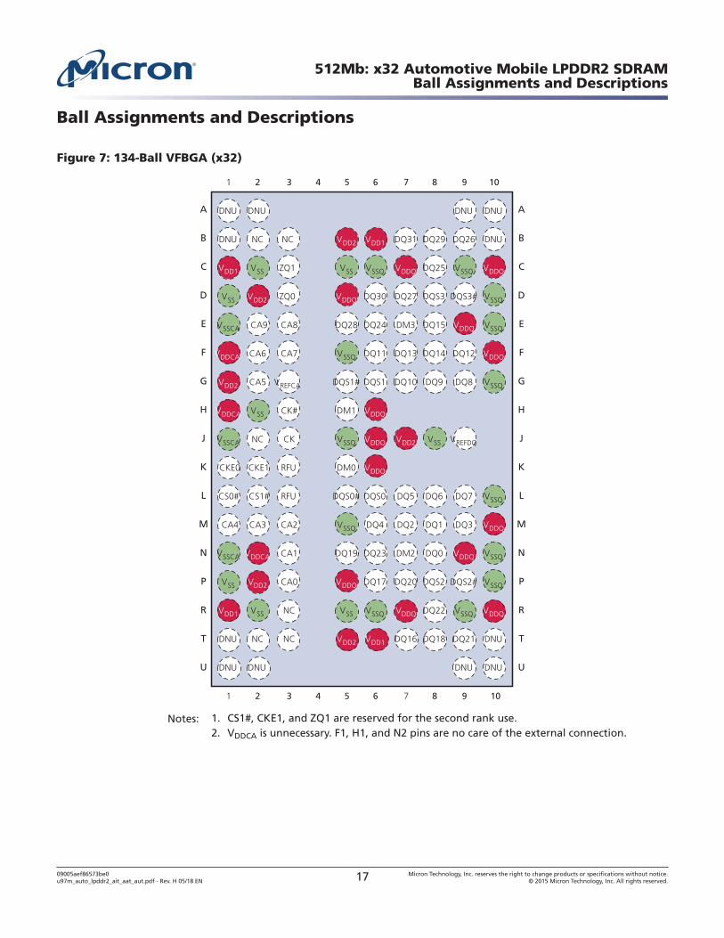
Figure 7: 134-Ball VFBGA (x32)
A
B
C
D
E
F
G
H
J
K
L
M
N
P
R
T
U
A
B
C
D
E
F
G
H
J
K
L
M
N
P
R
T
U
1
DNU
DNU
VDD1
VSS
VSSCA
VDDCA
VDD2
VDDCA
VSSCA
CKE0
CS0#
CA4
VSSCA
VSS
VDD1
DNU
DNU
1
2
DNU
NC
VSS
VDD2
CA9
CA6
CA5
VSS
NC
CKE1
CS1#
CA3
VDDCA
VDD2
VSS
NC
DNU
2
4
4
3
NC
ZQ1
ZQ0
CA8
CA7
VREFCA
CK#
CK
RFU
RFU
CA2
CA1
CA0
NC
NC
3
5
VDD2
VSS
VDDQ
DQ28
VSSQ
DQS1#
DM1
VSSQ
DM0
DQS0#
VSSQ
DQ19
VDDQ
VSS
VDD2
5
6
VDD1
VSSQ
DQ30
DQ24
DQ11
DQS1
VDDQ
VDDQ
VDDQ
DQS0
DQ4
DQ23
DQ17
VSSQ
VDD1
6
7
DQ31
VDDQ
DQ27
DM3
DQ13
DQ10
VDD2
DQ5
DQ2
DM2
DQ20
VDDQ
DQ16
7
8
DQ29
DQ25
DQS3
DQ15
DQ14
DQ9
VSS
DQ6
DQ1
DQ0
DQS2
DQ22
DQ18
8
9
DNU
DQ26
VSSQ
DQS3#
VDDQ
DQ12
DQ8
VREFDQ
DQ7
DQ3
VDDQ
DQS2#
VSSQ
DQ21
DNU
9
10
DNU
DNU
VDDQ
VSSQ
VSSQ
VDDQ
VSSQ
VSSQ
VDDQ
VSSQ
VSSQ
VDDQ
DNU
DNU
10
Notes: 1. CS1#, CKE1, and ZQ1 are reserved for the second rank use.2. VDDCA is unnecessary. F1, H1, and N2 pins are no care of the external connection.
512Mb: x32 Automotive Mobile LPDDR2 SDRAMBall Assignments and Descriptions
09005aef86573be0u97m_auto_lpddr2_ait_aat_aut.pdf - Rev. H 05/18 EN 17 Micron Technology, Inc. reserves the right to change products or specifications without notice.
© 2015 Micron Technology, Inc. All rights reserved.
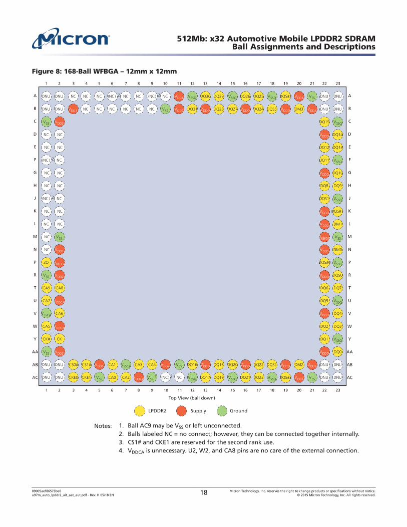
Figure 8: 168-Ball WFBGA – 12mm x 12mm
A
B
C
D
E
F
G
H
J
K
L
M
N
P
R
T
U
V
W
Y
AA
AB
AC
A
B
C
D
E
F
G
H
J
K
L
M
N
P
R
T
U
V
W
Y
AA
AB
AC
Top View (ball down)
1
DNU
DNU
VSS
NC
NC
(NC) 2
NC
NC
(NC) 2
NC
NC
NC
NC
ZQ
VSS
CA9
CA7
VSSCA
CA5
CK#
VSS
DNU
DNU
1
2
DNU
DNU
VDD2
NC
NC
NC
NC
NC
NC
NC
NC
VSS
VDD1
VREFCA
VDD2
CA8
VDDCA
CA6
VDDCA
CK
VDD2
DNU
DNU
2
4
NC
NC
CS1#
CKE1
4
3
NC
VDD1
CS0#
CKE0
3
5
NC
NC
VDD1
VSS
5
6
(NC) 2
NC
CA1
CA0
6
7
NC
NC
VSSCA
CA2
7
8
NC
NC
CA3
VDDCA
8
9
(NC) 2
NC
CA4
VSS 1
9
11
VDD1
VDD2
VSS
NC
11
13
DQ30
VDDQ
VDDQ
DQ17
13
14
DQ29
DQ28
DQ18
DQ19
14
15
VSSQ
DQ27
DQ20
VSSQ
15
16
DQ26
VDDQ
VDDQ
DQ21
16
22
DNU
DNU
DQ15
VDDQ
DQ12
DQ11
VDDQ
DQ8
DQS1
VDDQ
VDD2
VREFDQ
VDD1
DQS#0
VDDQ
DQ6
DQ5
VDDQ
DQ2
DQ1
VDDQ
DNU
DNU
22
23
DNU
DNU
VSSQ
DQ14
DQ13
VSSQ
DQ10
DQ9
VSSQ
DQS#1
DM1
VSS
DM0
VSSQ
DQS0
DQ7
VSSQ
DQ4
DQ3
VSSQ
DQ0
DNU
DNU
23
10
NC
VSS
VDD2
(NC) 2
10
12
VSSQ
DQ31
DQ16
VSSQ
12
18
VSSQ
DQS3
DQS2
VSSQ
18
19
DQS#3
VDDQ
VDDQ
DQS#2
19
20
VDD1
DM3
DM2
VDD1
20
21
VSS
VDD2
VDD2
VSS
21
17
DQ25
DQ24
DQ22
DQ23
17
Supply GroundLPDDR2
Notes: 1. Ball AC9 may be VSS or left unconnected.2. Balls labeled NC = no connect; however, they can be connected together internally.3. CS1# and CKE1 are reserved for the second rank use.4. VDDCA is unnecessary. U2, W2, and CA8 pins are no care of the external connection.
512Mb: x32 Automotive Mobile LPDDR2 SDRAMBall Assignments and Descriptions
09005aef86573be0u97m_auto_lpddr2_ait_aat_aut.pdf - Rev. H 05/18 EN 18 Micron Technology, Inc. reserves the right to change products or specifications without notice.
© 2015 Micron Technology, Inc. All rights reserved.
Table 6: Ball/Pad Descriptions
Symbol Type Description
CA[9:0] Input Command/address inputs: Provide the command and address inputs accordingto the command truth table.
CK, CK# Input Clock: CK and CK# are differential clock inputs. All CA inputs are sampled onboth rising and falling edges of CK. CS and CKE inputs are sampled at the risingedge of CK. AC timings are referenced to clock.
CKE[1:0] Input Clock enable: CKE HIGH activates and CKE LOW deactivates the internal clocksignals, input buffers, and output drivers. Power-saving modes are entered andexited via CKE transitions. CKE is considered part of the command code. CKE issampled at the rising edge of CK.
CS[1:0]# Input Chip select: CS# is considered part of the command code and is sampled at therising edge of CK.
DM[3:0] Input Input data mask: DM is an input mask signal for write data. Although DM ballsare input-only, the DM loading is designed to match that of DQ and DQS balls.DM[3:0] is DM for each of the four data bytes, respectively.
DQ[31:0] I/O Data input/output: Bidirectional data bus.
DQS[3:0],DQS[3:0]#
I/O Data strobe: The data strobe is bidirectional (used for read and write data) andcomplementary (DQS and DQS#). It is edge-aligned output with read data andcentered input with write data. DQS[3:0]/DQS[3:0]# is DQS for each of the fourdata bytes, respectively.
VDDQ Supply DQ power supply: Isolated on the die for improved noise immunity.
VSSQ Supply DQ ground: Isolated on the die for improved noise immunity.
VDDCA Supply Command/address power supply: Command/address power supply.
VSSCA Supply Command/address ground: Isolated on the die for improved noise immunity.
VDD1 Supply Core power: Supply 1.
VDD2 Supply Core power: Supply 2.
VSS Supply Common ground
VREFCA, VREFDQ Supply Reference voltage: VREFCA is reference for command/address input buffers,VREFDQ is reference for DQ input buffers.
ZQ Reference External impedance (240 ohm): This signal is used to calibrate the device out-put impedance.
DNU – Do not use: Must be grounded or left floating.
NC – No connect: Not internally connected.
(NC) – No connect: Balls indicated as (NC) are no connects, however, they could be con-nected together internally.
Note: 1. CS1# and CKE1 are reserved for the second rank use.
512Mb: x32 Automotive Mobile LPDDR2 SDRAMBall Assignments and Descriptions
09005aef86573be0u97m_auto_lpddr2_ait_aat_aut.pdf - Rev. H 05/18 EN 19 Micron Technology, Inc. reserves the right to change products or specifications without notice.
© 2015 Micron Technology, Inc. All rights reserved.
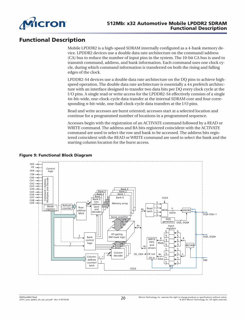
Functional DescriptionMobile LPDDR2 is a high-speed SDRAM internally configured as a 4-bank memory de-vice. LPDDR2 devices use a double data rate architecture on the command/address(CA) bus to reduce the number of input pins in the system. The 10-bit CA bus is used totransmit command, address, and bank information. Each command uses one clock cy-cle, during which command information is transferred on both the rising and fallingedges of the clock.
LPDDR2-S4 devices use a double data rate architecture on the DQ pins to achieve high-speed operation. The double data rate architecture is essentially a 4n prefetch architec-ture with an interface designed to transfer two data bits per DQ every clock cycle at theI/O pins. A single read or write access for the LPDDR2-S4 effectively consists of a single4n-bit-wide, one-clock-cycle data transfer at the internal SDRAM core and four corre-sponding n-bit-wide, one-half-clock-cycle data transfers at the I/O pins.
Read and write accesses are burst oriented; accesses start at a selected location andcontinue for a programmed number of locations in a programmed sequence.
Accesses begin with the registration of an ACTIVATE command followed by a READ orWRITE command. The address and BA bits registered coincident with the ACTIVATEcommand are used to select the row and bank to be accessed. The address bits regis-tered coincident with the READ or WRITE command are used to select the bank and thestarting column location for the burst access.
Figure 9: Functional Block Diagram
x Row-address
MUX
Controllogic
Column-addresscounter/
latch
Moderegisters
Columndecoder
Bank 0
Memory array
Bank 0row-
addresslatchand
decoder
Sense amplifier
Bankcontrollogic
Bank 1Bank 2
Bank 3
x
y - 1
2
2
Refreshcounter
n
nn
4n
4n
4n
CK out
DATA
DQS, DQS#
CK, CK#
COL0
COL0
CK in
MUX
DQSgenerator
n
n
n
n
n
DQS, DQS#
Readlatch
WRITEFIFOand
drivers
Data
n
n
n
n4n
4
4
4
4Mask
4
4
4
448
n
n
1
Bank 1Bank 2
Bank 3
Inputregisters
DM
DQ0–DQn-1
CA0CA1
CK
CS#
CA2
CK#
Co
mm
and
/ A
dd
ress
Mu
ltip
lex
and
Dec
od
e
CKE
CA3CA4CA5CA6CA7CA8CA9
I/O gatingDM mask logic
DRVRS
RCVRS
512Mb: x32 Automotive Mobile LPDDR2 SDRAMFunctional Description
09005aef86573be0u97m_auto_lpddr2_ait_aat_aut.pdf - Rev. H 05/18 EN 20 Micron Technology, Inc. reserves the right to change products or specifications without notice.
© 2015 Micron Technology, Inc. All rights reserved.
Power-UpThe following sequence must be used to power up the device. Unless specified other-wise, this procedure is mandatory (see Figure 10 (page 23)). Power-up and initializa-tion by means other than those specified will result in undefined operation.
1. Voltage Ramp
While applying power (after Ta), CKE must be held LOW ( 0.2 × VDDCA), and all otherinputs must be between VILmin and VIHmax. The device outputs remain at High-Z whileCKE is held LOW.
On or before the completion of the voltage ramp (Tb), CKE must be held LOW. DQ, DM,DQS, and DQS# voltage levels must be between VSSQ and VDDQ during voltage ramp toavoid latchup. CK, CK#, CS#, and CA input levels must be between VSSCA and VDDCA dur-ing voltage ramp to avoid latchup.
The following conditions apply for voltage ramp:
• Ta is the point when any power supply first reaches 300mV.• Noted conditions apply between Ta and power-down (controlled or uncontrolled).• Tb is the point at which all supply and reference voltages are within their defined op-
erating ranges.• Power ramp duration tINIT0 (Tb - Ta) must not exceed 20ms.• For supply and reference voltage operating conditions, see the Recommended DC
Operating Conditions table.• The voltage difference between any of VSS, VSSQ, and VSSCA pins must not exceed
100mV.
Voltage Ramp Completion
After Ta is reached:
• VDD1 must be greater than VDD2 - 200mV• VDD1 and VDD2 must be greater than VDDCA - 200mV• VDD1 and VDD2 must be greater than VDDQ - 200mV• VREF must always be less than all other supply voltages
Beginning at Tb, CKE must remain LOW for at least tINIT1 = 100ns, after which CKE canbe asserted HIGH. The clock must be stable at least tINIT2 = 5 × tCK prior to the firstCKE LOW-to-HIGH transition (Tc). CKE, CS#, and CA inputs must observe setup andhold requirements (tIS, tIH) with respect to the first rising clock edge (and to subse-quent falling and rising edges).
If any MRRs are issued, the clock period must be within the range defined for tCKb(18ns to 100ns). MRWs can be issued at normal clock frequencies as long as all AC tim-ings are met. Some AC parameters (for example, tDQSCK) could have relaxed timings(such as tDQSCKb) before the system is appropriately configured. While keeping CKEHIGH, NOP commands must be issued for at least tINIT3 = 200μs (Td).
2. RESET Command
After tINIT3 is satisfied, the MRW RESET command must be issued (Td). An optionalPRECHARGE ALL command can be issued prior to the MRW RESET command.
Wait at least tINIT4 while keeping CKE asserted and issuing NOP commands.
512Mb: x32 Automotive Mobile LPDDR2 SDRAMPower-Up
09005aef86573be0u97m_auto_lpddr2_ait_aat_aut.pdf - Rev. H 05/18 EN 21 Micron Technology, Inc. reserves the right to change products or specifications without notice.
© 2015 Micron Technology, Inc. All rights reserved.
3. MRRs and Device Auto Initialization (DAI) Polling
After tINIT4 is satisfied (Te), only MRR commands and power-down entry/exit com-mands are supported. After Te, CKE can go LOW in alignment with power-down entryand exit specifications (see Power-Down).
The MRR command can be used to poll the DAI bit, which indicates when device autoinitialization is complete; otherwise, the controller must wait a minimum of tINIT5, oruntil the DAI bit is set, before proceeding.
Because the memory output buffers are not properly configured by Te, some AC param-eters must use relaxed timing specifications before the system is appropriately config-ured.
After the DAI bit (MR0, DAI) is set to zero by the memory device (DAI complete), thedevice is in the idle state (Tf). DAI status can be determined by issuing the MRR com-mand to MR0.
The device sets the DAI bit no later than tINIT5 after the RESET command. The control-ler must wait at least tINIT5 or until the DAI bit is set before proceeding.
4. ZQ Calibration
After tINIT5 (Tf), the MRW initialization calibration (ZQ calibration) command can beissued to the memory (MR10).
This command is used to calibrate output impedance over process, voltage, and tem-perature. In systems where more than one Mobile LPDDR2 device exists on the samebus, the controller must not overlap MRW ZQ calibration commands. The device isready for normal operation after tZQINIT.
5. Normal Operation
After (Tg), MRW commands must be used to properly configure the memory (outputbuffer drive strength, latencies, etc.). Specifically, MR1, MR2, and MR3 must be set toconfigure the memory for the target frequency and memory configuration.
After the initialization sequence is complete, the device is ready for any valid command.After Tg, the clock frequency can be changed using the procedure described in InputClock Frequency Changes and Clock Stop with CKE HIGH (page 75).
512Mb: x32 Automotive Mobile LPDDR2 SDRAMPower-Up
09005aef86573be0u97m_auto_lpddr2_ait_aat_aut.pdf - Rev. H 05/18 EN 22 Micron Technology, Inc. reserves the right to change products or specifications without notice.
© 2015 Micron Technology, Inc. All rights reserved.
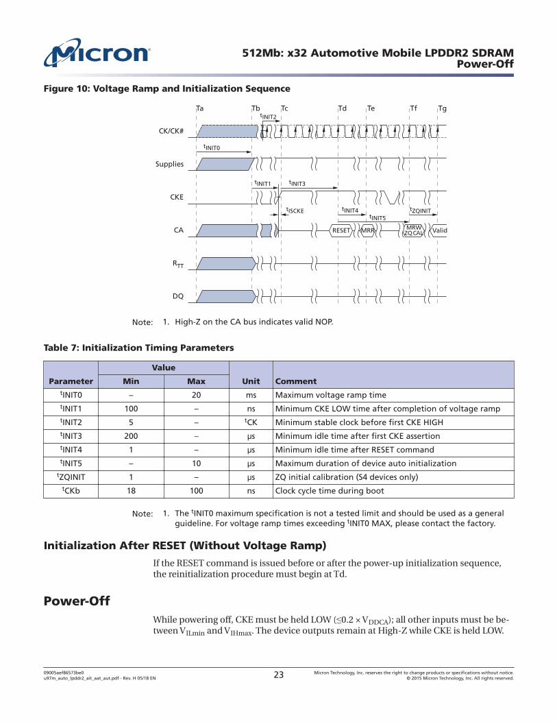
Figure 10: Voltage Ramp and Initialization Sequence
Ta Tb Tc Td Te Tf Tg
RESET MRR MRWZQ_CAL Valid
CK/CK#
Supplies
CKE
CA
RTT
DQ
tINIT0
tINIT1 tINIT3
tINIT4 tZQINITtINIT5
tISCKE
tINIT2
Note: 1. High-Z on the CA bus indicates valid NOP.
Table 7: Initialization Timing Parameters
Parameter
Value
Unit CommentMin MaxtINIT0 – 20 ms Maximum voltage ramp timetINIT1 100 – ns Minimum CKE LOW time after completion of voltage ramptINIT2 5 – tCK Minimum stable clock before first CKE HIGHtINIT3 200 – μs Minimum idle time after first CKE assertiontINIT4 1 – μs Minimum idle time after RESET commandtINIT5 – 10 μs Maximum duration of device auto initialization
tZQINIT 1 – μs ZQ initial calibration (S4 devices only)tCKb 18 100 ns Clock cycle time during boot
Note: 1. The tINIT0 maximum specification is not a tested limit and should be used as a generalguideline. For voltage ramp times exceeding tINIT0 MAX, please contact the factory.
Initialization After RESET (Without Voltage Ramp)
If the RESET command is issued before or after the power-up initialization sequence,the reinitialization procedure must begin at Td.
Power-OffWhile powering off, CKE must be held LOW ( 0.2 × VDDCA); all other inputs must be be-tween VILmin and VIHmax. The device outputs remain at High-Z while CKE is held LOW.
512Mb: x32 Automotive Mobile LPDDR2 SDRAMPower-Off
09005aef86573be0u97m_auto_lpddr2_ait_aat_aut.pdf - Rev. H 05/18 EN 23 Micron Technology, Inc. reserves the right to change products or specifications without notice.
© 2015 Micron Technology, Inc. All rights reserved.
DQ, DM, DQS, and DQS# voltage levels must be between VSSQ and VDDQ during thepower-off sequence to avoid latchup. CK, CK#, CS#, and CA input levels must be be-tween VSSCA and VDDCA during the power-off sequence to avoid latchup.
Tx is the point where any power supply drops below the minimum value specified inthe Recommended DC Operating Conditions table.
Tz is the point where all power supplies are below 300mV. After Tz, the device is pow-ered off.
Required Power Supply Conditions Between Tx and Tz:
• VDD1 must be greater than VDD2 - 200mV• VDD1 must be greater than VDDCA - 200mV• VDD1 must be greater than VDDQ - 200mV• VREF must always be less than all other supply voltages
The voltage difference between VSS, VSSQ, and VSSCA must not exceed 100mV.
For supply and reference voltage operating conditions, see Recommended DC Operat-ing Conditions table.
Uncontrolled Power-Off
When an uncontrolled power-off occurs, the following conditions must be met:
• At Tx, when the power supply drops below the minimum values specified in the Rec-ommended DC Operating Conditions table, all power supplies must be turned off andall power-supply current capacity must be at zero, except for any static charge re-maining in the system.
• After Tz (the point at which all power supplies first reach 300mV), the device mustpower off. The time between Tx and Tz must not exceed tPOFF. During this period, therelative voltage between power supplies is uncontrolled. VDD1 and VDD2 must de-crease with a slope lower than 0.5 V/μs between Tx and Tz.
An uncontrolled power-off sequence can occur a maximum of 400 times over the life ofthe device.
Table 8: Power-Off Timing
Parameter Symbol Min Max Unit
Maximum power-off ramp time tPOFF – 2 sec
Mode Register DefinitionLPDDR2 devices contain a set of mode registers used for programming device operatingparameters, reading device information and status, and for initiating special operationssuch as DQ calibration, ZQ calibration, and device reset.
Mode Register Assignments and Definitions
The MRR command is used to read from a register. The MRW command is used to writeto a register. An “R” in the access column of the mode register assignment table indi-cates read-only; a “W” indicates write-only; “R/W” indicates read or write capable orenabled.
512Mb: x32 Automotive Mobile LPDDR2 SDRAMMode Register Definition
09005aef86573be0u97m_auto_lpddr2_ait_aat_aut.pdf - Rev. H 05/18 EN 24 Micron Technology, Inc. reserves the right to change products or specifications without notice.
© 2015 Micron Technology, Inc. All rights reserved.
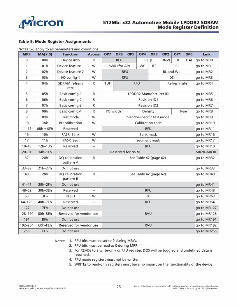
Table 9: Mode Register Assignments
Notes 1–5 apply to all parameters and conditionsMR# MA[7:0] Function Access OP7 OP6 OP5 OP4 OP3 OP2 OP1 OP0 Link
0 00h Device info R RFU RZQI DNVI DI DAI go to MR0
1 01h Device feature 1 W nWR (for AP) WC BT BL go to MR1
2 02h Device feature 2 W RFU RL and WL go to MR2
3 03h I/O config-1 W RFU DS go to MR3
4 04h SDRAM refreshrate
R TUF RFU Refresh rate go to MR4
5 05h Basic config-1 R LPDDR2 Manufacturer ID go to MR5
6 06h Basic config-2 R Revision ID1 go to MR6
7 07h Basic config-3 R Revision ID2 go to MR7
8 08h Basic config-4 R I/O width Density Type go to MR8
9 09h Test mode W Vendor-specific test mode go to MR9
10 0Ah I/O calibration W Calibration code go to MR10
11–15 0Bh ≈ 0Fh Reserved – RFU go to MR11
16 10h PASR_Bank W Bank mask go to MR16
17 11h PASR_Seg W Segment mask go to MR17
18–19 12h–13h Reserved – RFU go to MR18
20–31 14h–1Fh Reserved for NVM MR20–MR30
32 20h DQ calibrationpattern A
R See Table 42 (page 62). go to MR32
33–39 21h–27h Do not use go to MR33
40 28h DQ calibrationpattern B
R See Table 42 (page 62). go to MR40
41–47 29h–2Fh Do not use go to MR41
48–62 30h–3Eh Reserved – RFU go to MR48
63 3Fh RESET W X go to MR63
64–126 40h–7Eh Reserved – RFU go to MR64
127 7Fh Do not use go to MR127
128–190 80h–BEh Reserved for vendor use RVU go to MR128
191 BFh Do not use go to MR191
192–254 C0h–FEh Reserved for vendor use RVU go to MR192
255 FFh Do not use go to MR255
Notes: 1. RFU bits must be set to 0 during MRW.2. RFU bits must be read as 0 during MRR.3. For READs to a write-only or RFU register, DQS will be toggled and undefined data is
returned.4. RFU mode registers must not be written.5. WRITEs to read-only registers must have no impact on the functionality of the device.
512Mb: x32 Automotive Mobile LPDDR2 SDRAMMode Register Definition
09005aef86573be0u97m_auto_lpddr2_ait_aat_aut.pdf - Rev. H 05/18 EN 25 Micron Technology, Inc. reserves the right to change products or specifications without notice.
© 2015 Micron Technology, Inc. All rights reserved.
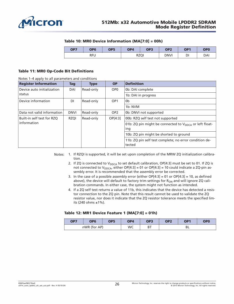
Table 10: MR0 Device Information (MA[7:0] = 00h)
OP7 OP6 OP5 OP4 OP3 OP2 OP1 OP0
RFU RZQI DNVI DI DAI
Table 11: MR0 Op-Code Bit Definitions
Notes 1–4 apply to all parameters and conditionsRegister Information Tag Type OP Definition
Device auto initializationstatus
DAI Read-only OP0 0b: DAI complete
1b: DAI in progress
Device information DI Read-only OP1 0b
1b: NVM
Data not valid information DNVI Read-only OP2 0b: DNVI not supported
Built-in self test for RZQinformation
RZQI Read-only OP[4:3] 00b: RZQ self test not supported
01b: ZQ pin might be connected to VDDCA or left float-ing
10b: ZQ pin might be shorted to ground
11b: ZQ pin self test complete; no error condition de-tected
Notes: 1. If RZQI is supported, it will be set upon completion of the MRW ZQ initialization calibra-tion.
2. If ZQ is connected to VDDCA to set default calibration, OP[4:3] must be set to 01. If ZQ isnot connected to VDDCA, either OP[4:3] = 01 or OP[4:3] = 10 could indicate a ZQ-pin as-sembly error. It is recommended that the assembly error be corrected.
3. In the case of a possible assembly error (either OP[4:3] = 01 or OP[4:3] = 10, as definedabove), the device will default to factory trim settings for RON and will ignore ZQ cali-bration commands. In either case, the system might not function as intended.
4. If a ZQ self test returns a value of 11b, this indicates that the device has detected a resis-tor connection to the ZQ pin. Note that this result cannot be used to validate the ZQresistor value, nor does it indicate that the ZQ resistor tolerance meets the specified lim-its (240 ohms ±1%).
Table 12: MR1 Device Feature 1 (MA[7:0] = 01h)
OP7 OP6 OP5 OP4 OP3 OP2 OP1 OP0
nWR (for AP) WC BT BL
512Mb: x32 Automotive Mobile LPDDR2 SDRAMMode Register Definition
09005aef86573be0u97m_auto_lpddr2_ait_aat_aut.pdf - Rev. H 05/18 EN 26 Micron Technology, Inc. reserves the right to change products or specifications without notice.
© 2015 Micron Technology, Inc. All rights reserved.
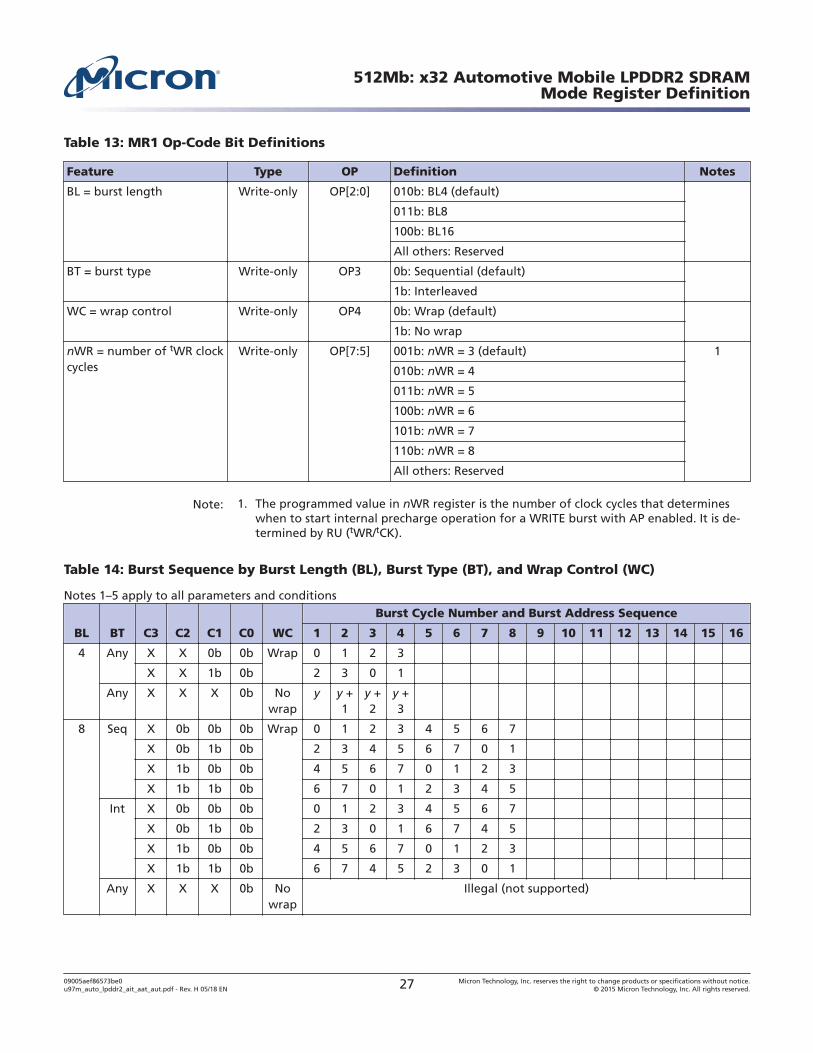
Table 13: MR1 Op-Code Bit Definitions
Feature Type OP Definition Notes
BL = burst length Write-only OP[2:0] 010b: BL4 (default)
011b: BL8
100b: BL16
All others: Reserved
BT = burst type Write-only OP3 0b: Sequential (default)
1b: Interleaved
WC = wrap control Write-only OP4 0b: Wrap (default)
1b: No wrap
nWR = number of tWR clockcycles
Write-only OP[7:5] 001b: nWR = 3 (default) 1
010b: nWR = 4
011b: nWR = 5
100b: nWR = 6
101b: nWR = 7
110b: nWR = 8
All others: Reserved
Note: 1. The programmed value in nWR register is the number of clock cycles that determineswhen to start internal precharge operation for a WRITE burst with AP enabled. It is de-termined by RU (tWR/tCK).
Table 14: Burst Sequence by Burst Length (BL), Burst Type (BT), and Wrap Control (WC)
Notes 1–5 apply to all parameters and conditions
BL BT C3 C2 C1 C0 WC
Burst Cycle Number and Burst Address Sequence
1 2 3 4 5 6 7 8 9 10 11 12 13 14 15 16
4 Any X X 0b 0b Wrap 0 1 2 3
X X 1b 0b 2 3 0 1
Any X X X 0b Nowrap
y y +1
y +2
y +3
8 Seq X 0b 0b 0b Wrap 0 1 2 3 4 5 6 7
X 0b 1b 0b 2 3 4 5 6 7 0 1
X 1b 0b 0b 4 5 6 7 0 1 2 3
X 1b 1b 0b 6 7 0 1 2 3 4 5
Int X 0b 0b 0b 0 1 2 3 4 5 6 7
X 0b 1b 0b 2 3 0 1 6 7 4 5
X 1b 0b 0b 4 5 6 7 0 1 2 3
X 1b 1b 0b 6 7 4 5 2 3 0 1
Any X X X 0b Nowrap
Illegal (not supported)
512Mb: x32 Automotive Mobile LPDDR2 SDRAMMode Register Definition
09005aef86573be0u97m_auto_lpddr2_ait_aat_aut.pdf - Rev. H 05/18 EN 27 Micron Technology, Inc. reserves the right to change products or specifications without notice.
© 2015 Micron Technology, Inc. All rights reserved.
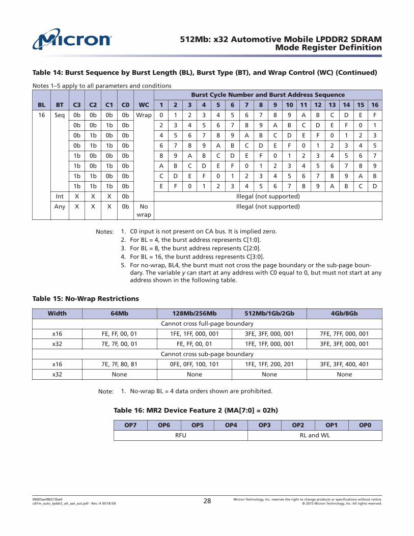
Table 14: Burst Sequence by Burst Length (BL), Burst Type (BT), and Wrap Control (WC) (Continued)
Notes 1–5 apply to all parameters and conditions
BL BT C3 C2 C1 C0 WC
Burst Cycle Number and Burst Address Sequence
1 2 3 4 5 6 7 8 9 10 11 12 13 14 15 16
16 Seq 0b 0b 0b 0b Wrap 0 1 2 3 4 5 6 7 8 9 A B C D E F
0b 0b 1b 0b 2 3 4 5 6 7 8 9 A B C D E F 0 1
0b 1b 0b 0b 4 5 6 7 8 9 A B C D E F 0 1 2 3
0b 1b 1b 0b 6 7 8 9 A B C D E F 0 1 2 3 4 5
1b 0b 0b 0b 8 9 A B C D E F 0 1 2 3 4 5 6 7
1b 0b 1b 0b A B C D E F 0 1 2 3 4 5 6 7 8 9
1b 1b 0b 0b C D E F 0 1 2 3 4 5 6 7 8 9 A B
1b 1b 1b 0b E F 0 1 2 3 4 5 6 7 8 9 A B C D
Int X X X 0b Illegal (not supported)
Any X X X 0b Nowrap
Illegal (not supported)
Notes: 1. C0 input is not present on CA bus. It is implied zero.2. For BL = 4, the burst address represents C[1:0].3. For BL = 8, the burst address represents C[2:0].4. For BL = 16, the burst address represents C[3:0].5. For no-wrap, BL4, the burst must not cross the page boundary or the sub-page boun-
dary. The variable y can start at any address with C0 equal to 0, but must not start at anyaddress shown in the following table.
Table 15: No-Wrap Restrictions
Width 64Mb 128Mb/256Mb 512Mb/1Gb/2Gb 4Gb/8Gb
Cannot cross full-page boundary
x16 FE, FF, 00, 01 1FE, 1FF, 000, 001 3FE, 3FF, 000, 001 7FE, 7FF, 000, 001
x32 7E, 7F, 00, 01 FE, FF, 00, 01 1FE, 1FF, 000, 001 3FE, 3FF, 000, 001
Cannot cross sub-page boundary
x16 7E, 7F, 80, 81 0FE, 0FF, 100, 101 1FE, 1FF, 200, 201 3FE, 3FF, 400, 401
x32 None None None None
Note: 1. No-wrap BL = 4 data orders shown are prohibited.
Table 16: MR2 Device Feature 2 (MA[7:0] = 02h)
OP7 OP6 OP5 OP4 OP3 OP2 OP1 OP0
RFU RL and WL
512Mb: x32 Automotive Mobile LPDDR2 SDRAMMode Register Definition
09005aef86573be0u97m_auto_lpddr2_ait_aat_aut.pdf - Rev. H 05/18 EN 28 Micron Technology, Inc. reserves the right to change products or specifications without notice.
© 2015 Micron Technology, Inc. All rights reserved.
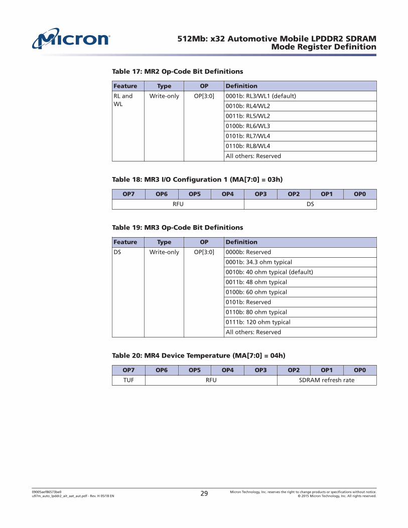
Table 17: MR2 Op-Code Bit Definitions
Feature Type OP Definition
RL andWL
Write-only OP[3:0] 0001b: RL3/WL1 (default)
0010b: RL4/WL2
0011b: RL5/WL2
0100b: RL6/WL3
0101b: RL7/WL4
0110b: RL8/WL4
All others: Reserved
Table 18: MR3 I/O Configuration 1 (MA[7:0] = 03h)
OP7 OP6 OP5 OP4 OP3 OP2 OP1 OP0
RFU DS
Table 19: MR3 Op-Code Bit Definitions
Feature Type OP Definition
DS Write-only OP[3:0] 0000b: Reserved
0001b: 34.3 ohm typical
0010b: 40 ohm typical (default)
0011b: 48 ohm typical
0100b: 60 ohm typical
0101b: Reserved
0110b: 80 ohm typical
0111b: 120 ohm typical
All others: Reserved
Table 20: MR4 Device Temperature (MA[7:0] = 04h)
OP7 OP6 OP5 OP4 OP3 OP2 OP1 OP0
TUF RFU SDRAM refresh rate
512Mb: x32 Automotive Mobile LPDDR2 SDRAMMode Register Definition
09005aef86573be0u97m_auto_lpddr2_ait_aat_aut.pdf - Rev. H 05/18 EN 29 Micron Technology, Inc. reserves the right to change products or specifications without notice.
© 2015 Micron Technology, Inc. All rights reserved.
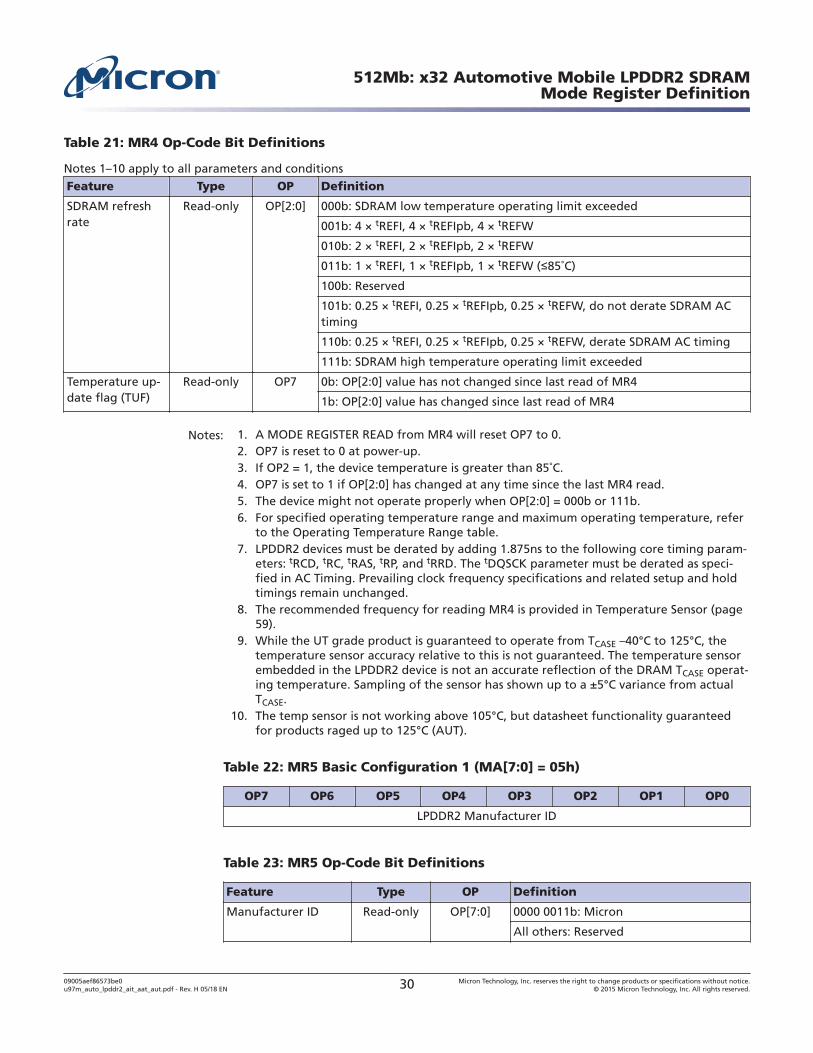
Table 21: MR4 Op-Code Bit Definitions
Notes 1–10 apply to all parameters and conditionsFeature Type OP Definition
SDRAM refreshrate
Read-only OP[2:0] 000b: SDRAM low temperature operating limit exceeded
001b: 4 × tREFI, 4 × tREFIpb, 4 × tREFW
010b: 2 × tREFI, 2 × tREFIpb, 2 × tREFW
011b: 1 × tREFI, 1 × tREFIpb, 1 × tREFW (≤85˚C)
100b: Reserved
101b: 0.25 × tREFI, 0.25 × tREFIpb, 0.25 × tREFW, do not derate SDRAM ACtiming
110b: 0.25 × tREFI, 0.25 × tREFIpb, 0.25 × tREFW, derate SDRAM AC timing
111b: SDRAM high temperature operating limit exceeded
Temperature up-date flag (TUF)
Read-only OP7 0b: OP[2:0] value has not changed since last read of MR4
1b: OP[2:0] value has changed since last read of MR4
Notes: 1. A MODE REGISTER READ from MR4 will reset OP7 to 0.2. OP7 is reset to 0 at power-up.3. If OP2 = 1, the device temperature is greater than 85˚C.4. OP7 is set to 1 if OP[2:0] has changed at any time since the last MR4 read.5. The device might not operate properly when OP[2:0] = 000b or 111b.6. For specified operating temperature range and maximum operating temperature, refer
to the Operating Temperature Range table.7. LPDDR2 devices must be derated by adding 1.875ns to the following core timing param-
eters: tRCD, tRC, tRAS, tRP, and tRRD. The tDQSCK parameter must be derated as speci-fied in AC Timing. Prevailing clock frequency specifications and related setup and holdtimings remain unchanged.
8. The recommended frequency for reading MR4 is provided in Temperature Sensor (page59).
9. While the UT grade product is guaranteed to operate from TCASE –40°C to 125°C, thetemperature sensor accuracy relative to this is not guaranteed. The temperature sensorembedded in the LPDDR2 device is not an accurate reflection of the DRAM TCASE operat-ing temperature. Sampling of the sensor has shown up to a ±5°C variance from actualTCASE.
10. The temp sensor is not working above 105°C, but datasheet functionality guaranteedfor products raged up to 125°C (AUT).
Table 22: MR5 Basic Configuration 1 (MA[7:0] = 05h)
OP7 OP6 OP5 OP4 OP3 OP2 OP1 OP0
LPDDR2 Manufacturer ID
Table 23: MR5 Op-Code Bit Definitions
Feature Type OP Definition
Manufacturer ID Read-only OP[7:0] 0000 0011b: Micron
All others: Reserved
512Mb: x32 Automotive Mobile LPDDR2 SDRAMMode Register Definition
09005aef86573be0u97m_auto_lpddr2_ait_aat_aut.pdf - Rev. H 05/18 EN 30 Micron Technology, Inc. reserves the right to change products or specifications without notice.
© 2015 Micron Technology, Inc. All rights reserved.
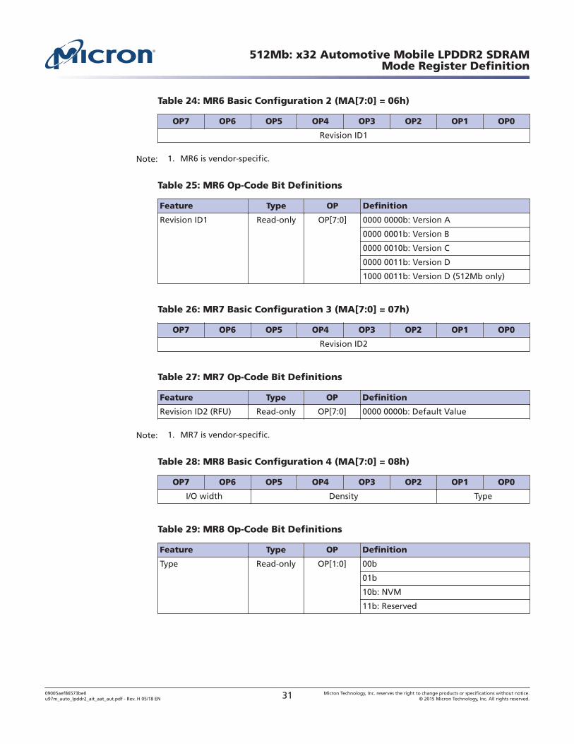
Table 24: MR6 Basic Configuration 2 (MA[7:0] = 06h)
OP7 OP6 OP5 OP4 OP3 OP2 OP1 OP0
Revision ID1
Note: 1. MR6 is vendor-specific.
Table 25: MR6 Op-Code Bit Definitions
Feature Type OP Definition
Revision ID1 Read-only OP[7:0] 0000 0000b: Version A
0000 0001b: Version B
0000 0010b: Version C
0000 0011b: Version D
1000 0011b: Version D (512Mb only)
Table 26: MR7 Basic Configuration 3 (MA[7:0] = 07h)
OP7 OP6 OP5 OP4 OP3 OP2 OP1 OP0
Revision ID2
Table 27: MR7 Op-Code Bit Definitions
Feature Type OP Definition
Revision ID2 (RFU) Read-only OP[7:0] 0000 0000b: Default Value
Note: 1. MR7 is vendor-specific.
Table 28: MR8 Basic Configuration 4 (MA[7:0] = 08h)
OP7 OP6 OP5 OP4 OP3 OP2 OP1 OP0
I/O width Density Type
Table 29: MR8 Op-Code Bit Definitions
Feature Type OP Definition
Type Read-only OP[1:0] 00b
01b
10b: NVM
11b: Reserved
512Mb: x32 Automotive Mobile LPDDR2 SDRAMMode Register Definition
09005aef86573be0u97m_auto_lpddr2_ait_aat_aut.pdf - Rev. H 05/18 EN 31 Micron Technology, Inc. reserves the right to change products or specifications without notice.
© 2015 Micron Technology, Inc. All rights reserved.
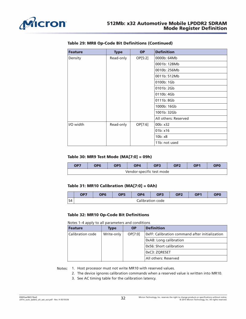
Table 29: MR8 Op-Code Bit Definitions (Continued)
Feature Type OP Definition
Density Read-only OP[5:2] 0000b: 64Mb
0001b: 128Mb
0010b: 256Mb
0011b: 512Mb
0100b: 1Gb
0101b: 2Gb
0110b: 4Gb
0111b: 8Gb
1000b: 16Gb
1001b: 32Gb
All others: Reserved
I/O width Read-only OP[7:6] 00b: x32
01b: x16
10b: x8
11b: not used
Table 30: MR9 Test Mode (MA[7:0] = 09h)
OP7 OP6 OP5 OP4 OP3 OP2 OP1 OP0
Vendor-specific test mode
Table 31: MR10 Calibration (MA[7:0] = 0Ah)
OP7 OP6 OP5 OP4 OP3 OP2 OP1 OP0
S4 Calibration code
Table 32: MR10 Op-Code Bit Definitions
Notes 1–4 apply to all parameters and conditionsFeature Type OP Definition
Calibration code Write-only OP[7:0] 0xFF: Calibration command after initialization
0xAB: Long calibration
0x56: Short calibration
0xC3: ZQRESET
All others: Reserved
Notes: 1. Host processor must not write MR10 with reserved values.2. The device ignores calibration commands when a reserved value is written into MR10.3. See AC timing table for the calibration latency.
512Mb: x32 Automotive Mobile LPDDR2 SDRAMMode Register Definition
09005aef86573be0u97m_auto_lpddr2_ait_aat_aut.pdf - Rev. H 05/18 EN 32 Micron Technology, Inc. reserves the right to change products or specifications without notice.
© 2015 Micron Technology, Inc. All rights reserved.
4. If ZQ is connected to VSSCA through RZQ, either the ZQ calibration function (see MRW ZQCalibration Commands (page 64)) or default calibration (through the ZQRESET com-mand) is supported. If ZQ is connected to VDDCA, the device operates with default cali-bration, and ZQ calibration commands are ignored. In both cases, the ZQ connectionmust not change after power is supplied to the device.
Table 33: MR[11:15] Reserved (MA[7:0] = 0Bh–0Fh)
OP7 OP6 OP5 OP4 OP3 OP2 OP1 OP0
Reserved
Table 34: MR16 PASR Bank Mask (MA[7:0] = 010h)
OP7 OP6 OP5 OP4 OP3 OP2 OP1 OP0
Bank mask (4-bank)
Table 35: MR16 Op-Code Bit Definitions
Feature Type OP Definition
Bank[3:0] mask Write-only OP[3:0] 0b: refresh enable to the bank = unmasked (default)
1b: refresh blocked = masked
Table 36: MR17 PASR Segment Mask (MA[7:0] = 011h)
OP7 OP6 OP5 OP4 OP3 OP2 OP1 OP0
Segment mask
Note: 1. This table applies for 1Gb to 8Gb devices only.
512Mb: x32 Automotive Mobile LPDDR2 SDRAMMode Register Definition
09005aef86573be0u97m_auto_lpddr2_ait_aat_aut.pdf - Rev. H 05/18 EN 33 Micron Technology, Inc. reserves the right to change products or specifications without notice.
© 2015 Micron Technology, Inc. All rights reserved.
Table 37: Reserved Mode Registers
Mode Reg-ister MA Address Restriction OP7 OP6 OP5 OP4 OP3 OP2 OP1 OP0
MR[18:19] MA[7:0] 12h–13h RFU Reserved
MR[20:31] 14h–1Fh NVM1
MR[33:39] 21h–27h DNU1
MR[41:47] 29h–2Fh
MR[48:62] 30h–3Eh RFU
MR[64:126] 40h–7Eh RFU
MR127 7Fh DNU
MR[128:190] 80h–BEh RVU1
MR191 BFh DNU
MR[192:254] C0h–FEh RVU
MR255 FFh DNU
Note: 1. NVM = nonvolatile memory use only; DNU = Do not use; RVU = Reserved for vendor use.
Table 38: MR63 RESET (MA[7:0] = 3Fh) – MRW Only
OP7 OP6 OP5 OP4 OP3 OP2 OP1 OP0
X
Note: 1. For additional information on MRW RESET see MODE REGISTER WRITE Command (page63).
512Mb: x32 Automotive Mobile LPDDR2 SDRAMMode Register Definition
09005aef86573be0u97m_auto_lpddr2_ait_aat_aut.pdf - Rev. H 05/18 EN 34 Micron Technology, Inc. reserves the right to change products or specifications without notice.
© 2015 Micron Technology, Inc. All rights reserved.
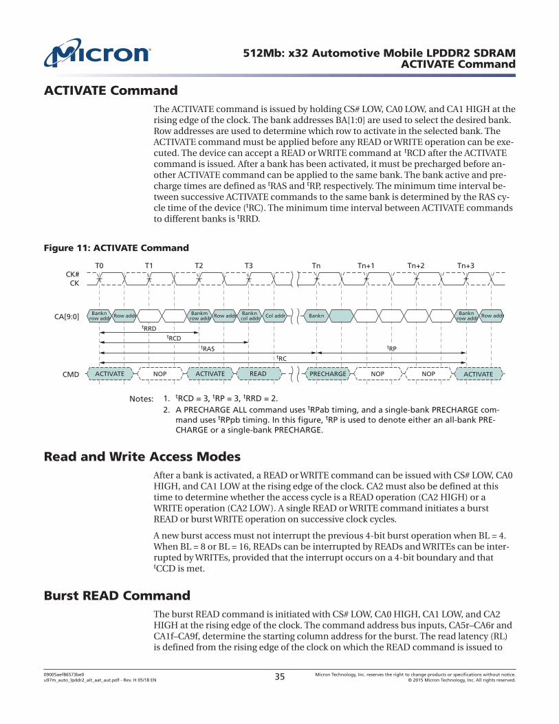
ACTIVATE CommandThe ACTIVATE command is issued by holding CS# LOW, CA0 LOW, and CA1 HIGH at therising edge of the clock. The bank addresses BA[1:0] are used to select the desired bank.Row addresses are used to determine which row to activate in the selected bank. TheACTIVATE command must be applied before any READ or WRITE operation can be exe-cuted. The device can accept a READ or WRITE command at tRCD after the ACTIVATEcommand is issued. After a bank has been activated, it must be precharged before an-other ACTIVATE command can be applied to the same bank. The bank active and pre-charge times are defined as tRAS and tRP, respectively. The minimum time interval be-tween successive ACTIVATE commands to the same bank is determined by the RAS cy-cle time of the device (tRC). The minimum time interval between ACTIVATE commandsto different banks is tRRD.
Figure 11: ACTIVATE Command
Bank nrow addr Row addr
ACTIVATE NOP ACTIVATE READ PRECHARGE ACTIVATENOP NOP
Bank mrow addr Row addr Bank n
col addr Col addr Bank n Bank nrow addr Row addr
T0 T1 T2 T3 Tn Tn+1 Tn+2 Tn+3CK#CK
CA[9:0]
CMD
tRRDtRCD
tRC
tRAS tRP
Notes: 1. tRCD = 3, tRP = 3, tRRD = 2.2. A PRECHARGE ALL command uses tRPab timing, and a single-bank PRECHARGE com-
mand uses tRPpb timing. In this figure, tRP is used to denote either an all-bank PRE-CHARGE or a single-bank PRECHARGE.
Read and Write Access ModesAfter a bank is activated, a READ or WRITE command can be issued with CS# LOW, CA0HIGH, and CA1 LOW at the rising edge of the clock. CA2 must also be defined at thistime to determine whether the access cycle is a READ operation (CA2 HIGH) or aWRITE operation (CA2 LOW). A single READ or WRITE command initiates a burstREAD or burst WRITE operation on successive clock cycles.
A new burst access must not interrupt the previous 4-bit burst operation when BL = 4.When BL = 8 or BL = 16, READs can be interrupted by READs and WRITEs can be inter-rupted by WRITEs, provided that the interrupt occurs on a 4-bit boundary and thattCCD is met.
Burst READ CommandThe burst READ command is initiated with CS# LOW, CA0 HIGH, CA1 LOW, and CA2HIGH at the rising edge of the clock. The command address bus inputs, CA5r–CA6r andCA1f–CA9f, determine the starting column address for the burst. The read latency (RL)is defined from the rising edge of the clock on which the READ command is issued to
512Mb: x32 Automotive Mobile LPDDR2 SDRAMACTIVATE Command
09005aef86573be0u97m_auto_lpddr2_ait_aat_aut.pdf - Rev. H 05/18 EN 35 Micron Technology, Inc. reserves the right to change products or specifications without notice.
© 2015 Micron Technology, Inc. All rights reserved.
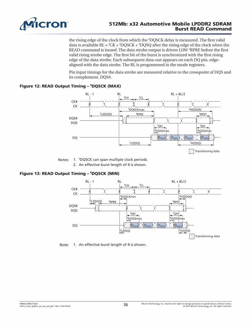
the rising edge of the clock from which the tDQSCK delay is measured. The first validdata is available RL × tCK + tDQSCK + tDQSQ after the rising edge of the clock when theREAD command is issued. The data strobe output is driven LOW tRPRE before the firstvalid rising strobe edge. The first bit of the burst is synchronized with the first risingedge of the data strobe. Each subsequent data-out appears on each DQ pin, edge-aligned with the data strobe. The RL is programmed in the mode registers.
Pin input timings for the data strobe are measured relative to the crosspoint of DQS andits complement, DQS#.
Figure 12: READ Output Timing – tDQSCK (MAX)
RL - 1 RL RL + BL/2
CK#CK
DQS#DQS
DQ
tLZ(DQS)
DOUT DOUT DOUT DOUT
tHZ(DQS)tRPRE tRPST
tDQSCKmax
tQH
tLZ(DQ) tHZ(DQ)
tDQSQmax
tCLtCH
tQHtDQSQmax
Transitioning data
Notes: 1. tDQSCK can span multiple clock periods.2. An effective burst length of 4 is shown.
Figure 13: READ Output Timing – tDQSCK (MIN)
RL - 1 RL RL + BL/2
CK#CK
DQS#DQS
DQ
tLZ(DQS)
DOUT DOUT DOUT DOUT
tHZ(DQS)tRPRE
tDQSCKmin
tQH
tLZ(DQ)
tDQSQmax
tCLtCH
tQHtDQSQmax
tRPST
tHZ(DQ)
Transitioning data
Note: 1. An effective burst length of 4 is shown.
512Mb: x32 Automotive Mobile LPDDR2 SDRAMBurst READ Command
09005aef86573be0u97m_auto_lpddr2_ait_aat_aut.pdf - Rev. H 05/18 EN 36 Micron Technology, Inc. reserves the right to change products or specifications without notice.
© 2015 Micron Technology, Inc. All rights reserved.
Figure 14: Burst READ – RL = 5, BL = 4, tDQSCK > tCK
Bank ncol addr Col addr
READ NOP
T0 T1 T2 T3 T4 T5 T6 T7 T8
CA[9:0]
CMD
DQS#DQS
DQ
RL = 5
Transitioning data
NOP NOP NOP NOP
tDQSCK
NOP
DOUT A0 DOUT A1 DOUT A2 DOUT A3
NOP NOP
CK#CK
Figure 15: Burst READ – RL = 3, BL = 8, tDQSCK < tCK
Bank ncol addr Col addr
READ NOP
T0 T1 T2 T3 T4 T5 T6 T7 T8CK#
CK
CA[9:0]
CMD
DQS#DQS
DQ
RL = 3
Transitioning data
NOP NOP NOP NOP
tDQSCK
NOP
DOUT A4 DOUT A5 DOUT A6 DOUT A7DOUT A0 DOUT A1 DOUT A2 DOUT A3
NOP NOP
512Mb: x32 Automotive Mobile LPDDR2 SDRAMBurst READ Command
09005aef86573be0u97m_auto_lpddr2_ait_aat_aut.pdf - Rev. H 05/18 EN 37 Micron Technology, Inc. reserves the right to change products or specifications without notice.
© 2015 Micron Technology, Inc. All rights reserved.
Figure 16: tDQSCKDL Timing
Col addrBank ncol addr
READ NOP
Tm Tm + 1 Tm + 2 Tm + 3 Tm + 4 Tm + 5 Tm + 6 Tm + 7 Tm + 8
CA[9:0]
CMD
DQS#DQS
DQ
RL = 5
Transitioning data
NOP NOP NOP NOP
tDQSCKm
NOP
DOUT A0 DOUT A1 DOUT A2 DOUT A3
NOP NOP
CK#CK
1
Col addrBank ncol addr
READ NOP
Tn Tn + 1 Tn + 2 Tn + 3 Tn + 4 Tn + 5 Tn + 6 Tn + 7 Tn + 8
CA[9:0]
CMD
DQS#DQS
DQ
RL = 5
…32ms maximum
32ms maximum…
NOP NOP NOP NOP
tDQSCKn
NOP
DOUT A0 DOUT A1 DOUT A2 DOUT A3
NOP NOP
CK#CK
1
Notes: 1. tDQSCKDL = (tDQSCKn - tDQSCKm).2. tDQSCKDL (MAX) is defined as the maximum of ABS (tDQSCKn - tDQSCKm) for any
(tDQSCKn, tDQSCKm) pair within any 32ms rolling window.
512Mb: x32 Automotive Mobile LPDDR2 SDRAMBurst READ Command
09005aef86573be0u97m_auto_lpddr2_ait_aat_aut.pdf - Rev. H 05/18 EN 38 Micron Technology, Inc. reserves the right to change products or specifications without notice.
© 2015 Micron Technology, Inc. All rights reserved.
Figure 17: tDQSCKDM Timing
Col addrBank ncol addr
READ NOP
Tm Tm + 1 Tm + 2 Tm + 3 Tm + 4 Tm + 5 Tm + 6 Tm + 7 Tm + 8
CA[9:0]
CMD
DQS#DQS
DQ
RL = 5
Transitioning data
NOP NOP NOP NOP
tDQSCKm
NOP
DOUT A0 DOUT A1 DOUT A2 DOUT A3
NOP NOP
CK#CK
1
Col addrBank ncol addr
READ NOP
Tn Tn + 1 Tn + 2 Tn + 3 Tn + 4 Tn + 5 Tn + 6 Tn + 7 Tn + 8
CA[9:0]
CMD
DQS#DQS
DQ
RL = 5
…1.6μs maximum
1.6μs maximum…
NOP NOP NOP NOP
tDQSCKn
NOP
DOUT A0 DOUT A1 DOUT A2 DOUT A3
NOP NOP
CK#CK
1
Notes: 1. tDQSCKDM = (tDQSCKn - tDQSCKm).2. tDQSCKDM (MAX) is defined as the maximum of ABS (tDQSCKn - tDQSCKm) for any
(tDQSCKn, tDQSCKm) pair within any 1.6μs rolling window.
512Mb: x32 Automotive Mobile LPDDR2 SDRAMBurst READ Command
09005aef86573be0u97m_auto_lpddr2_ait_aat_aut.pdf - Rev. H 05/18 EN 39 Micron Technology, Inc. reserves the right to change products or specifications without notice.
© 2015 Micron Technology, Inc. All rights reserved.
Figure 18: tDQSCKDS Timing
Col addrBank ncol addr
READ NOP
Tm Tm + 1 Tm + 2 Tm + 3 Tm + 4 Tm + 5 Tm + 6 Tm + 7 Tm + 8
CA[9:0]
CMD
DQS#DQS
DQ
RL = 5
Transitioning data
NOP NOP NOP NOP
tDQSCKm
NOP
DOUT A0 DOUT A1 DOUT A2 DOUT A3DOUT A0 DOUT A1 DOUT A2 DOUT A3DOUT A0 DOUT A1 DOUT A2 DOUT A3DOUT A0 DOUT A1 DOUT A2 DOUT A3DOUT A2 DOUT A3
NOP NOP
CK#CK
1
Col addrBank ncol addr
READ NOP
Tn Tn + 1 Tn + 2 Tn + 3 Tn + 4 Tn + 5 Tn + 6 Tn + 7 Tn + 8
CA[9:0]
CMD
DQS#DQS
DQ
RL = 5
…160ns maximum
160ns maximum…
NOP NOP NOP NOP
tDQSCKn
NOP
DOUT A0 DOUT A1 DOUT A2 DOUT A3 DOUT A4
NOP NOP
CK#CK
1
Notes: 1. tDQSCKDS = (tDQSCKn - tDQSCKm).2. tDQSCKDS (MAX) is defined as the maximum of ABS (tDQSCKn - tDQSCKm) for any
(tDQSCKn, tDQSCKm) pair for READs within a consecutive burst, within any 160ns rollingwindow.
512Mb: x32 Automotive Mobile LPDDR2 SDRAMBurst READ Command
09005aef86573be0u97m_auto_lpddr2_ait_aat_aut.pdf - Rev. H 05/18 EN 40 Micron Technology, Inc. reserves the right to change products or specifications without notice.
© 2015 Micron Technology, Inc. All rights reserved.
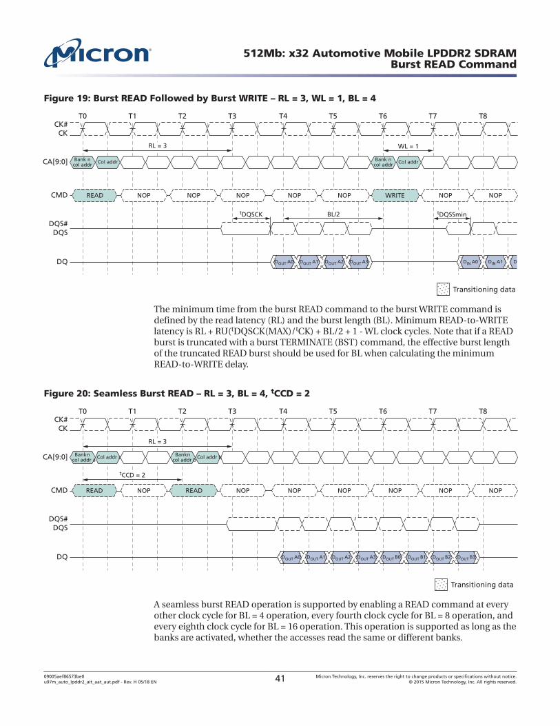
Figure 19: Burst READ Followed by Burst WRITE – RL = 3, WL = 1, BL = 4
Bank ncol addr Col addr
READ NOP
T0 T1 T2 T3 T4 T5 T6 T7 T8CK#
CK
CA[9:0]
CMD
DQS#DQS
DQ
RL = 3 WL = 1
BL/2
Transitioning data
NOP NOP NOP NOP
tDQSCK tDQSSmin
WRITE
DIN A0 DIN A1 DDOUT A0 DOUT A1 DOUT A2 DOUT A3
NOP NOP
Bank ncol addr Col addr
The minimum time from the burst READ command to the burst WRITE command isdefined by the read latency (RL) and the burst length (BL). Minimum READ-to-WRITElatency is RL + RU(tDQSCK(MAX)/tCK) + BL/2 + 1 - WL clock cycles. Note that if a READburst is truncated with a burst TERMINATE (BST) command, the effective burst lengthof the truncated READ burst should be used for BL when calculating the minimumREAD-to-WRITE delay.
Figure 20: Seamless Burst READ – RL = 3, BL = 4, tCCD = 2
Bank ncol addr a Col addr a
READ NOP
T0 T1 T2 T3 T4 T5 T6 T7 T8CK#
CK
CA[9:0]
CMD
DQS#DQS
DQ
RL = 3
Transitioning data
READ NOP NOP NOP
tCCD = 2
NOP
DOUT B0 DOUT B1 DOUT B2 DOUT B3DOUT A0 DOUT A1 DOUT A2 DOUT A3
NOP NOP
Bank ncol addr b Col addr b
A seamless burst READ operation is supported by enabling a READ command at everyother clock cycle for BL = 4 operation, every fourth clock cycle for BL = 8 operation, andevery eighth clock cycle for BL = 16 operation. This operation is supported as long as thebanks are activated, whether the accesses read the same or different banks.
512Mb: x32 Automotive Mobile LPDDR2 SDRAMBurst READ Command
09005aef86573be0u97m_auto_lpddr2_ait_aat_aut.pdf - Rev. H 05/18 EN 41 Micron Technology, Inc. reserves the right to change products or specifications without notice.
© 2015 Micron Technology, Inc. All rights reserved.
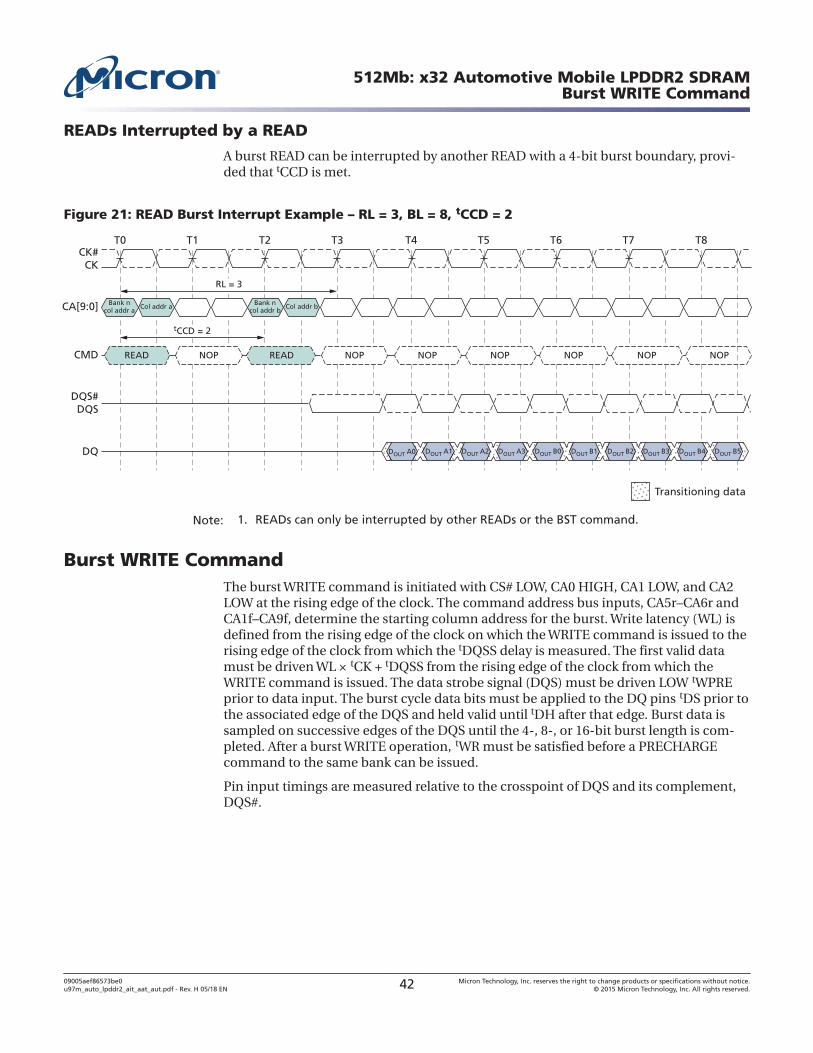
READs Interrupted by a READ
A burst READ can be interrupted by another READ with a 4-bit burst boundary, provi-ded that tCCD is met.
Figure 21: READ Burst Interrupt Example – RL = 3, BL = 8, tCCD = 2
READ NOP
T0 T1 T2 T3 T4 T5 T6 T7 T8CK#
CK
CA[9:0]
CMD
DQS#DQS
DQ
RL = 3
Transitioning data
READ NOP NOP NOP
tCCD = 2
NOP
DOUT B0 DOUT B1 DOUT B2 DOUT B3 DOUT B4 DOUT B5DOUT A0 DOUT A1 DOUT A2 DOUT A3
NOP NOP
Bank ncol addr a Col addr a Bank n
col addr b Col addr b
Note: 1. READs can only be interrupted by other READs or the BST command.
Burst WRITE CommandThe burst WRITE command is initiated with CS# LOW, CA0 HIGH, CA1 LOW, and CA2LOW at the rising edge of the clock. The command address bus inputs, CA5r–CA6r andCA1f–CA9f, determine the starting column address for the burst. Write latency (WL) isdefined from the rising edge of the clock on which the WRITE command is issued to therising edge of the clock from which the tDQSS delay is measured. The first valid datamust be driven WL × tCK + tDQSS from the rising edge of the clock from which theWRITE command is issued. The data strobe signal (DQS) must be driven LOW tWPREprior to data input. The burst cycle data bits must be applied to the DQ pins tDS prior tothe associated edge of the DQS and held valid until tDH after that edge. Burst data issampled on successive edges of the DQS until the 4-, 8-, or 16-bit burst length is com-pleted. After a burst WRITE operation, tWR must be satisfied before a PRECHARGEcommand to the same bank can be issued.
Pin input timings are measured relative to the crosspoint of DQS and its complement,DQS#.
512Mb: x32 Automotive Mobile LPDDR2 SDRAMBurst WRITE Command
09005aef86573be0u97m_auto_lpddr2_ait_aat_aut.pdf - Rev. H 05/18 EN 42 Micron Technology, Inc. reserves the right to change products or specifications without notice.
© 2015 Micron Technology, Inc. All rights reserved.
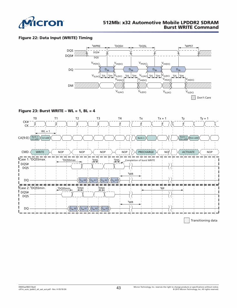
Figure 22: Data Input (WRITE) Timing
DQS
DQS#DQS#
DQS
DQ
DM
VIL(AC)
VIH(AC)
tDS
tWPRE tDQSH tDQSL tWPST
tDHtDS tDHtDH VIL(AC)
VIH(AC)
tDS
VIL(AC)
VIH(AC)
DIN DIN DIN DIN
VIL(DC)
VIH(DC)
VIL(DC)
VIH(DC)
tDH
VIL(DC)
VIH(DC)
tDS
VIL(AC)
VIH(AC)
VIL(DC)
VIH(DC)
Don’t Care
Figure 23: Burst WRITE – WL = 1, BL = 4
Bank ncol addr Col addr
WRITE NOP
T0 T1 T2 T3 T4 Tx Tx + 1 Ty Ty + 1CK#
CK
CA[9:0]
CMD
DQS#DQS
DQ
WL = 1
tWR
Completion of burst WRITE
Transitioning data
NOP NOP NOP PRECHARGE
tDQSSmax tDSS tDSS
NOP
DIN A0 DIN A1 DIN A2 DIN A3
ACTIVATE NOP
Bank n Bank nrow addr Row addr
DQS#DQS
DQ
tWR
tDQSSmin tDSH tDSH tRP
DIN A0 DIN A1 DIN A2 DIN A3
Case 1: tDQSSmax
Case 2: tDQSSmin
512Mb: x32 Automotive Mobile LPDDR2 SDRAMBurst WRITE Command
09005aef86573be0u97m_auto_lpddr2_ait_aat_aut.pdf - Rev. H 05/18 EN 43 Micron Technology, Inc. reserves the right to change products or specifications without notice.
© 2015 Micron Technology, Inc. All rights reserved.
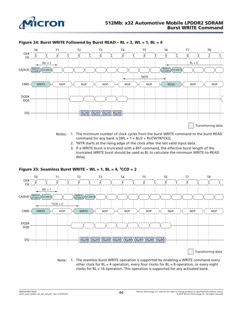
Figure 24: Burst WRITE Followed by Burst READ – RL = 3, WL = 1, BL = 4
Bank mcol addr a
Col addr a
WRITE NOP
T0 T1 T2 T3 T4 T5 T6 T7 T8CK#
CK
CA[9:0]
CMD
DQS#DQS
DQ
WL = 1 RL = 3
tWTR
Transitioning data
NOP NOP NOP NOP READ
DIN A0 DIN A1 DIN A2 DIN A3
NOP NOP
Bank ncol addr b Col addr b
Notes: 1. The minimum number of clock cycles from the burst WRITE command to the burst READcommand for any bank is [WL + 1 + BL/2 + RU(tWTR/tCK)].
2. tWTR starts at the rising edge of the clock after the last valid input data.3. If a WRITE burst is truncated with a BST command, the effective burst length of the
truncated WRITE burst should be used as BL to calculate the minimum WRITE-to-READdelay.
Figure 25: Seamless Burst WRITE – WL = 1, BL = 4, tCCD = 2
Bank mcol addr a Col addr a
WRITE NOP
T0 T1 T2 T3 T4 T5 T6 T7 T8CK#
CK
CA[9:0]
CMD
DQS#DQS
DQ
WL = 1
Transitioning data
WRITE NOP NOP NOP
tCCD = 2
NOP
DIN B0 DIN B1 DIN B2 DIN B3DIN A0 DIN A1 DIN A2 DIN A3
NOP NOP
Bank ncol addr b Col addr b
Note: 1. The seamless burst WRITE operation is supported by enabling a WRITE command everyother clock for BL = 4 operation, every four clocks for BL = 8 operation, or every eightclocks for BL = 16 operation. This operation is supported for any activated bank.
512Mb: x32 Automotive Mobile LPDDR2 SDRAMBurst WRITE Command
09005aef86573be0u97m_auto_lpddr2_ait_aat_aut.pdf - Rev. H 05/18 EN 44 Micron Technology, Inc. reserves the right to change products or specifications without notice.
© 2015 Micron Technology, Inc. All rights reserved.
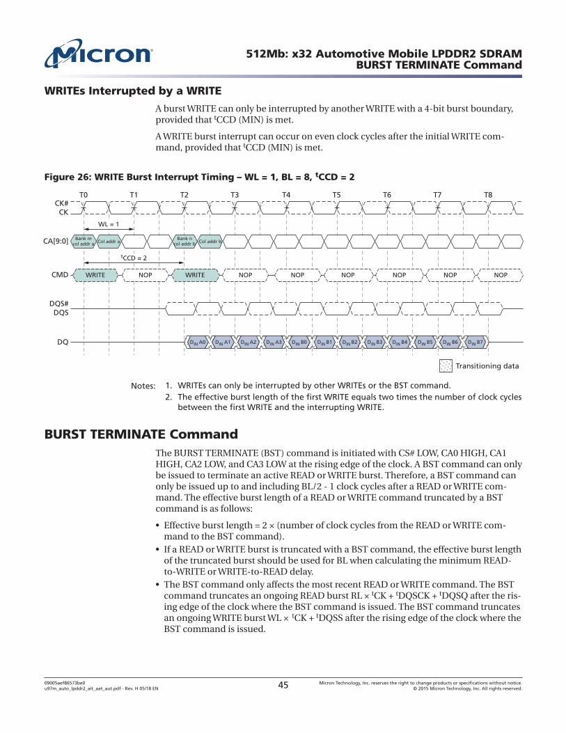
WRITEs Interrupted by a WRITE
A burst WRITE can only be interrupted by another WRITE with a 4-bit burst boundary,provided that tCCD (MIN) is met.
A WRITE burst interrupt can occur on even clock cycles after the initial WRITE com-mand, provided that tCCD (MIN) is met.
Figure 26: WRITE Burst Interrupt Timing – WL = 1, BL = 8, tCCD = 2
Bank mcol addr a Col addr a
WRITE NOP
T0 T1 T2 T3 T4 T5 T6 T7 T8CK#
CK
CA[9:0]
CMD
DQS#DQS
DQ
WL = 1
Transitioning data
WRITE NOP NOP NOP
tCCD = 2
NOP
DIN B0 DIN B1 DIN B2 DIN B3 DIN B4 DIN B5 DIN B6 DIN B7DIN A0 DIN A1 DIN A2 DIN A3
NOP NOP
Bank ncol addr b Col addr b
Notes: 1. WRITEs can only be interrupted by other WRITEs or the BST command.2. The effective burst length of the first WRITE equals two times the number of clock cycles
between the first WRITE and the interrupting WRITE.
BURST TERMINATE CommandThe BURST TERMINATE (BST) command is initiated with CS# LOW, CA0 HIGH, CA1HIGH, CA2 LOW, and CA3 LOW at the rising edge of the clock. A BST command can onlybe issued to terminate an active READ or WRITE burst. Therefore, a BST command canonly be issued up to and including BL/2 - 1 clock cycles after a READ or WRITE com-mand. The effective burst length of a READ or WRITE command truncated by a BSTcommand is as follows:
• Effective burst length = 2 × (number of clock cycles from the READ or WRITE com-mand to the BST command).
• If a READ or WRITE burst is truncated with a BST command, the effective burst lengthof the truncated burst should be used for BL when calculating the minimum READ-to-WRITE or WRITE-to-READ delay.
• The BST command only affects the most recent READ or WRITE command. The BSTcommand truncates an ongoing READ burst RL × tCK + tDQSCK + tDQSQ after the ris-ing edge of the clock where the BST command is issued. The BST command truncatesan ongoing WRITE burst WL × tCK + tDQSS after the rising edge of the clock where theBST command is issued.
512Mb: x32 Automotive Mobile LPDDR2 SDRAMBURST TERMINATE Command
09005aef86573be0u97m_auto_lpddr2_ait_aat_aut.pdf - Rev. H 05/18 EN 45 Micron Technology, Inc. reserves the right to change products or specifications without notice.
© 2015 Micron Technology, Inc. All rights reserved.
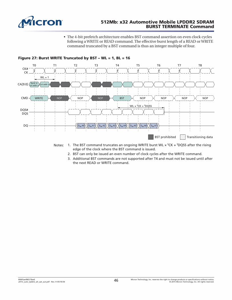
• The 4-bit prefetch architecture enables BST command assertion on even clock cyclesfollowing a WRITE or READ command. The effective burst length of a READ or WRITEcommand truncated by a BST command is thus an integer multiple of four.
Figure 27: Burst WRITE Truncated by BST – WL = 1, BL = 16
Bank mcol addr a Col addr a
WRITE NOP
T0 T1 T2 T3 T4 T5 T6 T7 T8CK#
CK
CA[9:0]
CMD
DQS#DQS
DQ
WL = 1
Transitioning dataBST prohibited
NOP NOP BST NOP
WL × tCK + tDQSS
NOP
DIN A4 DIN A5 DIN A6 DIN A7DIN A0 DIN A1 DIN A2 DIN A3
NOP NOP
Notes: 1. The BST command truncates an ongoing WRITE burst WL × tCK + tDQSS after the risingedge of the clock where the BST command is issued.
2. BST can only be issued an even number of clock cycles after the WRITE command.3. Additional BST commands are not supported after T4 and must not be issued until after
the next READ or WRITE command.
512Mb: x32 Automotive Mobile LPDDR2 SDRAMBURST TERMINATE Command
09005aef86573be0u97m_auto_lpddr2_ait_aat_aut.pdf - Rev. H 05/18 EN 46 Micron Technology, Inc. reserves the right to change products or specifications without notice.
© 2015 Micron Technology, Inc. All rights reserved.
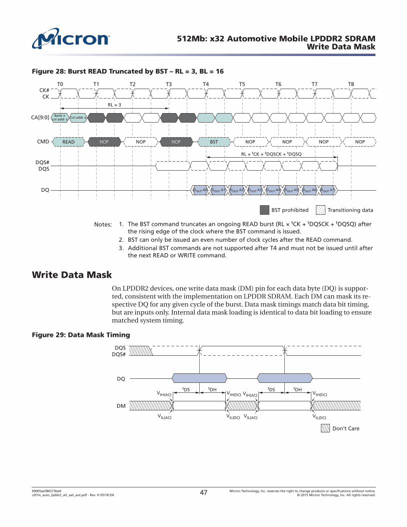
Figure 28: Burst READ Truncated by BST – RL = 3, BL = 16
Bank ncol addr a Col addr a
READ NOP
T0 T1 T2 T3 T4 T5 T6 T7 T8CK#
CK
CA[9:0]
CMD
DQS#DQS
DQ
RL = 3
Transitioning dataBST prohibited
NOP NOP BST NOP
RL × tCK + tDQSCK + tDQSQ
NOP
DOUT A4 DOUT A5 DOUT A6 DOUT A7DOUT A0 DOUT A1 DOUT A2 DOUT A3
NOP NOP
Notes: 1. The BST command truncates an ongoing READ burst (RL × tCK + tDQSCK + tDQSQ) afterthe rising edge of the clock where the BST command is issued.
2. BST can only be issued an even number of clock cycles after the READ command.3. Additional BST commands are not supported after T4 and must not be issued until after
the next READ or WRITE command.
Write Data MaskOn LPDDR2 devices, one write data mask (DM) pin for each data byte (DQ) is suppor-ted, consistent with the implementation on LPDDR SDRAM. Each DM can mask its re-spective DQ for any given cycle of the burst. Data mask timings match data bit timing,but are inputs only. Internal data mask loading is identical to data bit loading to ensurematched system timing.
Figure 29: Data Mask Timing
DQSDQS#
DQ
DM
tDS tDH tDS
VIL(AC)
VIH(AC)
VIL(AC)
VIH(AC)
VIL(DC)
VIH(DC)
tDH
VIL(DC)
VIH(DC)
Don’t Care
512Mb: x32 Automotive Mobile LPDDR2 SDRAMWrite Data Mask
09005aef86573be0u97m_auto_lpddr2_ait_aat_aut.pdf - Rev. H 05/18 EN 47 Micron Technology, Inc. reserves the right to change products or specifications without notice.
© 2015 Micron Technology, Inc. All rights reserved.
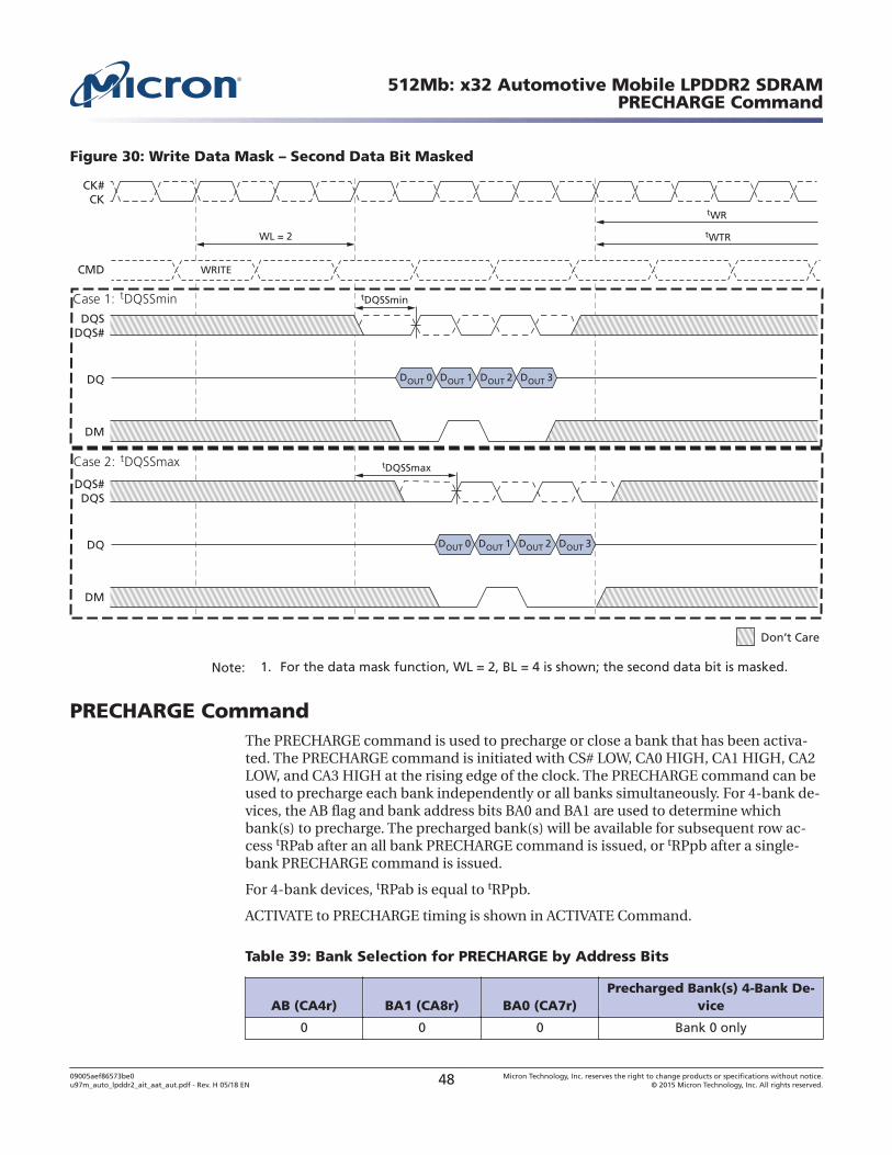
Figure 30: Write Data Mask – Second Data Bit Masked
DQSDQS#
CK#CK
DQ
Don’t Care
DM
CMD
WL = 2
tDQSSmax
tDQSSmin
DOUT 0 DOUT 1 DOUT 2 DOUT 3
WRITE
tWTR
tWR
DQS#DQS
DQ
DM
DOUT 0 DOUT 1 DOUT 2 DOUT 3
Case 1: tDQSSmin
Case 2: tDQSSmax
Note: 1. For the data mask function, WL = 2, BL = 4 is shown; the second data bit is masked.
PRECHARGE CommandThe PRECHARGE command is used to precharge or close a bank that has been activa-ted. The PRECHARGE command is initiated with CS# LOW, CA0 HIGH, CA1 HIGH, CA2LOW, and CA3 HIGH at the rising edge of the clock. The PRECHARGE command can beused to precharge each bank independently or all banks simultaneously. For 4-bank de-vices, the AB flag and bank address bits BA0 and BA1 are used to determine whichbank(s) to precharge. The precharged bank(s) will be available for subsequent row ac-cess tRPab after an all bank PRECHARGE command is issued, or tRPpb after a single-bank PRECHARGE command is issued.
For 4-bank devices, tRPab is equal to tRPpb.
ACTIVATE to PRECHARGE timing is shown in ACTIVATE Command.
Table 39: Bank Selection for PRECHARGE by Address Bits
AB (CA4r) BA1 (CA8r) BA0 (CA7r)Precharged Bank(s) 4-Bank De-
vice
0 0 0 Bank 0 only
512Mb: x32 Automotive Mobile LPDDR2 SDRAMPRECHARGE Command
09005aef86573be0u97m_auto_lpddr2_ait_aat_aut.pdf - Rev. H 05/18 EN 48 Micron Technology, Inc. reserves the right to change products or specifications without notice.
© 2015 Micron Technology, Inc. All rights reserved.
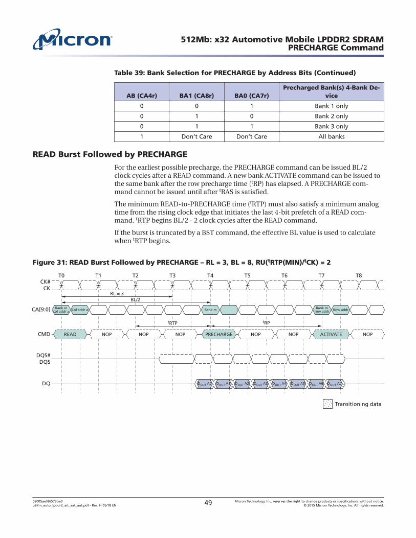
Table 39: Bank Selection for PRECHARGE by Address Bits (Continued)
AB (CA4r) BA1 (CA8r) BA0 (CA7r)Precharged Bank(s) 4-Bank De-
vice
0 0 1 Bank 1 only
0 1 0 Bank 2 only
0 1 1 Bank 3 only
1 Don’t Care Don’t Care All banks
READ Burst Followed by PRECHARGE
For the earliest possible precharge, the PRECHARGE command can be issued BL/2clock cycles after a READ command. A new bank ACTIVATE command can be issued tothe same bank after the row precharge time (tRP) has elapsed. A PRECHARGE com-mand cannot be issued until after tRAS is satisfied.
The minimum READ-to-PRECHARGE time (tRTP) must also satisfy a minimum analogtime from the rising clock edge that initiates the last 4-bit prefetch of a READ com-mand. tRTP begins BL/2 - 2 clock cycles after the READ command.
If the burst is truncated by a BST command, the effective BL value is used to calculatewhen tRTP begins.
Figure 31: READ Burst Followed by PRECHARGE – RL = 3, BL = 8, RU(tRTP(MIN)/tCK) = 2
Bank mcol addr a Col addr a
READ NOP
T0 T1 T2 T3 T4 T5 T6 T7 T8CK#
CK
CA[9:0]
CMD
DQS#DQS
DQ
RL = 3
tRP
Transitioning data
NOP NOP PRECHARGE NOP
tRTP
NOP
DOUT A4 DOUT A5 DOUT A6 DOUT A7DOUT A0 DOUT A1 DOUT A2 DOUT A3
ACTIVATE NOP
Bank m Bank mrow addr Row addr
BL/2
512Mb: x32 Automotive Mobile LPDDR2 SDRAMPRECHARGE Command
09005aef86573be0u97m_auto_lpddr2_ait_aat_aut.pdf - Rev. H 05/18 EN 49 Micron Technology, Inc. reserves the right to change products or specifications without notice.
© 2015 Micron Technology, Inc. All rights reserved.
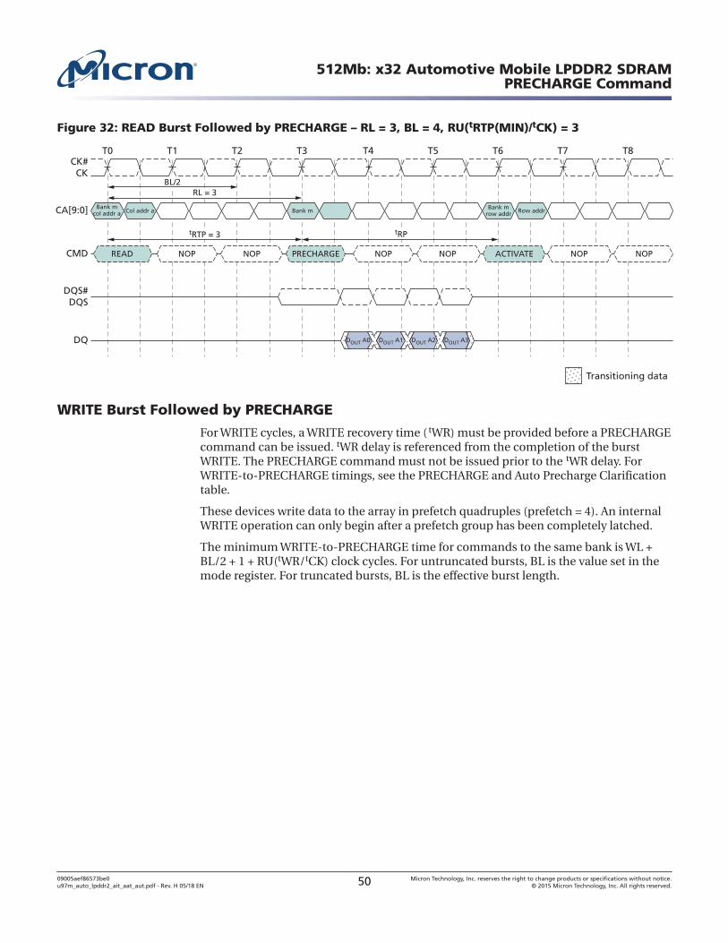
Figure 32: READ Burst Followed by PRECHARGE – RL = 3, BL = 4, RU(tRTP(MIN)/tCK) = 3
Bank mcol addr a Col addr a
READ NOP
T0 T1 T2 T3 T4 T5 T6 T7 T8CK#
CK
CA[9:0]
CMD
DQS#DQS
DQ
RL = 3
tRP
Transitioning data
NOP PRECHARGE NOPNOP
tRTP = 3
BL/2
ACTIVATE
DOUT A0 DOUT A1 DOUT A2 DOUT A3
NOP NOP
Bank m Bank mrow addr Row addr
WRITE Burst Followed by PRECHARGE
For WRITE cycles, a WRITE recovery time ( tWR) must be provided before a PRECHARGEcommand can be issued. tWR delay is referenced from the completion of the burstWRITE. The PRECHARGE command must not be issued prior to the tWR delay. ForWRITE-to-PRECHARGE timings, see the PRECHARGE and Auto Precharge Clarificationtable.
These devices write data to the array in prefetch quadruples (prefetch = 4). An internalWRITE operation can only begin after a prefetch group has been completely latched.
The minimum WRITE-to-PRECHARGE time for commands to the same bank is WL +BL/2 + 1 + RU(tWR/tCK) clock cycles. For untruncated bursts, BL is the value set in themode register. For truncated bursts, BL is the effective burst length.
512Mb: x32 Automotive Mobile LPDDR2 SDRAMPRECHARGE Command
09005aef86573be0u97m_auto_lpddr2_ait_aat_aut.pdf - Rev. H 05/18 EN 50 Micron Technology, Inc. reserves the right to change products or specifications without notice.
© 2015 Micron Technology, Inc. All rights reserved.
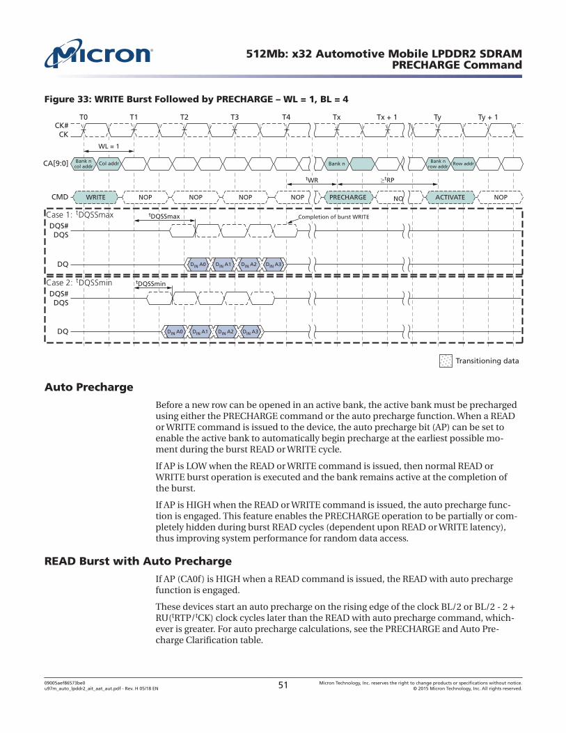
Figure 33: WRITE Burst Followed by PRECHARGE – WL = 1, BL = 4
Bank ncol addr Col addr
WRITE NOP
T0 T1 T2 T3 T4 Tx Tx + 1 Ty Ty + 1CK#
CK
CA[9:0]
CMD
DQS#DQS
DQ
WL = 1
tWR
Completion of burst WRITE
Transitioning data
NOP NOP NOP PRECHARGE
tDQSSmax
NOP
DIN A0 DIN A1 DIN A2 DIN A3
ACTIVATE NOP
Bank n Bank nrow addr
Row addr
DQS#DQS
DQ
tDQSSmin
tRP
DIN A0 DIN A1 DIN A2 DIN A3
Case 1: tDQSSmax
Case 2: tDQSSmin
Auto Precharge
Before a new row can be opened in an active bank, the active bank must be prechargedusing either the PRECHARGE command or the auto precharge function. When a READor WRITE command is issued to the device, the auto precharge bit (AP) can be set toenable the active bank to automatically begin precharge at the earliest possible mo-ment during the burst READ or WRITE cycle.
If AP is LOW when the READ or WRITE command is issued, then normal READ orWRITE burst operation is executed and the bank remains active at the completion ofthe burst.
If AP is HIGH when the READ or WRITE command is issued, the auto precharge func-tion is engaged. This feature enables the PRECHARGE operation to be partially or com-pletely hidden during burst READ cycles (dependent upon READ or WRITE latency),thus improving system performance for random data access.
READ Burst with Auto Precharge
If AP (CA0f) is HIGH when a READ command is issued, the READ with auto prechargefunction is engaged.
These devices start an auto precharge on the rising edge of the clock BL/2 or BL/2 - 2 +RU(tRTP/tCK) clock cycles later than the READ with auto precharge command, which-ever is greater. For auto precharge calculations, see the PRECHARGE and Auto Pre-charge Clarification table.
512Mb: x32 Automotive Mobile LPDDR2 SDRAMPRECHARGE Command
09005aef86573be0u97m_auto_lpddr2_ait_aat_aut.pdf - Rev. H 05/18 EN 51 Micron Technology, Inc. reserves the right to change products or specifications without notice.
© 2015 Micron Technology, Inc. All rights reserved.
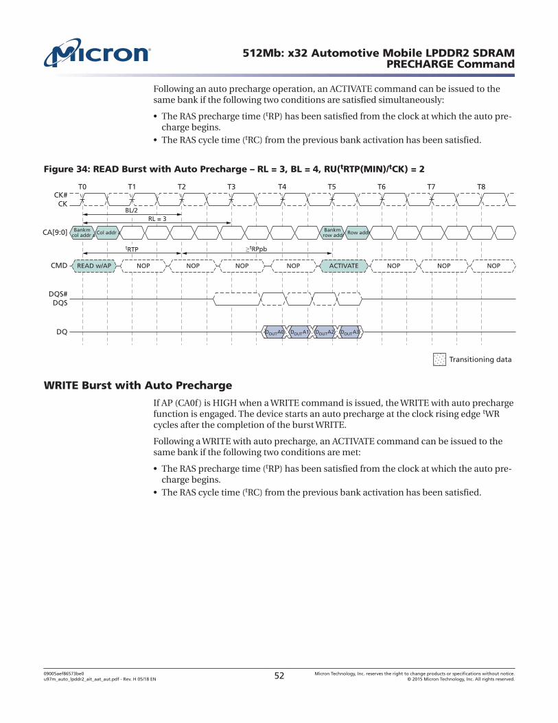
Following an auto precharge operation, an ACTIVATE command can be issued to thesame bank if the following two conditions are satisfied simultaneously:
• The RAS precharge time (tRP) has been satisfied from the clock at which the auto pre-charge begins.
• The RAS cycle time (tRC) from the previous bank activation has been satisfied.
Figure 34: READ Burst with Auto Precharge – RL = 3, BL = 4, RU(tRTP(MIN)/tCK) = 2
Bank mcol addr a Col addr a
READ w/AP NOP
T0 T1 T2 T3 T4 T5 T6 T7 T8CK#
CK
CA[9:0]
CMD
DQS#DQS
DQ
RL = 3
Transitioning data
NOP NOP NOP ACTIVATE
tRTP
BL/2
NOP
DOUT A0 DOUT A1 DOUT A2 DOUT A3
NOP NOP
Bank mrow addr Row addr
tRPpb
WRITE Burst with Auto Precharge
If AP (CA0f) is HIGH when a WRITE command is issued, the WRITE with auto prechargefunction is engaged. The device starts an auto precharge at the clock rising edge tWRcycles after the completion of the burst WRITE.
Following a WRITE with auto precharge, an ACTIVATE command can be issued to thesame bank if the following two conditions are met:
• The RAS precharge time (tRP) has been satisfied from the clock at which the auto pre-charge begins.
• The RAS cycle time (tRC) from the previous bank activation has been satisfied.
512Mb: x32 Automotive Mobile LPDDR2 SDRAMPRECHARGE Command
09005aef86573be0u97m_auto_lpddr2_ait_aat_aut.pdf - Rev. H 05/18 EN 52 Micron Technology, Inc. reserves the right to change products or specifications without notice.
© 2015 Micron Technology, Inc. All rights reserved.
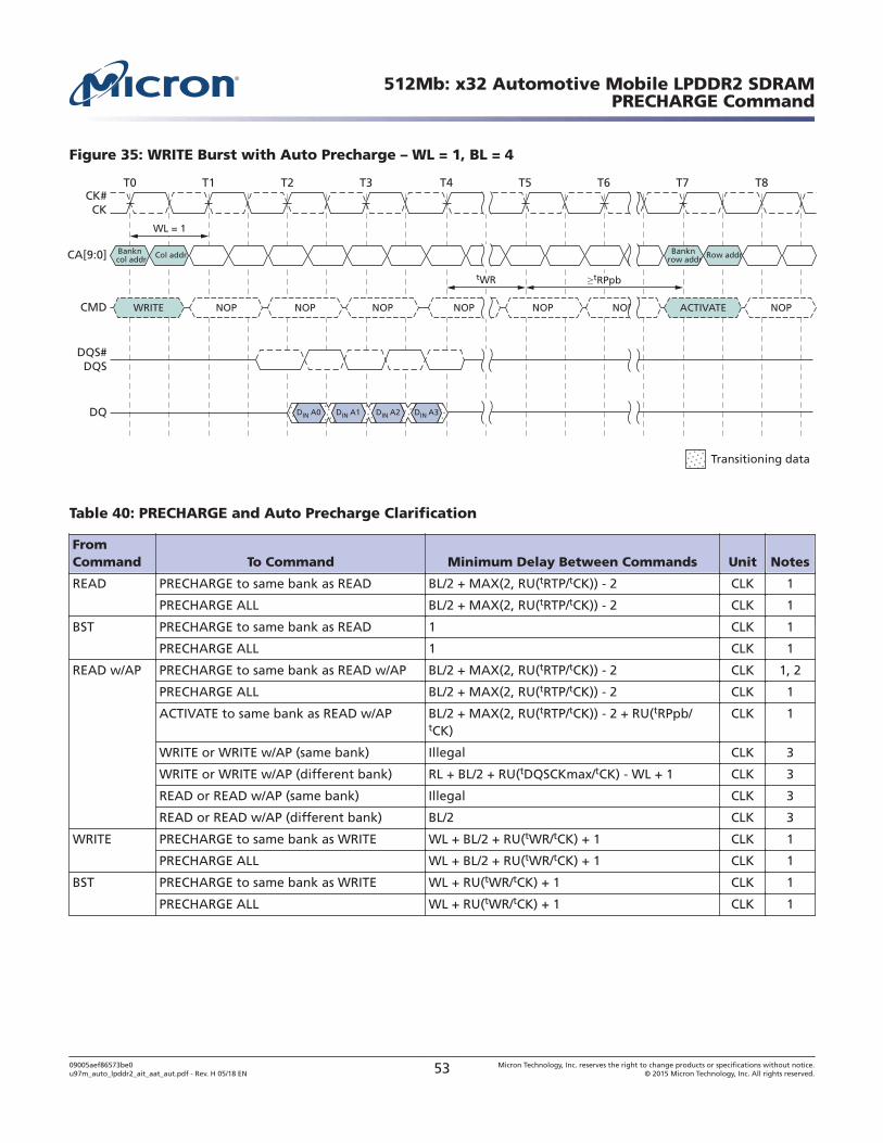
Figure 35: WRITE Burst with Auto Precharge – WL = 1, BL = 4
Bank ncol addr Col addr
WRITE NOP
T0 T1 T2 T3 T4 T5 T6 T7 T8CK#
CK
CA[9:0]
CMD
DQS#DQS
DQ
WL = 1
tWR
Transitioning data
NOP NOP NOP NOP NOP
DIN A0 DIN A1 DIN A2 DIN A3
ACTIVATE NOP
Bank nrow addr Row addr
tRPpb
Table 40: PRECHARGE and Auto Precharge Clarification
FromCommand To Command Minimum Delay Between Commands Unit Notes
READ PRECHARGE to same bank as READ BL/2 + MAX(2, RU(tRTP/tCK)) - 2 CLK 1
PRECHARGE ALL BL/2 + MAX(2, RU(tRTP/tCK)) - 2 CLK 1
BST PRECHARGE to same bank as READ 1 CLK 1
PRECHARGE ALL 1 CLK 1
READ w/AP PRECHARGE to same bank as READ w/AP BL/2 + MAX(2, RU(tRTP/tCK)) - 2 CLK 1, 2
PRECHARGE ALL BL/2 + MAX(2, RU(tRTP/tCK)) - 2 CLK 1
ACTIVATE to same bank as READ w/AP BL/2 + MAX(2, RU(tRTP/tCK)) - 2 + RU(tRPpb/tCK)
CLK 1
WRITE or WRITE w/AP (same bank) Illegal CLK 3
WRITE or WRITE w/AP (different bank) RL + BL/2 + RU(tDQSCKmax/tCK) - WL + 1 CLK 3
READ or READ w/AP (same bank) Illegal CLK 3
READ or READ w/AP (different bank) BL/2 CLK 3
WRITE PRECHARGE to same bank as WRITE WL + BL/2 + RU(tWR/tCK) + 1 CLK 1
PRECHARGE ALL WL + BL/2 + RU(tWR/tCK) + 1 CLK 1
BST PRECHARGE to same bank as WRITE WL + RU(tWR/tCK) + 1 CLK 1
PRECHARGE ALL WL + RU(tWR/tCK) + 1 CLK 1
512Mb: x32 Automotive Mobile LPDDR2 SDRAMPRECHARGE Command
09005aef86573be0u97m_auto_lpddr2_ait_aat_aut.pdf - Rev. H 05/18 EN 53 Micron Technology, Inc. reserves the right to change products or specifications without notice.
© 2015 Micron Technology, Inc. All rights reserved.
Table 40: PRECHARGE and Auto Precharge Clarification (Continued)
FromCommand To Command Minimum Delay Between Commands Unit Notes
WRITE w/AP PRECHARGE to same bank as WRITE w/AP WL + BL/2 + RU(tWR/tCK) + 1 CLK 1, 2
PRECHARGE ALL WL + BL/2 + RU(tWR/tCK) + 1 CLK 1
ACTIVATE to same bank as WRITE w/AP WL + BL/2 + RU(tWR/tCK) + 1 + RU(tRPpb/tCK) CLK 1
WRITE or WRITE w/AP (same bank) Illegal CLK 3
WRITE or WRITE w/AP (different bank) BL/2 CLK 3
READ or READ w/AP (same bank) Illegal CLK 3
READ or READ w/AP (different bank) WL + BL/2 + RU(tWTR/tCK) + 1 CLK 3
PRECHARGE PRECHARGE to same bank as PRECHARGE 1 CLK 1
PRECHARGE ALL 1 CLK 1
PRECHARGEALL
PRECHARGE 1 CLK 1
PRECHARGE ALL 1 CLK 1
Notes: 1. For a given bank, the PRECHARGE period should be counted from the latest PRECHARGEcommand—either a one-bank PRECHARGE or PRECHARGE ALL—issued to that bank.The PRECHARGE period is satisfied after tRP, depending on the latest PRECHARGE com-mand issued to that bank.
2. Any command issued during the specified minimum delay time is illegal.3. After READ with auto precharge, seamless READ operations to different banks are sup-
ported. After WRITE with auto precharge, seamless WRITE operations to different banksare supported. READ with auto precharge and WRITE with auto precharge must not beinterrupted or truncated.
SELF REFRESH OperationThe SELF REFRESH command can be used to retain data in the array, even if the rest ofthe system is powered down. When in the self refresh mode, the device retains datawithout external clocking. The device has a built-in timer to accommodate SELF RE-FRESH operation. The SELF REFRESH command is executed by taking CKE LOW, CS#LOW, CA0 LOW, CA1 LOW, and CA2 HIGH at the rising edge of the clock.
CKE must be HIGH during the clock cycle preceding a SELF REFRESH command. ANOP command must be driven in the clock cycle following the SELF REFRESH com-mand. After the power-down command is registered, CKE must be held LOW to keepthe device in self refresh mode.
Mobile LPDDR2 devices can operate in self refresh mode in both the standard and ex-tended temperature ranges. These devices also manage self refresh power consumptionwhen the operating temperature changes, resulting in the lowest possible power con-sumption across the operating temperature range. See Table 57 (page 90) for details.
After the device has entered self refresh mode, all external signals other than CKE are“Don’t Care.” For proper self refresh operation, power supply pins (VDD1, VDD2, VDDQ,and VDDCA) must be at valid levels. VDDQ can be turned off during self refresh. If VDDQ isturned off, VREFDQ must also be turned off. Prior to exiting self refresh, both VDDQ andVREFDQ must be within their respective minimum/maximum operating ranges (see theSingle-Ended AC and DC Input Levels for DQ and DM table). VREFDQ can be at any level
512Mb: x32 Automotive Mobile LPDDR2 SDRAMSELF REFRESH Operation
09005aef86573be0u97m_auto_lpddr2_ait_aat_aut.pdf - Rev. H 05/18 EN 54 Micron Technology, Inc. reserves the right to change products or specifications without notice.
© 2015 Micron Technology, Inc. All rights reserved.
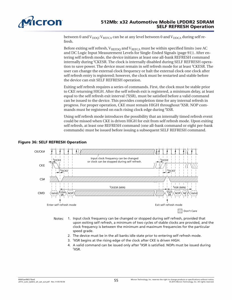
between 0 and VDDQ; VREFCA can be at any level between 0 and VDDCA during self re-fresh.
Before exiting self refresh, VREFDQ and VREFCA must be within specified limits (see ACand DC Logic Input Measurement Levels for Single-Ended Signals (page 91)). After en-tering self refresh mode, the device initiates at least one all-bank REFRESH commandinternally during tCKESR. The clock is internally disabled during SELF REFRESH opera-tion to save power. The device must remain in self refresh mode for at least tCKESR. Theuser can change the external clock frequency or halt the external clock one clock afterself refresh entry is registered; however, the clock must be restarted and stable beforethe device can exit SELF REFRESH operation.
Exiting self refresh requires a series of commands. First, the clock must be stable priorto CKE returning HIGH. After the self refresh exit is registered, a minimum delay, at leastequal to the self refresh exit interval (tXSR), must be satisfied before a valid commandcan be issued to the device. This provides completion time for any internal refresh inprogress. For proper operation, CKE must remain HIGH throughout tXSR. NOP com-mands must be registered on each rising clock edge during tXSR.
Using self refresh mode introduces the possibility that an internally timed refresh eventcould be missed when CKE is driven HIGH for exit from self refresh mode. Upon exitingself refresh, at least one REFRESH command (one all-bank command or eight per-bankcommands) must be issued before issuing a subsequent SELF REFRESH command.
Figure 36: SELF REFRESH Operation
ExitSR ValidNOPNOPEnter
SR NOP
Enter self refresh mode
Input clock frequency can be changedor clock can be stopped during self refresh.
Valid
CK/CK#
CKE
CS#
CMD
tCKESR (MIN) tXSR (MIN)
tIHCKE tIHCKE
tISCKE tISCKE
Exit self refresh mode
Don’t Care
Notes: 1. Input clock frequency can be changed or stopped during self refresh, provided thatupon exiting self refresh, a minimum of two cycles of stable clocks are provided, and theclock frequency is between the minimum and maximum frequencies for the particularspeed grade.
2. The device must be in the all banks idle state prior to entering self refresh mode.3. tXSR begins at the rising edge of the clock after CKE is driven HIGH.4. A valid command can be issued only after tXSR is satisfied. NOPs must be issued during
tXSR.
512Mb: x32 Automotive Mobile LPDDR2 SDRAMSELF REFRESH Operation
09005aef86573be0u97m_auto_lpddr2_ait_aat_aut.pdf - Rev. H 05/18 EN 55 Micron Technology, Inc. reserves the right to change products or specifications without notice.
© 2015 Micron Technology, Inc. All rights reserved.
Partial-Array Self Refresh – Bank Masking
Devices in densities of 64Mb–512Mb are comprised of four banks; densities of 1Gb andhigher are comprised of eight banks. Each bank can be configured independentlywhether or not a SELF REFRESH operation will occur in that bank. One 8-bit mode reg-ister (accessible via the MRW command) is assigned to program the bank-masking sta-tus of each bank up to eight banks. For bank masking bit assignments, see the MR16PASR Bank Mask (MA[7:0] = 010h) and MR16 Op-Code Bit Definitions tables.
The mask bit to the bank enables or disables a refresh operation of the entire memoryspace within the bank. If a bank is masked using the bank mask register, a REFRESH op-eration to the entire bank is blocked and bank data retention is not guaranteed in selfrefresh mode. To enable a REFRESH operation to a bank, the corresponding bank maskbit must be programmed as “unmasked.” When a bank mask bit is unmasked, the arrayspace being refreshed within that bank is determined by the programmed status of thesegment mask bits.
512Mb: x32 Automotive Mobile LPDDR2 SDRAMSELF REFRESH Operation
09005aef86573be0u97m_auto_lpddr2_ait_aat_aut.pdf - Rev. H 05/18 EN 56 Micron Technology, Inc. reserves the right to change products or specifications without notice.
© 2015 Micron Technology, Inc. All rights reserved.
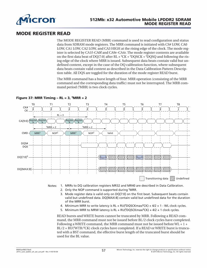
MODE REGISTER READThe MODE REGISTER READ (MRR) command is used to read configuration and statusdata from SDRAM mode registers. The MRR command is initiated with CS# LOW, CA0LOW, CA1 LOW, CA2 LOW, and CA3 HIGH at the rising edge of the clock. The mode reg-ister is selected by CA1f–CA0f and CA9r–CA4r. The mode register contents are availableon the first data beat of DQ[7:0] after RL × tCK + tDQSCK + tDQSQ and following the ris-ing edge of the clock where MRR is issued. Subsequent data beats contain valid but un-defined content, except in the case of the DQ calibration function, where subsequentdata beats contain valid content as described in the Data Calibration Pattern Descrip-tion table. All DQS are toggled for the duration of the mode register READ burst.
The MRR command has a burst length of four. MRR operation (consisting of the MRRcommand and the corresponding data traffic) must not be interrupted. The MRR com-mand period (tMRR) is two clock cycles.
Figure 37: MRR Timing – RL = 3, tMRR = 2
RegisterA
RegisterA
MRR1 NOP2 NOP2
T0 T1 T2 T3 T4 T5 T6 T7 T8CK#
CK
CA[9:0]
CMD
DQS#DQS
DQ[7:0]3
RL = 3
MRR1 Valid
tMRR = 2 tMRR = 2
DQ[MAX:8]
RegisterB
RegisterB
DOUT BDOUT A
Transitioning data Undefined
Notes: 1. MRRs to DQ calibration registers MR32 and MR40 are described in Data Calibration.2. Only the NOP command is supported during tMRR.3. Mode register data is valid only on DQ[7:0] on the first beat. Subsequent beats contain
valid but undefined data. DQ[MAX:8] contain valid but undefined data for the durationof the MRR burst.
4. Minimum MRR to write latency is RL + RU(tDQSCKmax/tCK) + 4/2 + 1 - WL clock cycles.5. Minimum MRR to MRW latency is RL + RU(tDQSCKmax/tCK) + 4/2 + 1 clock cycles.
READ bursts and WRITE bursts cannot be truncated by MRR. Following a READ com-mand, the MRR command must not be issued before BL/2 clock cycles have completed.Following a WRITE command, the MRR command must not be issued before WL + 1 +BL/2 + RU(tWTR/tCK) clock cycles have completed. If a READ or WRITE burst is trunca-ted with a BST command, the effective burst length of the truncated burst should beused for the BL value.
512Mb: x32 Automotive Mobile LPDDR2 SDRAMMODE REGISTER READ
09005aef86573be0u97m_auto_lpddr2_ait_aat_aut.pdf - Rev. H 05/18 EN 57 Micron Technology, Inc. reserves the right to change products or specifications without notice.
© 2015 Micron Technology, Inc. All rights reserved.
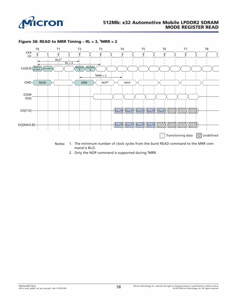
Figure 38: READ to MRR Timing – RL = 3, tMRR = 2
Bank mcol addr a Col addr a
READ NOP2
T0 T1 T2 T3 T4 T5 T6 T7 T8CK#CK
CA[9:0]
CMD
DQS#DQS
DQ[7:0]
DQ[MAX:8]
RL = 3
Transitioning data Undefined
tMRR = 2
BL/21
DOUT BDOUT A0 DOUT A1 DOUT A2 DOUT A3
DOUT A0 DOUT A1 DOUT A2 DOUT A3
Valid
RegisterB
RegisterB
MRR
Notes: 1. The minimum number of clock cycles from the burst READ command to the MRR com-mand is BL/2.
2. Only the NOP command is supported during tMRR.
512Mb: x32 Automotive Mobile LPDDR2 SDRAMMODE REGISTER READ
09005aef86573be0u97m_auto_lpddr2_ait_aat_aut.pdf - Rev. H 05/18 EN 58 Micron Technology, Inc. reserves the right to change products or specifications without notice.
© 2015 Micron Technology, Inc. All rights reserved.
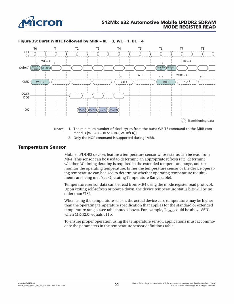
Figure 39: Burst WRITE Followed by MRR – RL = 3, WL = 1, BL = 4
Bank ncol addr a Col addr a
WRITE
T0 T1 T2 T3 T4 T5 T6 T7 T8CK#CK
CA[9:0]
CMD
DQS#DQS
DQ
WL = 3
tWTR
Transitioning data
tMRR = 2
RL = 3
DIN A0 DIN A1 DIN A2 DIN A3
Valid
RegisterB
RegisterB
MRR1 NOP2
Notes: 1. The minimum number of clock cycles from the burst WRITE command to the MRR com-mand is [WL + 1 + BL/2 + RU(tWTR/tCK)].
2. Only the NOP command is supported during tMRR.
Temperature Sensor
Mobile LPDDR2 devices feature a temperature sensor whose status can be read fromMR4. This sensor can be used to determine an appropriate refresh rate, determinewhether AC timing derating is required in the extended temperature range, and/ormonitor the operating temperature. Either the temperature sensor or the device operat-ing temperature can be used to determine whether operating temperature require-ments are being met (see Operating Temperature Range table).
Temperature sensor data can be read from MR4 using the mode register read protocol.Upon exiting self-refresh or power-down, the device temperature status bits will be noolder than tTSI.
When using the temperature sensor, the actual device case temperature may be higherthan the operating temperature specification that applies for the standard or extendedtemperature ranges (see table noted above). For example, TCASE could be above 85˚Cwhen MR4[2:0] equals 011b.
To ensure proper operation using the temperature sensor, applications must accommo-date the parameters in the temperature sensor definitions table.
512Mb: x32 Automotive Mobile LPDDR2 SDRAMMODE REGISTER READ
09005aef86573be0u97m_auto_lpddr2_ait_aat_aut.pdf - Rev. H 05/18 EN 59 Micron Technology, Inc. reserves the right to change products or specifications without notice.
© 2015 Micron Technology, Inc. All rights reserved.
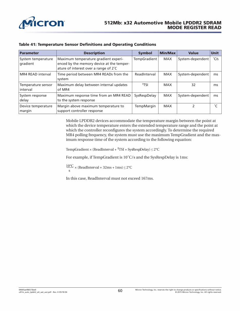
Table 41: Temperature Sensor Definitions and Operating Conditions
Parameter Description Symbol Min/Max Value Unit
System temperaturegradient
Maximum temperature gradient experi-enced by the memory device at the temper-ature of interest over a range of 2˚C
TempGradient MAX System-dependent ˚C/s
MR4 READ interval Time period between MR4 READs from thesystem
ReadInterval MAX System-dependent ms
Temperature sensorinterval
Maximum delay between internal updatesof MR4
tTSI MAX 32 ms
System responsedelay
Maximum response time from an MR4 READto the system response
SysRespDelay MAX System-dependent ms
Device temperaturemargin
Margin above maximum temperature tosupport controller response
TempMargin MAX 2 ˚C
Mobile LPDDR2 devices accommodate the temperature margin between the point atwhich the device temperature enters the extended temperature range and the point atwhich the controller reconfigures the system accordingly. To determine the requiredMR4 polling frequency, the system must use the maximum TempGradient and the max-imum response time of the system according to the following equation:
TempGradient × (ReadInterval + tTSI + SysRespDelay) 2°C
For example, if TempGradient is 10˚C/s and the SysRespDelay is 1ms:
10°Cs
× (ReadInterval + 32ms + 1ms) 2°C
In this case, ReadInterval must not exceed 167ms.
512Mb: x32 Automotive Mobile LPDDR2 SDRAMMODE REGISTER READ
09005aef86573be0u97m_auto_lpddr2_ait_aat_aut.pdf - Rev. H 05/18 EN 60 Micron Technology, Inc. reserves the right to change products or specifications without notice.
© 2015 Micron Technology, Inc. All rights reserved.
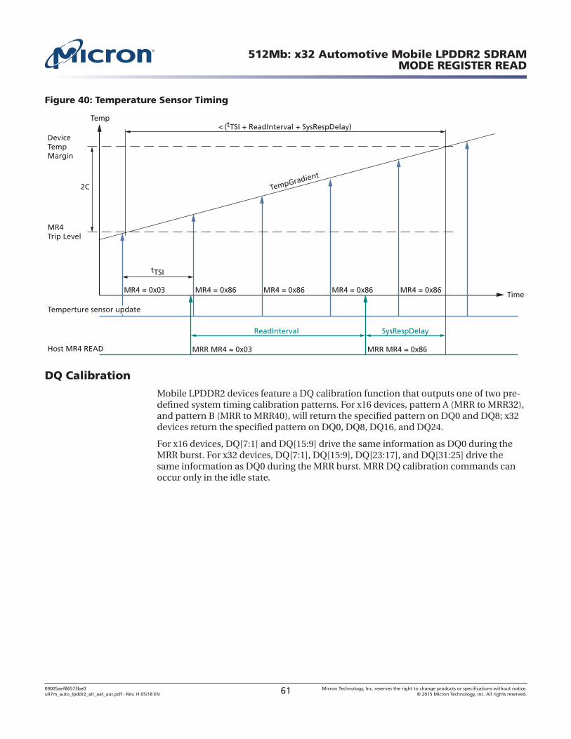
Figure 40: Temperature Sensor Timing
Host MR4 READ
DeviceTempMargin
MR4Trip Level
2C
MR4 = 0x03
MRR MR4 = 0x03 MRR MR4 = 0x86
tTSI
< (tTSI + ReadInterval + SysRespDelay)
ReadInterval SysRespDelay
MR4 = 0x86 MR4 = 0x86 MR4 = 0x86 MR4 = 0x86Time
Temp
TempGradient
Temperture sensor update
DQ Calibration
Mobile LPDDR2 devices feature a DQ calibration function that outputs one of two pre-defined system timing calibration patterns. For x16 devices, pattern A (MRR to MRR32),and pattern B (MRR to MRR40), will return the specified pattern on DQ0 and DQ8; x32devices return the specified pattern on DQ0, DQ8, DQ16, and DQ24.
For x16 devices, DQ[7:1] and DQ[15:9] drive the same information as DQ0 during theMRR burst. For x32 devices, DQ[7:1], DQ[15:9], DQ[23:17], and DQ[31:25] drive thesame information as DQ0 during the MRR burst. MRR DQ calibration commands canoccur only in the idle state.
512Mb: x32 Automotive Mobile LPDDR2 SDRAMMODE REGISTER READ
09005aef86573be0u97m_auto_lpddr2_ait_aat_aut.pdf - Rev. H 05/18 EN 61 Micron Technology, Inc. reserves the right to change products or specifications without notice.
© 2015 Micron Technology, Inc. All rights reserved.
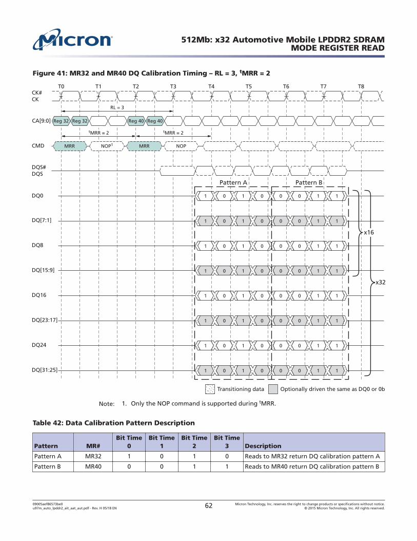
Figure 41: MR32 and MR40 DQ Calibration Timing – RL = 3, tMRR = 2
MRR NOP1 NOP
T0 T1 T2 T3 T4 T5 T6 T7 T8CK#CK
CA[9:0]
CMD
DQS#DQS
DQ0
DQ[7:1]
DQ8
DQ[15:9]
DQ16
DQ[23:17]
DQ24
DQ[31:25]
RL = 3
Transitioning data Optionally driven the same as DQ0 or 0b
tMRR = 2tMRR = 2
0 0 1 11 0 1 0
Reg 40Reg 40Reg 32Reg 32
MRR
0 0 1 11 0 1 0
0 0 1 11 0 1 0
0 0 1 11 0 1 0
0 0 1 11 0 1 0
0 0 1 11 0 1 0
0 0 1 11 0 1 0
0 0 1 11 0 1 0
Pattern A Pattern B
x32
x16
Note: 1. Only the NOP command is supported during tMRR.
Table 42: Data Calibration Pattern Description
Pattern MR#Bit Time
0Bit Time
1Bit Time
2Bit Time
3 Description
Pattern A MR32 1 0 1 0 Reads to MR32 return DQ calibration pattern A
Pattern B MR40 0 0 1 1 Reads to MR40 return DQ calibration pattern B
512Mb: x32 Automotive Mobile LPDDR2 SDRAMMODE REGISTER READ
09005aef86573be0u97m_auto_lpddr2_ait_aat_aut.pdf - Rev. H 05/18 EN 62 Micron Technology, Inc. reserves the right to change products or specifications without notice.
© 2015 Micron Technology, Inc. All rights reserved.
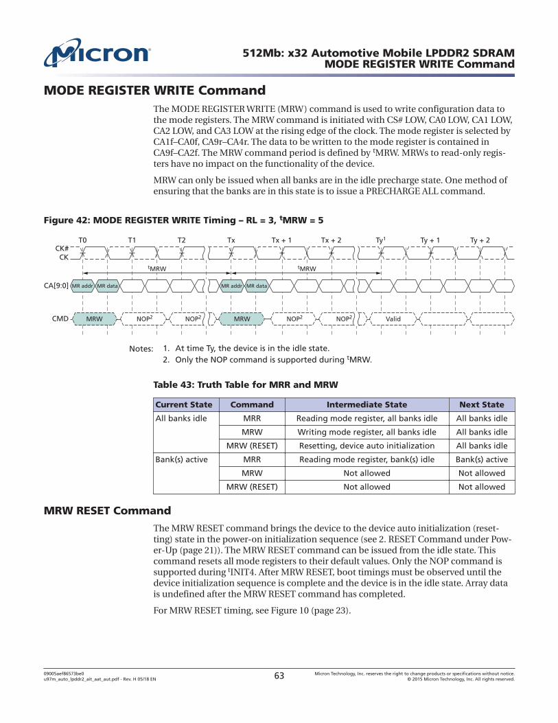
MODE REGISTER WRITE CommandThe MODE REGISTER WRITE (MRW) command is used to write configuration data tothe mode registers. The MRW command is initiated with CS# LOW, CA0 LOW, CA1 LOW,CA2 LOW, and CA3 LOW at the rising edge of the clock. The mode register is selected byCA1f–CA0f, CA9r–CA4r. The data to be written to the mode register is contained inCA9f–CA2f. The MRW command period is defined by tMRW. MRWs to read-only regis-ters have no impact on the functionality of the device.
MRW can only be issued when all banks are in the idle precharge state. One method ofensuring that the banks are in this state is to issue a PRECHARGE ALL command.
Figure 42: MODE REGISTER WRITE Timing – RL = 3, tMRW = 5
MR dataMR addr
MRW NOP2 MRW
T0 T1 T2 Tx Tx + 1 Tx + 2 Ty1 Ty + 1 Ty + 2CK#
CK
CA[9:0]
CMD Valid
tMRW tMRW
MR dataMR addr
NOP2 NOP2 NOP2
Notes: 1. At time Ty, the device is in the idle state.2. Only the NOP command is supported during tMRW.
Table 43: Truth Table for MRR and MRW
Current State Command Intermediate State Next State
All banks idle MRR Reading mode register, all banks idle All banks idle
MRW Writing mode register, all banks idle All banks idle
MRW (RESET) Resetting, device auto initialization All banks idle
Bank(s) active MRR Reading mode register, bank(s) idle Bank(s) active
MRW Not allowed Not allowed
MRW (RESET) Not allowed Not allowed
MRW RESET Command
The MRW RESET command brings the device to the device auto initialization (reset-ting) state in the power-on initialization sequence (see 2. RESET Command under Pow-er-Up (page 21)). The MRW RESET command can be issued from the idle state. Thiscommand resets all mode registers to their default values. Only the NOP command issupported during tINIT4. After MRW RESET, boot timings must be observed until thedevice initialization sequence is complete and the device is in the idle state. Array datais undefined after the MRW RESET command has completed.
For MRW RESET timing, see Figure 10 (page 23).
512Mb: x32 Automotive Mobile LPDDR2 SDRAMMODE REGISTER WRITE Command
09005aef86573be0u97m_auto_lpddr2_ait_aat_aut.pdf - Rev. H 05/18 EN 63 Micron Technology, Inc. reserves the right to change products or specifications without notice.
© 2015 Micron Technology, Inc. All rights reserved.
MRW ZQ Calibration Commands
The MRW command is used to initiate a ZQ calibration command that calibrates outputdriver impedance across process, temperature, and voltage. LPDDR2-S4 devices sup-port ZQ calibration. To achieve tighter tolerances, proper ZQ calibration must be per-formed.
There are four ZQ calibration commands and related timings: tZQINIT, tZQRESET,tZQCL, and tZQCS. tZQINIT is used for initialization calibration; tZQRESET is used forresetting ZQ to the default output impedance; tZQCL is used for long calibration(s); andtZQCS is used for short calibration(s). See the MR10 Calibration (MA[7:0] = 0Ah) tablefor ZQ calibration command code definitions.
ZQINIT must be performed for LPDDR2 devices. ZQINIT provides an output impe-dance accuracy of ±15%. After initialization, the ZQ calibration long (ZQCL) can be usedto recalibrate the system to an output impedance accuracy of ±15%. A ZQ calibrationshort (ZQCS) can be used periodically to compensate for temperature and voltage driftin the system.
ZQRESET resets the output impedance calibration to a default accuracy of ±30% acrossprocess, voltage, and temperature. This command is used to ensure output impedanceaccuracy to ±30% when ZQCS and ZQCL commands are not used.
One ZQCS command can effectively correct at least 1.5% (ZQ correction) of output im-pedance errors within tZQCS for all speed bins, assuming the maximum sensitivitiesspecified in Table 74 and Table 75 (page 106) are met. The appropriate interval betweenZQCS commands can be determined using these tables and system-specific parame-ters.
Mobile LPDDR2 devices are subject to temperature drift rate (Tdriftrate) and voltage driftrate (Vdriftrate) in various applications. To accommodate drift rates and calculate thenecessary interval between ZQCS commands, apply the following formula:
ZQcorrection
(Tsens × Tdriftrate) + (Vsens × Vdriftrate)
Where Tsens = MAX (dRONdT) and Vsens = MAX (dRONdV) define temperature and volt-age sensitivities.
For example, if Tsens = 0.75%/˚C, Vsens = 0.20%/mV, Tdriftrate = 1˚C/sec, and Vdriftrate =15 mV/sec, then the interval between ZQCS commands is calculated as:
1.5(0.75 × 1) + (0.20 × 15)
= 0.4s
A ZQ calibration command can only be issued when the device is in the idle state withall banks precharged.
No other activities can be performed on the data bus during calibration periods(tZQINIT, tZQCL, or tZQCS). The quiet time on the data bus helps to accurately calibrateoutput impedance. There is no required quiet time after the ZQRESET command. Ifmultiple devices share a single ZQ resistor, only one device can be calibrating at any giv-en time. After calibration is complete, the ZQ ball circuitry is disabled to reduce powerconsumption.
512Mb: x32 Automotive Mobile LPDDR2 SDRAMMODE REGISTER WRITE Command
09005aef86573be0u97m_auto_lpddr2_ait_aat_aut.pdf - Rev. H 05/18 EN 64 Micron Technology, Inc. reserves the right to change products or specifications without notice.
© 2015 Micron Technology, Inc. All rights reserved.
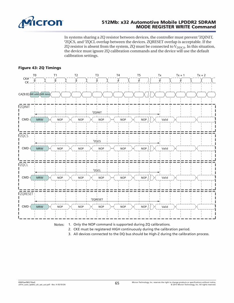
In systems sharing a ZQ resistor between devices, the controller must prevent tZQINIT,tZQCS, and tZQCL overlap between the devices. ZQRESET overlap is acceptable. If theZQ resistor is absent from the system, ZQ must be connected to VDDCA. In this situation,the device must ignore ZQ calibration commands and the device will use the defaultcalibration settings.
Figure 43: ZQ Timings
MR dataMR addr
MRW NOP
T0 T1 T2 T3 T4 T5 Tx Tx + 1 Tx + 2CK#
CK
CA[9:0]
CMD Valid
tZQINIT
NOP NOP NOP NOP
MRWCMD Valid
tZQCS
MRWCMD Valid
tZQCL
MRWCMD Valid
tZQRESET
ZQINIT
ZQCS
ZQCL
ZQRESET
NOP NOP NOP NOP NOP
NOP NOP NOP NOP NOP
NOP NOP NOP NOP NOP
Notes: 1. Only the NOP command is supported during ZQ calibrations.2. CKE must be registered HIGH continuously during the calibration period.3. All devices connected to the DQ bus should be High-Z during the calibration process.
512Mb: x32 Automotive Mobile LPDDR2 SDRAMMODE REGISTER WRITE Command
09005aef86573be0u97m_auto_lpddr2_ait_aat_aut.pdf - Rev. H 05/18 EN 65 Micron Technology, Inc. reserves the right to change products or specifications without notice.
© 2015 Micron Technology, Inc. All rights reserved.
ZQ External Resistor Value, Tolerance, and Capacitive Loading
To use the ZQ calibration function, a 240 ohm (±1% tolerance) external resistor must beconnected between the ZQ pin and ground. A single resistor can be used for each deviceor one resistor can be shared between multiple devices if the ZQ calibration timings foreach device do not overlap. The total capacitive loading on the ZQ pin must be limited(see the Input/Output Capacitance table).
Power-DownPower-down is entered synchronously when CKE is registered LOW and CS# is HIGH atthe rising edge of clock. A NOP command must be driven in the clock cycle followingpower-down entry. CKE must not go LOW while MRR, MRW, READ, or WRITE opera-tions are in progress. CKE can go LOW while any other operations such as ACTIVATE,PRECHARGE, auto precharge, or REFRESH are in progress, but the power-down IDDspecification will not be applied until such operations are complete.
If power-down occurs when all banks are idle, this mode is referred to as idle power-down; if power-down occurs when there is a row active in any bank, this mode is refer-red to as active power-down.
Entering power-down deactivates the input and output buffers, excluding CK, CK#, andCKE. In power-down mode, CKE must be held LOW; all other input signals are “Don’tCare.” CKE LOW must be maintained until tCKE is satisfied. VREFCA must be maintainedat a valid level during power-down.
VDDQ can be turned off during power-down. If VDDQ is turned off, VREFDQ must also beturned off. Prior to exiting power-down, both VDDQ and VREFDQ must be within their re-spective minimum/maximum operating ranges (see AC and DC Operating Conditions).
No refresh operations are performed in power-down mode. The maximum duration inpower-down mode is only limited by the refresh requirements outlined in REFRESHCommand.
The power-down state is exited when CKE is registered HIGH. The controller must driveCS# HIGH in conjunction with CKE HIGH when exiting the power-down state. CKEHIGH must be maintained until tCKE is satisfied. A valid, executable command can beapplied with power-down exit latency tXP after CKE goes HIGH. Power-down exit laten-cy is defined in the AC Timing section.
512Mb: x32 Automotive Mobile LPDDR2 SDRAMPower-Down
09005aef86573be0u97m_auto_lpddr2_ait_aat_aut.pdf - Rev. H 05/18 EN 66 Micron Technology, Inc. reserves the right to change products or specifications without notice.
© 2015 Micron Technology, Inc. All rights reserved.
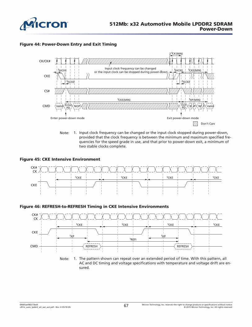
Figure 44: Power-Down Entry and Exit Timing
ExitPD ValidNOPNOPEnter
PD NOP
Enter power-down mode
Input clock frequency can be changedor the input clock can be stopped during power-down.1
Valid
CK/CK#
CKE
CS#
CMD
tCKE (MIN) tXP (MIN)
tCKE (MIN)
2 tCK (MIN)
tIHCKE tIHCKE
Exit power-down mode
Don’t Care
tISCKE tISCKE
Note: 1. Input clock frequency can be changed or the input clock stopped during power-down,provided that the clock frequency is between the minimum and maximum specified fre-quencies for the speed grade in use, and that prior to power-down exit, a minimum oftwo stable clocks complete.
Figure 45: CKE Intensive Environment
CK#CK
CKE
tCKEtCKE tCKE tCKE
Figure 46: REFRESH-to-REFRESH Timing in CKE Intensive Environments
CK#CK
CKE
CMD
tCKEtCKE tCKE tCKE
REFRESH REFRESH
tXPtREFI
tXP
Note: 1. The pattern shown can repeat over an extended period of time. With this pattern, allAC and DC timing and voltage specifications with temperature and voltage drift are en-sured.
512Mb: x32 Automotive Mobile LPDDR2 SDRAMPower-Down
09005aef86573be0u97m_auto_lpddr2_ait_aat_aut.pdf - Rev. H 05/18 EN 67 Micron Technology, Inc. reserves the right to change products or specifications without notice.
© 2015 Micron Technology, Inc. All rights reserved.
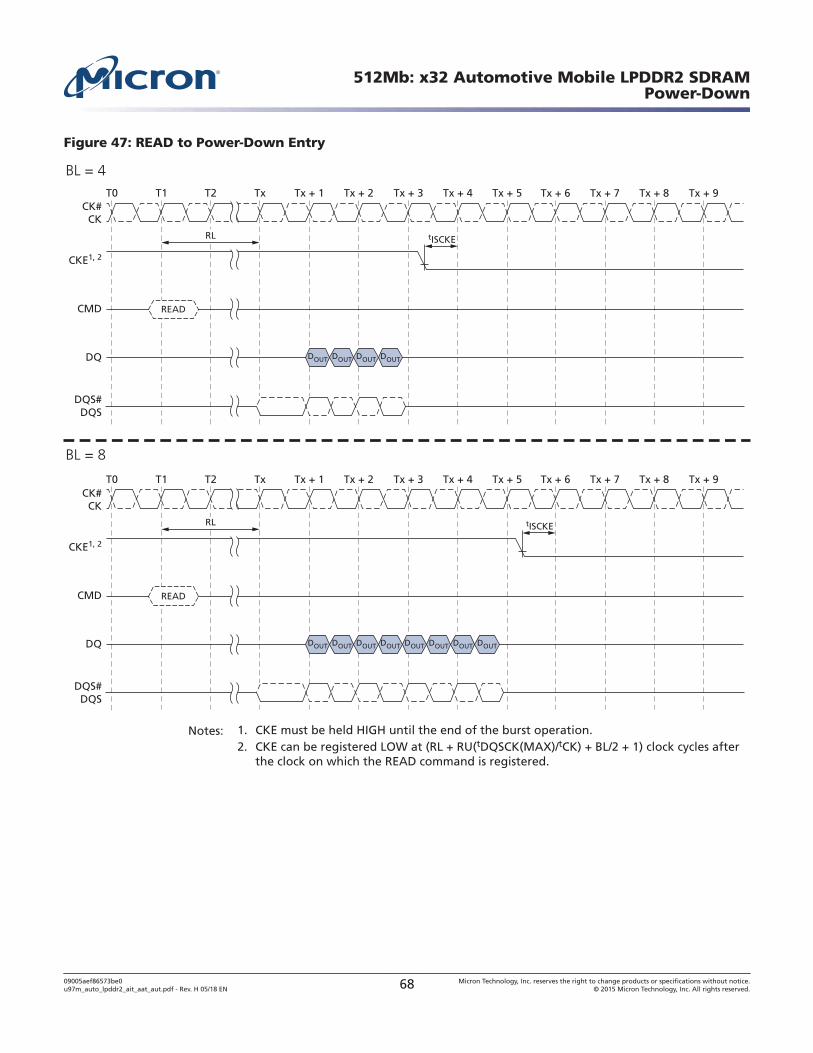
Figure 47: READ to Power-Down Entry
CK#CK
CKE1, 2
T0 T1 T2 Tx Tx + 1 Tx + 2 Tx + 3 Tx + 4 Tx + 5 Tx + 6 Tx + 7 Tx + 8 Tx + 9
CMD
DQ
DQS#DQS
READ
DOUT DOUT DOUT DOUT
RL tISCKE
CK#CK
CKE1, 2
T0 T1 T2 Tx Tx + 1 Tx + 2 Tx + 3 Tx + 4 Tx + 5 Tx + 6 Tx + 7 Tx + 8 Tx + 9
CMD
DQ
DQS#DQS
READ
DOUT DOUT DOUT DOUT DOUT DOUT DOUT DOUT
RL tISCKE
BL = 4
BL = 8
Notes: 1. CKE must be held HIGH until the end of the burst operation.2. CKE can be registered LOW at (RL + RU(tDQSCK(MAX)/tCK) + BL/2 + 1) clock cycles after
the clock on which the READ command is registered.
512Mb: x32 Automotive Mobile LPDDR2 SDRAMPower-Down
09005aef86573be0u97m_auto_lpddr2_ait_aat_aut.pdf - Rev. H 05/18 EN 68 Micron Technology, Inc. reserves the right to change products or specifications without notice.
© 2015 Micron Technology, Inc. All rights reserved.
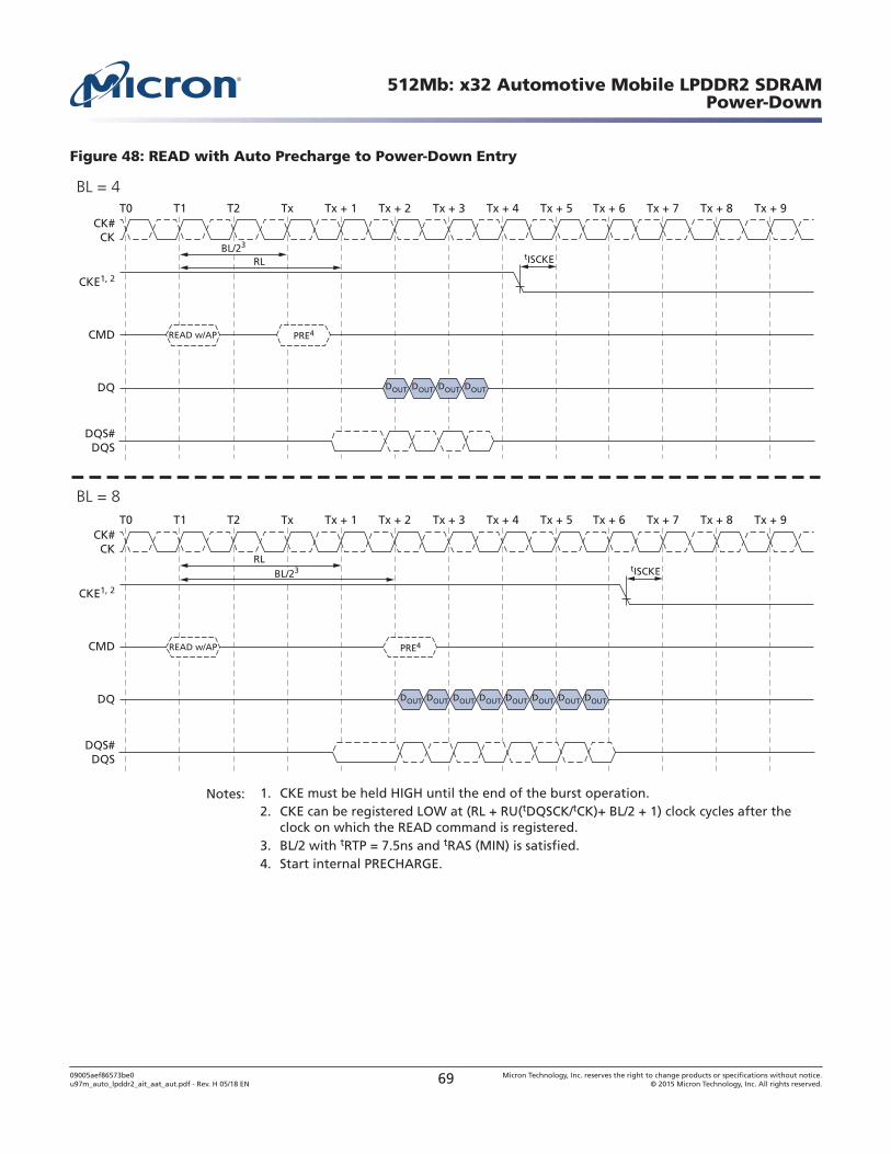
Figure 48: READ with Auto Precharge to Power-Down Entry
CK#CK
CKE1, 2
T0 T1 T2 Tx Tx + 1 Tx + 2 Tx + 3 Tx + 4 Tx + 5 Tx + 6 Tx + 7 Tx + 8 Tx + 9
CMD
DQ
DQS#DQS
READ w/AP PRE4
DOUT DOUT DOUT DOUT
RL tISCKEBL/23
READ w/AP PRE4
BL/23
CK#CK
CKE1, 2
T0 T1 T2 Tx Tx + 1 Tx + 2 Tx + 3 Tx + 4 Tx + 5 Tx + 6 Tx + 7 Tx + 8 Tx + 9
CMD
DQ
DQS#DQS
DOUT DOUT DOUT DOUT DOUT DOUT DOUT DOUT
RLtISCKE
BL = 4
BL = 8
Notes: 1. CKE must be held HIGH until the end of the burst operation.2. CKE can be registered LOW at (RL + RU(tDQSCK/tCK)+ BL/2 + 1) clock cycles after the
clock on which the READ command is registered.3. BL/2 with tRTP = 7.5ns and tRAS (MIN) is satisfied.4. Start internal PRECHARGE.
512Mb: x32 Automotive Mobile LPDDR2 SDRAMPower-Down
09005aef86573be0u97m_auto_lpddr2_ait_aat_aut.pdf - Rev. H 05/18 EN 69 Micron Technology, Inc. reserves the right to change products or specifications without notice.
© 2015 Micron Technology, Inc. All rights reserved.
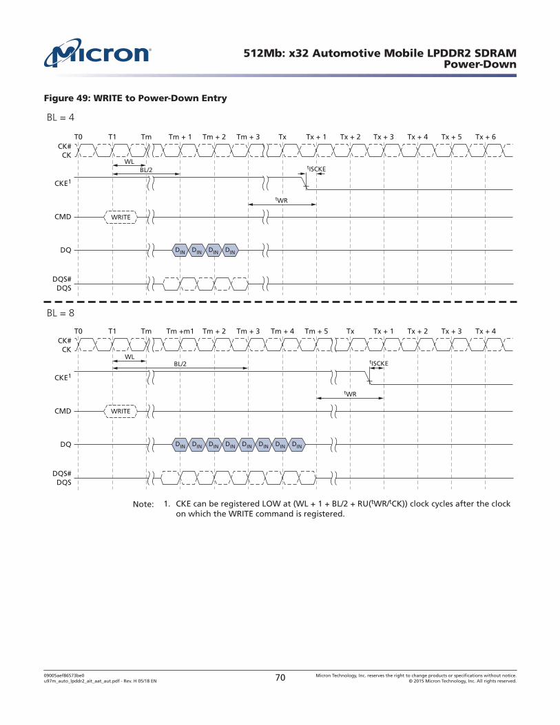
Figure 49: WRITE to Power-Down Entry
CK#CK
CKE1
T0 T1 Tm Tm + 1 Tm + 2 Tm + 3 Tx Tx + 1 Tx + 2 Tx + 3 Tx + 4 Tx + 5 Tx + 6
CMD
DQ
DQS#DQS
WRITE
DIN DIN DIN DIN
WL
tWR
tWR
CK#CK
CKE1
T0 T1 Tm Tm +m1 Tm + 2 Tm + 3 Tm + 4 Tm + 5 Tx Tx + 1 Tx + 2 Tx + 3 Tx + 4
CMD
DQ
DQS#DQS
WRITE
DIN DIN DIN DIN DIN DIN DIN DIN
WLtISCKE
BL/2
BL/2
tISCKE
BL = 4
BL = 8
Note: 1. CKE can be registered LOW at (WL + 1 + BL/2 + RU(tWR/tCK)) clock cycles after the clockon which the WRITE command is registered.
512Mb: x32 Automotive Mobile LPDDR2 SDRAMPower-Down
09005aef86573be0u97m_auto_lpddr2_ait_aat_aut.pdf - Rev. H 05/18 EN 70 Micron Technology, Inc. reserves the right to change products or specifications without notice.
© 2015 Micron Technology, Inc. All rights reserved.
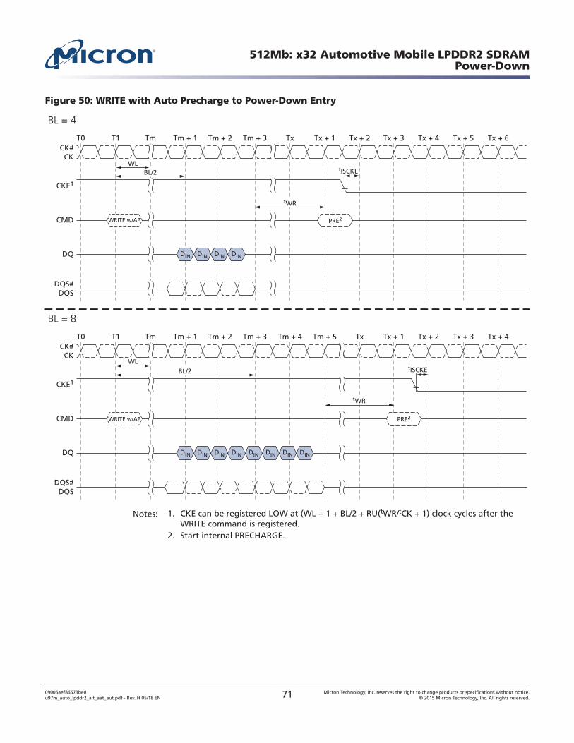
Figure 50: WRITE with Auto Precharge to Power-Down Entry
CK#CK
CKE1
T0 T1 Tm Tm + 1 Tm + 2 Tm + 3 Tx Tx + 1 Tx + 2 Tx + 3 Tx + 4 Tx + 5 Tx + 6
CMD
DQ
DQS#DQS
WRITE w/AP PRE2
DIN DIN DIN DIN
WLBL/2
BL/2
CK#CK
CKE1
T0 T1 Tm Tm + 1 Tm + 2 Tm + 3 Tm + 4 Tm + 5 Tx Tx + 1 Tx + 2 Tx + 3 Tx + 4
CMD
DQ
DQS#DQS
DIN DIN DIN DIN DIN DIN DIN DIN
WL
tISCKE
tWR
tWR
PRE2
tISCKE
BL = 4
BL = 8
WRITE w/AP
Notes: 1. CKE can be registered LOW at (WL + 1 + BL/2 + RU(tWR/tCK + 1) clock cycles after theWRITE command is registered.
2. Start internal PRECHARGE.
512Mb: x32 Automotive Mobile LPDDR2 SDRAMPower-Down
09005aef86573be0u97m_auto_lpddr2_ait_aat_aut.pdf - Rev. H 05/18 EN 71 Micron Technology, Inc. reserves the right to change products or specifications without notice.
© 2015 Micron Technology, Inc. All rights reserved.
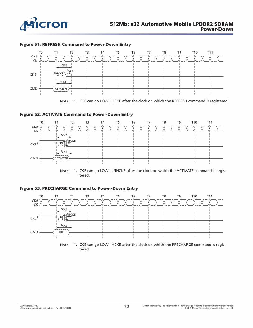
Figure 51: REFRESH Command to Power-Down Entry
CK#CK
CKE1
CMD
tCKE
REFRESH
tCKE
tIHCKEtISCKE
T0 T1 T2 T3 T4 T5 T6 T7 T8 T9 T10 T11
Note: 1. CKE can go LOW tIHCKE after the clock on which the REFRESH command is registered.
Figure 52: ACTIVATE Command to Power-Down Entry
CK#CK
CKE1
CMD
tCKE
ACTIVATE
tCKE
tIHCKEtISCKE
T0 T1 T2 T3 T4 T5 T6 T7 T8 T9 T10 T11
Note: 1. CKE can go LOW at tIHCKE after the clock on which the ACTIVATE command is regis-tered.
Figure 53: PRECHARGE Command to Power-Down Entry
CK#CK
CKE1
CMD
tCKE
PRE
tCKE
tIHCKEtISCKE
T0 T1 T2 T3 T4 T5 T6 T7 T8 T9 T10 T11
Note: 1. CKE can go LOW tIHCKE after the clock on which the PRECHARGE command is regis-tered.
512Mb: x32 Automotive Mobile LPDDR2 SDRAMPower-Down
09005aef86573be0u97m_auto_lpddr2_ait_aat_aut.pdf - Rev. H 05/18 EN 72 Micron Technology, Inc. reserves the right to change products or specifications without notice.
© 2015 Micron Technology, Inc. All rights reserved.
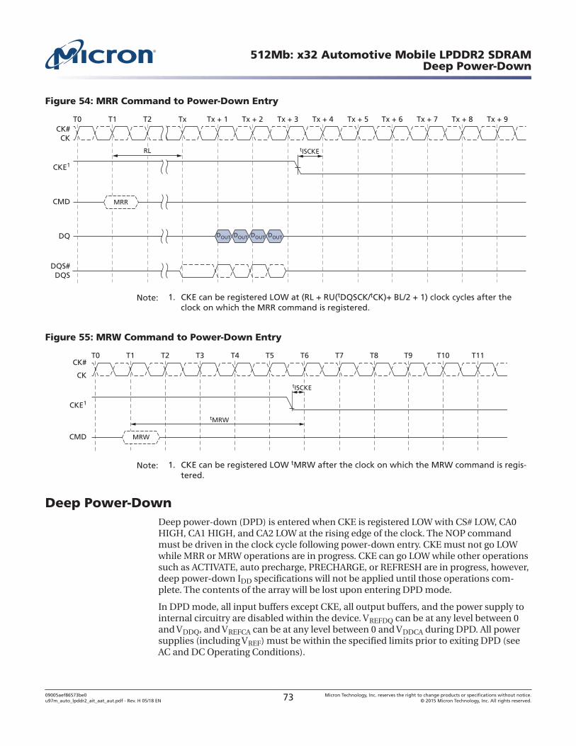
Figure 54: MRR Command to Power-Down Entry
CK#CK
CKE1
T0 T1 T2 Tx Tx + 1 Tx + 2 Tx + 3 Tx + 4 Tx + 5 Tx + 6 Tx + 7 Tx + 8 Tx + 9
CMD
DQ
DQS#DQS
MRR
DOUT DOUT DOUT DOUT
RL tISCKE
Note: 1. CKE can be registered LOW at (RL + RU(tDQSCK/tCK)+ BL/2 + 1) clock cycles after theclock on which the MRR command is registered.
Figure 55: MRW Command to Power-Down Entry
CK#
CKE1
CMD
tMRW
MRW
tISCKE
T0 T1 T2 T3 T4 T5 T6 T7 T8 T9 T10 T11
CK
Note: 1. CKE can be registered LOW tMRW after the clock on which the MRW command is regis-tered.
Deep Power-DownDeep power-down (DPD) is entered when CKE is registered LOW with CS# LOW, CA0HIGH, CA1 HIGH, and CA2 LOW at the rising edge of the clock. The NOP commandmust be driven in the clock cycle following power-down entry. CKE must not go LOWwhile MRR or MRW operations are in progress. CKE can go LOW while other operationssuch as ACTIVATE, auto precharge, PRECHARGE, or REFRESH are in progress, however,deep power-down IDD specifications will not be applied until those operations com-plete. The contents of the array will be lost upon entering DPD mode.
In DPD mode, all input buffers except CKE, all output buffers, and the power supply tointernal circuitry are disabled within the device. VREFDQ can be at any level between 0and VDDQ, and VREFCA can be at any level between 0 and VDDCA during DPD. All powersupplies (including VREF) must be within the specified limits prior to exiting DPD (seeAC and DC Operating Conditions).
512Mb: x32 Automotive Mobile LPDDR2 SDRAMDeep Power-Down
09005aef86573be0u97m_auto_lpddr2_ait_aat_aut.pdf - Rev. H 05/18 EN 73 Micron Technology, Inc. reserves the right to change products or specifications without notice.
© 2015 Micron Technology, Inc. All rights reserved.
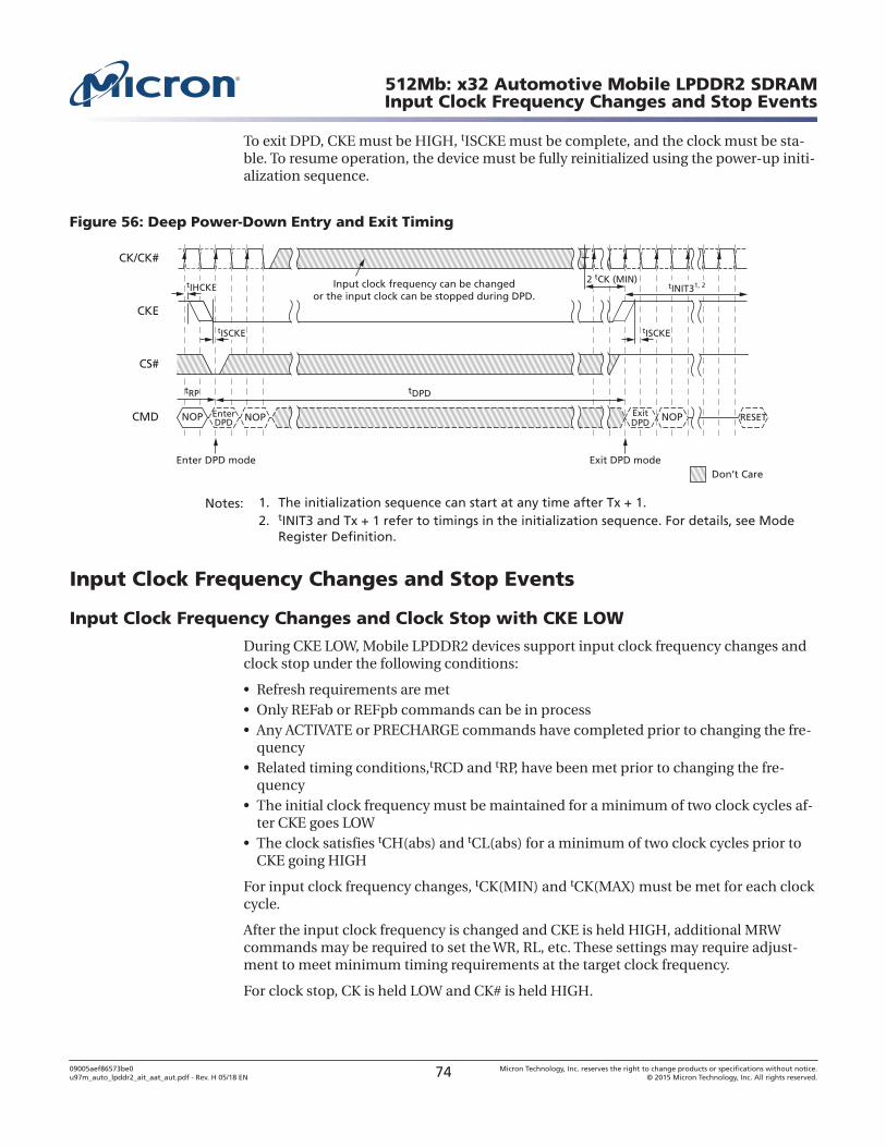
To exit DPD, CKE must be HIGH, tISCKE must be complete, and the clock must be sta-ble. To resume operation, the device must be fully reinitialized using the power-up initi-alization sequence.
Figure 56: Deep Power-Down Entry and Exit Timing
RESETNOPEnterDPD NOP
Enter DPD mode
Input clock frequency can be changedor the input clock can be stopped during DPD.
NOP
CK/CK#
CKE
CS#
CMD
tDPD
tINIT31, 2tIHCKE
tISCKE
tRP
tISCKE
Exit DPD modeDon’t Care
2 tCK (MIN)
ExitDPD
Notes: 1. The initialization sequence can start at any time after Tx + 1.2. tINIT3 and Tx + 1 refer to timings in the initialization sequence. For details, see Mode
Register Definition.
Input Clock Frequency Changes and Stop Events
Input Clock Frequency Changes and Clock Stop with CKE LOW
During CKE LOW, Mobile LPDDR2 devices support input clock frequency changes andclock stop under the following conditions:
• Refresh requirements are met• Only REFab or REFpb commands can be in process• Any ACTIVATE or PRECHARGE commands have completed prior to changing the fre-
quency• Related timing conditions,tRCD and tRP, have been met prior to changing the fre-
quency• The initial clock frequency must be maintained for a minimum of two clock cycles af-
ter CKE goes LOW• The clock satisfies tCH(abs) and tCL(abs) for a minimum of two clock cycles prior to
CKE going HIGH
For input clock frequency changes, tCK(MIN) and tCK(MAX) must be met for each clockcycle.
After the input clock frequency is changed and CKE is held HIGH, additional MRWcommands may be required to set the WR, RL, etc. These settings may require adjust-ment to meet minimum timing requirements at the target clock frequency.
For clock stop, CK is held LOW and CK# is held HIGH.
512Mb: x32 Automotive Mobile LPDDR2 SDRAMInput Clock Frequency Changes and Stop Events
09005aef86573be0u97m_auto_lpddr2_ait_aat_aut.pdf - Rev. H 05/18 EN 74 Micron Technology, Inc. reserves the right to change products or specifications without notice.
© 2015 Micron Technology, Inc. All rights reserved.
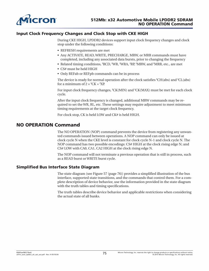
Input Clock Frequency Changes and Clock Stop with CKE HIGH
During CKE HIGH, LPDDR2 devices support input clock frequency changes and clockstop under the following conditions:
• REFRESH requirements are met• Any ACTIVATE, READ, WRITE, PRECHARGE, MRW, or MRR commands must have
completed, including any associated data bursts, prior to changing the frequency• Related timing conditions, tRCD, tWR, tWRA, tRP, tMRW, and tMRR, etc., are met• CS# must be held HIGH• Only REFab or REFpb commands can be in process
The device is ready for normal operation after the clock satisfies tCH(abs) and tCL(abs)for a minimum of 2 × tCK + tXP.
For input clock frequency changes, tCK(MIN) and tCK(MAX) must be met for each clockcycle.
After the input clock frequency is changed, additional MRW commands may be re-quired to set the WR, RL, etc. These settings may require adjustment to meet minimumtiming requirements at the target clock frequency.
For clock stop, CK is held LOW and CK# is held HIGH.
NO OPERATION CommandThe NO OPERATION (NOP) command prevents the device from registering any unwan-ted commands issued between operations. A NOP command can only be issued atclock cycle N when the CKE level is constant for clock cycle N-1 and clock cycle N. TheNOP command has two possible encodings: CS# HIGH at the clock rising edge N; andCS# LOW with CA0, CA1, CA2 HIGH at the clock rising edge N.
The NOP command will not terminate a previous operation that is still in process, suchas a READ burst or WRITE burst cycle.
Simplified Bus Interface State Diagram
The state diagram (see Figure 57 (page 76)) provides a simplified illustration of the businterface, supported state transitions, and the commands that control them. For a com-plete description of device behavior, use the information provided in the state diagramwith the truth tables and timing specifications.
The truth tables describe device behavior and applicable restrictions when consideringthe actual state of all banks.
512Mb: x32 Automotive Mobile LPDDR2 SDRAMNO OPERATION Command
09005aef86573be0u97m_auto_lpddr2_ait_aat_aut.pdf - Rev. H 05/18 EN 75 Micron Technology, Inc. reserves the right to change products or specifications without notice.
© 2015 Micron Technology, Inc. All rights reserved.
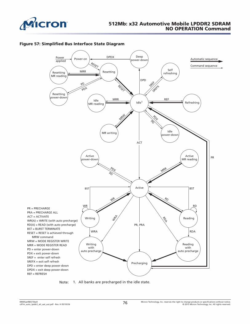
Figure 57: Simplified Bus Interface State Diagram
Powerapplied
ResettingSelf
refreshing
Refreshing
Power-on
ResettingMR reading
IdleMR reading
ActiveMR reading
Activepower-down
Idlepower-down
Deeppower-down
Idle1
Active BSTBST
PR
Precharging
MR writing
Writing Reading
Readingwith
auto precharge
Writingwith
auto precharge
Resettingpower-down
RESET
MRR
RESET
MRR
MRW
MRR
WR RD
PD
PDX
PDXPD
PDXPD
DPDX
DPD
SREF
REF
WRA
WRA
RDA
RDA
SREF
X
RDWR
Automatic sequence
Command sequence
PR = PRECHARGEPRA = PRECHARGE ALLACT = ACTIVATEWR(A) = WRITE (with auto precharge)RD(A) = READ (with auto precharge)BST = BURST TERMINATERESET = RESET is achieved through MRW commandMRW = MODE REGISTER WRITEMRR = MODE REGISTER READPD = enter power-downPDX = exit power-downSREF = enter self refreshSREFX = exit self refreshDPD = enter deep power-downDPDX = exit deep power-downREF = REFRESH
PR, PRA
ACT
Note: 1. All banks are precharged in the idle state.
512Mb: x32 Automotive Mobile LPDDR2 SDRAMNO OPERATION Command
09005aef86573be0u97m_auto_lpddr2_ait_aat_aut.pdf - Rev. H 05/18 EN 76 Micron Technology, Inc. reserves the right to change products or specifications without notice.
© 2015 Micron Technology, Inc. All rights reserved.
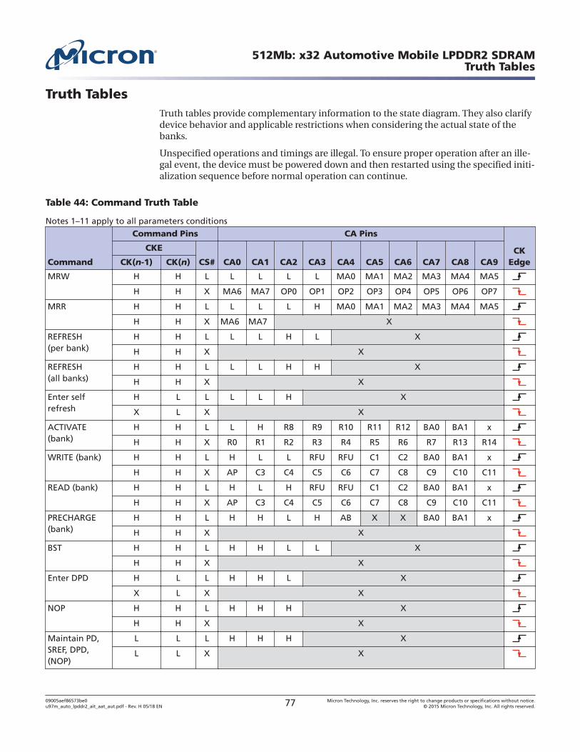
Truth TablesTruth tables provide complementary information to the state diagram. They also clarifydevice behavior and applicable restrictions when considering the actual state of thebanks.
Unspecified operations and timings are illegal. To ensure proper operation after an ille-gal event, the device must be powered down and then restarted using the specified initi-alization sequence before normal operation can continue.
Table 44: Command Truth Table
Notes 1–11 apply to all parameters conditions
Command
Command Pins CA Pins
CKEdge
CKE
CS# CA0 CA1 CA2 CA3 CA4 CA5 CA6 CA7 CA8 CA9CK(n-1) CK(n)
MRW H H L L L L L MA0 MA1 MA2 MA3 MA4 MA5
H H X MA6 MA7 OP0 OP1 OP2 OP3 OP4 OP5 OP6 OP7
MRR H H L L L L H MA0 MA1 MA2 MA3 MA4 MA5
H H X MA6 MA7 X
REFRESH(per bank)
H H L L L H L X
H H X X
REFRESH(all banks)
H H L L L H H X
H H X X
Enter selfrefresh
H L L L L H X
X L X X
ACTIVATE(bank)
H H L L H R8 R9 R10 R11 R12 BA0 BA1 x
H H X R0 R1 R2 R3 R4 R5 R6 R7 R13 R14
WRITE (bank) H H L H L L RFU RFU C1 C2 BA0 BA1 x
H H X AP C3 C4 C5 C6 C7 C8 C9 C10 C11
READ (bank) H H L H L H RFU RFU C1 C2 BA0 BA1 x
H H X AP C3 C4 C5 C6 C7 C8 C9 C10 C11
PRECHARGE(bank)
H H L H H L H AB X X BA0 BA1 x
H H X X
BST H H L H H L L X
H H X X
Enter DPD H L L H H L X
X L X X
NOP H H L H H H X
H H X X
Maintain PD,SREF, DPD,(NOP)
L L L H H H X
L L X X
512Mb: x32 Automotive Mobile LPDDR2 SDRAMTruth Tables
09005aef86573be0u97m_auto_lpddr2_ait_aat_aut.pdf - Rev. H 05/18 EN 77 Micron Technology, Inc. reserves the right to change products or specifications without notice.
© 2015 Micron Technology, Inc. All rights reserved.
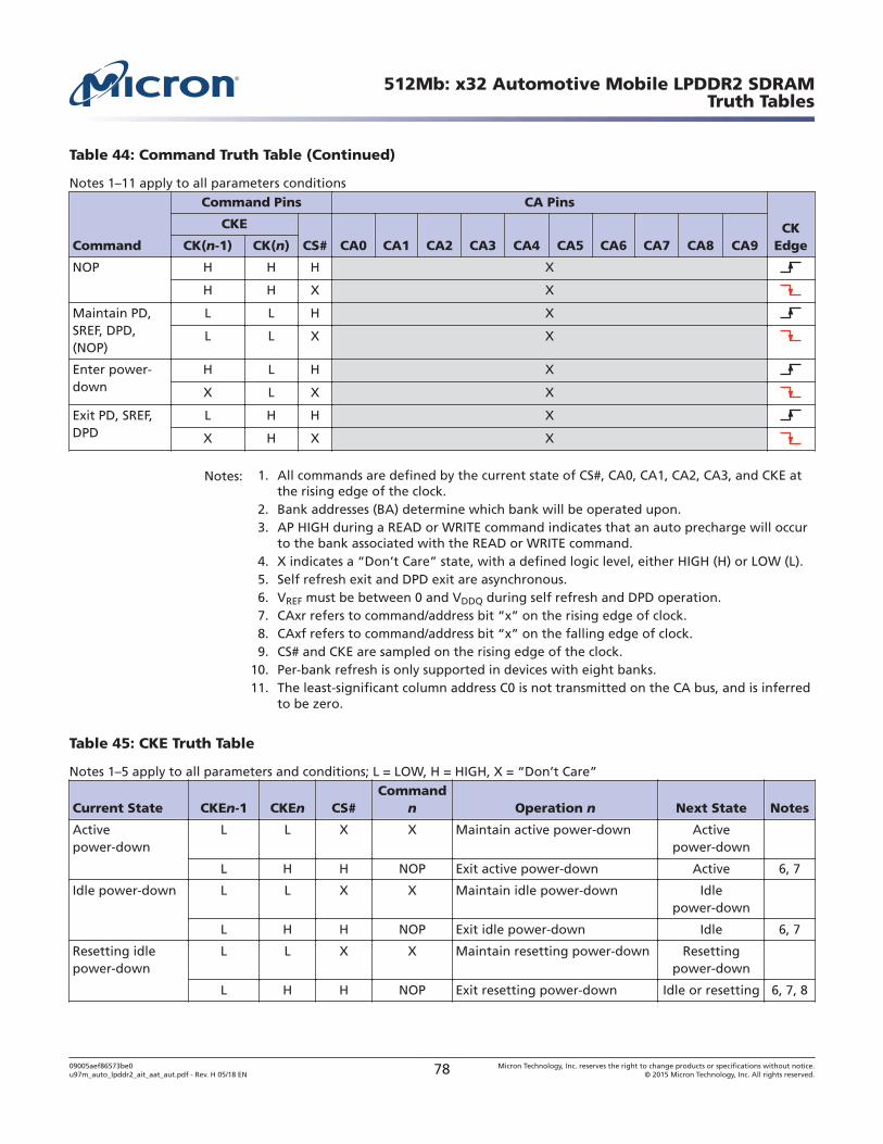
Table 44: Command Truth Table (Continued)
Notes 1–11 apply to all parameters conditions
Command
Command Pins CA Pins
CKEdge
CKE
CS# CA0 CA1 CA2 CA3 CA4 CA5 CA6 CA7 CA8 CA9CK(n-1) CK(n)
NOP H H H X
H H X X
Maintain PD,SREF, DPD,(NOP)
L L H X
L L X X
Enter power-down
H L H X
X L X X
Exit PD, SREF,DPD
L H H X
X H X X
Notes: 1. All commands are defined by the current state of CS#, CA0, CA1, CA2, CA3, and CKE atthe rising edge of the clock.
2. Bank addresses (BA) determine which bank will be operated upon.3. AP HIGH during a READ or WRITE command indicates that an auto precharge will occur
to the bank associated with the READ or WRITE command.4. X indicates a “Don’t Care” state, with a defined logic level, either HIGH (H) or LOW (L).5. Self refresh exit and DPD exit are asynchronous.6. VREF must be between 0 and VDDQ during self refresh and DPD operation.7. CAxr refers to command/address bit “x” on the rising edge of clock.8. CAxf refers to command/address bit “x” on the falling edge of clock.9. CS# and CKE are sampled on the rising edge of the clock.
10. Per-bank refresh is only supported in devices with eight banks.11. The least-significant column address C0 is not transmitted on the CA bus, and is inferred
to be zero.
Table 45: CKE Truth Table
Notes 1–5 apply to all parameters and conditions; L = LOW, H = HIGH, X = “Don’t Care”
Current State CKEn-1 CKEn CS#Command
n Operation n Next State Notes
Activepower-down
L L X X Maintain active power-down Activepower-down
L H H NOP Exit active power-down Active 6, 7
Idle power-down L L X X Maintain idle power-down Idlepower-down
L H H NOP Exit idle power-down Idle 6, 7
Resetting idlepower-down
L L X X Maintain resetting power-down Resettingpower-down
L H H NOP Exit resetting power-down Idle or resetting 6, 7, 8
512Mb: x32 Automotive Mobile LPDDR2 SDRAMTruth Tables
09005aef86573be0u97m_auto_lpddr2_ait_aat_aut.pdf - Rev. H 05/18 EN 78 Micron Technology, Inc. reserves the right to change products or specifications without notice.
© 2015 Micron Technology, Inc. All rights reserved.
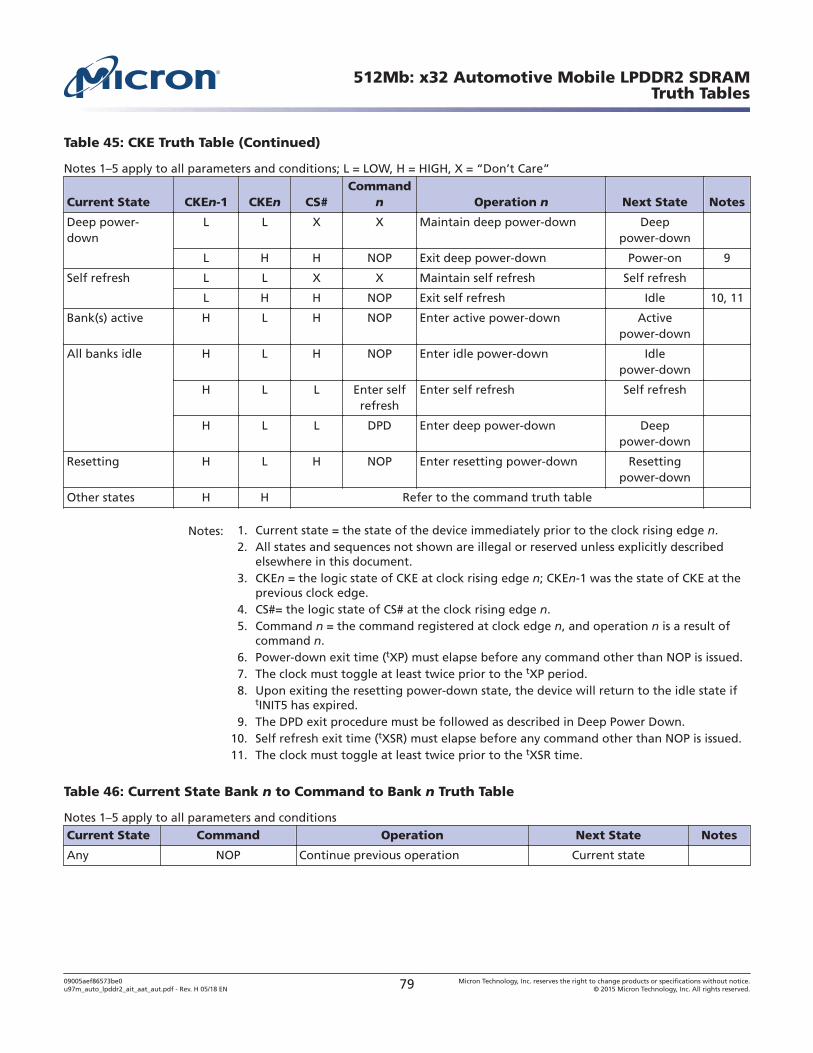
Table 45: CKE Truth Table (Continued)
Notes 1–5 apply to all parameters and conditions; L = LOW, H = HIGH, X = “Don’t Care”
Current State CKEn-1 CKEn CS#Command
n Operation n Next State Notes
Deep power-down
L L X X Maintain deep power-down Deeppower-down
L H H NOP Exit deep power-down Power-on 9
Self refresh L L X X Maintain self refresh Self refresh
L H H NOP Exit self refresh Idle 10, 11
Bank(s) active H L H NOP Enter active power-down Activepower-down
All banks idle H L H NOP Enter idle power-down Idlepower-down
H L L Enter selfrefresh
Enter self refresh Self refresh
H L L DPD Enter deep power-down Deeppower-down
Resetting H L H NOP Enter resetting power-down Resettingpower-down
Other states H H Refer to the command truth table
Notes: 1. Current state = the state of the device immediately prior to the clock rising edge n.2. All states and sequences not shown are illegal or reserved unless explicitly described
elsewhere in this document.3. CKEn = the logic state of CKE at clock rising edge n; CKEn-1 was the state of CKE at the
previous clock edge.4. CS#= the logic state of CS# at the clock rising edge n.5. Command n = the command registered at clock edge n, and operation n is a result of
command n.6. Power-down exit time (tXP) must elapse before any command other than NOP is issued.7. The clock must toggle at least twice prior to the tXP period.8. Upon exiting the resetting power-down state, the device will return to the idle state if
tINIT5 has expired.9. The DPD exit procedure must be followed as described in Deep Power Down.
10. Self refresh exit time (tXSR) must elapse before any command other than NOP is issued.11. The clock must toggle at least twice prior to the tXSR time.
Table 46: Current State Bank n to Command to Bank n Truth Table
Notes 1–5 apply to all parameters and conditionsCurrent State Command Operation Next State Notes
Any NOP Continue previous operation Current state
512Mb: x32 Automotive Mobile LPDDR2 SDRAMTruth Tables
09005aef86573be0u97m_auto_lpddr2_ait_aat_aut.pdf - Rev. H 05/18 EN 79 Micron Technology, Inc. reserves the right to change products or specifications without notice.
© 2015 Micron Technology, Inc. All rights reserved.
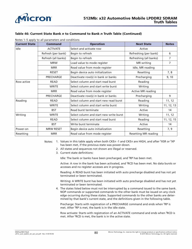
Table 46: Current State Bank n to Command to Bank n Truth Table (Continued)
Notes 1–5 apply to all parameters and conditionsCurrent State Command Operation Next State Notes
Idle ACTIVATE Select and activate row Active
Refresh (per bank) Begin to refresh Refreshing (per bank) 6
Refresh (all banks) Begin to refresh Refreshing (all banks) 7
MRW Load value to mode register MR writing 7
MRR Read value from mode register Idle, MR reading
RESET Begin device auto initialization Resetting 7, 8
PRECHARGE Deactivate row(s) in bank or banks Precharging 9, 10
Row active READ Select column and start read burst Reading
WRITE Select column and start write burst Writing
MRR Read value from mode register Active MR reading
PRECHARGE Deactivate row(s) in bank or banks Precharging 9
Reading READ Select column and start new read burst Reading 11, 12
WRITE Select column and start write burst Writing 11, 12, 13
BST Read burst terminate Active 14
Writing WRITE Select column and start new write burst Writing 11, 12
READ Select column and start read burst Reading 11, 12, 15
BST Write burst terminate Active 14
Power-on MRW RESET Begin device auto initialization Resetting 7, 9
Resetting MRR Read value from mode register Resetting MR reading
Notes: 1. Values in this table apply when both CKEn -1 and CKEn are HIGH, and after tXSR or tXPhas been met, if the previous state was power-down.
2. All states and sequences not shown are illegal or reserved.3. Current state definitions:
Idle: The bank or banks have been precharged, and tRP has been met.
Active: A row in the bank has been activated, and tRCD has been met. No data bursts oraccesses and no register accesses are in progress.
Reading: A READ burst has been initiated with auto precharge disabled and has not yetterminated or been terminated.
Writing: A WRITE burst has been initiated with auto precharge disabled and has not yetterminated or been terminated.
4. The states listed below must not be interrupted by a command issued to the same bank.NOP commands or supported commands to the other bank must be issued on any clockedge occurring during these states. Supported commands to the other banks are deter-mined by that bank’s current state, and the definitions given in the following table.
Precharge: Starts with registration of a PRECHARGE command and ends when tRP ismet. After tRP is met, the bank is in the idle state.
Row activate: Starts with registration of an ACTIVATE command and ends when tRCD ismet. After tRCD is met, the bank is in the active state.
512Mb: x32 Automotive Mobile LPDDR2 SDRAMTruth Tables
09005aef86573be0u97m_auto_lpddr2_ait_aat_aut.pdf - Rev. H 05/18 EN 80 Micron Technology, Inc. reserves the right to change products or specifications without notice.
© 2015 Micron Technology, Inc. All rights reserved.
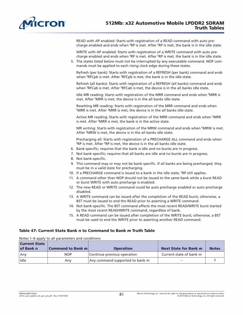
READ with AP enabled: Starts with registration of a READ command with auto pre-charge enabled and ends when tRP is met. After tRP is met, the bank is in the idle state.
WRITE with AP enabled: Starts with registration of a WRITE command with auto pre-charge enabled and ends when tRP is met. After tRP is met, the bank is in the idle state.
5. The states listed below must not be interrupted by any executable command. NOP com-mands must be applied to each rising clock edge during these states.
Refresh (per bank): Starts with registration of a REFRESH (per bank) command and endswhen tRFCpb is met. After tRFCpb is met, the bank is in the idle state.
Refresh (all banks): Starts with registration of a REFRESH (all banks) command and endswhen tRFCab is met. After tRFCab is met, the device is in the all banks idle state.
Idle MR reading: Starts with registration of the MRR command and ends when tMRR ismet. After tMRR is met, the device is in the all banks idle state.
Resetting MR reading: Starts with registration of the MRR command and ends whentMRR is met. After tMRR is met, the device is in the all banks idle state.
Active MR reading: Starts with registration of the MRR command and ends when tMRRis met. After tMRR is met, the bank is in the active state.
MR writing: Starts with registration of the MRW command and ends when tMRW is met.After tMRW is met, the device is in the all banks idle state.
Precharging all: Starts with registration of a PRECHARGE ALL command and ends whentRP is met. After tRP is met, the device is in the all banks idle state.
6. Bank-specific; requires that the bank is idle and no bursts are in progress.7. Not bank-specific; requires that all banks are idle and no bursts are in progress.8. Not bank-specific.9. This command may or may not be bank specific. If all banks are being precharged, they
must be in a valid state for precharging.10. If a PRECHARGE command is issued to a bank in the idle state, tRP still applies.11. A command other than NOP should not be issued to the same bank while a burst READ
or burst WRITE with auto precharge is enabled.12. The new READ or WRITE command could be auto precharge enabled or auto precharge
disabled.13. A WRITE command can be issued after the completion of the READ burst; otherwise, a
BST must be issued to end the READ prior to asserting a WRITE command.14. Not bank-specific. The BST command affects the most recent READ/WRITE burst started
by the most recent READ/WRITE command, regardless of bank.15. A READ command can be issued after completion of the WRITE burst; otherwise, a BST
must be used to end the WRITE prior to asserting another READ command.
Table 47: Current State Bank n to Command to Bank m Truth Table
Notes 1–6 apply to all parameters and conditionsCurrent Stateof Bank n Command to Bank m Operation Next State for Bank m Notes
Any NOP Continue previous operation Current state of bank m
Idle Any Any command supported to bank m – 7
512Mb: x32 Automotive Mobile LPDDR2 SDRAMTruth Tables
09005aef86573be0u97m_auto_lpddr2_ait_aat_aut.pdf - Rev. H 05/18 EN 81 Micron Technology, Inc. reserves the right to change products or specifications without notice.
© 2015 Micron Technology, Inc. All rights reserved.
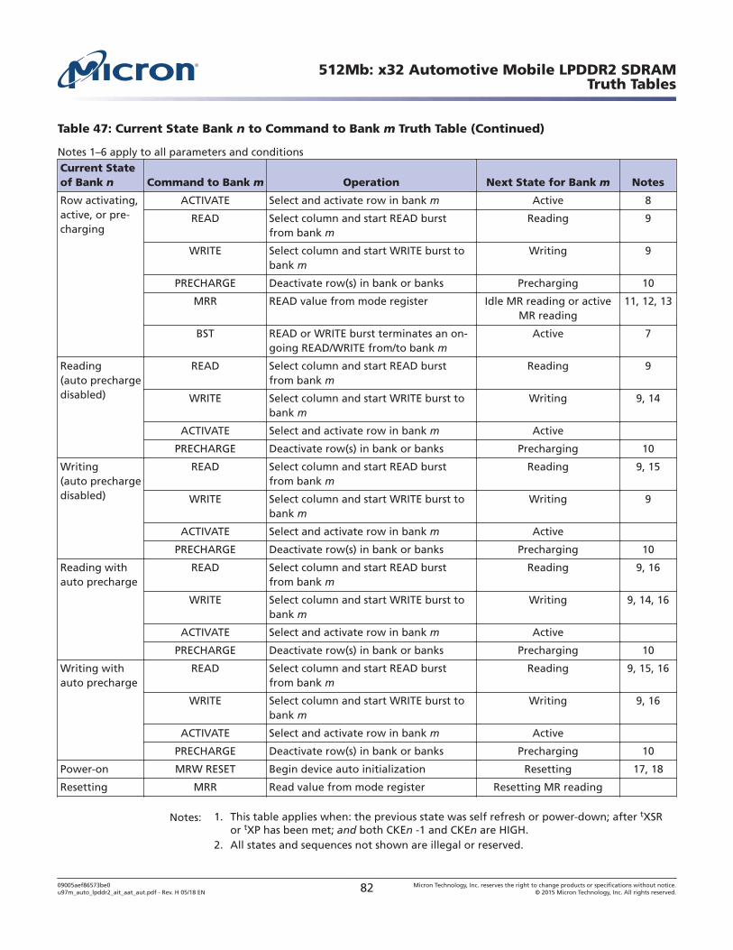
Table 47: Current State Bank n to Command to Bank m Truth Table (Continued)
Notes 1–6 apply to all parameters and conditionsCurrent Stateof Bank n Command to Bank m Operation Next State for Bank m Notes
Row activating,active, or pre-charging
ACTIVATE Select and activate row in bank m Active 8
READ Select column and start READ burstfrom bank m
Reading 9
WRITE Select column and start WRITE burst tobank m
Writing 9
PRECHARGE Deactivate row(s) in bank or banks Precharging 10
MRR READ value from mode register Idle MR reading or activeMR reading
11, 12, 13
BST READ or WRITE burst terminates an on-going READ/WRITE from/to bank m
Active 7
Reading(auto prechargedisabled)
READ Select column and start READ burstfrom bank m
Reading 9
WRITE Select column and start WRITE burst tobank m
Writing 9, 14
ACTIVATE Select and activate row in bank m Active
PRECHARGE Deactivate row(s) in bank or banks Precharging 10
Writing(auto prechargedisabled)
READ Select column and start READ burstfrom bank m
Reading 9, 15
WRITE Select column and start WRITE burst tobank m
Writing 9
ACTIVATE Select and activate row in bank m Active
PRECHARGE Deactivate row(s) in bank or banks Precharging 10
Reading withauto precharge
READ Select column and start READ burstfrom bank m
Reading 9, 16
WRITE Select column and start WRITE burst tobank m
Writing 9, 14, 16
ACTIVATE Select and activate row in bank m Active
PRECHARGE Deactivate row(s) in bank or banks Precharging 10
Writing withauto precharge
READ Select column and start READ burstfrom bank m
Reading 9, 15, 16
WRITE Select column and start WRITE burst tobank m
Writing 9, 16
ACTIVATE Select and activate row in bank m Active
PRECHARGE Deactivate row(s) in bank or banks Precharging 10
Power-on MRW RESET Begin device auto initialization Resetting 17, 18
Resetting MRR Read value from mode register Resetting MR reading
Notes: 1. This table applies when: the previous state was self refresh or power-down; after tXSRor tXP has been met; and both CKEn -1 and CKEn are HIGH.
2. All states and sequences not shown are illegal or reserved.
512Mb: x32 Automotive Mobile LPDDR2 SDRAMTruth Tables
09005aef86573be0u97m_auto_lpddr2_ait_aat_aut.pdf - Rev. H 05/18 EN 82 Micron Technology, Inc. reserves the right to change products or specifications without notice.
© 2015 Micron Technology, Inc. All rights reserved.
3. Current state definitions:
Idle: The bank has been precharged and tRP has been met.
Active: A row in the bank has been activated, tRCD has been met, no data bursts or ac-cesses and no register accesses are in progress.
Read: A READ burst has been initiated with auto precharge disabled and the READ hasnot yet terminated or been terminated.
Write: A WRITE burst has been initiated with auto precharge disabled and the WRITEhas not yet terminated or been terminated.
4. Refresh, self refresh, and MRW commands can only be issued when all banks are idle.5. A BST command cannot be issued to another bank; it applies only to the bank represen-
ted by the current state.6. The states listed below must not be interrupted by any executable command. NOP com-
mands must be applied during each clock cycle while in these states:
Idle MRR: Starts with registration of the MRR command and ends when tMRR has beenmet. After tMRR is met, the device is in the all banks idle state.
Reset MRR: Starts with registration of the MRR command and ends when tMRR has beenmet. After tMRR is met, the device is in the all banks idle state.
Active MRR: Starts with registration of the MRR command and ends when tMRR hasbeen met. After tMRR is met, the bank is in the active state.
MRW: Starts with registration of the MRW command and ends when tMRW has beenmet. After tMRW is met, the device is in the all banks idle state.
7. BST is supported only if a READ or WRITE burst is ongoing.8. tRRD must be met between the ACTIVATE command to bank n and any subsequent
ACTIVATE command to bank m.9. READs or WRITEs listed in the command column include READs and WRITEs with or
without auto precharge enabled.10. This command may or may not be bank-specific. If all banks are being precharged, they
must be in a valid state for precharging.11. MRR is supported in the row-activating state.12. MRR is supported in the precharging state.13. The next state for bank m depends on the current state of bank m (idle, row-activating,
precharging, or active).14. A WRITE command can be issued after the completion of the READ burst; otherwise a
BST must be issued to end the READ prior to asserting a WRITE command.15. A READ command can be issued after the completion of the WRITE burst; otherwise, a
BST must be issued to end the WRITE prior to asserting another READ command.16. A READ with auto precharge enabled or a WRITE with auto precharge enabled can be
followed by any valid command to other banks provided that the timing restrictions inthe PRECHARGE and Auto Precharge Clarification table are met.
17. Not bank-specific; requires that all banks are idle and no bursts are in progress.18. RESET command is achieved through MODE REGISTER WRITE command.
512Mb: x32 Automotive Mobile LPDDR2 SDRAMTruth Tables
09005aef86573be0u97m_auto_lpddr2_ait_aat_aut.pdf - Rev. H 05/18 EN 83 Micron Technology, Inc. reserves the right to change products or specifications without notice.
© 2015 Micron Technology, Inc. All rights reserved.
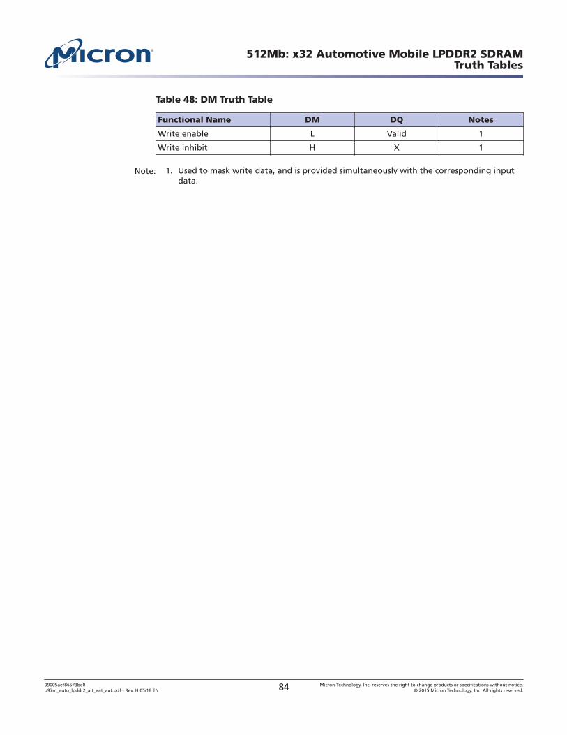
Table 48: DM Truth Table
Functional Name DM DQ Notes
Write enable L Valid 1
Write inhibit H X 1
Note: 1. Used to mask write data, and is provided simultaneously with the corresponding inputdata.
512Mb: x32 Automotive Mobile LPDDR2 SDRAMTruth Tables
09005aef86573be0u97m_auto_lpddr2_ait_aat_aut.pdf - Rev. H 05/18 EN 84 Micron Technology, Inc. reserves the right to change products or specifications without notice.
© 2015 Micron Technology, Inc. All rights reserved.
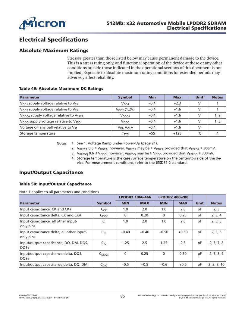
Electrical Specifications
Absolute Maximum Ratings
Stresses greater than those listed below may cause permanent damage to the device.This is a stress rating only, and functional operation of the device at these or any otherconditions outside those indicated in the operational sections of this document is notimplied. Exposure to absolute maximum rating conditions for extended periods mayadversely affect reliability.
Table 49: Absolute Maximum DC Ratings
Parameter Symbol Min Max Unit Notes
VDD1 supply voltage relative to VSS VDD1 –0.4 +2.3 V 1
VDD2 supply voltage relative to VSS VDD2 (1.2V) –0.4 +1.6 V 1
VDDCA supply voltage relative to VSSCA VDDCA –0.4 +1.6 V 1, 2
VDDQ supply voltage relative to VSSQ VDDQ –0.4 +1.6 V 1, 3
Voltage on any ball relative to VSS VIN, VOUT –0.4 +1.6 V
Storage temperature TSTG –55 +125 ˚C 4
Notes: 1. See 1. Voltage Ramp under Power-Up (page 21).2. VREFCA 0.6 ≤ VDDCA; however, VREFCA may be ≥ VDDCA provided that VREFCA ≤ 300mV.3. VREFDQ 0.6 ≤ VDDQ; however, VREFDQ may be ≥ VDDQ provided that VREFDQ ≤ 300mV.4. Storage temperature is the case surface temperature on the center/top side of the de-
vice. For measurement conditions, refer to the JESD51-2 standard.
Input/Output Capacitance
Table 50: Input/Output Capacitance
Note 1 applies to all parameters and conditions
Parameter Symbol
LPDDR2 1066-466 LPDDR2 400-200
Unit NotesMIN MAX MIN MAX
Input capacitance, CK and CK# CCK 1.0 2.0 1.0 2.0 pF 2, 3
Input capacitance delta, CK and CK# CDCK 0 0.20 0 0.25 pF 2, 3, 4
Input capacitance, all other input-only pins
CI 1.0 2.0 1.0 2.0 pF 2, 3, 5
Input capacitance delta, all other input-only pins
CDI –0.40 +0.40 –0.50 +0.50 pF 2, 3, 6
Input/output capacitance, DQ, DM, DQS,DQS#
CIO 1.25 2.5 1.25 2.5 pF 2, 3, 7, 8
Input/output capacitance delta, DQS,DQS#
CDDQS 0 0.25 0 0.30 pF 2, 3, 8, 9
Input/output capacitance delta, DQ, DM CDIO –0.5 +0.5 –0.6 +0.6 pF 2, 3, 8, 10
512Mb: x32 Automotive Mobile LPDDR2 SDRAMElectrical Specifications
09005aef86573be0u97m_auto_lpddr2_ait_aat_aut.pdf - Rev. H 05/18 EN 85 Micron Technology, Inc. reserves the right to change products or specifications without notice.
© 2015 Micron Technology, Inc. All rights reserved.
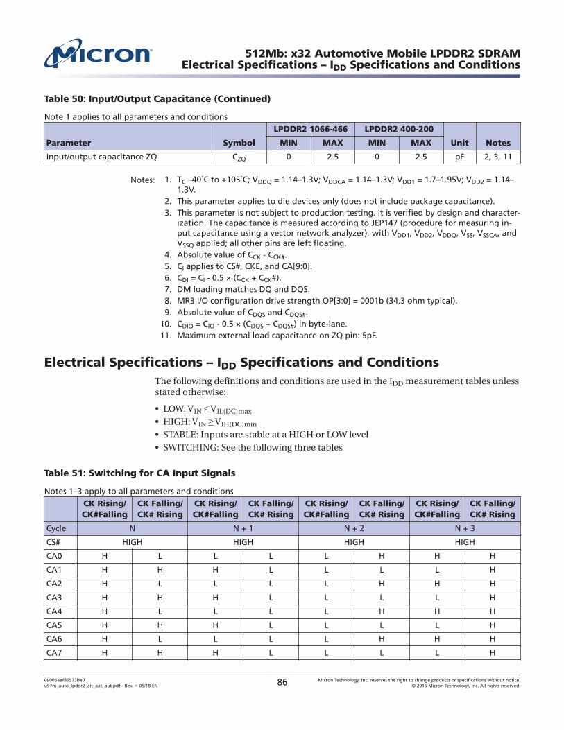
Table 50: Input/Output Capacitance (Continued)
Note 1 applies to all parameters and conditions
Parameter Symbol
LPDDR2 1066-466 LPDDR2 400-200
Unit NotesMIN MAX MIN MAX
Input/output capacitance ZQ CZQ 0 2.5 0 2.5 pF 2, 3, 11
Notes: 1. TC –40˚C to +105˚C; VDDQ = 1.14–1.3V; VDDCA = 1.14–1.3V; VDD1 = 1.7–1.95V; VDD2 = 1.14–1.3V.
2. This parameter applies to die devices only (does not include package capacitance).3. This parameter is not subject to production testing. It is verified by design and character-
ization. The capacitance is measured according to JEP147 (procedure for measuring in-put capacitance using a vector network analyzer), with VDD1, VDD2, VDDQ, VSS, VSSCA, andVSSQ applied; all other pins are left floating.
4. Absolute value of CCK - CCK#.5. CI applies to CS#, CKE, and CA[9:0].6. CDI = CI - 0.5 × (CCK + CCK#).7. DM loading matches DQ and DQS.8. MR3 I/O configuration drive strength OP[3:0] = 0001b (34.3 ohm typical).9. Absolute value of CDQS and CDQS#.
10. CDIO = CIO - 0.5 × (CDQS + CDQS#) in byte-lane.11. Maximum external load capacitance on ZQ pin: 5pF.
Electrical Specifications – IDD Specifications and ConditionsThe following definitions and conditions are used in the IDD measurement tables unlessstated otherwise:
• LOW: VIN VIL(DC)max
• HIGH: VIN VIH(DC)min
• STABLE: Inputs are stable at a HIGH or LOW level• SWITCHING: See the following three tables
Table 51: Switching for CA Input Signals
Notes 1–3 apply to all parameters and conditions
CK Rising/CK#Falling
CK Falling/CK# Rising
CK Rising/CK#Falling
CK Falling/CK# Rising
CK Rising/CK#Falling
CK Falling/CK# Rising
CK Rising/CK#Falling
CK Falling/CK# Rising
Cycle N N + 1 N + 2 N + 3
CS# HIGH HIGH HIGH HIGH
CA0 H L L L L H H H
CA1 H H H L L L L H
CA2 H L L L L H H H
CA3 H H H L L L L H
CA4 H L L L L H H H
CA5 H H H L L L L H
CA6 H L L L L H H H
CA7 H H H L L L L H
512Mb: x32 Automotive Mobile LPDDR2 SDRAMElectrical Specifications – IDD Specifications and Conditions
09005aef86573be0u97m_auto_lpddr2_ait_aat_aut.pdf - Rev. H 05/18 EN 86 Micron Technology, Inc. reserves the right to change products or specifications without notice.
© 2015 Micron Technology, Inc. All rights reserved.
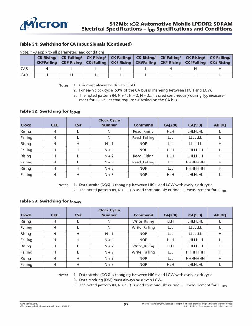
Table 51: Switching for CA Input Signals (Continued)
Notes 1–3 apply to all parameters and conditions
CK Rising/CK#Falling
CK Falling/CK# Rising
CK Rising/CK#Falling
CK Falling/CK# Rising
CK Rising/CK#Falling
CK Falling/CK# Rising
CK Rising/CK#Falling
CK Falling/CK# Rising
CA8 H L L L L H H H
CA9 H H H L L L L H
Notes: 1. CS# must always be driven HIGH.2. For each clock cycle, 50% of the CA bus is changing between HIGH and LOW.3. The noted pattern (N, N + 1, N + 2, N + 3...) is used continuously during IDD measure-
ment for IDD values that require switching on the CA bus.
Table 52: Switching for IDD4R
Clock CKE CS#Clock Cycle
Number Command CA[2:0] CA[9:3] All DQ
Rising H L N Read_Rising HLH LHLHLHL L
Falling H L N Read_Falling LLL LLLLLLL L
Rising H H N +1 NOP LLL LLLLLLL H
Falling H H N + 1 NOP HLH LHLLHLH L
Rising H L N + 2 Read_Rising HLH LHLLHLH H
Falling H L N + 2 Read_Falling LLL HHHHHHH H
Rising H H N + 3 NOP LLL HHHHHHH H
Falling H H N + 3 NOP HLH LHLHLHL L
Notes: 1. Data strobe (DQS) is changing between HIGH and LOW with every clock cycle.2. The noted pattern (N, N + 1...) is used continuously during IDD measurement for IDD4R.
Table 53: Switching for IDD4W
Clock CKE CS#Clock Cycle
Number Command CA[2:0] CA[9:3] All DQ
Rising H L N Write_Rising LLH LHLHLHL L
Falling H L N Write_Falling LLL LLLLLLL L
Rising H H N +1 NOP LLL LLLLLLL H
Falling H H N + 1 NOP HLH LHLLHLH L
Rising H L N + 2 Write_Rising LLH LHLLHLH H
Falling H L N + 2 Write_Falling LLL HHHHHHH H
Rising H H N + 3 NOP LLL HHHHHHH H
Falling H H N + 3 NOP HLH LHLHLHL L
Notes: 1. Data strobe (DQS) is changing between HIGH and LOW with every clock cycle.2. Data masking (DM) must always be driven LOW.3. The noted pattern (N, N + 1...) is used continuously during IDD measurement for IDD4W.
512Mb: x32 Automotive Mobile LPDDR2 SDRAMElectrical Specifications – IDD Specifications and Conditions
09005aef86573be0u97m_auto_lpddr2_ait_aat_aut.pdf - Rev. H 05/18 EN 87 Micron Technology, Inc. reserves the right to change products or specifications without notice.
© 2015 Micron Technology, Inc. All rights reserved.
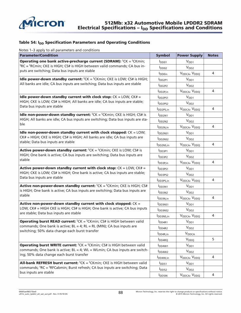
Table 54: IDD Specification Parameters and Operating Conditions
Notes 1–3 apply to all parameters and conditionsParameter/Condition Symbol Power Supply Notes
Operating one bank active-precharge current (SDRAM): tCK = tCKmin;tRC = tRCmin; CKE is HIGH; CS# is HIGH between valid commands; CA bus in-puts are switching; Data bus inputs are stable
IDD01 VDD1
IDD02 VDD2
IDD0in VDDCA, VDDQ 4
Idle power-down standby current: tCK = tCKmin; CKE is LOW; CS# is HIGH;All banks are idle; CA bus inputs are switching; Data bus inputs are stable
IDD2P1 VDD1
IDD2P2 VDD2
IDD2P,in VDDCA, VDDQ 4
Idle power-down standby current with clock stop: CK = LOW, CK# =HIGH; CKE is LOW; CS# is HIGH; All banks are idle; CA bus inputs are stable;Data bus inputs are stable
IDD2PS1 VDD1
IDD2PS2 VDD2
IDD2PS,in VDDCA, VDDQ 4
Idle non-power-down standby current: tCK = tCKmin; CKE is HIGH; CS# isHIGH; All banks are idle; CA bus inputs are switching; Data bus inputs are sta-ble
IDD2N1 VDD1
IDD2N2 VDD2
IDD2N,in VDDCA, VDDQ 4
Idle non-power-down standby current with clock stopped: CK = LOW;CK# = HIGH; CKE is HIGH; CS# is HIGH; All banks are idle; CA bus inputs arestable; Data bus inputs are stable
IDD2NS1 VDD1
IDD2NS2 VDD2
IDD2NS,in VDDCA, VDDQ 4
Active power-down standby current: tCK = tCKmin; CKE is LOW; CS# isHIGH; One bank is active; CA bus inputs are switching; Data bus inputs arestable
IDD3P1 VDD1
IDD3P2 VDD2
IDD3P,in VDDCA, VDDQ 4
Active power-down standby current with clock stop: CK = LOW, CK# =HIGH; CKE is LOW; CS# is HIGH; One bank is active; CA bus inputs are stable;Data bus inputs are stable
IDD3PS1 VDD1
IDD3PS2 VDD2
IDD3PS,in VDDCA, VDDQ 4
Active non-power-down standby current: tCK = tCKmin; CKE is HIGH; CS#is HIGH; One bank is active; CA bus inputs are switching; Data bus inputs arestable
IDD3N1 VDD1
IDD3N2 VDD2
IDD3N,in VDDCA, VDDQ 4
Active non-power-down standby current with clock stopped: CK =LOW, CK# = HIGH CKE is HIGH; CS# is HIGH; One bank is active; CA bus inputsare stable; Data bus inputs are stable
IDD3NS1 VDD1
IDD3NS2 VDD2
IDD3NS,in VDDCA, VDDQ 4
Operating burst READ current: tCK = tCKmin; CS# is HIGH between validcommands; One bank is active; BL = 4; RL = RL (MIN); CA bus inputs areswitching; 50% data change each burst transfer
IDD4R1 VDD1
IDD4R2 VDD2
IDD4R,in VDDCA
IDD4RQ VDDQ 5
Operating burst WRITE current: tCK = tCKmin; CS# is HIGH between validcommands; One bank is active; BL = 4; WL = WLmin; CA bus inputs are switch-ing; 50% data change each burst transfer
IDD4W1 VDD1
IDD4W2 VDD2
IDD4W,in VDDCA, VDDQ 4
All-bank REFRESH burst current: tCK = tCKmin; CKE is HIGH between validcommands; tRC = tRFCabmin; Burst refresh; CA bus inputs are switching; Databus inputs are stable
IDD51 VDD1
IDD52 VDD2
IDD5IN VDDCA, VDDQ 4
512Mb: x32 Automotive Mobile LPDDR2 SDRAMElectrical Specifications – IDD Specifications and Conditions
09005aef86573be0u97m_auto_lpddr2_ait_aat_aut.pdf - Rev. H 05/18 EN 88 Micron Technology, Inc. reserves the right to change products or specifications without notice.
© 2015 Micron Technology, Inc. All rights reserved.
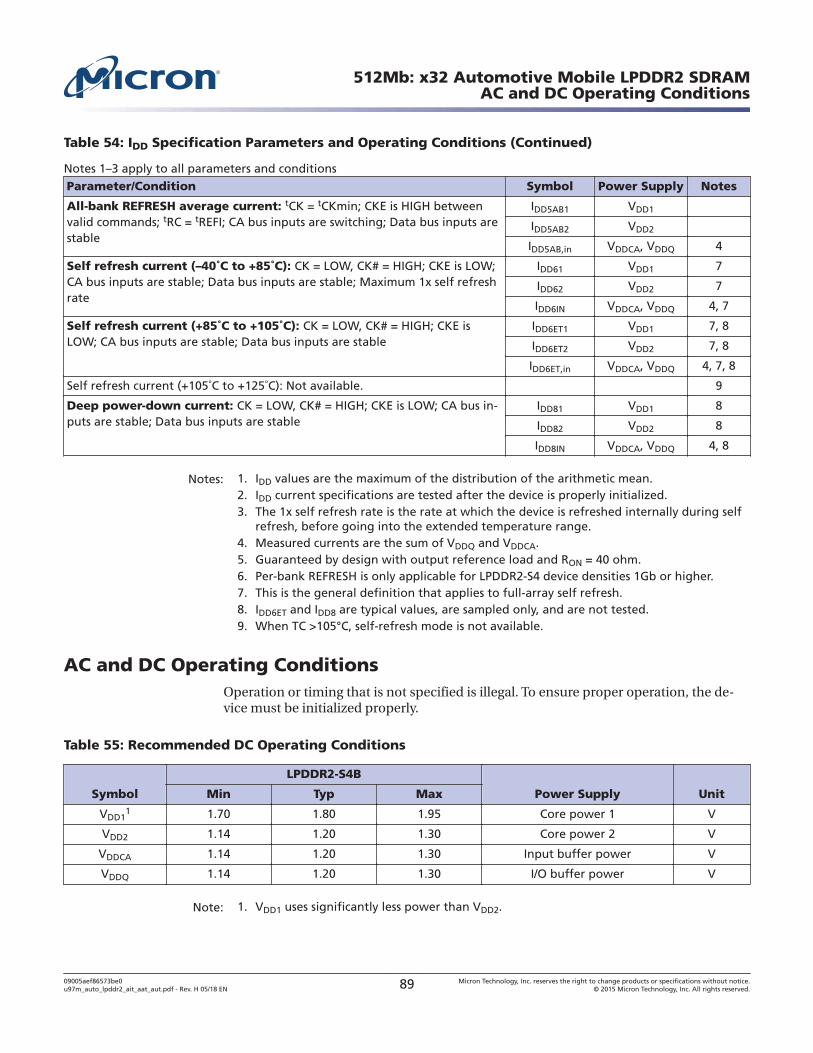
Table 54: IDD Specification Parameters and Operating Conditions (Continued)
Notes 1–3 apply to all parameters and conditionsParameter/Condition Symbol Power Supply Notes
All-bank REFRESH average current: tCK = tCKmin; CKE is HIGH betweenvalid commands; tRC = tREFI; CA bus inputs are switching; Data bus inputs arestable
IDD5AB1 VDD1
IDD5AB2 VDD2
IDD5AB,in VDDCA, VDDQ 4
Self refresh current (–40˚C to +85˚C): CK = LOW, CK# = HIGH; CKE is LOW;CA bus inputs are stable; Data bus inputs are stable; Maximum 1x self refreshrate
IDD61 VDD1 7
IDD62 VDD2 7
IDD6IN VDDCA, VDDQ 4, 7
Self refresh current (+85˚C to +105˚C): CK = LOW, CK# = HIGH; CKE isLOW; CA bus inputs are stable; Data bus inputs are stable
IDD6ET1 VDD1 7, 8
IDD6ET2 VDD2 7, 8
IDD6ET,in VDDCA, VDDQ 4, 7, 8
Self refresh current (+105˚C to +125˚C): Not available. 9
Deep power-down current: CK = LOW, CK# = HIGH; CKE is LOW; CA bus in-puts are stable; Data bus inputs are stable
IDD81 VDD1 8
IDD82 VDD2 8
IDD8IN VDDCA, VDDQ 4, 8
Notes: 1. IDD values are the maximum of the distribution of the arithmetic mean.2. IDD current specifications are tested after the device is properly initialized.3. The 1x self refresh rate is the rate at which the device is refreshed internally during self
refresh, before going into the extended temperature range.4. Measured currents are the sum of VDDQ and VDDCA.5. Guaranteed by design with output reference load and RON = 40 ohm.6. Per-bank REFRESH is only applicable for LPDDR2-S4 device densities 1Gb or higher.7. This is the general definition that applies to full-array self refresh.8. IDD6ET and IDD8 are typical values, are sampled only, and are not tested.9. When TC >105°C, self-refresh mode is not available.
AC and DC Operating ConditionsOperation or timing that is not specified is illegal. To ensure proper operation, the de-vice must be initialized properly.
Table 55: Recommended DC Operating Conditions
Symbol
LPDDR2-S4B
Power Supply UnitMin Typ Max
VDD11 1.70 1.80 1.95 Core power 1 V
VDD2 1.14 1.20 1.30 Core power 2 V
VDDCA 1.14 1.20 1.30 Input buffer power V
VDDQ 1.14 1.20 1.30 I/O buffer power V
Note: 1. VDD1 uses significantly less power than VDD2.
512Mb: x32 Automotive Mobile LPDDR2 SDRAMAC and DC Operating Conditions
09005aef86573be0u97m_auto_lpddr2_ait_aat_aut.pdf - Rev. H 05/18 EN 89 Micron Technology, Inc. reserves the right to change products or specifications without notice.
© 2015 Micron Technology, Inc. All rights reserved.
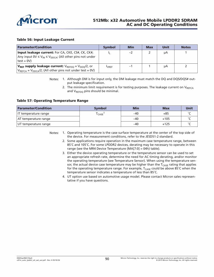
Table 56: Input Leakage Current
Parameter/Condition Symbol Min Max Unit Notes
Input leakage current: For CA, CKE, CS#, CK, CK#;Any input 0V ≤ VIN ≤ VDDCA; (All other pins not undertest = 0V)
IL –2 2 μA 1
VREF supply leakage current: VREFDQ = VDDQ/2, orVREFCA = VDDCA/2; (All other pins not under test = 0V)
IVREF –1 1 μA 2
Notes: 1. Although DM is for input only, the DM leakage must match the DQ and DQS/DQS# out-put leakage specification.
2. The minimum limit requirement is for testing purposes. The leakage current on VREFCAand VREFDQ pins should be minimal.
Table 57: Operating Temperature Range
Parameter/Condition Symbol Min Max Unit
IT temperature range TCASE1 –40 +85 ˚C
AT temperature range –40 +105 ˚C
UT temperature range –40 +125 ˚C
Notes: 1. Operating temperature is the case surface temperature at the center of the top side ofthe device. For measurement conditions, refer to the JESD51-2 standard.
2. Some applications require operation in the maximum case temperature range, between85˚C and 105˚C. For some LPDDR2 devices, derating may be necessary to operate in thisrange (see the MR4 Device Temperature (MA[7:0] = 04h) table).
3. Either the device operating temperature or the temperature sensor can be used to setan appropriate refresh rate, determine the need for AC timing derating, and/or monitorthe operating temperature (see Temperature Sensor). When using the temperature sen-sor, the actual device case temperature may be higher than the TCASE rating that appliesfor the operating temperature range. For example, TCASE could be above 85˚C when thetemperature sensor indicates a temperature of less than 85˚C.
4. UT option use based on automotive usage model. Please contact Micron sales represen-tative if you have questions.
512Mb: x32 Automotive Mobile LPDDR2 SDRAMAC and DC Operating Conditions
09005aef86573be0u97m_auto_lpddr2_ait_aat_aut.pdf - Rev. H 05/18 EN 90 Micron Technology, Inc. reserves the right to change products or specifications without notice.
© 2015 Micron Technology, Inc. All rights reserved.
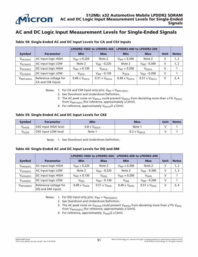
AC and DC Logic Input Measurement Levels for Single-Ended Signals
Table 58: Single-Ended AC and DC Input Levels for CA and CS# Inputs
Symbol Parameter
LPDDR2-1066 to LPDDR2-466 LPDDR2-400 to LPDDR2-200
Unit NotesMin Max Min Max
VIHCA(AC) AC input logic HIGH VREF + 0.220 Note 2 VREF + 0.300 Note 2 V 1, 2
VILCA(AC) AC input logic LOW Note 2 VREF - 0.220 Note 2 VREF - 0.300 V 1, 2
VIHCA(DC) DC input logic HIGH VREF + 0.130 VDDCA VREF + 0.200 VDDCA V 1
VILCA(DC) DC input logic LOW VSSCA VREF - 0.130 VSSCA VREF - 0.200 V 1
VREFCA(DC) Reference voltage forCA and CS# inputs
0.49 × VDDCA 0.51 × VDDCA 0.49 × VDDCA 0.51 × VDDCA V 3, 4
Notes: 1. For CA and CS# input-only pins. VREF = VREFCA(DC).2. See Overshoot and Undershoot Definition.3. The AC peak noise on VREFCA could prevent VREFCA from deviating more than ±1% VDDCA
from VREFCA(DC) (for reference, approximately ±12mV).4. For reference, approximately VDDCA/2 ±12mV.
Table 59: Single-Ended AC and DC Input Levels for CKE
Symbol Parameter Min Max Unit Notes
VIHCKE CKE input HIGH level 0.8 × VDDCA Note 1 V 1
VILCKE CKE input LOW level Note 1 0.2 × VDDCA V 1
Note: 1. See Overshoot and Undershoot Definition.
Table 60: Single-Ended AC and DC Input Levels for DQ and DM
Symbol Parameter
LPDDR2-1066 to LPDDR2-466 LPDDR2-400 to LPDDR2-200
Unit NotesMin Max Min Max
VIHDQ(AC) AC input logic HIGH VREF + 0.220 Note 2 VREF + 0.300 Note 2 V 1, 2
VILDQ(AC) AC input logic LOW Note 2 VREF - 0.220 Note 2 VREF - 0.300 V 1, 2
VIHDQ(DC) DC input logic HIGH VREF + 0.130 VDDQ VREF + 0.200 VDDQ V 1
VILDQ(DC) DC input logic LOW VSSQ VREF - 0.130 VSSQ VREF - 0.200 V 1
VREFDQ(DC) Reference voltage forDQ and DM inputs
0.49 × VDDQ 0.51 × VDDQ 0.49 × VDDQ 0.51 × VDDQ V 3, 4
Notes: 1. For DQ input-only pins. VREF = VREFDQ(DC).2. See Overshoot and Undershoot Definition.3. The AC peak noise on VREFDQ could prevent VREFDQ from deviating more than ±1% VDDQ
from VREFDQ(DC) (for reference, approximately ±12mV).4. For reference, approximately. VDDQ/2 ±12mV.
512Mb: x32 Automotive Mobile LPDDR2 SDRAMAC and DC Logic Input Measurement Levels for Single-Ended
Signals
09005aef86573be0u97m_auto_lpddr2_ait_aat_aut.pdf - Rev. H 05/18 EN 91 Micron Technology, Inc. reserves the right to change products or specifications without notice.
© 2015 Micron Technology, Inc. All rights reserved.
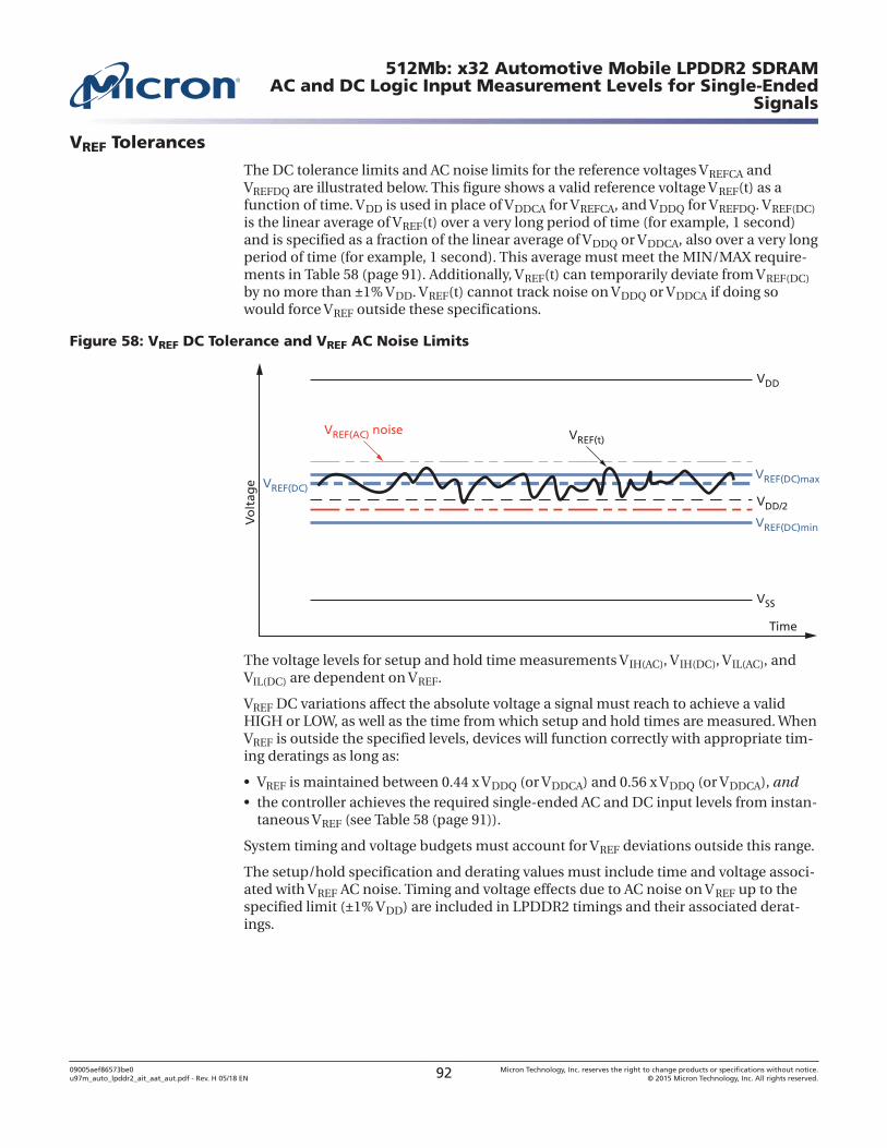
VREF Tolerances
The DC tolerance limits and AC noise limits for the reference voltages VREFCA andVREFDQ are illustrated below. This figure shows a valid reference voltage VREF(t) as afunction of time. VDD is used in place of VDDCA for VREFCA, and VDDQ for VREFDQ. VREF(DC)is the linear average of VREF(t) over a very long period of time (for example, 1 second)and is specified as a fraction of the linear average of VDDQ or VDDCA, also over a very longperiod of time (for example, 1 second). This average must meet the MIN/MAX require-ments in Table 58 (page 91). Additionally, VREF(t) can temporarily deviate from VREF(DC)by no more than ±1% VDD. VREF(t) cannot track noise on VDDQ or VDDCA if doing sowould force VREF outside these specifications.
Figure 58: VREF DC Tolerance and VREF AC Noise Limits
VREF(DC)VREF(DC)max
VDD/2
VDD
VSS
VREF(DC)min
Vo
ltag
e
Time
VREF(AC) noise VREF(t)
The voltage levels for setup and hold time measurements VIH(AC), VIH(DC), VIL(AC), andVIL(DC) are dependent on VREF.
VREF DC variations affect the absolute voltage a signal must reach to achieve a validHIGH or LOW, as well as the time from which setup and hold times are measured. WhenVREF is outside the specified levels, devices will function correctly with appropriate tim-ing deratings as long as:
• VREF is maintained between 0.44 x VDDQ (or VDDCA) and 0.56 x VDDQ (or VDDCA), and• the controller achieves the required single-ended AC and DC input levels from instan-
taneous VREF (see Table 58 (page 91)).
System timing and voltage budgets must account for VREF deviations outside this range.
The setup/hold specification and derating values must include time and voltage associ-ated with VREF AC noise. Timing and voltage effects due to AC noise on VREF up to thespecified limit (±1% VDD) are included in LPDDR2 timings and their associated derat-ings.
512Mb: x32 Automotive Mobile LPDDR2 SDRAMAC and DC Logic Input Measurement Levels for Single-Ended
Signals
09005aef86573be0u97m_auto_lpddr2_ait_aat_aut.pdf - Rev. H 05/18 EN 92 Micron Technology, Inc. reserves the right to change products or specifications without notice.
© 2015 Micron Technology, Inc. All rights reserved.
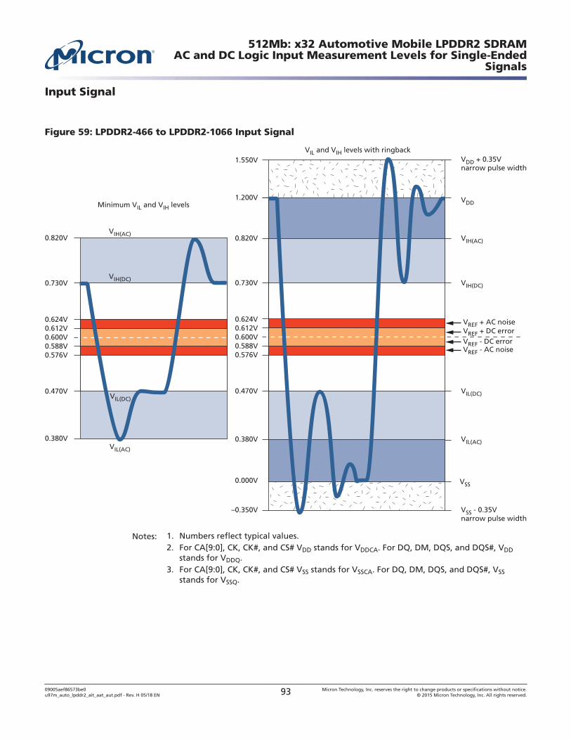
Input Signal
Figure 59: LPDDR2-466 to LPDDR2-1066 Input Signal
0.380V
0.000V
0.470V
0.576V0.588V0.600V0.612V0.624V
0.730V
0.820V
VIL(AC)
VIL(DC)
VREF - AC noiseVREF - DC errorVREF + DC errorVREF + AC noise
VIH(DC)
VIH(AC)
1.200V
1.550V
–0.350V
VDD
VDD + 0.35Vnarrow pulse width
VSS - 0.35V narrow pulse width
VSS
0.380V
0.470V
0.576V0.588V0.600V0.612V0.624V
0.730V
0.820V
Minimum VIL and VIH levels
VIH(DC)
VIH(AC)
VIL(AC)
VIL(DC)
VIL and VIH levels with ringback
Notes: 1. Numbers reflect typical values.2. For CA[9:0], CK, CK#, and CS# VDD stands for VDDCA. For DQ, DM, DQS, and DQS#, VDD
stands for VDDQ.3. For CA[9:0], CK, CK#, and CS# VSS stands for VSSCA. For DQ, DM, DQS, and DQS#, VSS
stands for VSSQ.
512Mb: x32 Automotive Mobile LPDDR2 SDRAMAC and DC Logic Input Measurement Levels for Single-Ended
Signals
09005aef86573be0u97m_auto_lpddr2_ait_aat_aut.pdf - Rev. H 05/18 EN 93 Micron Technology, Inc. reserves the right to change products or specifications without notice.
© 2015 Micron Technology, Inc. All rights reserved.
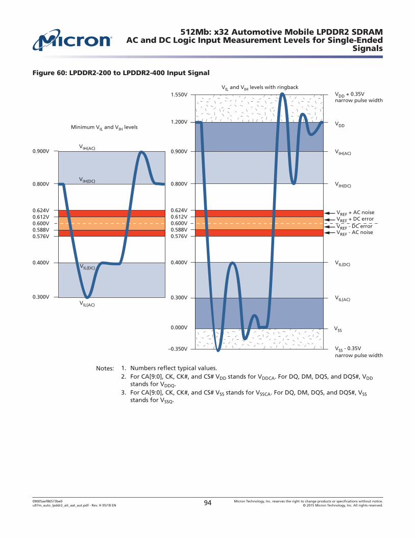
Figure 60: LPDDR2-200 to LPDDR2-400 Input Signal
0.300V
0.000V
0.400V
0.576V0.588V0.600V0.612V0.624V
0.800V
0.900V
VIL(AC)
VIL(DC)
VREF - AC noiseVREF - DC errorVREF + DC errorVREF + AC noise
VIH(DC)
VIH(AC)
1.200V
1.550V
–0.350V
VDD
VDD + 0.35Vnarrow pulse width
VSS - 0.35Vnarrow pulse width
VSS
0.300V
0.400V
0.576V0.588V0.600V0.612V0.624V
0.800V
0.900V
Minimum VIL and VIH levels
VIH(DC)
VIH(AC)
VIL(AC)
VIL(DC)
VIL and VIH levels with ringback
Notes: 1. Numbers reflect typical values.2. For CA[9:0], CK, CK#, and CS# VDD stands for VDDCA. For DQ, DM, DQS, and DQS#, VDD
stands for VDDQ.3. For CA[9:0], CK, CK#, and CS# VSS stands for VSSCA. For DQ, DM, DQS, and DQS#, VSS
stands for VSSQ.
512Mb: x32 Automotive Mobile LPDDR2 SDRAMAC and DC Logic Input Measurement Levels for Single-Ended
Signals
09005aef86573be0u97m_auto_lpddr2_ait_aat_aut.pdf - Rev. H 05/18 EN 94 Micron Technology, Inc. reserves the right to change products or specifications without notice.
© 2015 Micron Technology, Inc. All rights reserved.
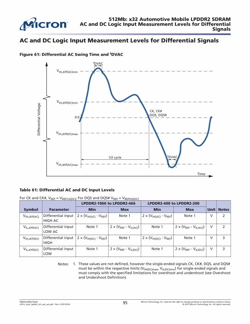
AC and DC Logic Input Measurement Levels for Differential Signals
Figure 61: Differential AC Swing Time and tDVAC
tDVAC
tDVAC1/2 cycle
Time
VIH,diff(AC)min
VIH,diff(DC)min
0.0
VIH,diff(DC)max
VIH,diff(AC)max
CK, CK#DQS, DQS#
Dif
fere
nti
al V
olt
age
Table 61: Differential AC and DC Input Levels
For CK and CK#, VREF = VREFCA(DC); For DQS and DQS# VREF = VREFDQ(DC)
Symbol Parameter
LPDDR2-1066 to LPDDR2-466 LPDDR2-400 to LPDDR2-200
Unit NotesMin Max Min Max
VIH,diff(AC) Differential inputHIGH AC
2 × (VIH(AC) - VREF) Note 1 2 × (VIH(AC) - VREF) Note 1 V 2
VIL,diff(AC) Differential inputLOW AC
Note 1 2 × (VREF - VIL(AC)) Note 1 2 × (VREF - VIL(AC)) V 2
VIH,diff(DC) Differential inputHIGH
2 × (VIH(DC) - VREF) Note 1 2 × (VIH(DC) - VREF) Note 1 V 3
VIL,diff(DC) Differential inputLOW
Note 1 2 × (VREF - VIL(DC)) Note 1 2 × (VREF - VIL(DC)) V 3
Notes: 1. These values are not defined, however the single-ended signals CK, CK#, DQS, and DQS#must be within the respective limits (VIH(DC)max, VIL(DC)min) for single-ended signals andmust comply with the specified limitations for overshoot and undershoot (see Overshootand Undershoot Definition).
512Mb: x32 Automotive Mobile LPDDR2 SDRAMAC and DC Logic Input Measurement Levels for Differential
Signals
09005aef86573be0u97m_auto_lpddr2_ait_aat_aut.pdf - Rev. H 05/18 EN 95 Micron Technology, Inc. reserves the right to change products or specifications without notice.
© 2015 Micron Technology, Inc. All rights reserved.
2. For CK and CK#, use VIH/VIL(AC) of CA and VREFCA; for DQS and DQS#, use VIH/VIL(AC) of DQand VREFDQ. If a reduced AC HIGH or AC LOW is used for a signal group, the reducedvoltage level also applies.
3. Used to define a differential signal slew rate.
Table 62: CK/CK# and DQS/DQS# Time Requirements Before Ringback(tDVAC)
Slew Rate (V/ns)
tDVAC (ps) at VIH/VILdiff(AC) =440mV
tDVAC (ps) at VIH/VILdiff(AC) =600mV
Min Min
> 4.0 175 75
4.0 170 57
3.0 167 50
2.0 163 38
1.8 162 34
1.6 161 29
1.4 159 22
1.2 155 13
1.0 150 0
< 1.0 150 0
Single-Ended Requirements for Differential Signals
Each individual component of a differential signal (CK, CK#, DQS, and DQS#) must alsocomply with certain requirements for single-ended signals.
CK and CK# must meet VSEH(AC)min/VSEL(AC)max in every half cycle. DQS, DQS# mustmeet VSEH(AC)min/VSEL(AC)max in every half cycle preceding and following a valid transi-tion.
The applicable AC levels for CA and DQ differ by speed bin.
512Mb: x32 Automotive Mobile LPDDR2 SDRAMAC and DC Logic Input Measurement Levels for Differential
Signals
09005aef86573be0u97m_auto_lpddr2_ait_aat_aut.pdf - Rev. H 05/18 EN 96 Micron Technology, Inc. reserves the right to change products or specifications without notice.
© 2015 Micron Technology, Inc. All rights reserved.
Figure 62: Single-Ended Requirements for Differential Signals
Time
VDDCA or VDDQ
VSSCA or VSSQ
VDDCA/2 or VDDQ/2
VSEH(AC)min
VSEH(AC)
VSEL(AC)max
VSEL(AC)
CK or DQS
Dif
fere
nti
al V
olt
age
Note that while CA and DQ signal requirements are referenced to VREF, the single-endedcomponents of differential signals also have a requirement with respect toVDDQ/2 for DQS, and VDDCA/2 for CK.
The transition of single-ended signals through the AC levels is used to measure setuptime. For single-ended components of differential signals, the requirement to reachVSEL(AC)max or VSEH(AC)min has no bearing on timing. This requirement does, however,add a restriction on the common mode characteristics of these signals (see "Single-Ended AC and DC Input Levels for CA and CS# Inputs" for CK/CK# single-ended re-quirements, and "Single-Ended AC and DC Input Levels for DQ and DM" for DQ andDQM single-ended requirements).
Table 63: Single-Ended Levels for CK, CK#, DQS, DQS#
Symbol Parameter
LPDDR2-1066 to LPDDR2-466 LPDDR2-400 to LPDDR2-200
Unit NotesMin Max Min Max
VSEH(AC) Single-ended HIGHlevel for strobes
(VDDQ/2) + 0.220 Note 1 (VDDQ/2) + 0.300 Note 1 V 2, 3
Single-ended HIGHlevel for CK, CK#
(VDDCA/2) + 0.220 Note 1 (VDDCA/2) + 0.300 Note 1 V 2, 3
VSEL(AC) Single-ended LOWlevel for strobes
Note 1 (VDDQ/2) - 0.220 Note 1 (VDDQ/2) – 0.300 V 2, 3
Single-ended LOWlevel for CK, CK#
Note 1 (VDDCA/2) - 0.220 Note 1 (VDDCA/2) – 0.300 V 2, 3
Notes: 1. These values are not defined, however, the single-ended signals CK, CK#, DQS0, DQS#0,DQS1, DQS#1, DQS2, DQS#2, DQS3, DQS#3 must be within the respective limits(VIH(DC)max/ VIL(DC)min) for single-ended signals, and must comply with the specified limi-tations for overshoot and undershoot (See Overshoot and Undershoot Definition).
512Mb: x32 Automotive Mobile LPDDR2 SDRAMAC and DC Logic Input Measurement Levels for Differential
Signals
09005aef86573be0u97m_auto_lpddr2_ait_aat_aut.pdf - Rev. H 05/18 EN 97 Micron Technology, Inc. reserves the right to change products or specifications without notice.
© 2015 Micron Technology, Inc. All rights reserved.
2. For CK and CK#, use VSEH/VSEL(AC) of CA; for strobes (DQS[3:0] and DQS#[3:0]), useVIH/VIL(AC) of DQ.
3. VIH(AC) and VIL(AC) for DQ are based on VREFDQ; VSEH(AC) and VSEL(AC) for CA are based onVREFCA. If a reduced AC HIGH or AC LOW is used for a signal group, the reduced levelapplies.
Differential Input Crosspoint Voltage
To ensure tight setup and hold times as well as output skew parameters with respect toclock and strobe, each crosspoint voltage of differential input signals (CK, CK#, DQS,and DQS#) must meet the specifications in Table 63 (page 97). The differential inputcrosspoint voltage (VIX) is measured from the actual crosspoint of the true signal and itsand complement to the midlevel between VDD and VSS.
Figure 63: VIX Definition
VDDCA, VDDQ
VSSCA, VSSQ
VDDCA/2,
VDDQ/2VDDCA/2,
VDDQ/2
CK#, DQS#
VIX
CK, DQS
VDDCA, VDDQ
VSSCA, VSSQ
CK#, DQS#
VIX
VIX
CK, DQS
VIX
X
X X
X
Table 64: Crosspoint Voltage for Differential Input Signals (CK, CK#, DQS, DQS#)
Symbol Parameter
LPDDR2-1066 to LPDDR2-200
Unit NotesMin Max
VIXCA(AC) Differential input crosspoint voltage rela-tive to VDDCA/2 for CK and CK#
–120 120 mV 1, 2
VIXDQ(AC) Differential input crosspoint voltage rela-tive to VDDQ/2 for DQS and DQ#
–120 120 mV 1, 2
Notes: 1. The typical value of VIX(AC) is expected to be about 0.5 × VDD of the transmitting device,and it is expected to track variations in VDD. VIX(AC) indicates the voltage at which differ-ential input signals must cross.
2. For CK and CK#, VREF = VREFCA(DC). For DQS and DQS#, VREF = VREFDQ(DC).
512Mb: x32 Automotive Mobile LPDDR2 SDRAMAC and DC Logic Input Measurement Levels for Differential
Signals
09005aef86573be0u97m_auto_lpddr2_ait_aat_aut.pdf - Rev. H 05/18 EN 98 Micron Technology, Inc. reserves the right to change products or specifications without notice.
© 2015 Micron Technology, Inc. All rights reserved.
Input Slew Rate
Table 65: Differential Input Slew Rate Definition
Description
Measured1
Defined byFrom To
Differential input slew rate for risingedge (CK/CK# and DQS/DQS#)
VIL,diff,max VIH,diff,min [VIH,diff,min - VIL,diff,maxΔTRdiff
Differential input slew rate for fallingedge (CK/CK# and DQS/DQS#)
VIH,diff,min VIL,diff,max [VIH,diff,min - VIL,diff,maxΔTFdiff
Note: 1. The differential signals (CK/CK# and DQS/DQS#) must be linear between these thresh-olds.
Figure 64: Differential Input Slew Rate Definition for CK, CK#, DQS, and DQS#
VIH,diff,min
0
VIL,diff,max
Time
Dif
fere
nti
al In
pu
t V
olt
age
TFdiff TRdiff
Output Characteristics and Operating Conditions
Table 66: Single-Ended AC and DC Output Levels
Symbol Parameter Value Unit Notes
VOH(AC) AC output HIGH measurement level (for output slew rate) VREF + 0.12 V
VOL(AC) AC output LOW measurement level (for output slew rate) VREF - 0.12 V
VOH(DC) DC output HIGH measurement level (for I-V curve linearity) 0.9 x VDDQ V 1
VOL(DC) DC output LOW measurement level (for I-V curve linearity) 0.1 x VDDQ V 2
IOZ Output leakage current (DQ, DM, DQS, DQS#); DQ,DQS, DQS# are disabled; 0V ≤ VOUT ≤ VDDQ
MIN –5 μA
MAX +5 μA
MMpupd Delta output impedance between pull-up and pull-down for DQ/DM
MIN –15 %
MAX +15 %
Notes: 1. IOH = –0.1mA.2. IOL = 0.1mA.
512Mb: x32 Automotive Mobile LPDDR2 SDRAMOutput Characteristics and Operating Conditions
09005aef86573be0u97m_auto_lpddr2_ait_aat_aut.pdf - Rev. H 05/18 EN 99 Micron Technology, Inc. reserves the right to change products or specifications without notice.
© 2015 Micron Technology, Inc. All rights reserved.
Table 67: Differential AC and DC Output Levels
Symbol Parameter Value Unit
VOHdiff(AC) AC differential output HIGH measurement level (for output SR) + 0.2 x VDDQ V
VOLdiff(AC) AC differential output LOW measurement level (for output SR) - 0.2 x VDDQ V
Single-Ended Output Slew Rate
With the reference load for timing measurements, the output slew rate for falling andrising edges is defined and measured between VOL(AC) and VOH(AC) for single-endedsignals.
Table 68: Single-Ended Output Slew Rate Definition
Description
Measured
Defined byFrom To
Single-ended output slew rate for rising edge VOL(AC) VOH(AC) [VOH(AC) - VOL(AC)ΔTRSE
Single-ended output slew rate for falling edge VOH(AC) VOL(AC) [VOH(AC) - VOL(AC)ΔTFSE
Note: 1. Output slew rate is verified by design and characterization and may not be subject toproduction testing.
Figure 65: Single-Ended Output Slew Rate Definition
VOH(AC)
VREF
VOL(AC)
Time
Sin
gle
-En
ded
Ou
tpu
t V
olt
age
(DQ
)
TFSE TRSE
Table 69: Single-Ended Output Slew Rate
Notes 1–5 apply to all parameters conditions
Parameter Symbol
Value
UnitMin Max
Single-ended output slew rate (output impedance = 40Ω SRQSE 1.5 3.5 V/ns
Single-ended output slew rate (output impedance = 60Ω SRQSE 1.0 2.5 V/ns
512Mb: x32 Automotive Mobile LPDDR2 SDRAMOutput Characteristics and Operating Conditions
09005aef86573be0u97m_auto_lpddr2_ait_aat_aut.pdf - Rev. H 05/18 EN 100 Micron Technology, Inc. reserves the right to change products or specifications without notice.
© 2015 Micron Technology, Inc. All rights reserved.
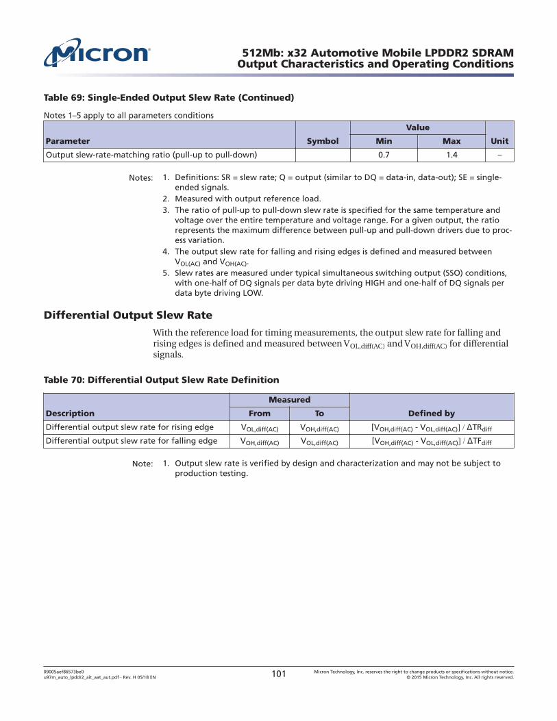
Table 69: Single-Ended Output Slew Rate (Continued)
Notes 1–5 apply to all parameters conditions
Parameter Symbol
Value
UnitMin Max
Output slew-rate-matching ratio (pull-up to pull-down) 0.7 1.4 –
Notes: 1. Definitions: SR = slew rate; Q = output (similar to DQ = data-in, data-out); SE = single-ended signals.
2. Measured with output reference load.3. The ratio of pull-up to pull-down slew rate is specified for the same temperature and
voltage over the entire temperature and voltage range. For a given output, the ratiorepresents the maximum difference between pull-up and pull-down drivers due to proc-ess variation.
4. The output slew rate for falling and rising edges is defined and measured betweenVOL(AC) and VOH(AC).
5. Slew rates are measured under typical simultaneous switching output (SSO) conditions,with one-half of DQ signals per data byte driving HIGH and one-half of DQ signals perdata byte driving LOW.
Differential Output Slew Rate
With the reference load for timing measurements, the output slew rate for falling andrising edges is defined and measured between VOL,diff(AC) and VOH,diff(AC) for differentialsignals.
Table 70: Differential Output Slew Rate Definition
Description
Measured
Defined byFrom To
Differential output slew rate for rising edge VOL,diff(AC) VOH,diff(AC) [VOH,diff(AC) - VOL,diff(AC)ΔTRdiff
Differential output slew rate for falling edge VOH,diff(AC) VOL,diff(AC) [VOH,diff(AC) - VOL,diff(AC)ΔTFdiff
Note: 1. Output slew rate is verified by design and characterization and may not be subject toproduction testing.
512Mb: x32 Automotive Mobile LPDDR2 SDRAMOutput Characteristics and Operating Conditions
09005aef86573be0u97m_auto_lpddr2_ait_aat_aut.pdf - Rev. H 05/18 EN 101 Micron Technology, Inc. reserves the right to change products or specifications without notice.
© 2015 Micron Technology, Inc. All rights reserved.
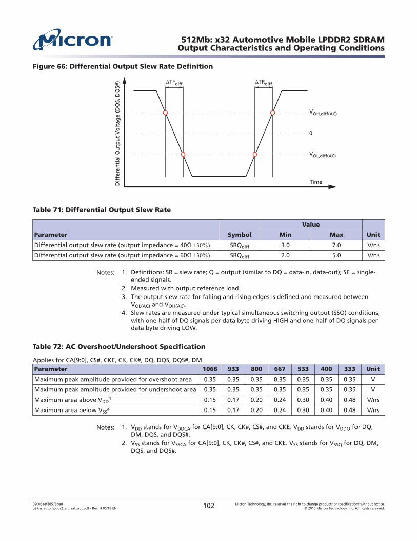
Figure 66: Differential Output Slew Rate Definition
VOH,diff(AC)
0
VOL,diff(AC)
TimeDif
fere
nti
al O
utp
ut
Vo
ltag
e (D
QS,
DQ
S#) TFdiff TRdiff
Table 71: Differential Output Slew Rate
Parameter Symbol
Value
UnitMin Max
Differential output slew rate (output impedance = 40Ω SRQdiff 3.0 7.0 V/ns
Differential output slew rate (output impedance = 60Ω SRQdiff 2.0 5.0 V/ns
Notes: 1. Definitions: SR = slew rate; Q = output (similar to DQ = data-in, data-out); SE = single-ended signals.
2. Measured with output reference load.3. The output slew rate for falling and rising edges is defined and measured between
VOL(AC) and VOH(AC).4. Slew rates are measured under typical simultaneous switching output (SSO) conditions,
with one-half of DQ signals per data byte driving HIGH and one-half of DQ signals perdata byte driving LOW.
Table 72: AC Overshoot/Undershoot Specification
Applies for CA[9:0], CS#, CKE, CK, CK#, DQ, DQS, DQS#, DMParameter 1066 933 800 667 533 400 333 Unit
Maximum peak amplitude provided for overshoot area 0.35 0.35 0.35 0.35 0.35 0.35 0.35 V
Maximum peak amplitude provided for undershoot area 0.35 0.35 0.35 0.35 0.35 0.35 0.35 V
Maximum area above VDD1 0.15 0.17 0.20 0.24 0.30 0.40 0.48 V/ns
Maximum area below VSS2 0.15 0.17 0.20 0.24 0.30 0.40 0.48 V/ns
Notes: 1. VDD stands for VDDCA for CA[9:0], CK, CK#, CS#, and CKE. VDD stands for VDDQ for DQ,DM, DQS, and DQS#.
2. VSS stands for VSSCA for CA[9:0], CK, CK#, CS#, and CKE. VSS stands for VSSQ for DQ, DM,DQS, and DQS#.
512Mb: x32 Automotive Mobile LPDDR2 SDRAMOutput Characteristics and Operating Conditions
09005aef86573be0u97m_auto_lpddr2_ait_aat_aut.pdf - Rev. H 05/18 EN 102 Micron Technology, Inc. reserves the right to change products or specifications without notice.
© 2015 Micron Technology, Inc. All rights reserved.
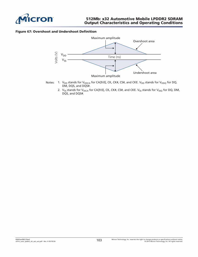
Figure 67: Overshoot and Undershoot Definition
Overshoot area
VDD
VSSVol
ts (V
)
Undershoot area
Maximum amplitude
Maximum amplitude
Time (ns)
Notes: 1. VDD stands for VDDCA for CA[9:0], CK, CK#, CS#, and CKE. VDD stands for VDDQ for DQ,DM, DQS, and DQS#.
2. VSS stands for VSSCA for CA[9:0], CK, CK#, CS#, and CKE. VSS stands for VSSQ for DQ, DM,DQS, and DQS#.
512Mb: x32 Automotive Mobile LPDDR2 SDRAMOutput Characteristics and Operating Conditions
09005aef86573be0u97m_auto_lpddr2_ait_aat_aut.pdf - Rev. H 05/18 EN 103 Micron Technology, Inc. reserves the right to change products or specifications without notice.
© 2015 Micron Technology, Inc. All rights reserved.
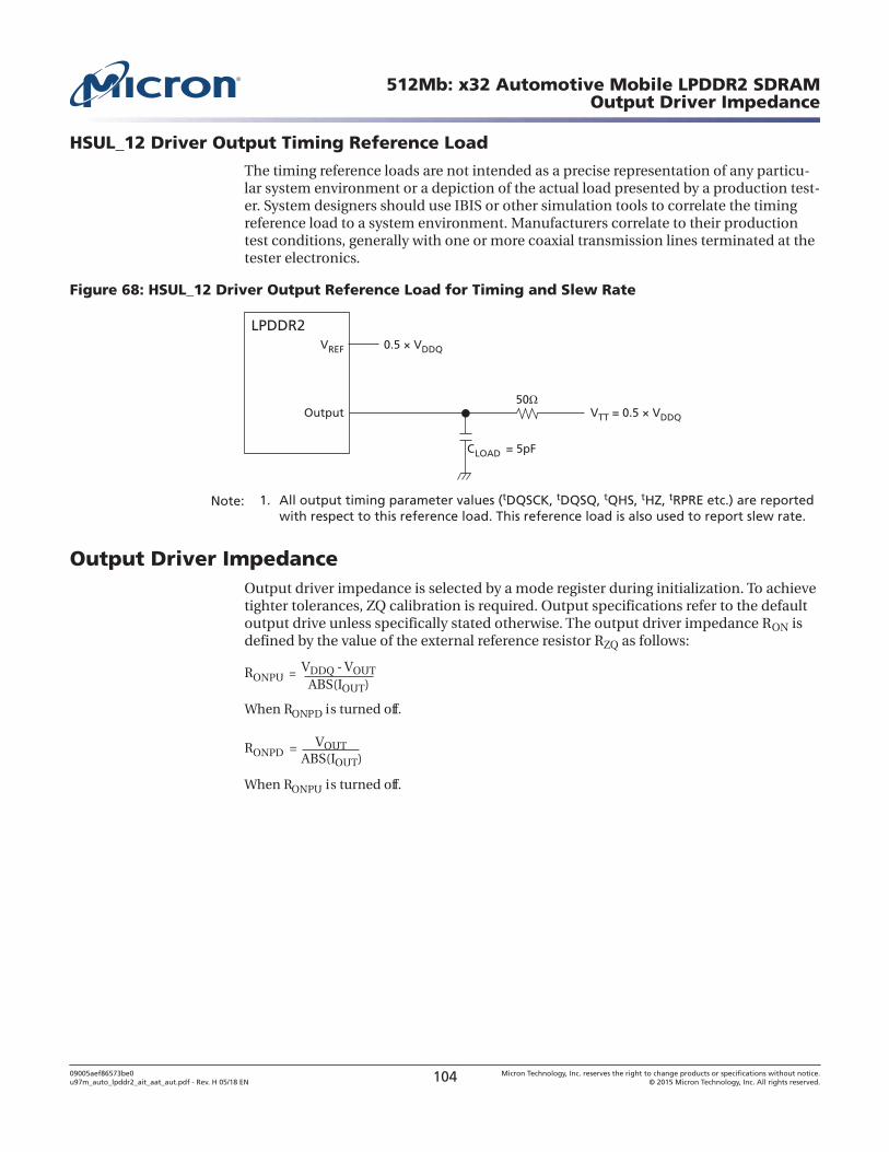
HSUL_12 Driver Output Timing Reference Load
The timing reference loads are not intended as a precise representation of any particu-lar system environment or a depiction of the actual load presented by a production test-er. System designers should use IBIS or other simulation tools to correlate the timingreference load to a system environment. Manufacturers correlate to their productiontest conditions, generally with one or more coaxial transmission lines terminated at thetester electronics.
Figure 68: HSUL_12 Driver Output Reference Load for Timing and Slew Rate
LPDDR2VREF 0.5 × VDDQ
Output
CLOAD = 5pF
VTT = 0.5 × VDDQ
50
Note: 1. All output timing parameter values (tDQSCK, tDQSQ, tQHS, tHZ, tRPRE etc.) are reportedwith respect to this reference load. This reference load is also used to report slew rate.
Output Driver ImpedanceOutput driver impedance is selected by a mode register during initialization. To achievetighter tolerances, ZQ calibration is required. Output specifications refer to the defaultoutput drive unless specifically stated otherwise. The output driver impedance RON isdefined by the value of the external reference resistor RZQ as follows:
RONPU = VDDQ - VOUT ABS(IOUT)
When RONPD is turned off.
RONPD = VOUT
When RONPU is turned off.
ABS(IOUT)
512Mb: x32 Automotive Mobile LPDDR2 SDRAMOutput Driver Impedance
09005aef86573be0u97m_auto_lpddr2_ait_aat_aut.pdf - Rev. H 05/18 EN 104 Micron Technology, Inc. reserves the right to change products or specifications without notice.
© 2015 Micron Technology, Inc. All rights reserved.
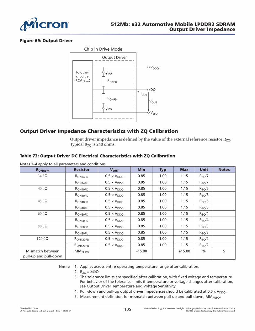
Figure 69: Output Driver
To othercircuitry
(RCV, etc.)
Output Driver
Chip in Drive Mode
IPU
RONPU
RONPD
IPD
IOUT
VDDQ
VOUT
DQ
VSSQ
Output Driver Impedance Characteristics with ZQ Calibration
Output driver impedance is defined by the value of the external reference resistor RZQ.Typical RZQ is 240 ohms.
Table 73: Output Driver DC Electrical Characteristics with ZQ Calibration
Notes 1–4 apply to all parameters and conditionsRONnom Resistor VOUT Min Typ Max Unit Notes
Ω RON34PD 0.5 × VDDQ 0.85 1.00 1.15 RZQ/7
RON34PU 0.5 × VDDQ 0.85 1.00 1.15 RZQ/7
Ω RON40PD 0.5 × VDDQ 0.85 1.00 1.15 RZQ/6
RON40PU 0.5 × VDDQ 0.85 1.00 1.15 RZQ/6
Ω RON48PD 0.5 × VDDQ 0.85 1.00 1.15 RZQ/5
RON48PU 0.5 × VDDQ 0.85 1.00 1.15 RZQ/5
Ω RON60PD 0.5 × VDDQ 0.85 1.00 1.15 RZQ/4
RON60PU 0.5 × VDDQ 0.85 1.00 1.15 RZQ/4
Ω RON80PD 0.5 × VDDQ 0.85 1.00 1.15 RZQ/3
RON80PU 0.5 × VDDQ 0.85 1.00 1.15 RZQ/3
Ω RON120PD 0.5 × VDDQ 0.85 1.00 1.15 RZQ/2
RON120PU 0.5 × VDDQ 0.85 1.00 1.15 RZQ/2
Mismatch betweenpull-up and pull-down
MMPUPD –15.00 +15.00 % 5
Notes: 1. Applies across entire operating temperature range after calibration.2. RZQ Ω3. The tolerance limits are specified after calibration, with fixed voltage and temperature.
For behavior of the tolerance limits if temperature or voltage changes after calibration,see Output Driver Temperature and Voltage Sensitivity.
4. Pull-down and pull-up output driver impedances should be calibrated at 0.5 x VDDQ.5. Measurement definition for mismatch between pull-up and pull-down, MMPUPD:
512Mb: x32 Automotive Mobile LPDDR2 SDRAMOutput Driver Impedance
09005aef86573be0u97m_auto_lpddr2_ait_aat_aut.pdf - Rev. H 05/18 EN 105 Micron Technology, Inc. reserves the right to change products or specifications without notice.
© 2015 Micron Technology, Inc. All rights reserved.
Measure RONPU and RONPD, both at 0.5 × VDDQ:
MMPUPD = RONPU – RONPD × 100 RON,nom
For example, with MMPUPD (MAX) = 15% and RONPD = 0.85, RONPU must be less than 1.0.
Output Driver Temperature and Voltage Sensitivity
If temperature and/or voltage change after calibration, the tolerance limits widen.
Table 74: Output Driver Sensitivity Definition
Resistor VOUT Min Max Unit
RONPD 0.5 × VDDQ 85 – (dRONdT ΔT|) – (dRONdV ΔV|) 115 + (dRONdT ΔT|) – (dRONdV ΔV|) %
RONPU
Notes: 1. ΔT = T - T (at calibration). ΔV = V - V (at calibration).2. dRONdT and dRONdV are not subject to production testing; they are verified by design
and characterization.
Table 75: Output Driver Temperature and Voltage Sensitivity
Symbol Parameter Min Max Unit
RONdT RON temperature sensitivity 0.00 0.75 %/˚C
RONdV RON voltage sensitivity 0.00 0.20 %/mV
Output Impedance Characteristics Without ZQ Calibration
Output driver impedance is defined by design and characterization as the default set-ting.
Table 76: Output Driver DC Electrical Characteristics Without ZQ Calibration
RONnom Resistor VOUT Min Typ Max Unit
Ω RON34PD 0.5 × VDDQ 0.70 1.00 1.30 RZQ/7
RON34PU 0.5 × VDDQ 0.70 1.00 1.30 RZQ/7
Ω RON40PD 0.5 × VDDQ 0.70 1.00 1.30 RZQ/6
RON40PU 0.5 × VDDQ 0.70 1.00 1.30 RZQ/6
Ω RON48PD 0.5 × VDDQ 0.70 1.00 1.30 RZQ/5
RON48PU 0.5 × VDDQ 0.70 1.00 1.30 RZQ/5
Ω RON60PD 0.5 × VDDQ 0.70 1.00 1.30 RZQ/4
RON60PU 0.5 × VDDQ 0.70 1.00 1.30 RZQ/4
Ω RON80PD 0.5 × VDDQ 0.70 1.00 1.30 RZQ/3
RON80PU 0.5 × VDDQ 0.70 1.00 1.30 RZQ/3
512Mb: x32 Automotive Mobile LPDDR2 SDRAMOutput Driver Impedance
09005aef86573be0u97m_auto_lpddr2_ait_aat_aut.pdf - Rev. H 05/18 EN 106 Micron Technology, Inc. reserves the right to change products or specifications without notice.
© 2015 Micron Technology, Inc. All rights reserved.
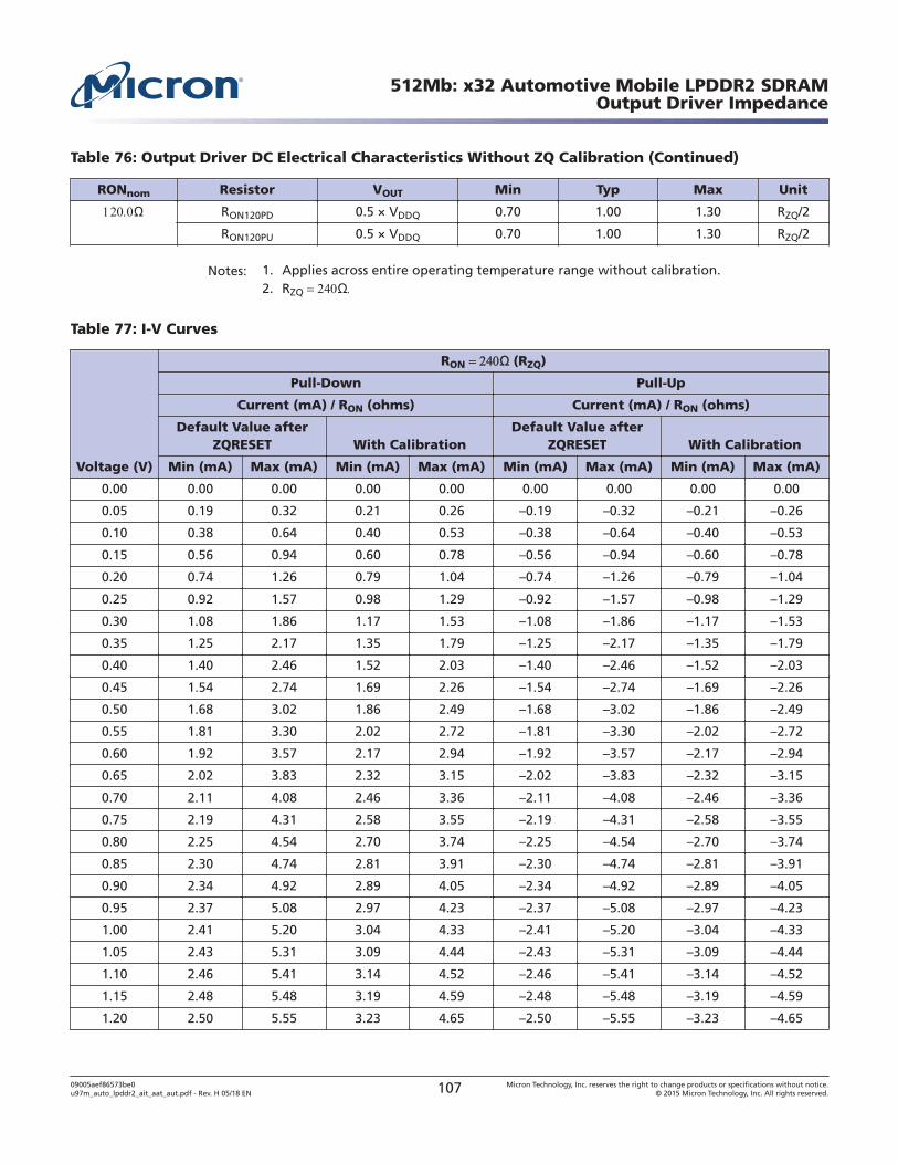
Table 76: Output Driver DC Electrical Characteristics Without ZQ Calibration (Continued)
RONnom Resistor VOUT Min Typ Max Unit
Ω RON120PD 0.5 × VDDQ 0.70 1.00 1.30 RZQ/2
RON120PU 0.5 × VDDQ 0.70 1.00 1.30 RZQ/2
Notes: 1. Applies across entire operating temperature range without calibration.2. RZQ Ω
Table 77: I-V Curves
Voltage (V)
RON Ω (RZQ)
Pull-Down Pull-Up
Current (mA) / RON (ohms) Current (mA) / RON (ohms)
Default Value afterZQRESET With Calibration
Default Value afterZQRESET With Calibration
Min (mA) Max (mA) Min (mA) Max (mA) Min (mA) Max (mA) Min (mA) Max (mA)
0.00 0.00 0.00 0.00 0.00 0.00 0.00 0.00 0.00
0.05 0.19 0.32 0.21 0.26 –0.19 –0.32 –0.21 –0.26
0.10 0.38 0.64 0.40 0.53 –0.38 –0.64 –0.40 –0.53
0.15 0.56 0.94 0.60 0.78 –0.56 –0.94 –0.60 –0.78
0.20 0.74 1.26 0.79 1.04 –0.74 –1.26 –0.79 –1.04
0.25 0.92 1.57 0.98 1.29 –0.92 –1.57 –0.98 –1.29
0.30 1.08 1.86 1.17 1.53 –1.08 –1.86 –1.17 –1.53
0.35 1.25 2.17 1.35 1.79 –1.25 –2.17 –1.35 –1.79
0.40 1.40 2.46 1.52 2.03 –1.40 –2.46 –1.52 –2.03
0.45 1.54 2.74 1.69 2.26 –1.54 –2.74 –1.69 –2.26
0.50 1.68 3.02 1.86 2.49 –1.68 –3.02 –1.86 –2.49
0.55 1.81 3.30 2.02 2.72 –1.81 –3.30 –2.02 –2.72
0.60 1.92 3.57 2.17 2.94 –1.92 –3.57 –2.17 –2.94
0.65 2.02 3.83 2.32 3.15 –2.02 –3.83 –2.32 –3.15
0.70 2.11 4.08 2.46 3.36 –2.11 –4.08 –2.46 –3.36
0.75 2.19 4.31 2.58 3.55 –2.19 –4.31 –2.58 –3.55
0.80 2.25 4.54 2.70 3.74 –2.25 –4.54 –2.70 –3.74
0.85 2.30 4.74 2.81 3.91 –2.30 –4.74 –2.81 –3.91
0.90 2.34 4.92 2.89 4.05 –2.34 –4.92 –2.89 –4.05
0.95 2.37 5.08 2.97 4.23 –2.37 –5.08 –2.97 –4.23
1.00 2.41 5.20 3.04 4.33 –2.41 –5.20 –3.04 –4.33
1.05 2.43 5.31 3.09 4.44 –2.43 –5.31 –3.09 –4.44
1.10 2.46 5.41 3.14 4.52 –2.46 –5.41 –3.14 –4.52
1.15 2.48 5.48 3.19 4.59 –2.48 –5.48 –3.19 –4.59
1.20 2.50 5.55 3.23 4.65 –2.50 –5.55 –3.23 –4.65
512Mb: x32 Automotive Mobile LPDDR2 SDRAMOutput Driver Impedance
09005aef86573be0u97m_auto_lpddr2_ait_aat_aut.pdf - Rev. H 05/18 EN 107 Micron Technology, Inc. reserves the right to change products or specifications without notice.
© 2015 Micron Technology, Inc. All rights reserved.
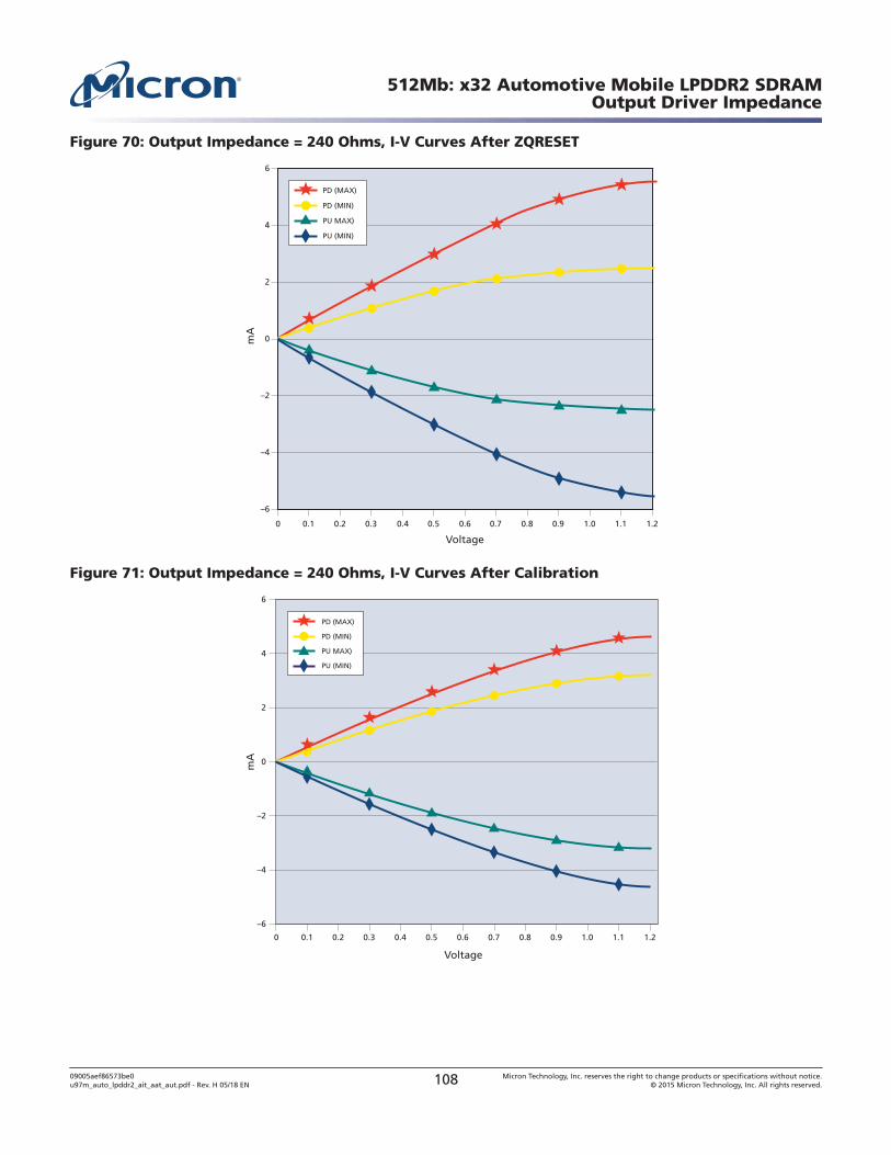
Figure 70: Output Impedance = 240 Ohms, I-V Curves After ZQRESET
6
4
2
0
–2
–4
–6
0 0.1 0.2 0.3 0.4 0.5 0.6 0.7 0.8 0.9 1.0 1.1 1.2
mA
Voltage
PD (MAX)
PD (MIN)
PU MAX)
PU (MIN)
Figure 71: Output Impedance = 240 Ohms, I-V Curves After Calibration
0 0.1 0.2 0.3 0.4 0.5 0.6 0.7 0.8 0.9 1.0 1.1 1.2
6
4
2
0
–2
–4
–6
mA
Voltage
PD (MAX)
PD (MIN)
PU MAX)
PU (MIN)
512Mb: x32 Automotive Mobile LPDDR2 SDRAMOutput Driver Impedance
09005aef86573be0u97m_auto_lpddr2_ait_aat_aut.pdf - Rev. H 05/18 EN 108 Micron Technology, Inc. reserves the right to change products or specifications without notice.
© 2015 Micron Technology, Inc. All rights reserved.
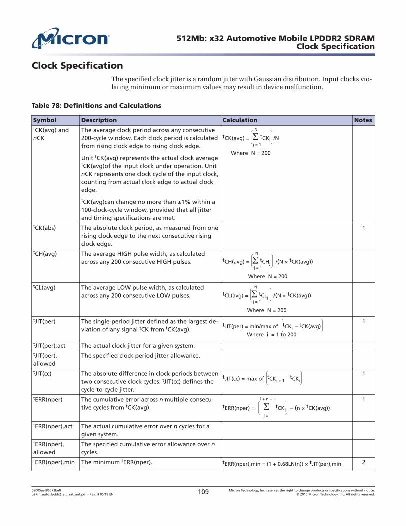
Clock SpecificationThe specified clock jitter is a random jitter with Gaussian distribution. Input clocks vio-lating minimum or maximum values may result in device malfunction.
Table 78: Definitions and Calculations
Symbol Description Calculation NotestCK(avg) andnCK
The average clock period across any consecutive200-cycle window. Each clock period is calculatedfrom rising clock edge to rising clock edge.
Unit tCK(avg) represents the actual clock averagetCK(avg)of the input clock under operation. UnitnCK represents one clock cycle of the input clock,counting from actual clock edge to actual clockedge.
tCK(avg)can change no more than ±1% within a100-clock-cycle window, provided that all jitterand timing specifications are met.
tCK(avg) = tCKj /N
Where N = 200
N
j = 1
tCK(abs) The absolute clock period, as measured from onerising clock edge to the next consecutive risingclock edge.
1
tCH(avg) The average HIGH pulse width, as calculatedacross any 200 consecutive HIGH pulses. tCH(avg) = tCHj /(N × tCK(avg))
Where N = 200
N
j = 1
tCL(avg) The average LOW pulse width, as calculatedacross any 200 consecutive LOW pulses. tCL(avg) = tCLj /(N × tCK(avg))
Where N = 200
N
j = 1
tJIT(per) The single-period jitter defined as the largest de-viation of any signal tCK from tCK(avg).
tJIT(per) = min/max of tCKi – tCK(avg)
Where i = 1 to 200
1
tJIT(per),act The actual clock jitter for a given system. tJIT(per),allowed
The specified clock period jitter allowance.
tJIT(cc) The absolute difference in clock periods betweentwo consecutive clock cycles. tJIT(cc) defines thecycle-to-cycle jitter.
tJIT(cc) = max of tCKi + 1 – tCKi
1
tERR(nper) The cumulative error across n multiple consecu-tive cycles from tCK(avg). tERR(nper) = tCKj – (n × tCK(avg))
i + n – 1
j = i
1
tERR(nper),act The actual cumulative error over n cycles for agiven system.
tERR(nper),allowed
The specified cumulative error allowance over ncycles.
tERR(nper),min The minimum tERR(nper). tERR(nper),min = (1 + 0.68LN(n)) × tJIT(per),min 2
512Mb: x32 Automotive Mobile LPDDR2 SDRAMClock Specification
09005aef86573be0u97m_auto_lpddr2_ait_aat_aut.pdf - Rev. H 05/18 EN 109 Micron Technology, Inc. reserves the right to change products or specifications without notice.
© 2015 Micron Technology, Inc. All rights reserved.
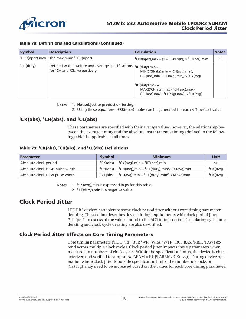
Table 78: Definitions and Calculations (Continued)
Symbol Description Calculation NotestERR(nper),max The maximum tERR(nper). tERR(nper),max = (1 + 0.68LN(n)) × tJIT(per),max 2
tJIT(duty) Defined with absolute and average specificationsfor tCH and tCL, respectively.
tJIT(duty),min = MIN((tCH(abs),min – tCH(avg),min), (tCL(abs),min – tCL(avg),min)) × tCK(avg) tJIT(duty),max = MAX((tCH(abs),max – tCH(avg),max), (tCL(abs),max – tCL(avg),max)) × tCK(avg)
Notes: 1. Not subject to production testing.2. Using these equations, tERR(nper) tables can be generated for each tJIT(per),act value.
tCK(abs), tCH(abs), and tCL(abs)
These parameters are specified with their average values; however, the relationship be-tween the average timing and the absolute instantaneous timing (defined in the follow-ing table) is applicable at all times.
Table 79: tCK(abs), tCH(abs), and tCL(abs) Definitions
Parameter Symbol Minimum Unit
Absolute clock period tCK(abs) tCK(avg),min + tJIT(per),min ps1
Absolute clock HIGH pulse width tCH(abs) tCH(avg),min + tJIT(duty),min2/tCK(avg)min tCK(avg)
Absolute clock LOW pulse width tCL(abs) tCL(avg),min + tJIT(duty),min2/tCK(avg)min tCK(avg)
Notes: 1. tCK(avg),min is expressed in ps for this table.2. tJIT(duty),min is a negative value.
Clock Period JitterLPDDR2 devices can tolerate some clock period jitter without core timing parameterderating. This section describes device timing requirements with clock period jitter(tJIT(per)) in excess of the values found in the AC Timing section. Calculating cycle timederating and clock cycle derating are also described.
Clock Period Jitter Effects on Core Timing Parameters
Core timing parameters (tRCD, tRP, tRTP, tWR, tWRA, tWTR, tRC, tRAS, tRRD, tFAW) ex-tend across multiple clock cycles. Clock period jitter impacts these parameters whenmeasured in numbers of clock cycles. Within the specification limits, the device is char-acterized and verified to support tnPARAM = RU[tPARAM/tCK(avg)]. During device op-eration where clock jitter is outside specification limits, the number of clocks ortCK(avg), may need to be increased based on the values for each core timing parameter.
512Mb: x32 Automotive Mobile LPDDR2 SDRAMClock Period Jitter
09005aef86573be0u97m_auto_lpddr2_ait_aat_aut.pdf - Rev. H 05/18 EN 110 Micron Technology, Inc. reserves the right to change products or specifications without notice.
© 2015 Micron Technology, Inc. All rights reserved.
Cycle Time Derating for Core Timing Parameters
For a given number of clocks (tnPARAM), when tCK(avg) and tERR(tnPARAM),act exceedtERR(tnPARAM),allowed, cycle time derating may be required for core timing parame-ters.
CycleTimeDerating = max tPARAM + tERR(tnPARAM),act – tERR(tnPARAM),allowed – tCK(avg) , 0
tnPARAM
Cycle time derating analysis should be conducted for each core timing parameter. Theamount of cycle time derating required is the maximum of the cycle time deratings de-termined for each individual core timing parameter.
Clock Cycle Derating for Core Timing Parameters
For each core timing parameter and a given number of clocks (tnPARAM), clock cyclederating should be specified with tJIT(per).
For a given number of clocks (tnPARAM), when tCK(avg) plus (tERR(tnPARAM),act) ex-ceed the supported cumulative tERR(tnPARAM),allowed, derating is required. If theequation below results in a positive value for a core timing parameter (tCORE), the re-quired clock cycle derating will be that positive value (in clocks).
ClockCycleDerating = RU tPARAM + tERR(tnPARAM),act – tERR(tnPARAM),allowed – tnPARAM
tCK(avg)
Cycle-time derating analysis should be conducted for each core timing parameter.
Clock Jitter Effects on Command/Address Timing Parameters
Command/address timing parameters (tIS, tIH, tISCKE, tIHCKE, tISb, tIHb, tISCKEb,tIHCKEb) are measured from a command/address signal (CKE, CS, or CA[9:0]) transi-tion edge to its respective clock signal (CK/CK#) crossing. The specification values arenot affected by the tJIT(per) applied, because the setup and hold times are relative tothe clock signal crossing that latches the command/address. Regardless of clock jittervalues, these values must be met.
Clock Jitter Effects on READ Timing ParameterstRPRE
When the device is operated with input clock jitter, tRPRE must be derated by thetJIT(per),act,max of the input clock that exceeds tJIT(per),allowed,max. Output derat-ings are relative to the input clock:
tRPRE(min,derated) = 0.9 – tJIT(per),act,max – tJIT(per),allowed,max
tCK(avg)
For example, if the measured jitter into a LPDDR2-800 device has tCK(avg) = 2500ps,tJIT(per),act,min = –172ps, and tJIT(per),act,max = +193ps, then tRPRE,min,derated =0.9 - (tJIT(per),act,max - tJIT(per),allowed,max)/tCK(avg) = 0.9 - (193 - 100)/2500 =0.8628 tCK(avg).
512Mb: x32 Automotive Mobile LPDDR2 SDRAMClock Period Jitter
09005aef86573be0u97m_auto_lpddr2_ait_aat_aut.pdf - Rev. H 05/18 EN 111 Micron Technology, Inc. reserves the right to change products or specifications without notice.
© 2015 Micron Technology, Inc. All rights reserved.
tLZ(DQ), tHZ(DQ), tDQSCK, tLZ(DQS), tHZ(DQS)
These parameters are measured from a specific clock edge to a data signal transition(DMn or DQm, where: n = 0, 1, 2, or 3; and m = DQ[31:0]), and specified timings must bemet with respect to that clock edge. Therefore, they are not affected by tJIT(per).
tQSH, tQSL
These parameters are affected by duty cycle jitter, represented by tCH(abs)min andtCL(abs)min. These parameters determine the absolute data valid window at the devicepin. The absolute minimum data valid window at the device pin = min [(tQSH(abs)min× tCK(avg)min - tDQSQmax - tQHSmax), (tQSL(abs)min × tCK(avg)min - tDQSQmax -tQHSmax)]. This minimum data valid window must be met at the target frequency re-gardless of clock jitter.
tRPST
tRPST is affected by duty cycle jitter, represented by tCL(abs). Therefore, tRPST(abs)mincan be specified by tCL(abs)min. tRPST(abs)min = tCL(abs)min - 0.05 = tQSL(abs)min.
Clock Jitter Effects on WRITE Timing ParameterstDS, tDH
These parameters are measured from a data signal (DMn or DQm, where n = 0, 1, 2, 3;and m = DQ[31:0]) transition edge to its respective data strobe signal (DQSn, DQSn#: n= 0,1,2,3) crossing. The specification values are not affected by the amount of tJIT(per)applied, because the setup and hold times are relative to the clock signal crossing thatlatches the command/address. Regardless of clock jitter values, these values must bemet.
tDSS, tDSH
These parameters are measured from a data strobe signal crossing (DQSx, DQSx#) to itsclock signal crossing (CK/CK#). The specification values are not affected by the amountof tJIT(per)) applied, because the setup and hold times are relative to the clock signalcrossing that latches the command/address. Regardless of clock jitter values, these val-ues must be met.
tDQSS
tDQSS is measured from the clock signal crossing (CK/CK#) to the first latching datastrobe signal crossing (DQSx, DQSx#). When the device is operated with input clock jit-ter, this parameter must be derated by the actual tJIT(per),act of the input clock in ex-cess of tJIT(per),allowed.
tDQSS(min,derated) = 0.75 - tJIT(per),act,min – tJIT(per),allowed, min
tCK(avg)
tDQSS(max,derated) = 1.25 – tJIT(per),act,max – tJIT(per),allowed, max
tCK(avg)
For example, if the measured jitter into an LPDDR2-800 device has tCK(avg) = 2500ps,tJIT(per),act,min = -172ps, and tJIT(per),act,max = +193ps, then:
tDQSS,(min,derated) = 0.75 - (tJIT(per),act,min - tJIT(per),allowed,min)/tCK(avg) =0.75 - (-172 + 100)/2500 = 0.7788 tCK(avg), and
tDQSS,(max,derated) = 1.25 - (tJIT(per),act,max - tJIT(per),allowed,max)/tCK(avg) =
512Mb: x32 Automotive Mobile LPDDR2 SDRAMClock Period Jitter
09005aef86573be0u97m_auto_lpddr2_ait_aat_aut.pdf - Rev. H 05/18 EN 112 Micron Technology, Inc. reserves the right to change products or specifications without notice.
© 2015 Micron Technology, Inc. All rights reserved.
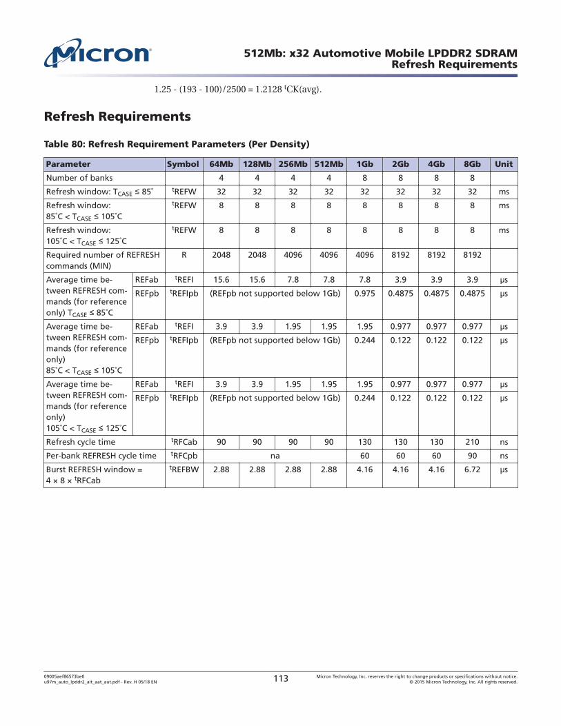
1.25 - (193 - 100)/2500 = 1.2128 tCK(avg).
Refresh Requirements
Table 80: Refresh Requirement Parameters (Per Density)
Parameter Symbol 64Mb 128Mb 256Mb 512Mb 1Gb 2Gb 4Gb 8Gb Unit
Number of banks 4 4 4 4 8 8 8 8
Refresh window: TCASE ≤ 85˚ tREFW 32 32 32 32 32 32 32 32 ms
Refresh window:85˚C < TCASE ≤ 105˚C
tREFW 8 8 8 8 8 8 8 8 ms
Refresh window:105˚C < TCASE ≤ 125˚C
tREFW 8 8 8 8 8 8 8 8 ms
Required number of REFRESHcommands (MIN)
R 2048 2048 4096 4096 4096 8192 8192 8192
Average time be-tween REFRESH com-mands (for referenceonly) TCASE ≤ 85˚C
REFab tREFI 15.6 15.6 7.8 7.8 7.8 3.9 3.9 3.9 μs
REFpb tREFIpb (REFpb not supported below 1Gb) 0.975 0.4875 0.4875 0.4875 μs
Average time be-tween REFRESH com-mands (for referenceonly)85˚C < TCASE ≤ 105˚C
REFab tREFI 3.9 3.9 1.95 1.95 1.95 0.977 0.977 0.977 μs
REFpb tREFIpb (REFpb not supported below 1Gb) 0.244 0.122 0.122 0.122 μs
Average time be-tween REFRESH com-mands (for referenceonly)105˚C < TCASE ≤ 125˚C
REFab tREFI 3.9 3.9 1.95 1.95 1.95 0.977 0.977 0.977 μs
REFpb tREFIpb (REFpb not supported below 1Gb) 0.244 0.122 0.122 0.122 μs
Refresh cycle time tRFCab 90 90 90 90 130 130 130 210 ns
Per-bank REFRESH cycle time tRFCpb na 60 60 60 90 ns
Burst REFRESH window =4 × 8 × tRFCab
tREFBW 2.88 2.88 2.88 2.88 4.16 4.16 4.16 6.72 μs
512Mb: x32 Automotive Mobile LPDDR2 SDRAMRefresh Requirements
09005aef86573be0u97m_auto_lpddr2_ait_aat_aut.pdf - Rev. H 05/18 EN 113 Micron Technology, Inc. reserves the right to change products or specifications without notice.
© 2015 Micron Technology, Inc. All rights reserved.
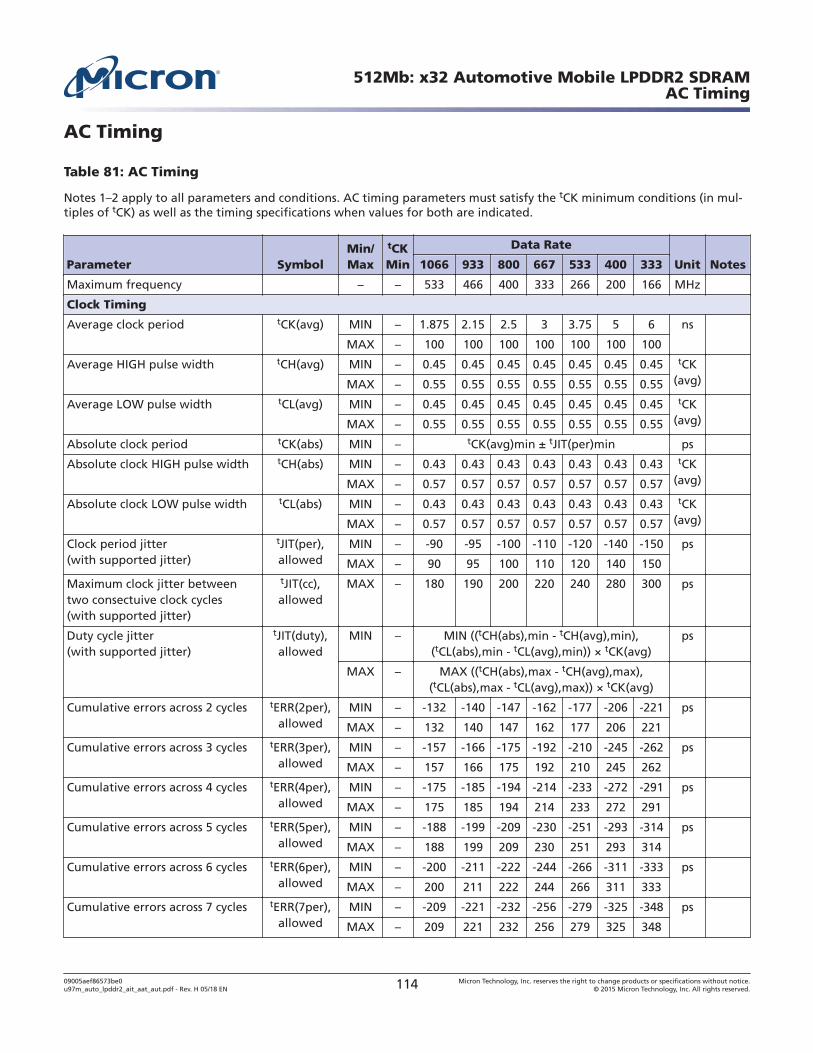
AC Timing
Table 81: AC Timing
Notes 1–2 apply to all parameters and conditions. AC timing parameters must satisfy the tCK minimum conditions (in mul-tiples of tCK) as well as the timing specifications when values for both are indicated.
Parameter SymbolMin/Max
tCKMin
Data Rate
Unit Notes1066 933 800 667 533 400 333
Maximum frequency – – 533 466 400 333 266 200 166 MHz
Clock Timing
Average clock period tCK(avg) MIN – 1.875 2.15 2.5 3 3.75 5 6 ns
MAX – 100 100 100 100 100 100 100
Average HIGH pulse width tCH(avg) MIN – 0.45 0.45 0.45 0.45 0.45 0.45 0.45 tCK(avg)
MAX – 0.55 0.55 0.55 0.55 0.55 0.55 0.55
Average LOW pulse width tCL(avg) MIN – 0.45 0.45 0.45 0.45 0.45 0.45 0.45 tCK(avg)
MAX – 0.55 0.55 0.55 0.55 0.55 0.55 0.55
Absolute clock period tCK(abs) MIN – tCK(avg)min ± tJIT(per)min ps
Absolute clock HIGH pulse width tCH(abs) MIN – 0.43 0.43 0.43 0.43 0.43 0.43 0.43 tCK(avg)
MAX – 0.57 0.57 0.57 0.57 0.57 0.57 0.57
Absolute clock LOW pulse width tCL(abs) MIN – 0.43 0.43 0.43 0.43 0.43 0.43 0.43 tCK(avg)
MAX – 0.57 0.57 0.57 0.57 0.57 0.57 0.57
Clock period jitter(with supported jitter)
tJIT(per),allowed
MIN – -90 -95 -100 -110 -120 -140 -150 ps
MAX – 90 95 100 110 120 140 150
Maximum clock jitter betweentwo consectuive clock cycles(with supported jitter)
tJIT(cc),allowed
MAX – 180 190 200 220 240 280 300 ps
Duty cycle jitter(with supported jitter)
tJIT(duty),allowed
MIN – MIN ((tCH(abs),min - tCH(avg),min),(tCL(abs),min - tCL(avg),min)) × tCK(avg)
ps
MAX – MAX ((tCH(abs),max - tCH(avg),max),(tCL(abs),max - tCL(avg),max)) × tCK(avg)
Cumulative errors across 2 cycles tERR(2per),allowed
MIN – -132 -140 -147 -162 -177 -206 -221 ps
MAX – 132 140 147 162 177 206 221
Cumulative errors across 3 cycles tERR(3per),allowed
MIN – -157 -166 -175 -192 -210 -245 -262 ps
MAX – 157 166 175 192 210 245 262
Cumulative errors across 4 cycles tERR(4per),allowed
MIN – -175 -185 -194 -214 -233 -272 -291 ps
MAX – 175 185 194 214 233 272 291
Cumulative errors across 5 cycles tERR(5per),allowed
MIN – -188 -199 -209 -230 -251 -293 -314 ps
MAX – 188 199 209 230 251 293 314
Cumulative errors across 6 cycles tERR(6per),allowed
MIN – -200 -211 -222 -244 -266 -311 -333 ps
MAX – 200 211 222 244 266 311 333
Cumulative errors across 7 cycles tERR(7per),allowed
MIN – -209 -221 -232 -256 -279 -325 -348 ps
MAX – 209 221 232 256 279 325 348
512Mb: x32 Automotive Mobile LPDDR2 SDRAMAC Timing
09005aef86573be0u97m_auto_lpddr2_ait_aat_aut.pdf - Rev. H 05/18 EN 114 Micron Technology, Inc. reserves the right to change products or specifications without notice.
© 2015 Micron Technology, Inc. All rights reserved.
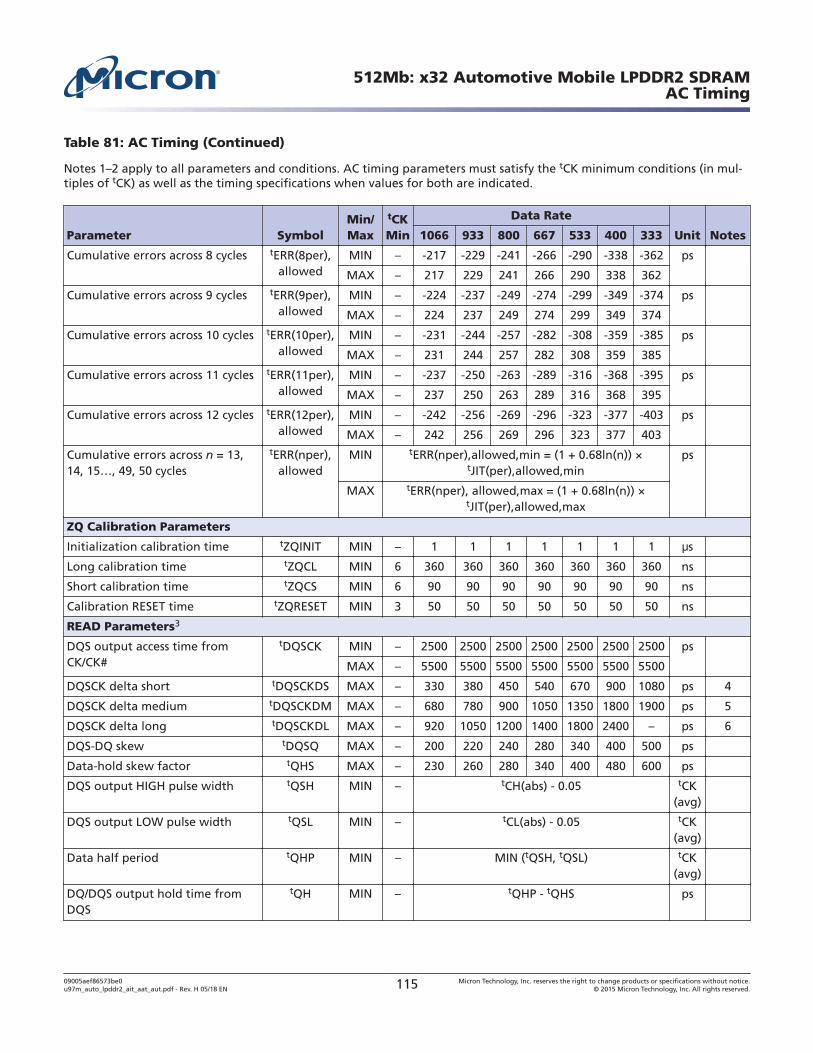
Table 81: AC Timing (Continued)
Notes 1–2 apply to all parameters and conditions. AC timing parameters must satisfy the tCK minimum conditions (in mul-tiples of tCK) as well as the timing specifications when values for both are indicated.
Parameter SymbolMin/Max
tCKMin
Data Rate
Unit Notes1066 933 800 667 533 400 333
Cumulative errors across 8 cycles tERR(8per),allowed
MIN – -217 -229 -241 -266 -290 -338 -362 ps
MAX – 217 229 241 266 290 338 362
Cumulative errors across 9 cycles tERR(9per),allowed
MIN – -224 -237 -249 -274 -299 -349 -374 ps
MAX – 224 237 249 274 299 349 374
Cumulative errors across 10 cycles tERR(10per),allowed
MIN – -231 -244 -257 -282 -308 -359 -385 ps
MAX – 231 244 257 282 308 359 385
Cumulative errors across 11 cycles tERR(11per),allowed
MIN – -237 -250 -263 -289 -316 -368 -395 ps
MAX – 237 250 263 289 316 368 395
Cumulative errors across 12 cycles tERR(12per),allowed
MIN – -242 -256 -269 -296 -323 -377 -403 ps
MAX – 242 256 269 296 323 377 403
Cumulative errors across n = 13,14, 15…, 49, 50 cycles
tERR(nper),allowed
MIN tERR(nper),allowed,min = (1 + 0.68ln(n)) ×tJIT(per),allowed,min
ps
MAX tERR(nper), allowed,max = (1 + 0.68ln(n)) ×tJIT(per),allowed,max
ZQ Calibration Parameters
Initialization calibration time tZQINIT MIN – 1 1 1 1 1 1 1 μs
Long calibration time tZQCL MIN 6 360 360 360 360 360 360 360 ns
Short calibration time tZQCS MIN 6 90 90 90 90 90 90 90 ns
Calibration RESET time tZQRESET MIN 3 50 50 50 50 50 50 50 ns
READ Parameters3
DQS output access time fromCK/CK#
tDQSCK MIN – 2500 2500 2500 2500 2500 2500 2500 ps
MAX – 5500 5500 5500 5500 5500 5500 5500
DQSCK delta short tDQSCKDS MAX – 330 380 450 540 670 900 1080 ps 4
DQSCK delta medium tDQSCKDM MAX – 680 780 900 1050 1350 1800 1900 ps 5
DQSCK delta long tDQSCKDL MAX – 920 1050 1200 1400 1800 2400 – ps 6
DQS-DQ skew tDQSQ MAX – 200 220 240 280 340 400 500 ps
Data-hold skew factor tQHS MAX – 230 260 280 340 400 480 600 ps
DQS output HIGH pulse width tQSH MIN – tCH(abs) - 0.05 tCK(avg)
DQS output LOW pulse width tQSL MIN – tCL(abs) - 0.05 tCK(avg)
Data half period tQHP MIN – MIN (tQSH, tQSL) tCK(avg)
DQ/DQS output hold time fromDQS
tQH MIN – tQHP - tQHS ps
512Mb: x32 Automotive Mobile LPDDR2 SDRAMAC Timing
09005aef86573be0u97m_auto_lpddr2_ait_aat_aut.pdf - Rev. H 05/18 EN 115 Micron Technology, Inc. reserves the right to change products or specifications without notice.
© 2015 Micron Technology, Inc. All rights reserved.
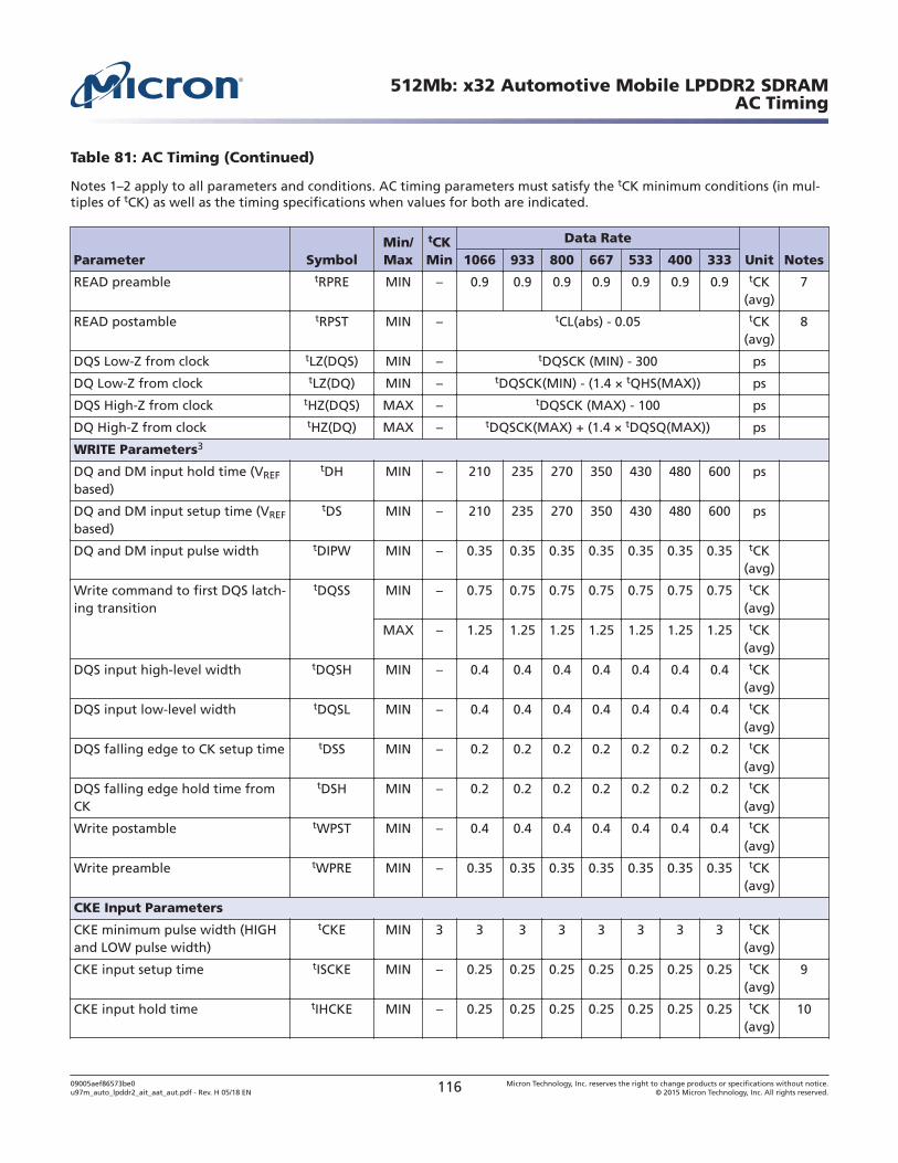
Table 81: AC Timing (Continued)
Notes 1–2 apply to all parameters and conditions. AC timing parameters must satisfy the tCK minimum conditions (in mul-tiples of tCK) as well as the timing specifications when values for both are indicated.
Parameter SymbolMin/Max
tCKMin
Data Rate
Unit Notes1066 933 800 667 533 400 333
READ preamble tRPRE MIN – 0.9 0.9 0.9 0.9 0.9 0.9 0.9 tCK(avg)
7
READ postamble tRPST MIN – tCL(abs) - 0.05 tCK(avg)
8
DQS Low-Z from clock tLZ(DQS) MIN – tDQSCK (MIN) - 300 ps
DQ Low-Z from clock tLZ(DQ) MIN – tDQSCK(MIN) - (1.4 × tQHS(MAX)) ps
DQS High-Z from clock tHZ(DQS) MAX – tDQSCK (MAX) - 100 ps
DQ High-Z from clock tHZ(DQ) MAX – tDQSCK(MAX) + (1.4 × tDQSQ(MAX)) ps
WRITE Parameters3
DQ and DM input hold time (VREF
based)
tDH MIN – 210 235 270 350 430 480 600 ps
DQ and DM input setup time (VREF
based)
tDS MIN – 210 235 270 350 430 480 600 ps
DQ and DM input pulse width tDIPW MIN – 0.35 0.35 0.35 0.35 0.35 0.35 0.35 tCK(avg)
Write command to first DQS latch-ing transition
tDQSS MIN – 0.75 0.75 0.75 0.75 0.75 0.75 0.75 tCK(avg)
MAX – 1.25 1.25 1.25 1.25 1.25 1.25 1.25 tCK(avg)
DQS input high-level width tDQSH MIN – 0.4 0.4 0.4 0.4 0.4 0.4 0.4 tCK(avg)
DQS input low-level width tDQSL MIN – 0.4 0.4 0.4 0.4 0.4 0.4 0.4 tCK(avg)
DQS falling edge to CK setup time tDSS MIN – 0.2 0.2 0.2 0.2 0.2 0.2 0.2 tCK(avg)
DQS falling edge hold time fromCK
tDSH MIN – 0.2 0.2 0.2 0.2 0.2 0.2 0.2 tCK(avg)
Write postamble tWPST MIN – 0.4 0.4 0.4 0.4 0.4 0.4 0.4 tCK(avg)
Write preamble tWPRE MIN – 0.35 0.35 0.35 0.35 0.35 0.35 0.35 tCK(avg)
CKE Input Parameters
CKE minimum pulse width (HIGHand LOW pulse width)
tCKE MIN 3 3 3 3 3 3 3 3 tCK(avg)
CKE input setup time tISCKE MIN – 0.25 0.25 0.25 0.25 0.25 0.25 0.25 tCK(avg)
9
CKE input hold time tIHCKE MIN – 0.25 0.25 0.25 0.25 0.25 0.25 0.25 tCK(avg)
10
512Mb: x32 Automotive Mobile LPDDR2 SDRAMAC Timing
09005aef86573be0u97m_auto_lpddr2_ait_aat_aut.pdf - Rev. H 05/18 EN 116 Micron Technology, Inc. reserves the right to change products or specifications without notice.
© 2015 Micron Technology, Inc. All rights reserved.
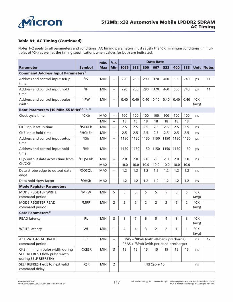
Table 81: AC Timing (Continued)
Notes 1–2 apply to all parameters and conditions. AC timing parameters must satisfy the tCK minimum conditions (in mul-tiples of tCK) as well as the timing specifications when values for both are indicated.
Parameter SymbolMin/Max
tCKMin
Data Rate
Unit Notes1066 933 800 667 533 400 333
Command Address Input Parameters3
Address and control input setuptime
tIS MIN – 220 250 290 370 460 600 740 ps 11
Address and control input holdtime
tIH MIN – 220 250 290 370 460 600 740 ps 11
Address and control input pulsewidth
tIPW MIN – 0.40 0.40 0.40 0.40 0.40 0.40 0.40 tCK(avg)
Boot Parameters (10 MHz–55 MHz)12, 13, 14
Clock cycle time tCKb MAX – 100 100 100 100 100 100 100 ns
MIN – 18 18 18 18 18 18 18
CKE input setup time tISCKEb MIN – 2.5 2.5 2.5 2.5 2.5 2.5 2.5 ns
CKE input hold time tIHCKEb MIN – 2.5 2.5 2.5 2.5 2.5 2.5 2.5 ns
Address and control input setuptime
tISb MIN – 1150 1150 1150 1150 1150 1150 1150 ps
Address and control input holdtime
tIHb MIN – 1150 1150 1150 1150 1150 1150 1150 ps
DQS output data access time fromCK/CK#
tDQSCKb MIN – 2.0 2.0 2.0 2.0 2.0 2.0 2.0 ns
MAX – 10.0 10.0 10.0 10.0 10.0 10.0 10.0
Data strobe edge to output dataedge
tDQSQb MAX – 1.2 1.2 1.2 1.2 1.2 1.2 1.2 ns
Data hold skew factor tQHSb MAX – 1.2 1.2 1.2 1.2 1.2 1.2 1.2 ns
Mode Register Parameters
MODE REGISTER WRITEcommand period
tMRW MIN 5 5 5 5 5 5 5 5 tCK(avg)
MODE REGISTER READcommand period
tMRR MIN 2 2 2 2 2 2 2 2 tCK(avg)
Core Parameters15
READ latency RL MIN 3 8 7 6 5 4 3 3 tCK(avg)
WRITE latency WL MIN 1 4 4 3 2 2 1 1 tCK(avg)
ACTIVATE-to-ACTIVATEcommand period
tRC MIN – tRAS + tRPab (with all-bank precharge),tRAS + tRPpb (with per-bank precharge)
ns 17
CKE minimum pulse width duringSELF REFRESH (low pulse widthduring SELF REFRESH)
tCKESR MIN 3 15 15 15 15 15 15 15 ns
SELF REFRESH exit to next validcommand delay
tXSR MIN 2 tRFCab + 10 ns
512Mb: x32 Automotive Mobile LPDDR2 SDRAMAC Timing
09005aef86573be0u97m_auto_lpddr2_ait_aat_aut.pdf - Rev. H 05/18 EN 117 Micron Technology, Inc. reserves the right to change products or specifications without notice.
© 2015 Micron Technology, Inc. All rights reserved.
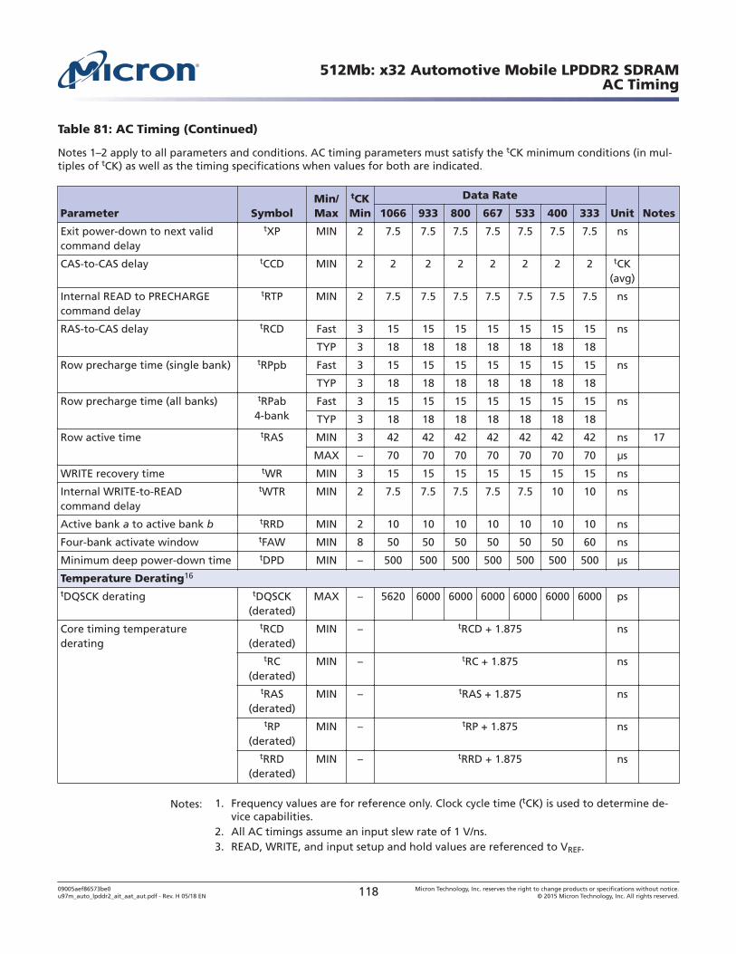
Table 81: AC Timing (Continued)
Notes 1–2 apply to all parameters and conditions. AC timing parameters must satisfy the tCK minimum conditions (in mul-tiples of tCK) as well as the timing specifications when values for both are indicated.
Parameter SymbolMin/Max
tCKMin
Data Rate
Unit Notes1066 933 800 667 533 400 333
Exit power-down to next validcommand delay
tXP MIN 2 7.5 7.5 7.5 7.5 7.5 7.5 7.5 ns
CAS-to-CAS delay tCCD MIN 2 2 2 2 2 2 2 2 tCK(avg)
Internal READ to PRECHARGEcommand delay
tRTP MIN 2 7.5 7.5 7.5 7.5 7.5 7.5 7.5 ns
RAS-to-CAS delay tRCD Fast 3 15 15 15 15 15 15 15 ns
TYP 3 18 18 18 18 18 18 18
Row precharge time (single bank) tRPpb Fast 3 15 15 15 15 15 15 15 ns
TYP 3 18 18 18 18 18 18 18
Row precharge time (all banks) tRPab4-bank
Fast 3 15 15 15 15 15 15 15 ns
TYP 3 18 18 18 18 18 18 18
Row active time tRAS MIN 3 42 42 42 42 42 42 42 ns 17
MAX – 70 70 70 70 70 70 70 μs
WRITE recovery time tWR MIN 3 15 15 15 15 15 15 15 ns
Internal WRITE-to-READcommand delay
tWTR MIN 2 7.5 7.5 7.5 7.5 7.5 10 10 ns
Active bank a to active bank b tRRD MIN 2 10 10 10 10 10 10 10 ns
Four-bank activate window tFAW MIN 8 50 50 50 50 50 50 60 ns
Minimum deep power-down time tDPD MIN – 500 500 500 500 500 500 500 μs
Temperature Derating16
tDQSCK derating tDQSCK(derated)
MAX – 5620 6000 6000 6000 6000 6000 6000 ps
Core timing temperaturederating
tRCD(derated)
MIN – tRCD + 1.875 ns
tRC(derated)
MIN – tRC + 1.875 ns
tRAS(derated)
MIN – tRAS + 1.875 ns
tRP(derated)
MIN – tRP + 1.875 ns
tRRD(derated)
MIN – tRRD + 1.875 ns
Notes: 1. Frequency values are for reference only. Clock cycle time (tCK) is used to determine de-vice capabilities.
2. All AC timings assume an input slew rate of 1 V/ns.3. READ, WRITE, and input setup and hold values are referenced to VREF.
512Mb: x32 Automotive Mobile LPDDR2 SDRAMAC Timing
09005aef86573be0u97m_auto_lpddr2_ait_aat_aut.pdf - Rev. H 05/18 EN 118 Micron Technology, Inc. reserves the right to change products or specifications without notice.
© 2015 Micron Technology, Inc. All rights reserved.
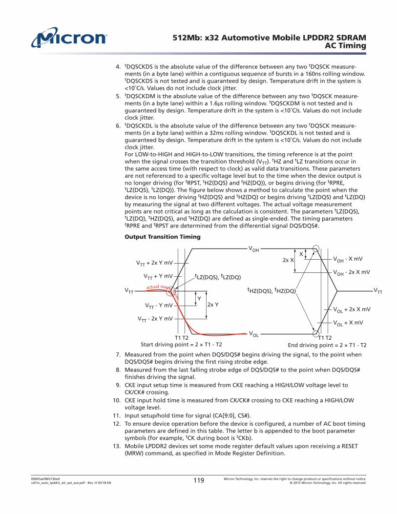
4. tDQSCKDS is the absolute value of the difference between any two tDQSCK measure-ments (in a byte lane) within a contiguous sequence of bursts in a 160ns rolling window.tDQSCKDS is not tested and is guaranteed by design. Temperature drift in the system is<10˚C/s. Values do not include clock jitter.
5. tDQSCKDM is the absolute value of the difference between any two tDQSCK measure-ments (in a byte lane) within a 1.6μs rolling window. tDQSCKDM is not tested and isguaranteed by design. Temperature drift in the system is <10˚C/s. Values do not includeclock jitter.
6. tDQSCKDL is the absolute value of the difference between any two tDQSCK measure-ments (in a byte lane) within a 32ms rolling window. tDQSCKDL is not tested and isguaranteed by design. Temperature drift in the system is <10˚C/s. Values do not includeclock jitter.For LOW-to-HIGH and HIGH-to-LOW transitions, the timing reference is at the pointwhen the signal crosses the transition threshold (VTT). tHZ and tLZ transitions occur inthe same access time (with respect to clock) as valid data transitions. These parametersare not referenced to a specific voltage level but to the time when the device output isno longer driving (for tRPST, tHZ(DQS) and tHZ(DQ)), or begins driving (for tRPRE,tLZ(DQS), tLZ(DQ)). The figure below shows a method to calculate the point when thedevice is no longer driving tHZ(DQS) and tHZ(DQ) or begins driving tLZ(DQS) and tLZ(DQ)by measuring the signal at two different voltages. The actual voltage measurementpoints are not critical as long as the calculation is consistent. The parameters tLZ(DQS),tLZ(DQ), tHZ(DQS), and tHZ(DQ) are defined as single-ended. The timing parameterstRPRE and tRPST are determined from the differential signal DQS/DQS#.
Output Transition Timing
VOL + 2x X mV
VOL + X mV
VOH - X mV
VOH - 2x X mV
2x XX
2x Y
VOH
VOL
Y
T1 T2
VTT - Y mV
VTT VTT
VTT - 2x Y mV
VTT + 2x Y mV
VTT + Y mV tLZ(DQS), tLZ(DQ)
tHZ(DQS), tHZ(DQ)
T1 T2Start driving point = 2 × T1 - T2 End driving point = 2 × T1 - T2
actual wave form
7. Measured from the point when DQS/DQS# begins driving the signal, to the point whenDQS/DQS# begins driving the first rising strobe edge.
8. Measured from the last falling strobe edge of DQS/DQS# to the point when DQS/DQS#finishes driving the signal.
9. CKE input setup time is measured from CKE reaching a HIGH/LOW voltage level toCK/CK# crossing.
10. CKE input hold time is measured from CK/CK# crossing to CKE reaching a HIGH/LOWvoltage level.
11. Input setup/hold time for signal (CA[9:0], CS#).12. To ensure device operation before the device is configured, a number of AC boot timing
parameters are defined in this table. The letter b is appended to the boot parametersymbols (for example, tCK during boot is tCKb).
13. Mobile LPDDR2 devices set some mode register default values upon receiving a RESET(MRW) command, as specified in Mode Register Definition.
512Mb: x32 Automotive Mobile LPDDR2 SDRAMAC Timing
09005aef86573be0u97m_auto_lpddr2_ait_aat_aut.pdf - Rev. H 05/18 EN 119 Micron Technology, Inc. reserves the right to change products or specifications without notice.
© 2015 Micron Technology, Inc. All rights reserved.
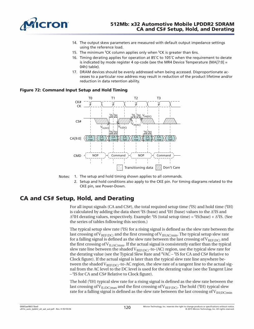
14. The output skew parameters are measured with default output impedance settingsusing the reference load.
15. The minimum tCK column applies only when tCK is greater than 6ns.16. Timing derating applies for operation at 85˚C to 105˚C when the requirement to derate
is indicated by mode register 4 op-code (see the MR4 Device Temperature (MA[7:0] =04h) table).
17. DRAM devices should be evenly addressed when being accessed. Disproportionate ac-cesses to a particular row address may result in reduction of the product lifetime and/orreduction in data retention ability.
Figure 72: Command Input Setup and Hold Timing
tIS tIH
CommandNOP Command
T0 T1 T2 T3CK#
CK
CS#
CAriseCA[9:0]
CMD
Don’t CareTransitioning data
CAfall
CArise
CAfall
CArise
CAfall
CArise
CAfall
NOP
tIS tIH
tIS tIH tIS tIH
VIL(AC)
VIH(DC)
VIH(AC)VIL(DC)
Notes: 1. The setup and hold timing shown applies to all commands.2. Setup and hold conditions also apply to the CKE pin. For timing diagrams related to the
CKE pin, see Power-Down.
CA and CS# Setup, Hold, and DeratingFor all input signals (CA and CS#), the total required setup time (tIS) and hold time (tIH)is calculated by adding the data sheet tIS (base) and tIH (base) values to the tIS and
tIH derating values, respectively. Example: tIS (total setup time) = tIS(base) + tIS. (Seethe series of tables following this section.)
The typical setup slew rate (tIS) for a rising signal is defined as the slew rate between thelast crossing of VREF(DC) and the first crossing of VIH(AC)min. The typical setup slew ratefor a falling signal is defined as the slew rate between the last crossing of VREF(DC) andthe first crossing of VIL(AC)max. If the actual signal is consistently earlier than the typicalslew rate line between the shaded VREF(DC)-to-(AC) region, use the typical slew rate forthe derating value (see the Typical Slew Rate and tVAC – tIS for CA and CS# Relative toClock figure). If the actual signal is later than the typical slew rate line anywhere be-tween the shaded VREF(DC)-to-AC region, the slew rate of a tangent line to the actual sig-nal from the AC level to the DC level is used for the derating value (see the Tangent Line– tIS for CA and CS# Relative to Clock figure).
The hold (tIH) typical slew rate for a rising signal is defined as the slew rate between thelast crossing of VIL(DC)max and the first crossing of VREF(DC). The hold (tIH) typical slewrate for a falling signal is defined as the slew rate between the last crossing of VIH(DC)min
512Mb: x32 Automotive Mobile LPDDR2 SDRAMCA and CS# Setup, Hold, and Derating
09005aef86573be0u97m_auto_lpddr2_ait_aat_aut.pdf - Rev. H 05/18 EN 120 Micron Technology, Inc. reserves the right to change products or specifications without notice.
© 2015 Micron Technology, Inc. All rights reserved.
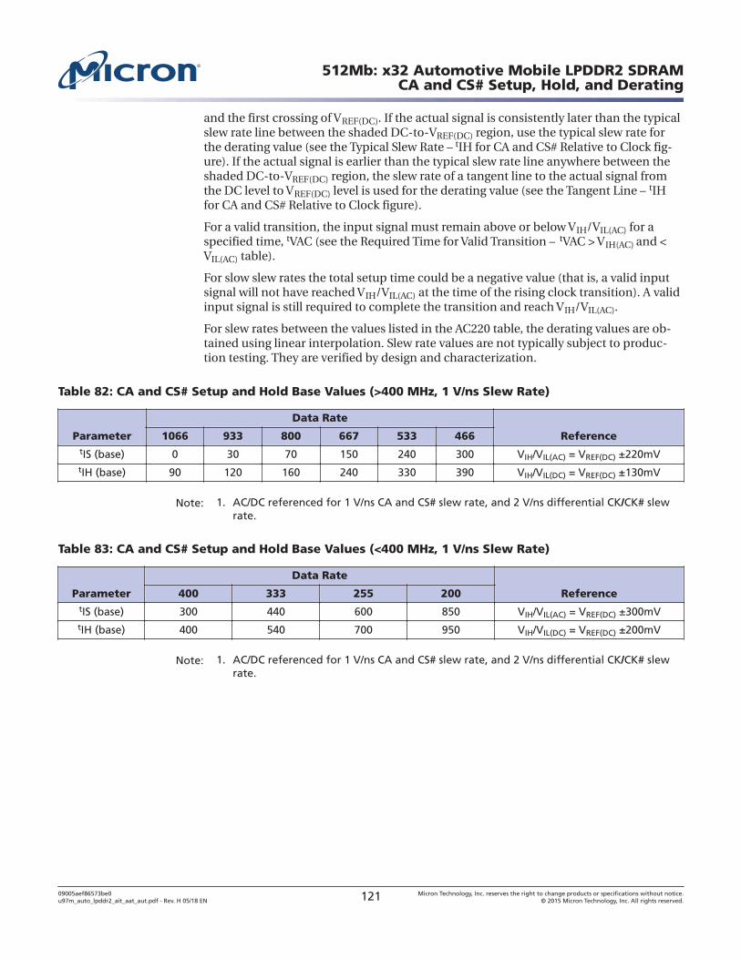
and the first crossing of VREF(DC). If the actual signal is consistently later than the typicalslew rate line between the shaded DC-to-VREF(DC) region, use the typical slew rate forthe derating value (see the Typical Slew Rate – tIH for CA and CS# Relative to Clock fig-ure). If the actual signal is earlier than the typical slew rate line anywhere between theshaded DC-to-VREF(DC) region, the slew rate of a tangent line to the actual signal fromthe DC level to VREF(DC) level is used for the derating value (see the Tangent Line – tIHfor CA and CS# Relative to Clock figure).
For a valid transition, the input signal must remain above or below VIH/VIL(AC) for aspecified time, tVAC (see the Required Time for Valid Transition – tVAC > VIH(AC) and <VIL(AC) table).
For slow slew rates the total setup time could be a negative value (that is, a valid inputsignal will not have reached VIH/VIL(AC) at the time of the rising clock transition). A validinput signal is still required to complete the transition and reach VIH/VIL(AC).
For slew rates between the values listed in the AC220 table, the derating values are ob-tained using linear interpolation. Slew rate values are not typically subject to produc-tion testing. They are verified by design and characterization.
Table 82: CA and CS# Setup and Hold Base Values (>400 MHz, 1 V/ns Slew Rate)
Parameter
Data Rate
Reference1066 933 800 667 533 466tIS (base) 0 30 70 150 240 300 VIH/VIL(AC) = VREF(DC) ±220mVtIH (base) 90 120 160 240 330 390 VIH/VIL(DC) = VREF(DC) ±130mV
Note: 1. AC/DC referenced for 1 V/ns CA and CS# slew rate, and 2 V/ns differential CK/CK# slewrate.
Table 83: CA and CS# Setup and Hold Base Values (<400 MHz, 1 V/ns Slew Rate)
Parameter
Data Rate
Reference400 333 255 200tIS (base) 300 440 600 850 VIH/VIL(AC) = VREF(DC) ±300mVtIH (base) 400 540 700 950 VIH/VIL(DC) = VREF(DC) ±200mV
Note: 1. AC/DC referenced for 1 V/ns CA and CS# slew rate, and 2 V/ns differential CK/CK# slewrate.
512Mb: x32 Automotive Mobile LPDDR2 SDRAMCA and CS# Setup, Hold, and Derating
09005aef86573be0u97m_auto_lpddr2_ait_aat_aut.pdf - Rev. H 05/18 EN 121 Micron Technology, Inc. reserves the right to change products or specifications without notice.
© 2015 Micron Technology, Inc. All rights reserved.
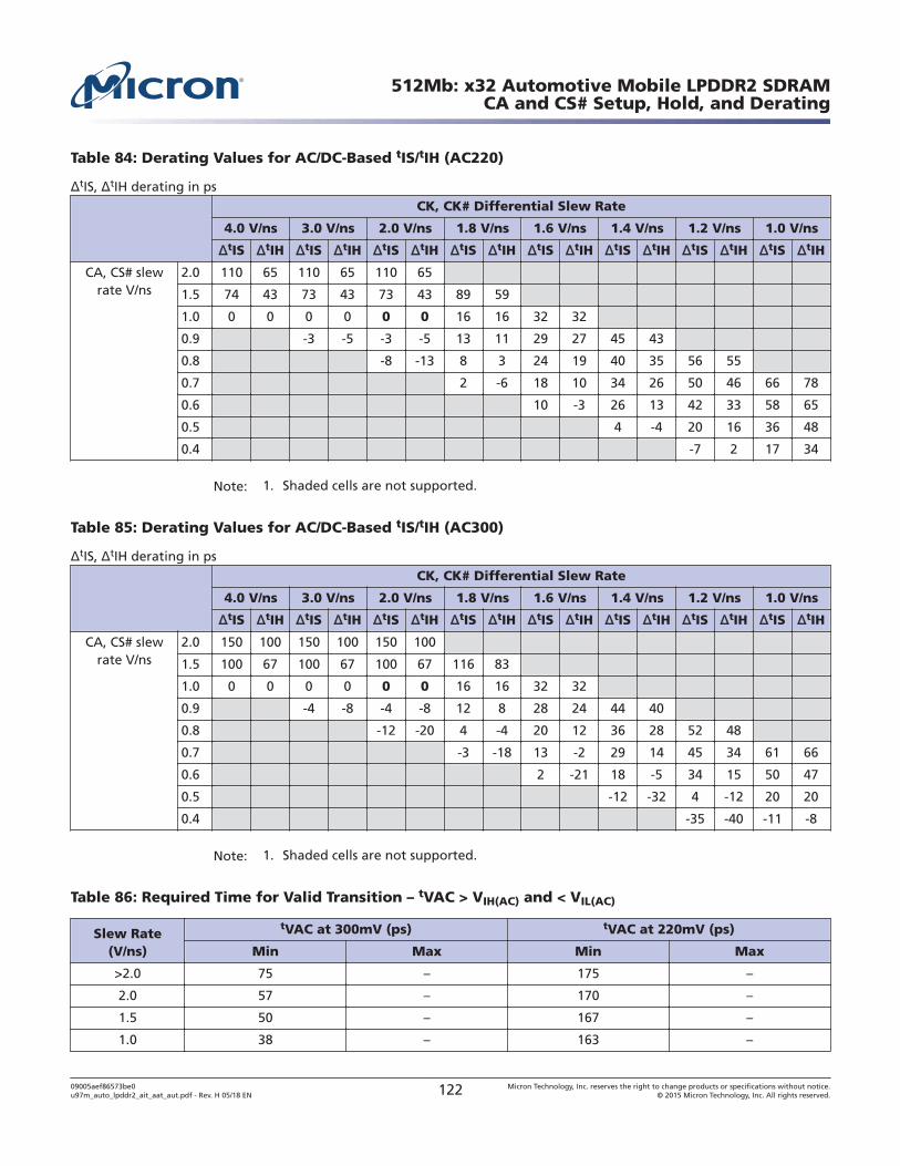
Table 84: Derating Values for AC/DC-Based tIS/tIH (AC220)
ΔtIS, ΔtIH derating in ps
CK, CK# Differential Slew Rate
4.0 V/ns 3.0 V/ns 2.0 V/ns 1.8 V/ns 1.6 V/ns 1.4 V/ns 1.2 V/ns 1.0 V/ns
ΔΔtIS ΔtIH ΔtIS ΔtIH ΔtIS ΔtIH ΔtIS ΔtIH ΔtIS ΔtIH ΔtIS ΔtIH ΔtIS ΔtIH ΔtIS ΔtIH
CA, CS# slewrate V/ns
2.0 110 65 110 65 110 65
1.5 74 43 73 43 73 43 89 59
1.0 0 0 0 0 0 0 16 16 32 32
0.9 -3 -5 -3 -5 13 11 29 27 45 43
0.8 -8 -13 8 3 24 19 40 35 56 55
0.7 2 -6 18 10 34 26 50 46 66 78
0.6 10 -3 26 13 42 33 58 65
0.5 4 -4 20 16 36 48
0.4 -7 2 17 34
Note: 1. Shaded cells are not supported.
Table 85: Derating Values for AC/DC-Based tIS/tIH (AC300)
ΔtIS, ΔtIH derating in ps
CK, CK# Differential Slew Rate
4.0 V/ns 3.0 V/ns 2.0 V/ns 1.8 V/ns 1.6 V/ns 1.4 V/ns 1.2 V/ns 1.0 V/ns
ΔtIS ΔtIH ΔtIS ΔtIH ΔtIS ΔtIH ΔtIS ΔtIH ΔtIS ΔtIH ΔtIS ΔtIH ΔtIS ΔtIH ΔtIS ΔtIH
CA, CS# slewrate V/ns
2.0 150 100 150 100 150 100
1.5 100 67 100 67 100 67 116 83
1.0 0 0 0 0 0 0 16 16 32 32
0.9 -4 -8 -4 -8 12 8 28 24 44 40
0.8 -12 -20 4 -4 20 12 36 28 52 48
0.7 -3 -18 13 -2 29 14 45 34 61 66
0.6 2 -21 18 -5 34 15 50 47
0.5 -12 -32 4 -12 20 20
0.4 -35 -40 -11 -8
Note: 1. Shaded cells are not supported.
Table 86: Required Time for Valid Transition – tVAC > VIH(AC) and < VIL(AC)
Slew Rate(V/ns)
tVAC at 300mV (ps) tVAC at 220mV (ps)
Min Max Min Max
>2.0 75 – 175 –
2.0 57 – 170 –
1.5 50 – 167 –
1.0 38 – 163 –
512Mb: x32 Automotive Mobile LPDDR2 SDRAMCA and CS# Setup, Hold, and Derating
09005aef86573be0u97m_auto_lpddr2_ait_aat_aut.pdf - Rev. H 05/18 EN 122 Micron Technology, Inc. reserves the right to change products or specifications without notice.
© 2015 Micron Technology, Inc. All rights reserved.
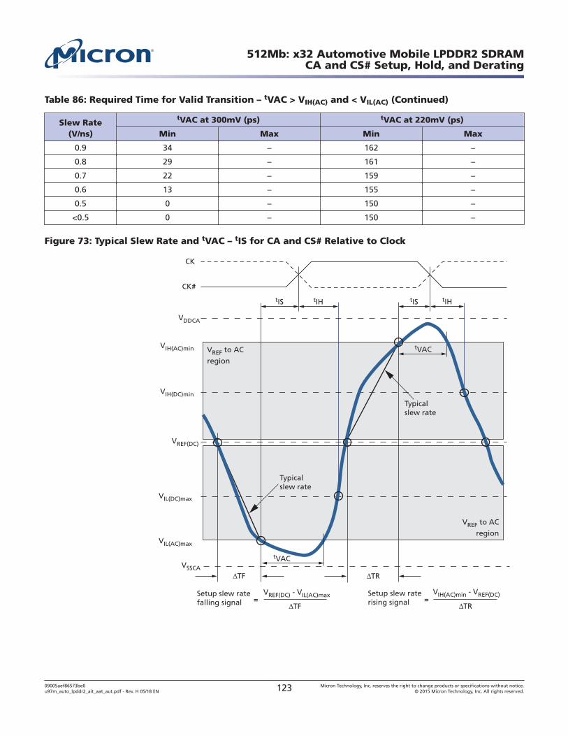
Table 86: Required Time for Valid Transition – tVAC > VIH(AC) and < VIL(AC) (Continued)
Slew Rate(V/ns)
tVAC at 300mV (ps) tVAC at 220mV (ps)
Min Max Min Max
0.9 34 – 162 –
0.8 29 – 161 –
0.7 22 – 159 –
0.6 13 – 155 –
0.5 0 – 150 –
<0.5 0 – 150 –
Figure 73: Typical Slew Rate and tVAC – tIS for CA and CS# Relative to Clock
VSSCA
CK#
CK
tVAC
Setup slew raterising signal
Setup slew rate falling signal
TF TR
TF=
VIH(AC)min - VREF(DC)
TR=
VDDCA
Typicalslew rate
VREF to AC
region
VREF to AC
region
VREF(DC) - VIL(AC)max
VIH(DC)min
VREF(DC)
VIL(AC)max
VIL(DC)max
VIH(AC)min
Typicalslew rate
tIHtIS tIStIH
tVAC
512Mb: x32 Automotive Mobile LPDDR2 SDRAMCA and CS# Setup, Hold, and Derating
09005aef86573be0u97m_auto_lpddr2_ait_aat_aut.pdf - Rev. H 05/18 EN 123 Micron Technology, Inc. reserves the right to change products or specifications without notice.
© 2015 Micron Technology, Inc. All rights reserved.
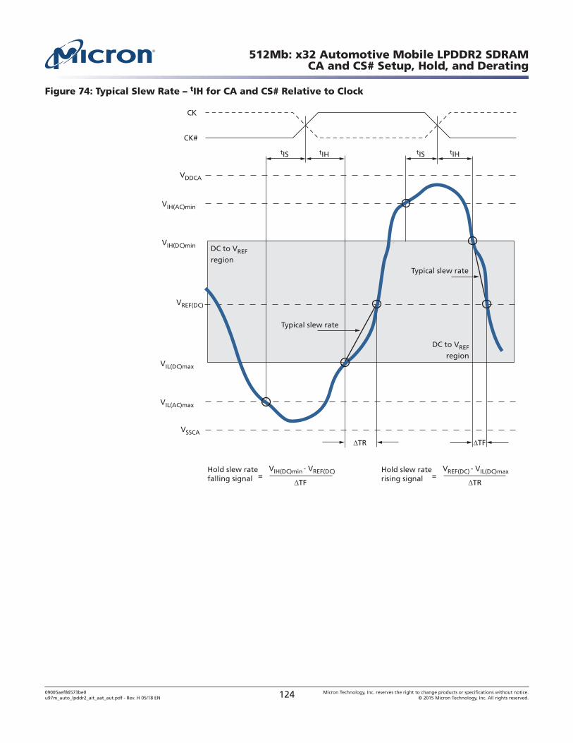
Figure 74: Typical Slew Rate – tIH for CA and CS# Relative to Clock
TR TF
Typical slew rate
DC to VREFregion
VSSCA
CK#
CK
VDDCA
VIH(DC)min
VREF(DC)
VIL(AC)max
VIL(DC)max
VIH(AC)min
DC to VREFregion
Typical slew rate
Hold slew rate rising signal
VREF(DC) - VIL(DC)max
TR=
Hold slew rate falling signal
VIH(DC)min - VREF(DC)
TF=
tIHtIS tIStIH
512Mb: x32 Automotive Mobile LPDDR2 SDRAMCA and CS# Setup, Hold, and Derating
09005aef86573be0u97m_auto_lpddr2_ait_aat_aut.pdf - Rev. H 05/18 EN 124 Micron Technology, Inc. reserves the right to change products or specifications without notice.
© 2015 Micron Technology, Inc. All rights reserved.
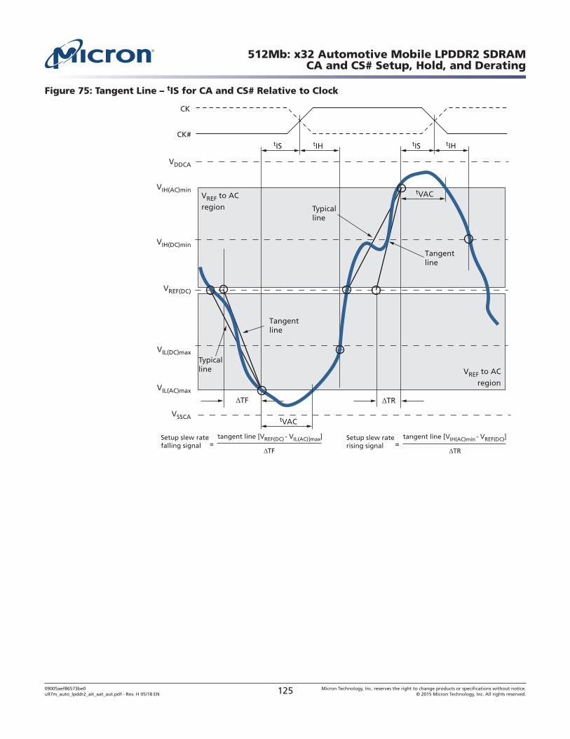
Figure 75: Tangent Line – tIS for CA and CS# Relative to Clock
Setup slew rate rising signal
TF TR
tangent line [VIH(AC)min - VREF(DC)]
TR=
Setup slew rate falling signal
tangent line [VREF(DC) - VIL(AC)]max]
TF=
Tangentline
Tangent line
VREF to AC
region Typicalline
Typicalline
VSSCA
CK#
CK
VDDCA
VIH(AC)min
VIH(DC)min
VREF(DC)
VIL(DC)max
VIL(AC)max
VREF to AC
region
tVAC
tIHtIS tIStIH
tVAC
512Mb: x32 Automotive Mobile LPDDR2 SDRAMCA and CS# Setup, Hold, and Derating
09005aef86573be0u97m_auto_lpddr2_ait_aat_aut.pdf - Rev. H 05/18 EN 125 Micron Technology, Inc. reserves the right to change products or specifications without notice.
© 2015 Micron Technology, Inc. All rights reserved.
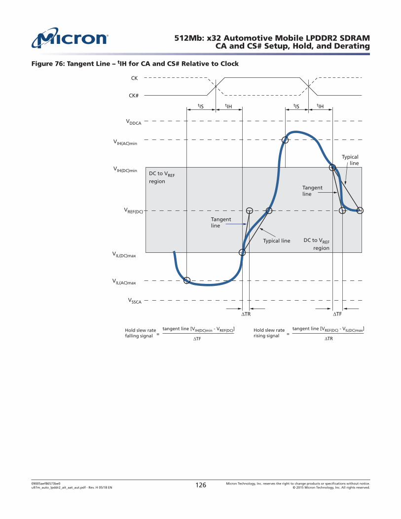
Figure 76: Tangent Line – tIH for CA and CS# Relative to Clock
Tangent line
DC to VREFregion
tIHtIS tIS
VSSCA
VDDCA
VIH(DC)min
VREF(DC)
VIL(AC)max
VIL(DC)max
VIH(AC)min
DC to VREF
regionTangent line
tIH
CK
CK#
Hold slew rate falling signal
TFTR
tangent line [VIH(DC)min - VREF(DC)]
TF=
Typical line
Hold slew rate rising signal
tangent line [VREF(DC) - VIL(DC)max]
TR=
Typicalline
512Mb: x32 Automotive Mobile LPDDR2 SDRAMCA and CS# Setup, Hold, and Derating
09005aef86573be0u97m_auto_lpddr2_ait_aat_aut.pdf - Rev. H 05/18 EN 126 Micron Technology, Inc. reserves the right to change products or specifications without notice.
© 2015 Micron Technology, Inc. All rights reserved.
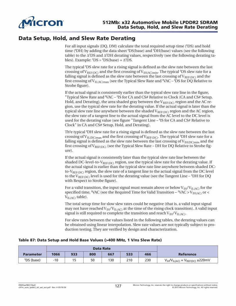
Data Setup, Hold, and Slew Rate DeratingFor all input signals (DQ, DM) calculate the total required setup time (tDS) and holdtime (tDH) by adding the data sheet tDS(base) and tDH(base) values (see the followingtable) to the tDS and tDH derating values, respectively (see the following derating ta-bles). Example: tDS = tDS(base) + tDS.
The typical tDS slew rate for a rising signal is defined as the slew rate between the lastcrossing of VREF(DC) and the first crossing of VIH(AC)min. The typical tDS slew rate for afalling signal is defined as the slew rate between the last crossing of VREF(DC) and thefirst crossing of VIL(AC)max (see the Typical Slew Rate and tVAC – tDS for DQ Relative toStrobe figure).
If the actual signal is consistently earlier than the typical slew rate line in the figure,"Typical Slew Rate and tVAC – tIS for CA and CS# Relative to Clock (CA and CS# Setup,Hold, and Derating), the area shaded gray between the VREF(DC) region and the AC re-gion, use the typical slew rate for the derating value. If the actual signal is later than thetypical slew rate line anywhere between the shaded VREF(DC) region and the AC region,the slew rate of a tangent line to the actual signal from the AC level to the DC level isused for the derating value (see figure "Tangent Line – tIS for CA and CS# Relative toClock" in CA and CS# Setup, Hold, and Derating).
Thte typical tDH slew rate for a rising signal is defined as the slew rate between the lastcrossing of VIL(DC)max and the first crossing of VREF(DC). The typical tDH slew rate for afalling signal is defined as the slew rate between the last crossing of VIH(DC)min and thefirst crossing of VREF(DC) (see the Typical Slew Rate – DH for DQ Relative to Strobe fig-ure).
If the actual signal is consistently later than the typical slew rate line between theshaded DC-level-to-VREF(DC) region, use the typical slew rate for the derating value. Ifthe actual signal is earlier than the typical slew rate line anywhere between shaded DC-to-VREF(DC) region, the slew rate of a tangent line to the actual signal from the DC levelto the VREF(DC) level is used for the derating value (see the Tangent Line – tDH for DQwith Respect to Strobe figure).
For a valid transition, the input signal must remain above or below VIH/VIL(AC) for thespecified time, tVAC (see the Required Time for Valid Transition – tVAC > VIH(AC) or <VIL(AC) table).
The total setup time for slow slew rates could be negative (that is, a valid input signalmay not have reached VIH/VIL(AC) at the time of the rising clock transition). A valid inputsignal is still required to complete the transition and reach VIH/VIL(AC).
For slew rates between the values listed in the following tables, the derating values canbe obtained using linear interpolation. Slew rate values are not typically subject to pro-duction testing. They are verified by design and characterization.
Table 87: Data Setup and Hold Base Values (>400 MHz, 1 V/ns Slew Rate)
Parameter
Data Rate
Reference1066 933 800 667 533 466tDS (base) -10 15 50 130 210 230 VIH/VIL(AC) = VREF(DC) ±220mV
512Mb: x32 Automotive Mobile LPDDR2 SDRAMData Setup, Hold, and Slew Rate Derating
09005aef86573be0u97m_auto_lpddr2_ait_aat_aut.pdf - Rev. H 05/18 EN 127 Micron Technology, Inc. reserves the right to change products or specifications without notice.
© 2015 Micron Technology, Inc. All rights reserved.
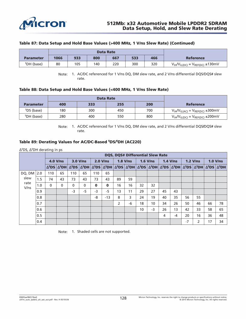
Table 87: Data Setup and Hold Base Values (>400 MHz, 1 V/ns Slew Rate) (Continued)
Parameter
Data Rate
Reference1066 933 800 667 533 466tDH (base) 80 105 140 220 300 320 VIH/VIL(DC) = VREF(DC) ±130mV
Note: 1. AC/DC referenced for 1 V/ns DQ, DM slew rate, and 2 V/ns differential DQS/DQS# slewrate.
Table 88: Data Setup and Hold Base Values (<400 MHz, 1 V/ns Slew Rate)
Parameter
Data Rate
Reference400 333 255 200tDS (base) 180 300 450 700 VIH/VIL(AC) = VREF(DC) ±300mVtDH (base) 280 400 550 800 VIH/VIL(DC) = VREF(DC) ±200mV
Note: 1. AC/DC referenced for 1 V/ns DQ, DM slew rate, and 2 V/ns differential DQS/DQS# slewrate.
Table 89: Derating Values for AC/DC-Based tDS/tDH (AC220)
ΔtDS, ΔtDH derating in ps
DQS, DQS# Differential Slew Rate
4.0 V/ns 3.0 V/ns 2.0 V/ns 1.8 V/ns 1.6 V/ns 1.4 V/ns 1.2 V/ns 1.0 V/ns
ΔΔtDS ΔtDH ΔtDS ΔtDH ΔtDS ΔtDH ΔtDS ΔtDH ΔtDS ΔtDH ΔtDS ΔtDH ΔtDS ΔtDH ΔtDS ΔtDH
DQ, DMslewrateV/ns
2.0 110 65 110 65 110 65
1.5 74 43 73 43 73 43 89 59
1.0 0 0 0 0 0 0 16 16 32 32
0.9 -3 -5 -3 -5 13 11 29 27 45 43
0.8 -8 -13 8 3 24 19 40 35 56 55
0.7 2 -6 18 10 34 26 50 46 66 78
0.6 10 -3 26 13 42 33 58 65
0.5 4 -4 20 16 36 48
0.4 -7 2 17 34
Note: 1. Shaded cells are not supported.
512Mb: x32 Automotive Mobile LPDDR2 SDRAMData Setup, Hold, and Slew Rate Derating
09005aef86573be0u97m_auto_lpddr2_ait_aat_aut.pdf - Rev. H 05/18 EN 128 Micron Technology, Inc. reserves the right to change products or specifications without notice.
© 2015 Micron Technology, Inc. All rights reserved.
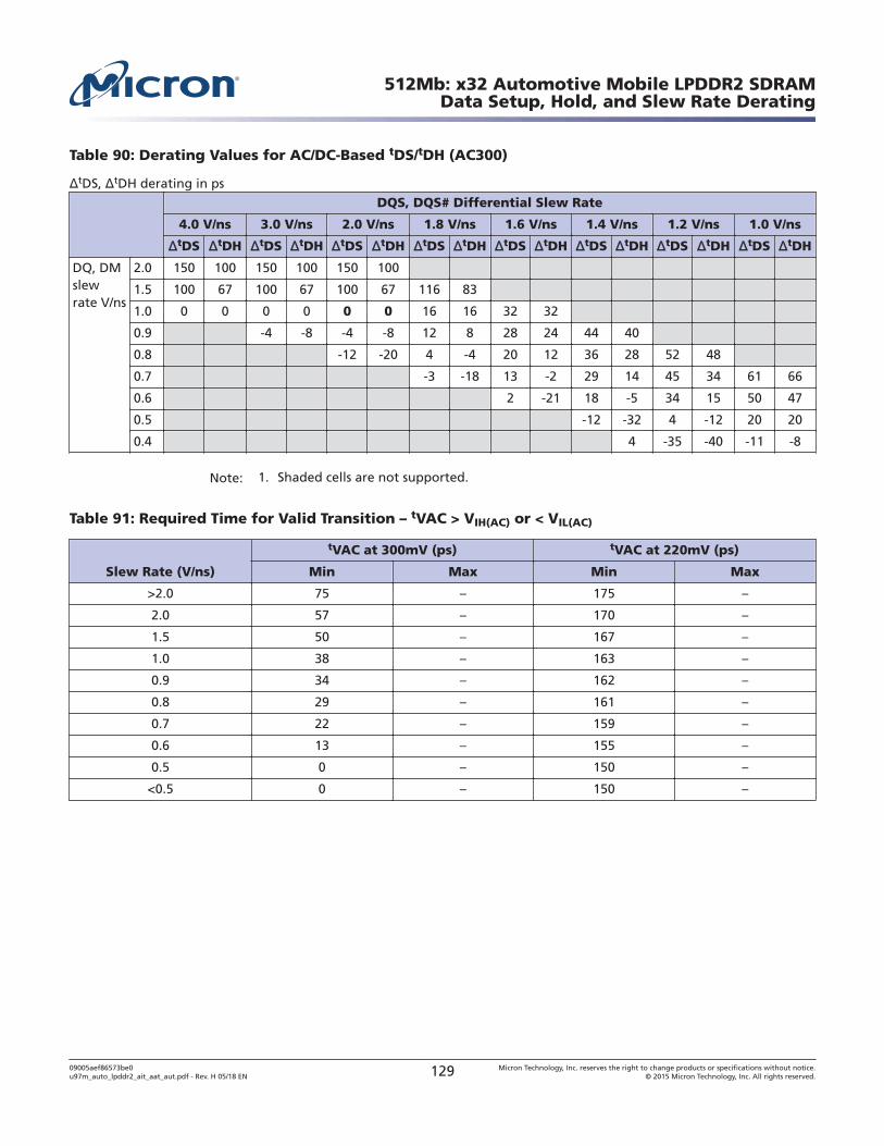
Table 90: Derating Values for AC/DC-Based tDS/tDH (AC300)
ΔtDS, ΔtDH derating in ps
DQS, DQS# Differential Slew Rate
4.0 V/ns 3.0 V/ns 2.0 V/ns 1.8 V/ns 1.6 V/ns 1.4 V/ns 1.2 V/ns 1.0 V/ns
ΔΔtDS ΔtDH ΔtDS ΔtDH ΔtDS ΔtDH ΔtDS ΔtDH ΔtDS ΔtDH ΔtDS ΔtDH ΔtDS ΔtDH ΔtDS ΔtDH
DQ, DMslewrate V/ns
2.0 150 100 150 100 150 100
1.5 100 67 100 67 100 67 116 83
1.0 0 0 0 0 0 0 16 16 32 32
0.9 -4 -8 -4 -8 12 8 28 24 44 40
0.8 -12 -20 4 -4 20 12 36 28 52 48
0.7 -3 -18 13 -2 29 14 45 34 61 66
0.6 2 -21 18 -5 34 15 50 47
0.5 -12 -32 4 -12 20 20
0.4 4 -35 -40 -11 -8
Note: 1. Shaded cells are not supported.
Table 91: Required Time for Valid Transition – tVAC > VIH(AC) or < VIL(AC)
Slew Rate (V/ns)
tVAC at 300mV (ps) tVAC at 220mV (ps)
Min Max Min Max
>2.0 75 – 175 –
2.0 57 – 170 –
1.5 50 – 167 –
1.0 38 – 163 –
0.9 34 – 162 –
0.8 29 – 161 –
0.7 22 – 159 –
0.6 13 – 155 –
0.5 0 – 150 –
<0.5 0 – 150 –
512Mb: x32 Automotive Mobile LPDDR2 SDRAMData Setup, Hold, and Slew Rate Derating
09005aef86573be0u97m_auto_lpddr2_ait_aat_aut.pdf - Rev. H 05/18 EN 129 Micron Technology, Inc. reserves the right to change products or specifications without notice.
© 2015 Micron Technology, Inc. All rights reserved.
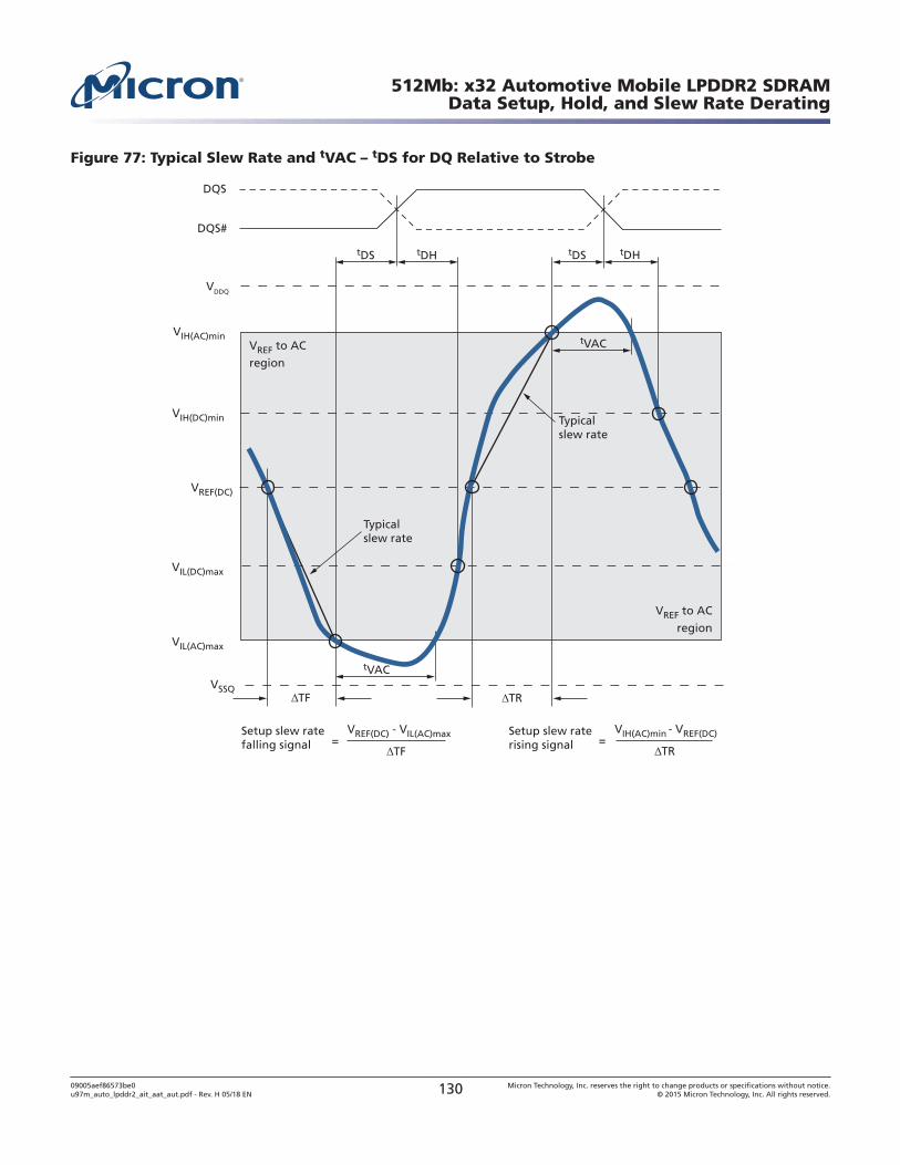
Figure 77: Typical Slew Rate and tVAC – tDS for DQ Relative to Strobe
VREF to AC
region
VREF to AC
region
Setup slew raterising signal
Setup slew ratefalling signal
TF TR
VREF(DC) - VIL(AC)max
TF=
VIH(AC)min - VREF(DC)
TR=
Typical slew rate
VSSQ
DQS#
DQS
VDDQ
VIH(DC)min
VREF(DC)
VIL(AC)max
VIL(DC)max
VIH(AC)min
Typical slew rate
tVAC
tVAC
tDHtDS tDStDH
512Mb: x32 Automotive Mobile LPDDR2 SDRAMData Setup, Hold, and Slew Rate Derating
09005aef86573be0u97m_auto_lpddr2_ait_aat_aut.pdf - Rev. H 05/18 EN 130 Micron Technology, Inc. reserves the right to change products or specifications without notice.
© 2015 Micron Technology, Inc. All rights reserved.
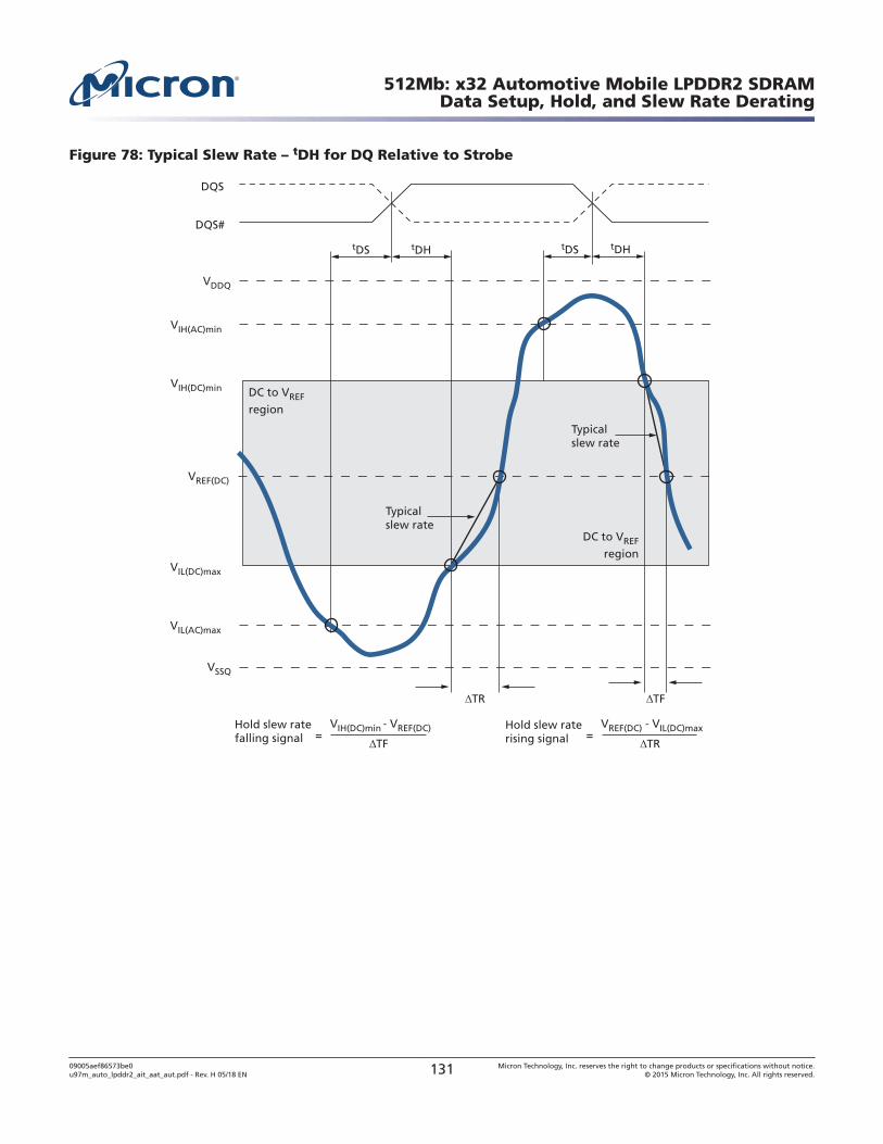
Figure 78: Typical Slew Rate – tDH for DQ Relative to Strobe
Hold slew ratefalling signal
Hold slew raterising signal
VREF(DC) - VIL(DC)max
TR=
VIH(DC)min - VREF(DC)
TF=
TR TF
Typical slew rate
DC to VREFregion
VSSQ
DQS#
DQS
VDDQ
VIH(DC)min
VREF(DC)
VIL(AC)max
VIL(DC)max
VIH(AC)min
DC to VREF region
Typical slew rate
tDHtDS tDStDH
512Mb: x32 Automotive Mobile LPDDR2 SDRAMData Setup, Hold, and Slew Rate Derating
09005aef86573be0u97m_auto_lpddr2_ait_aat_aut.pdf - Rev. H 05/18 EN 131 Micron Technology, Inc. reserves the right to change products or specifications without notice.
© 2015 Micron Technology, Inc. All rights reserved.
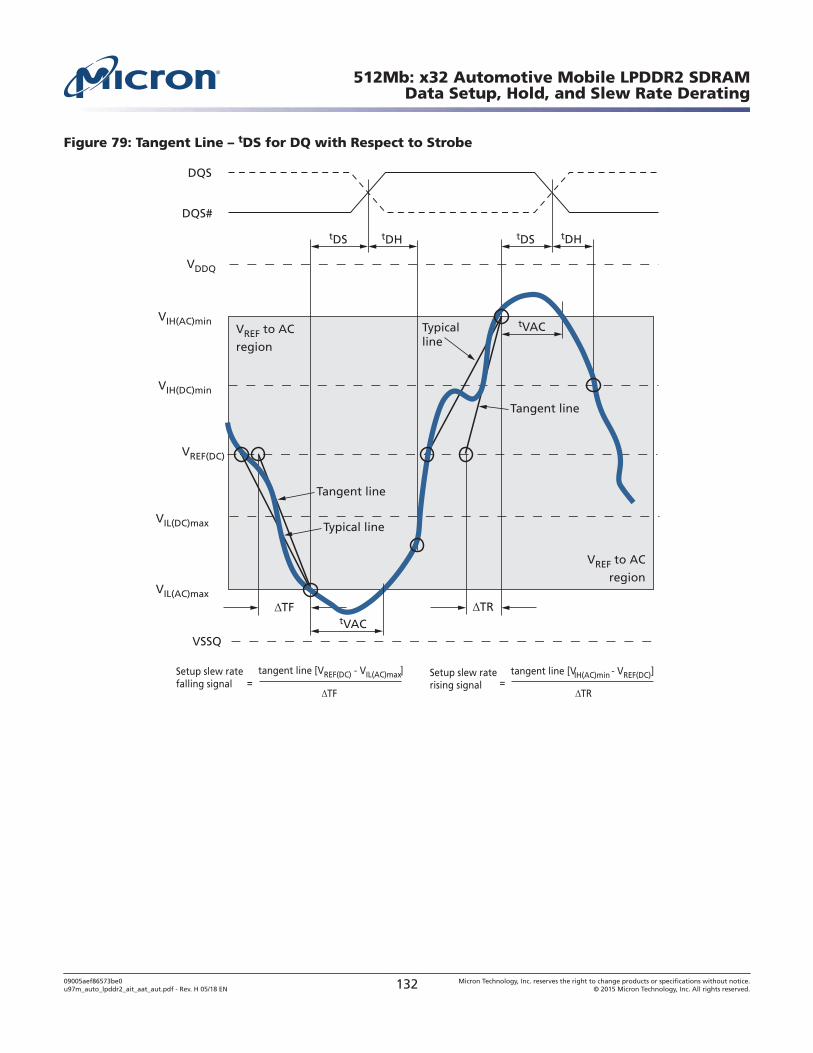
Figure 79: Tangent Line – tDS for DQ with Respect to Strobe
TF TR
Setup slew raterising signal
Setup slew ratefalling signal
tangent line [VREF(DC) - VIL(AC)max]
TF=
tangent line [VIH(AC)min - VREF(DC)]
TR=
VSSQ
DQS#
DQS
VDDQ
VIH(DC)min
VREF(DC)
VIL(AC)max
VIL(DC)max
VIH(AC)min
Typical line
Tangent line
Typicalline
Tangent line
VREF to AC
region
VREF to AC
region
tVAC
tDHtDS tDStDH
tVAC
512Mb: x32 Automotive Mobile LPDDR2 SDRAMData Setup, Hold, and Slew Rate Derating
09005aef86573be0u97m_auto_lpddr2_ait_aat_aut.pdf - Rev. H 05/18 EN 132 Micron Technology, Inc. reserves the right to change products or specifications without notice.
© 2015 Micron Technology, Inc. All rights reserved.
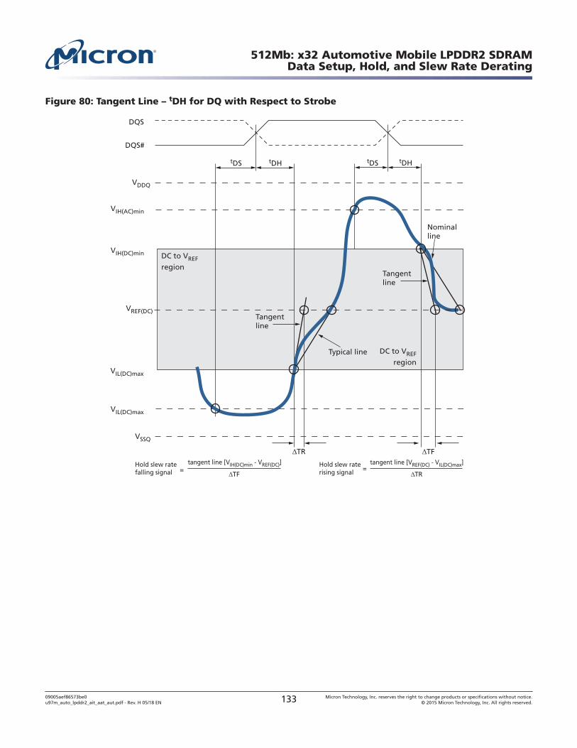
Figure 80: Tangent Line – tDH for DQ with Respect to Strobe
Tangent line
DC to VREFregion
VSSQ
VDDQ
VIH(DC)min
VREF(DC)
VIL(DC)max
VIL(DC)max
VIH(AC)min
DC to VREFregion
Tangent line
DQS
DQS#
Hold slew rate falling signal
TFTRtangent line [VIH(DC)min - VREF(DC)]
TF=
Typical line
Hold slew raterising signal
tangent line [VREF(DC) - VIL(DC)max]
TR=
Nominal line
tDHtDS tDStDH
512Mb: x32 Automotive Mobile LPDDR2 SDRAMData Setup, Hold, and Slew Rate Derating
09005aef86573be0u97m_auto_lpddr2_ait_aat_aut.pdf - Rev. H 05/18 EN 133 Micron Technology, Inc. reserves the right to change products or specifications without notice.
© 2015 Micron Technology, Inc. All rights reserved.
Revision History
Rev. H – 05/18
• Added Important Notes and Warnings section for further clarification aligning to in-dustry standards
Rev. G – 07/17
• Correction of tMRW from 3tCK to 5tCK.
Rev. F – 01/17
• Updated further tRAS, tRC footnote clarification.
Rev. E – 04/16
• Updated MR6 Op-Code Bit Definitions table, MR7 Op-Code Bit Definitions table, andMR16 Op-Code Bit Definitions table in Mode Register Definition section
• Deleted MR17 PASR Segment Mask Definitions table and MR17 PASR Row AddressRanges in Masked Segments table in Mode Register Definition section
• Updated Bank Selection for PRECHARGE by Address Bits table (Removed columnBA2) in PRECHARGE Command section
• Deleted Partial-Array Self Refresh – Segment Masking section• Deleted Bank and Segment Masking Example table in SELF REFRESH Operation sec-
tion• Updated Command Truth Table in Truth Tables section
Rev. D – 01/16
• Typo correction in 512Mb LPDDR2 Part Numbering figure in Feature
Rev. C – 12/15
• Updated IDD6 Partial-Array Self Refresh Current table in IDD Specifications section• Added note about VDDCA pin treatment for 134-Ball VFBGA and 168-Ball WFBGA in
Ball Assignments and Descriptions section
Rev. B – 10/15
• Added Iddx values, and refresh requirements for AUT option.
Rev. A – 07/15
• Initial release• Used LPDDR2 U87M 512mb_mobile_lpddr2_u87n_ait_aat.pdf as basis; Rev B, pub-
lished 2/15 (PDF: 09005aef85fcf570)
512Mb: x32 Automotive Mobile LPDDR2 SDRAMRevision History
09005aef86573be0u97m_auto_lpddr2_ait_aat_aut.pdf - Rev. H 05/18 EN 134 Micron Technology, Inc. reserves the right to change products or specifications without notice.
© 2015 Micron Technology, Inc. All rights reserved.
8000 S. Federal Way, P.O. Box 6, Boise, ID 83707-0006, Tel: 208-368-4000www.micron.com/products/support Sales inquiries: 800-932-4992
Micron and the Micron logo are trademarks of Micron Technology, Inc.All other trademarks are the property of their respective owners.
This data sheet contains minimum and maximum limits specified over the power supply and temperature range set forth herein.Although considered final, these specifications are subject to change, as further product development and data characterization some-
times occur.
512Mb: x32 Automotive Mobile LPDDR2 SDRAMRevision History
09005aef86573be0u97m_auto_lpddr2_ait_aat_aut.pdf - Rev. H 05/18 EN 135 Micron Technology, Inc. reserves the right to change products or specifications without notice.
© 2015 Micron Technology, Inc. All rights reserved.