Embed Size (px)
Citation preview
Preliminary Specifications
512 Kbit / 1 Mbit / 2 Mbit / 4 Mbit (x8) Small-Sector FlashSST29SF512 / SST29SF010 / SST29SF020 / SST29SF040SST29VF512 / SST29VF010 / SST29VF020 / SST29VF040
FEATURES:
• Organized as 64K x8 / 128K x8 / 256K x8 / 512K x8• Single Voltage Read and Write Operations
– 4.5-5.5V-only for SST29SF512/010/020/040– 2.7-3.6V for SST29VF512/010/020/040
• Superior Reliability– Endurance: 100,000 Cycles (typical)– Greater than 100 years Data Retention
• Low Power Consumption:– Active Current: 10 mA (typical)– Standby Current:
30 µA (typical) for SST29SF512/010/020/0401 µA (typical) for SST29VF512/010/020/040
• Sector-Erase Capability– Uniform 128 Byte sectors
• Fast Read Access Time:– 55 ns– 70 ns
• Latched Address and Data
• Fast Erase and Byte-Program:– Sector-Erase Time: 18 ms (typical)– Chip-Erase Time: 70 ms (typical)– Byte-Program Time: 14 µs (typical)– Chip Rewrite Time:
1 second (typical) for SST29SF/VF5122 seconds (typical) for SST29SF/VF0104 seconds (typical) for SST29SF/VF0208 seconds (typical) for SST29SF/VF040
• Automatic Write Timing– Internal VPP Generation
• End-of-Write Detection– Toggle Bit– Data# Polling
• TTL I/O Compatibility for SST29SFxxx• CMOS I/O Compatibility for SST29VFxxx • JEDEC Standard
– Flash EEPROM Pinouts and command sets• Packages Available
– 32-lead PLCC– 32-lead TSOP (8mm x 14mm)– 32-pin PDIP
SST29SF/VF512 / 010 / 020 / 040512Kb / 1Mb / 2Mb / 4Mb (x8)Byte-Program, Small Erase Sector flash memories
PRODUCT DESCRIPTION
The SST29SF512/010/020/040 and SST29VF512/010/020/040 are 64K x8 / 128K x8 / 256K x8 / 512K x8 CMOSSmall-Sector Flash (SSF) manufactured with SST’s propri-etary, high performance CMOS SuperFlash technology.The split-gate cell design and thick oxide tunneling injectorattain better reliability and manufacturability compared withalternate approaches. The SST29SFxxx devices write(Program or Erase) with a 4.5-5.5V power supply. TheSST29VFxxx devices write (Program or Erase) with a 2.7-3.6V power supply. These devices conform to JEDEC stan-dard pinouts for x8 memories.
Featuring high performance Byte-Program, theSST29SFxxx and SST29VFxxx devices provide a maxi-mum Byte-Program time of 20 µsec. To protect againstinadvertent write, they have on-chip hardware and Soft-ware Data Protection schemes. Designed, manufactured,and tested for a wide spectrum of applications, thesedevices are offered with a guaranteed endurance of at least10,000 cycles. Data retention is rated at greater than 100years.
The SST29SFxxx and SST29VFxxx devices are suited forapplications that require convenient and economical updat-ing of program, configuration, or data memory. For all sys-tem applications, they significantly improve performance
and reliability, while lowering power consumption. Theyinherently use less energy during Erase and Program thanalternative flash technologies. The total energy consumedis a function of the applied voltage, current, and time ofapplication. Since for any given voltage range, the Super-Flash technology uses less current to program and has ashorter erase time, the total energy consumed during anyErase or Program operation is less than alternative flashtechnologies. They also improve flexibility while loweringthe cost for program, data, and configuration storage appli-cations.
The SuperFlash technology provides fixed Erase and Pro-gram times, independent of the number of Erase/Programcycles that have occurred. Therefore the system softwareor hardware does not have to be modified or de-rated as isnecessary with alternative flash technologies, whose Eraseand Program times increase with accumulated Erase/Pro-gram cycles.
To meet high density, surface mount requirements, theSST29SFxxx and SST29VFxxx devices are offered in 32-lead PLCC and 32-lead TSOP packages. A 600 mil, 32-pinPDIP is also offered for SST29SFxxx devices. See Figures1, 2, and 3 for pinouts.
©2002 Silicon Storage Technology, Inc.S71160-05-000 2/02 5051
The SST logo and SuperFlash are registered trademarks of Silicon Storage Technology, Inc.Small-Sector Flash and SSF are trademarks of Silicon Storage Technology, Inc.
These specifications are subject to change without notice.
Preliminary Specifications
512 Kbit / 1 Mbit / 2 Mbit / 4 Mbit Small-Sector FlashSST29SF512 / SST29SF010 / SST29SF020 / SST29SF040SST29VF512 / SST29VF010 / SST29VF020 / SST29VF040
Device OperationCommands are used to initiate the memory operation func-tions of the device. Commands are written to the deviceusing standard microprocessor write sequences. A com-mand is written by asserting WE# low while keeping CE#low. The address bus is latched on the falling edge of WE#or CE#, whichever occurs last. The data bus is latched onthe rising edge of WE# or CE#, whichever occurs first.
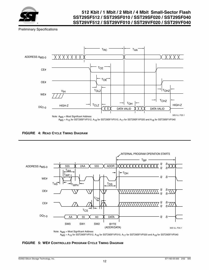
ReadThe Read operation of the SST29SFxxx and SST29VFxxxdevices are controlled by CE# and OE#, both have to below for the system to obtain data from the outputs. CE# isused for device selection. When CE# is high, the chip isdeselected and only standby power is consumed. OE# isthe output control and is used to gate data from the outputpins. The data bus is in high impedance state when eitherCE# or OE# is high. Refer to the Read cycle timing dia-gram for further details (Figure 4).
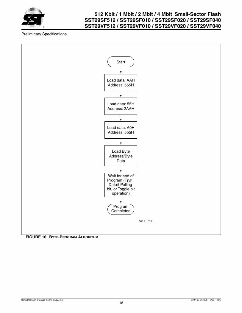
Byte-Program OperationThe SST29SFxxx and SST29VFxxx devices are pro-grammed on a byte-by-byte basis. Before programming,the sector where the byte exists must be fully erased. TheProgram operation is accomplished in three steps. The firststep is the three-byte load sequence for Software Data Pro-tection. The second step is to load byte address and bytedata. During the Byte-Program operation, the addressesare latched on the falling edge of either CE# or WE#,whichever occurs last. The data is latched on the risingedge of either CE# or WE#, whichever occurs first. Thethird step is the internal Program operation which is initi-ated after the rising edge of the fourth WE# or CE#, which-ever occurs first. The Program operation, once initiated, willbe completed, within 20 µs. See Figures 5 and 6 for WE#and CE# controlled Program operation timing diagramsand Figure 16 for flowcharts. During the Program opera-tion, the only valid reads are Data# Polling and Toggle Bit.During the internal Program operation, the host is free toperform additional tasks. Any commands written during theinternal Program operation will be ignored.
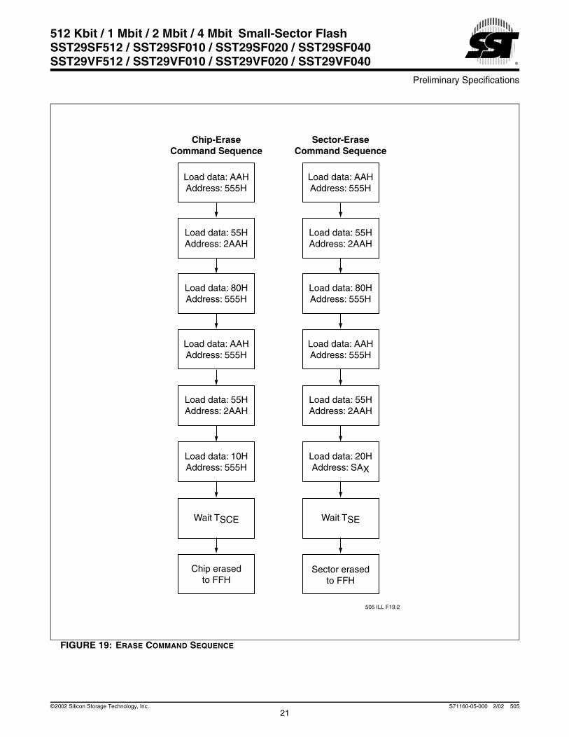
Sector-Erase OperationThe Sector-Erase operation allows the system to erase thedevice on a sector-by-sector basis. The SST29SFxxx andSST29VFxxx offer Sector-Erase mode. The sector archi-tecture is based on uniform sector size of 128 Bytes. TheSector-Erase operation is initiated by executing a six-byte-command sequence with Sector-Erase command (20H)and sector address (SA) in the last bus cycle. The sectoraddress is latched on the falling edge of the sixth WE#
pulse, while the command (20H) is latched on the risingedge of the sixth WE# pulse. The internal Erase operationbegins after the sixth WE# pulse. The End-of-Erase opera-tion can be determined using either Data# Polling or ToggleBit methods. See Figure 9 for timing waveforms. Any com-mands issued during the Sector-Erase operation areignored.
Chip-Erase OperationThe SST29SFxxx and SST29VFxxx devices provide aChip-Erase operation, which allows the user to erase theentire memory array to the “1s” state. This is useful whenthe entire device must be quickly erased.
The Chip-Erase operation is initiated by executing a six-byte Software Data Protection command sequence withChip-Erase command (10H) with address 555H in the lastbyte sequence. The internal Erase operation begins withthe rising edge of the sixth WE# or CE#, whichever occursfirst. During the internal Erase operation, the only valid readis Toggle Bit or Data# Polling. See Table 4 for the commandsequence, Figure 10 for timing diagram, and Figure 19 forthe flowchart. Any commands written during the Chip-Erase operation will be ignored.
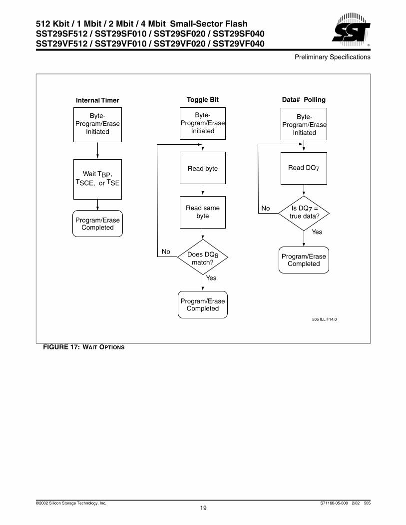
Write Operation Status DetectionThe SST29SFxxx and SST29VFxxx devices provide twosoftware means to detect the completion of a Write (Pro-gram or Erase) cycle, in order to optimize the systemWrite cycle time. The software detection includes twostatus bits: Data# Polling (DQ7) and Toggle Bit (DQ6).The End-of-Write detection mode is enabled after the ris-ing edge of WE# which initiates the internal Program orErase operation.
The actual completion of the nonvolatile write is asyn-chronous with the system; therefore, either a Data# Poll-ing or Toggle Bit read may be simultaneous with thecompletion of the Write cycle. If this occurs, the systemmay possibly get an erroneous result, i.e., valid data mayappear to conflict with either DQ7 or DQ6. In order to pre-vent spurious rejection, if an erroneous result occurs, thesoftware routine should include a loop to read theaccessed location an additional two (2) times. If bothreads are valid, then the device has completed the Writecycle, otherwise the rejection is valid.
2©2002 Silicon Storage Technology, Inc. S71160-05-000 2/02 505
Preliminary Specifications
512 Kbit / 1 Mbit / 2 Mbit / 4 Mbit Small-Sector FlashSST29SF512 / SST29SF010 / SST29SF020 / SST29SF040SST29VF512 / SST29VF010 / SST29VF020 / SST29VF040
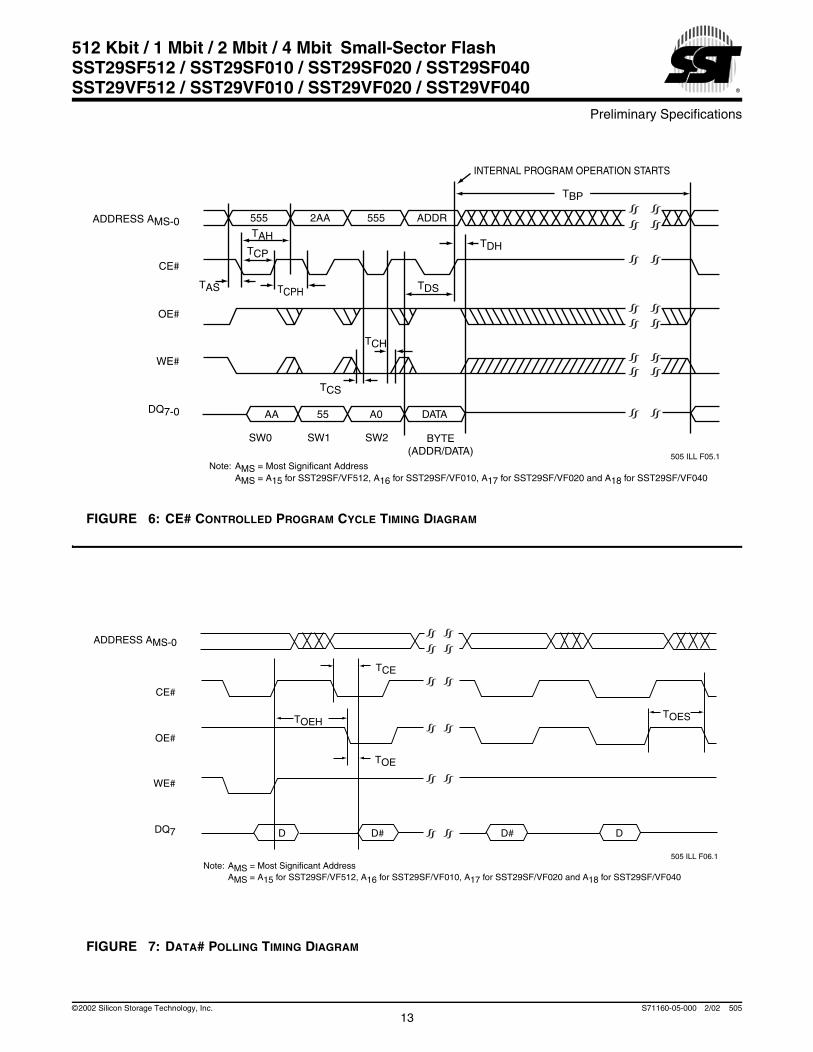
Data# Polling (DQ7)When the SST29SFxxx and SST29VFxxx devices are inthe internal Program operation, any attempt to read DQ7will produce the complement of the true data. Once theProgram operation is completed, DQ7 will produce truedata. Note that even though DQ7 may have valid dataimmediately following the completion of an internal Writeoperation, the remaining data outputs may still be invalid:valid data on the entire data bus will appear in subse-quent successive Read cycles after an interval of 1 µs.During internal Erase operation, any attempt to read DQ7will produce a ‘0’. Once the internal Erase operation iscompleted, DQ7 will produce a ‘1’. The Data# Polling isvalid after the rising edge of fourth WE# (or CE#) pulsefor Program operation. For Sector- or Chip-Erase, theData# Polling is valid after the rising edge of sixth WE#(or CE#) pulse. See Figure 7 for Data# Polling timing dia-gram and Figure 17 for a flowchart.
Toggle Bit (DQ6)During the internal Program or Erase operation, any con-secutive attempts to read DQ6 will produce alternating ‘0’sand ‘1’s, i.e., toggling between 0 and 1. When the internalProgram or Erase operation is completed, the toggling willstop. The device is then ready for the next operation. TheToggle Bit is valid after the rising edge of fourth WE# (orCE#) pulse for Program operation. For Sector or Chip-Erase, the Toggle Bit is valid after the rising edge of sixthWE# (or CE#) pulse. See Figure 8 for Toggle Bit timing dia-gram and Figure 17 for a flowchart.
Data ProtectionThe SST29SFxxx and SST29VFxxx devices provide bothhardware and software features to protect nonvolatile datafrom inadvertent writes.
Hardware Data ProtectionNoise/Glitch Protection: A WE# or CE# pulse of less than 5ns will not initiate a Write cycle.
VDD Power Up/Down Detection: The Write operation isinhibited when VDD is less than 2.5V for SST29SFxxx. TheWrite operation is inhibited when VDD is less than 1.5V. forSST29VFxxx.
Write Inhibit Mode: Forcing OE# low, CE# high, or WE#high will inhibit the Write operation. This prevents inadvert-ent writes during power-up or power-down.
Software Data Protection (SDP)The SST29SFxxx and SST29VFxxx provide the JEDECapproved Software Data Protection scheme for all dataalteration operations, i.e., Program and Erase. Any Pro-gram operation requires the inclusion of a series of three-byte sequence. The three-byte load sequence is used toinitiate the Program operation, providing optimal protectionfrom inadvertent Write operations, e.g., during the systempower-up or power-down. Any Erase operation requires theinclusion of a six-byte load sequence. These devices areshipped with the Software Data Protection permanentlyenabled. See Table 4 for the specific software commandcodes. During SDP command sequence, invalid com-mands will abort the device to read mode, within TRC.
3©2002 Silicon Storage Technology, Inc. S71160-05-000 2/02 505
Preliminary Specifications
512 Kbit / 1 Mbit / 2 Mbit / 4 Mbit Small-Sector FlashSST29SF512 / SST29SF010 / SST29SF020 / SST29SF040SST29VF512 / SST29VF010 / SST29VF020 / SST29VF040
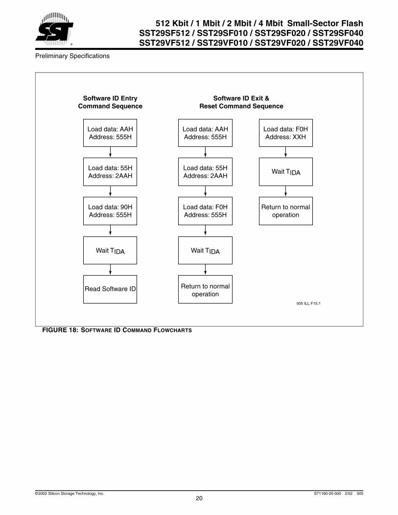
Product IdentificationThe Product Identification mode identifies the devices asSST29SF512, SST29SF010, SST29SF020, SST29SF040and SST29VF512, SST29VF010, SST29VF020,SST29VF040 and manufacturer as SST. This mode maybe accessed by software operations. Users may use theSoftware Product Identification operation to identify the part(i.e., using the device ID) when using multiple manufactur-ers in the same socket. For details, see Table 4 for softwareoperation, Figure 11 for the Software ID Entry and Readtiming diagram and Figure 18 for the Software ID Entrycommand sequence flowchart.
Product Identification Mode Exit/ResetIn order to return to the standard Read mode, the SoftwareProduct Identification mode must be exited. Exit is accom-plished by issuing the Software ID Exit commandsequence, which returns the device to the Read operation.Please note that the Software ID Exit command is ignoredduring an internal Program or Erase operation. See Table 4for software command codes, Figure 12 for timing wave-form, and Figure 18 for a flowchart.
TABLE 1: PRODUCT IDENTIFICATION
Address Data
Manufacturer’s ID 0000H BFH
Device ID
SST29SF512 0001H 20H
SST29VF512 0001H 21H
SST29SF010 0001H 22H
SST29VF010 0001H 23H
SST29SF020 0001H 24H
SST29VF020 0001H 25H
SST29SF040 0001H 13H
SST29VF040 0001H 14HT1.1 505
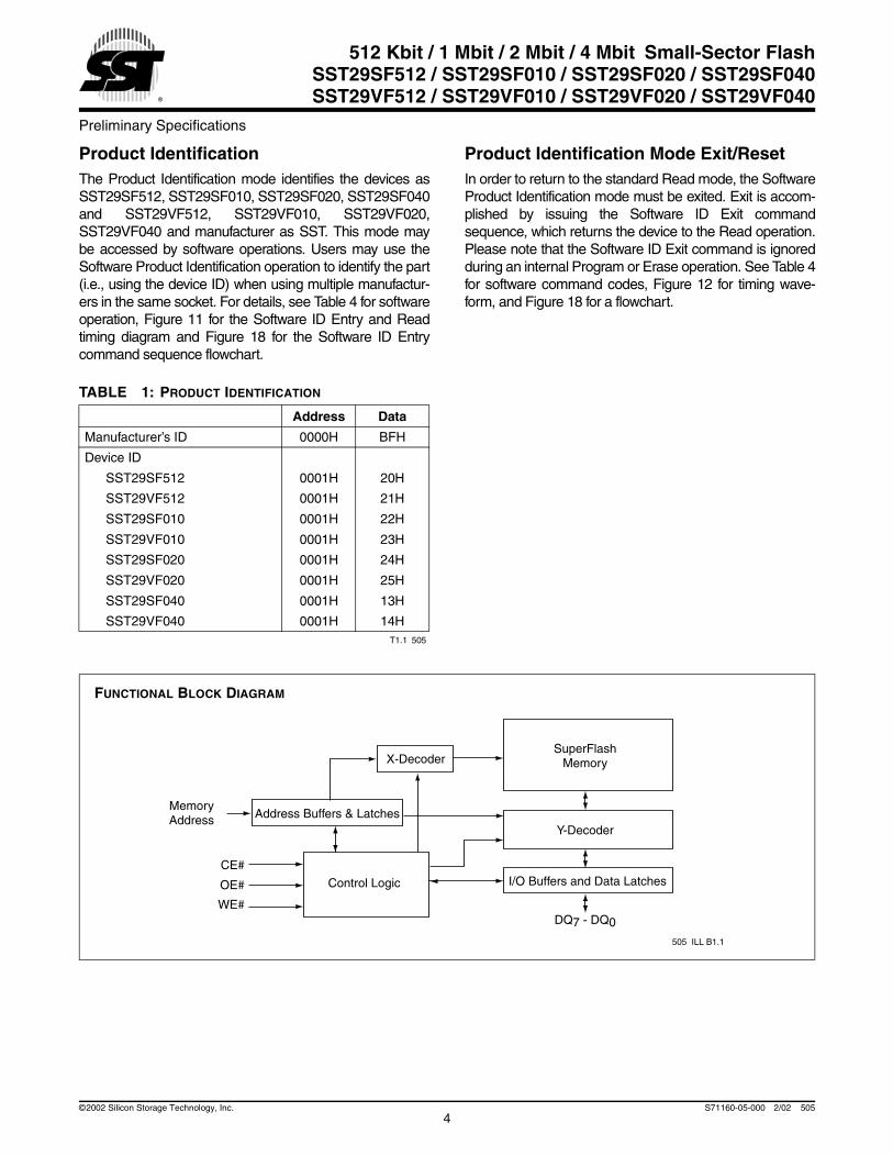
Y-Decoder
I/O Buffers and Data Latches
505 ILL B1.1
Address Buffers & Latches
X-Decoder
DQ7 - DQ0
MemoryAddress
OE#
CE#
WE#
SuperFlashMemory
Control Logic
FUNCTIONAL BLOCK DIAGRAM
4©2002 Silicon Storage Technology, Inc. S71160-05-000 2/02 505
Preliminary Specifications
512 Kbit / 1 Mbit / 2 Mbit / 4 Mbit Small-Sector FlashSST29SF512 / SST29SF010 / SST29SF020 / SST29SF040SST29VF512 / SST29VF010 / SST29VF020 / SST29VF040
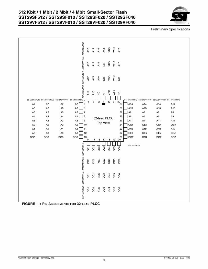
FIGURE 1: PIN ASSIGNMENTS FOR 32-LEAD PLCC
5
6
7
8
9
10
11
12
13
29
28
27
26
25
24
23
22
21
A7
A6
A5
A4
A3
A2
A1
A0
DQ0
A7
A6
A5
A4
A3
A2
A1
A0
DQ0
A7
A6
A5
A4
A3
A2
A1
A0
DQ0
A7
A6
A5
A4
A3
A2
A1
A0
DQ0
A14
A13
A8
A9
A11
OE#
A10
CE#
DQ7
A14
A13
A8
A9
A11
OE#
A10
CE#
DQ7
A14
A13
A8
A9
A11
OE#
A10
CE#
DQ7
A14
A13
A8
A9
A11
OE#
A10
CE#
DQ7
4 3 2 1 32 31 30
A12
A15
NC
NC
VD
D
WE
#
NC
A12
A15
A16
NC
VD
D
WE
#
NC
A12
A15
A16
NC
VD
D
WE
#
A17
A12
A15
A16
A18
VD
D
WE
#
A17
32-lead PLCCTop View
505 ILL F02a.4
14 15 16 17 18 19 20
DQ
1
DQ
2
VS
S
DQ
3
DQ
4
DQ
5
DQ
6
DQ
1
DQ
2
VS
S
DQ
3
DQ
4
DQ
5
DQ
6
DQ
1
DQ
2
VS
S
DQ
3
DQ
4
DQ
5
DQ
6
DQ
1
DQ
2
VS
S
DQ
3
DQ
4
DQ
5
DQ
6
SST29SF/VF512SST29SF/VF010SST29SF/VF020SST29SF/VF040 SST29SF/VF010 SST29SF/VF020 SST29SF/VF040SST29SF/VF512
SST2
9SF/
VF51
2SS
T29S
F/VF
010
SST2
9SF/
VF02
0SS
T29S
F/VF
040
SST2
9SF/
VF01
0SS
T29S
F/VF
020
SST2
9SF/
VF04
0SS
T29S
F/VF
512
5©2002 Silicon Storage Technology, Inc. S71160-05-000 2/02 505
Preliminary Specifications
512 Kbit / 1 Mbit / 2 Mbit / 4 Mbit Small-Sector FlashSST29SF512 / SST29SF010 / SST29SF020 / SST29SF040SST29VF512 / SST29VF010 / SST29VF020 / SST29VF040
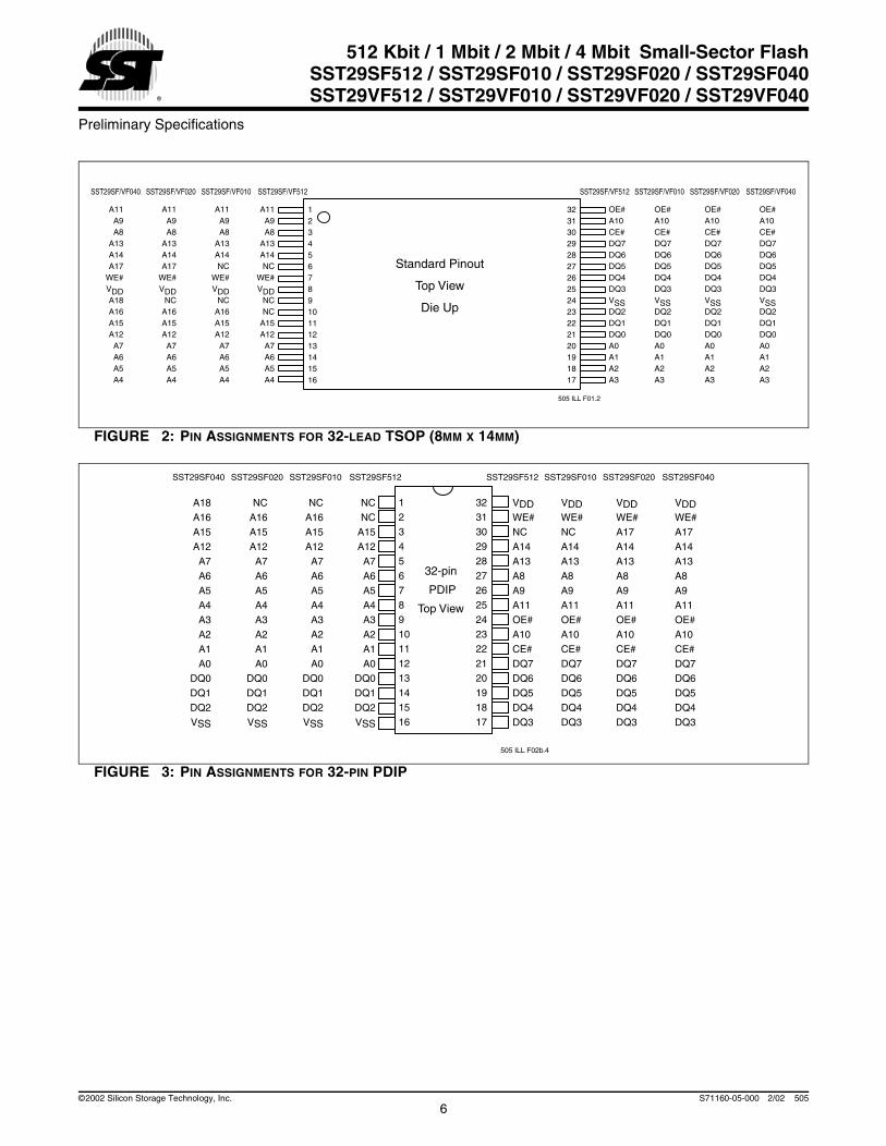
FIGURE 2: PIN ASSIGNMENTS FOR 32-LEAD TSOP (8MM X 14MM)
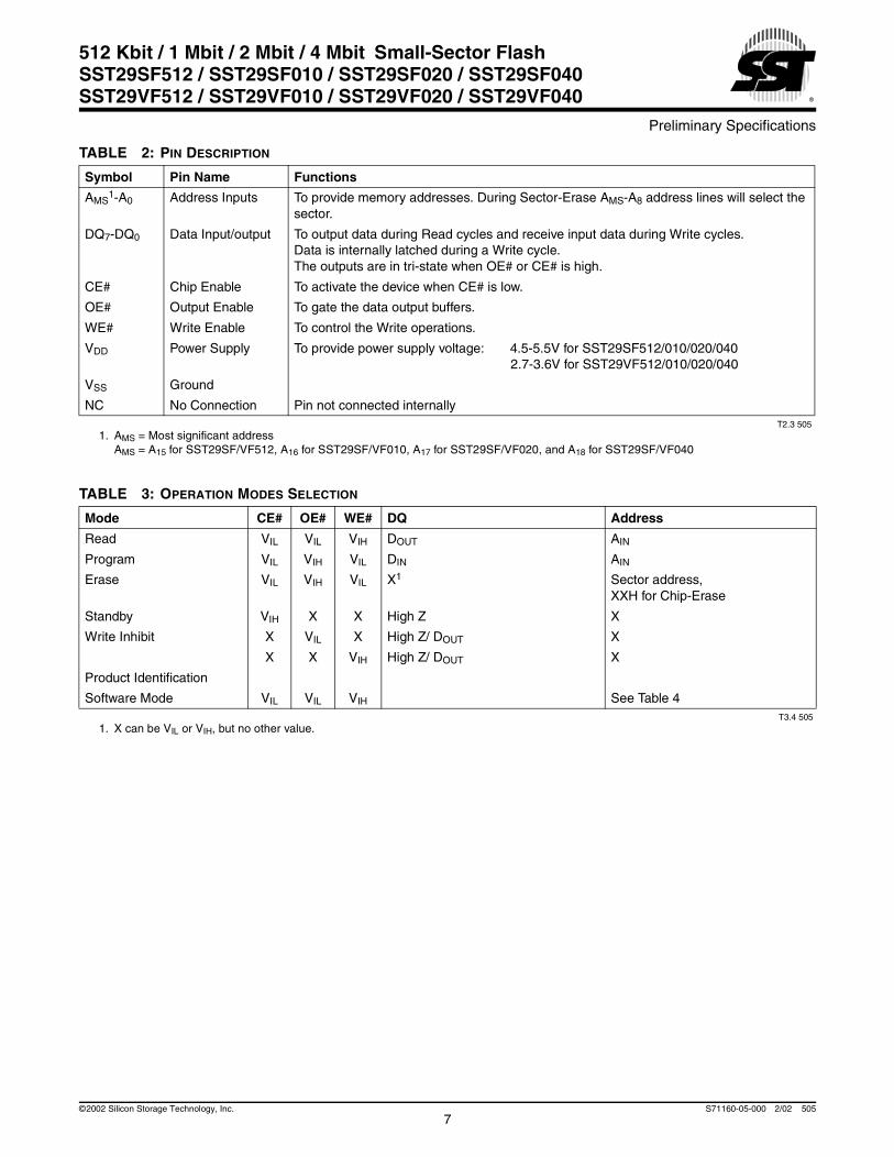
FIGURE 3: PIN ASSIGNMENTS FOR 32-PIN PDIP
A11A9A8
A13A14NC
WE#VDD
NCNC
A15A12A7A6A5A4
A11A9A8
A13A14NC
WE#VDD
NCA16A15A12A7A6A5A4
A11A9A8
A13A14A17
WE#VDD
NCA16A15A12A7A6A5A4
A11A9A8
A13A14A17
WE#VDDA18A16A15A12A7A6A5A4
SST29SF/VF512SST29SF/VF010SST29SF/VF020SST29SF/VF040 SST29SF/VF010 SST29SF/VF020 SST29SF/VF040SST29SF/VF512
12345678910111213141516
OE#A10CE#DQ7DQ6DQ5DQ4DQ3VSSDQ2DQ1DQ0A0A1A2A3
OE#A10CE#DQ7DQ6DQ5DQ4DQ3VSSDQ2DQ1DQ0A0A1A2A3
OE#A10CE#DQ7DQ6DQ5DQ4DQ3VSSDQ2DQ1DQ0A0A1A2A3
OE#A10CE#DQ7DQ6DQ5DQ4DQ3VSSDQ2DQ1DQ0A0A1A2A3
32313029282726252423222120191817
505 ILL F01.2
Standard Pinout
Top View
Die Up
12345678910111213141516
32-pin
PDIP
Top View
505 ILL F02b.4
NCNC
A15A12
A7A6A5A4A3A2A1A0
DQ0DQ1DQ2VSS
NCA16A15A12
A7A6A5A4A3A2A1A0
DQ0DQ1DQ2VSS
NCA16A15A12
A7A6A5A4A3A2A1A0
DQ0DQ1DQ2VSS
A18A16A15A12
A7A6A5A4A3A2A1A0
DQ0DQ1DQ2VSS
32313029282726252423222120191817
VDDWE#NCA14A13A8A9A11OE#A10CE#DQ7DQ6DQ5DQ4DQ3
VDDWE#NCA14A13A8A9A11OE#A10CE#DQ7DQ6DQ5DQ4DQ3
VDDWE#A17A14A13A8A9A11OE#A10CE#DQ7DQ6DQ5DQ4DQ3
VDDWE#A17A14A13A8A9A11OE#A10CE#DQ7DQ6DQ5DQ4DQ3
SST29SF512SST29SF010SST29SF020SST29SF040 SST29SF010 SST29SF020 SST29SF040SST29SF512
6©2002 Silicon Storage Technology, Inc. S71160-05-000 2/02 505
Preliminary Specifications
512 Kbit / 1 Mbit / 2 Mbit / 4 Mbit Small-Sector FlashSST29SF512 / SST29SF010 / SST29SF020 / SST29SF040SST29VF512 / SST29VF010 / SST29VF020 / SST29VF040
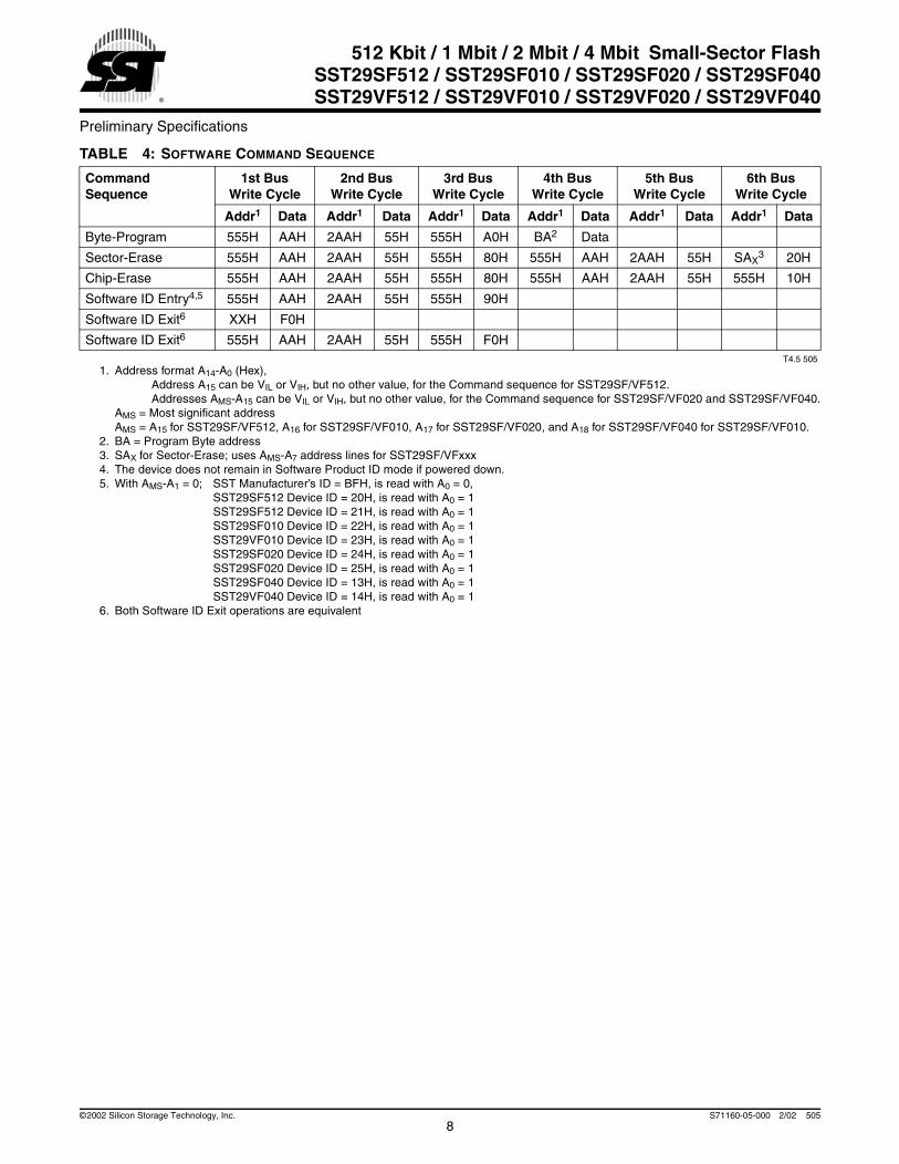
TABLE 2: PIN DESCRIPTION
Symbol Pin Name Functions
AMS1-A0 Address Inputs To provide memory addresses. During Sector-Erase AMS-A8 address lines will select the
sector.
DQ7-DQ0 Data Input/output To output data during Read cycles and receive input data during Write cycles.Data is internally latched during a Write cycle.The outputs are in tri-state when OE# or CE# is high.
CE# Chip Enable To activate the device when CE# is low.
OE# Output Enable To gate the data output buffers.
WE# Write Enable To control the Write operations.
VDD Power Supply To provide power supply voltage: 4.5-5.5V for SST29SF512/010/020/0402.7-3.6V for SST29VF512/010/020/040
VSS Ground
NC No Connection Pin not connected internallyT2.3 505
1. AMS = Most significant addressAMS = A15 for SST29SF/VF512, A16 for SST29SF/VF010, A17 for SST29SF/VF020, and A18 for SST29SF/VF040
TABLE 3: OPERATION MODES SELECTION
Mode CE# OE# WE# DQ Address
Read VIL VIL VIH DOUT AIN
Program VIL VIH VIL DIN AIN
Erase VIL VIH VIL X1
1. X can be VIL or VIH, but no other value.
Sector address,XXH for Chip-Erase
Standby VIH X X High Z X
Write Inhibit X VIL X High Z/ DOUT X
X X VIH High Z/ DOUT X
Product Identification
Software Mode VIL VIL VIH See Table 4T3.4 505
7©2002 Silicon Storage Technology, Inc. S71160-05-000 2/02 505
Preliminary Specifications
512 Kbit / 1 Mbit / 2 Mbit / 4 Mbit Small-Sector FlashSST29SF512 / SST29SF010 / SST29SF020 / SST29SF040SST29VF512 / SST29VF010 / SST29VF020 / SST29VF040
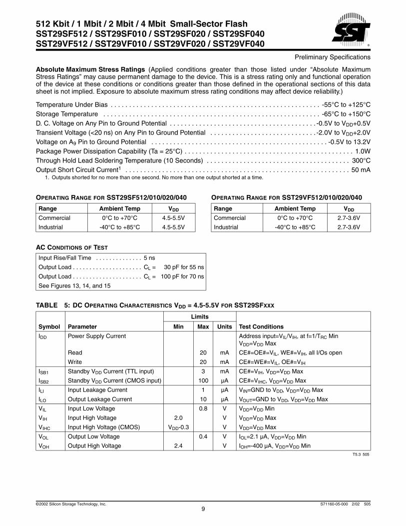
TABLE 4: SOFTWARE COMMAND SEQUENCE
CommandSequence
1st BusWrite Cycle
2nd BusWrite Cycle
3rd BusWrite Cycle
4th BusWrite Cycle
5th BusWrite Cycle
6th BusWrite Cycle
Addr1 Data Addr1 Data Addr1 Data Addr1 Data Addr1 Data Addr1 Data
Byte-Program 555H AAH 2AAH 55H 555H A0H BA2 Data
Sector-Erase 555H AAH 2AAH 55H 555H 80H 555H AAH 2AAH 55H SAX3 20H
Chip-Erase 555H AAH 2AAH 55H 555H 80H 555H AAH 2AAH 55H 555H 10H
Software ID Entry4,5 555H AAH 2AAH 55H 555H 90H
Software ID Exit6 XXH F0H
Software ID Exit6 555H AAH 2AAH 55H 555H F0HT4.5 505
1. Address format A14-A0 (Hex),Address A15 can be VIL or VIH, but no other value, for the Command sequence for SST29SF/VF512.Addresses AMS-A15 can be VIL or VIH, but no other value, for the Command sequence for SST29SF/VF020 and SST29SF/VF040.
AMS = Most significant addressAMS = A15 for SST29SF/VF512, A16 for SST29SF/VF010, A17 for SST29SF/VF020, and A18 for SST29SF/VF040 for SST29SF/VF010.
2. BA = Program Byte address3. SAX for Sector-Erase; uses AMS-A7 address lines for SST29SF/VFxxx4. The device does not remain in Software Product ID mode if powered down.5. With AMS-A1 = 0; SST Manufacturer’s ID = BFH, is read with A0 = 0,
SST29SF512 Device ID = 20H, is read with A0 = 1SST29SF512 Device ID = 21H, is read with A0 = 1SST29SF010 Device ID = 22H, is read with A0 = 1SST29VF010 Device ID = 23H, is read with A0 = 1SST29SF020 Device ID = 24H, is read with A0 = 1SST29SF020 Device ID = 25H, is read with A0 = 1SST29SF040 Device ID = 13H, is read with A0 = 1SST29VF040 Device ID = 14H, is read with A0 = 1
6. Both Software ID Exit operations are equivalent
8©2002 Silicon Storage Technology, Inc. S71160-05-000 2/02 505
Preliminary Specifications
512 Kbit / 1 Mbit / 2 Mbit / 4 Mbit Small-Sector FlashSST29SF512 / SST29SF010 / SST29SF020 / SST29SF040SST29VF512 / SST29VF010 / SST29VF020 / SST29VF040
Absolute Maximum Stress Ratings (Applied conditions greater than those listed under “Absolute MaximumStress Ratings” may cause permanent damage to the device. This is a stress rating only and functional operationof the device at these conditions or conditions greater than those defined in the operational sections of this datasheet is not implied. Exposure to absolute maximum stress rating conditions may affect device reliability.)
Temperature Under Bias . . . . . . . . . . . . . . . . . . . . . . . . . . . . . . . . . . . . . . . . . . . . . . . . . . . . . . . . . -55°C to +125°CStorage Temperature . . . . . . . . . . . . . . . . . . . . . . . . . . . . . . . . . . . . . . . . . . . . . . . . . . . . . . . . . . . -65°C to +150°CD. C. Voltage on Any Pin to Ground Potential . . . . . . . . . . . . . . . . . . . . . . . . . . . . . . . . . . . . . . . . -0.5V to VDD+0.5VTransient Voltage (<20 ns) on Any Pin to Ground Potential . . . . . . . . . . . . . . . . . . . . . . . . . . . . . -2.0V to VDD+2.0VVoltage on A9 Pin to Ground Potential . . . . . . . . . . . . . . . . . . . . . . . . . . . . . . . . . . . . . . . . . . . . . . . . -0.5V to 13.2VPackage Power Dissipation Capability (Ta = 25°C) . . . . . . . . . . . . . . . . . . . . . . . . . . . . . . . . . . . . . . . . . . . . . . 1.0WThrough Hold Lead Soldering Temperature (10 Seconds) . . . . . . . . . . . . . . . . . . . . . . . . . . . . . . . . . . . . . . . 300°COutput Short Circuit Current1 . . . . . . . . . . . . . . . . . . . . . . . . . . . . . . . . . . . . . . . . . . . . . . . . . . . . . . . . . . . . . 50 mA
1. Outputs shorted for no more than one second. No more than one output shorted at a time.
OPERATING RANGE FOR SST29SF512/010/020/040
Range Ambient Temp VDD
Commercial 0°C to +70°C 4.5-5.5V
Industrial -40°C to +85°C 4.5-5.5V
OPERATING RANGE FOR SST29VF512/010/020/040
Range Ambient Temp VDD
Commercial 0°C to +70°C 2.7-3.6V
Industrial -40°C to +85°C 2.7-3.6V
AC CONDITIONS OF TEST
Input Rise/Fall Time . . . . . . . . . . . . . . 5 ns
Output Load . . . . . . . . . . . . . . . . . . . . . CL = 30 pF for 55 ns
Output Load . . . . . . . . . . . . . . . . . . . . . CL = 100 pF for 70 ns
See Figures 13, 14, and 15
TABLE 5: DC OPERATING CHARACTERISTICS VDD = 4.5-5.5V FOR SST29SFXXX
Symbol Parameter
Limits
Test ConditionsMin Max Units
IDD Power Supply Current Address input=VIL/VIH, at f=1/TRC MinVDD=VDD Max
Read 20 mA CE#=OE#=VIL, WE#=VIH, all I/Os open
Write 20 mA CE#=WE#=VIL, OE#=VIH
ISB1 Standby VDD Current (TTL input) 3 mA CE#=VIH, VDD=VDD Max
ISB2 Standby VDD Current (CMOS input) 100 µA CE#=VIHC, VDD=VDD Max
ILI Input Leakage Current 1 µA VIN=GND to VDD, VDD=VDD Max
ILO Output Leakage Current 10 µA VOUT=GND to VDD, VDD=VDD Max
VIL Input Low Voltage 0.8 V VDD=VDD Min
VIH Input High Voltage 2.0 V VDD=VDD Max
VIHC Input High Voltage (CMOS) VDD-0.3 V VDD=VDD Max
VOL Output Low Voltage 0.4 V IOL=2.1 µA, VDD=VDD Min
VOH Output High Voltage 2.4 V IOH=-400 µA, VDD=VDD MinT5.3 505
9©2002 Silicon Storage Technology, Inc. S71160-05-000 2/02 505
Preliminary Specifications
512 Kbit / 1 Mbit / 2 Mbit / 4 Mbit Small-Sector FlashSST29SF512 / SST29SF010 / SST29SF020 / SST29SF040SST29VF512 / SST29VF010 / SST29VF020 / SST29VF040
TABLE 6: DC OPERATING CHARACTERISTICS VDD = 2.7-3.6V FOR SST29VFXXX
Symbol Parameter
Limits
Test ConditionsMin Max Units
IDD Power Supply Current Address input=VIL/VIH, at f=1/TRC MinVDD=VDD Max
Read 20 mA CE#=OE#=VIL, WE#=VIH, all I/Os open
Write 20 mA CE#=WE#=VIL, OE#=VIH
ISB Standby VDD Current 15 µA CE#=VIHC, VDD=VDD Max
ILI Input Leakage Current 1 µA VIN=GND to VDD, VDD=VDD Max
ILO Output Leakage Current 10 µA VOUT=GND to VDD, VDD=VDD Max
VIL Input Low Voltage 0.8 V VDD=VDD Min
VIH Input High Voltage 0.7VDD V VDD=VDD Max
VIHC Input High Voltage (CMOS) VDD-0.3 V VDD=VDD Max
VOL Output Low Voltage 0.2 V IOL=100 µA, VDD=VDD Min
VOH Output High Voltage VDD-0.2 V IOH=-100 µA, VDD=VDD MinT6.5 505
TABLE 7: RECOMMENDED SYSTEM POWER-UP TIMINGS
Symbol Parameter Minimum Units
TPU-READ1
1. This parameter is measured only for initial qualification and after a design or process change that could affect this parameter.
Power-up to Read Operation 100 µs
TPU-WRITE1 Power-up to Program/Erase Operation 100 µs
T7.1 505
TABLE 8: CAPACITANCE (Ta = 25°C, f=1 Mhz, other pins open)
Parameter Description Test Condition Maximum
CI/O1
1. This parameter is measured only for initial qualification and after a design or process change that could affect this parameter.
I/O Pin Capacitance VI/O = 0V 12 pF
CIN1 Input Capacitance VIN = 0V 6 pF
T8.1 505
TABLE 9: RELIABILITY CHARACTERISTICS
Symbol Parameter Minimum Specification Units Test Method
NEND1
1. This parameter is measured only for initial qualification and after a design or process change that could affect this parameter.
Endurance 10,000 Cycles JEDEC Standard A117
TDR1 Data Retention 100 Years JEDEC Standard A103
ILTH1 Latch Up 100 + IDD mA JEDEC Standard 78
T9.2 505
10©2002 Silicon Storage Technology, Inc. S71160-05-000 2/02 505
Preliminary Specifications
512 Kbit / 1 Mbit / 2 Mbit / 4 Mbit Small-Sector FlashSST29SF512 / SST29SF010 / SST29SF020 / SST29SF040SST29VF512 / SST29VF010 / SST29VF020 / SST29VF040
AC CHARACTERISTICS
TABLE 10: READ CYCLE TIMING PARAMETERS
VDD = 4.5-5.5V FOR SST29SFXXX AND 2.7-3.6V FOR SST29VFXXX
Symbol Parameter
SST29SF/VFxxx-55 SST29SF/VFxxx-70
UnitsMin Max Min Max
TRC Read Cycle Time 55 70 ns
TCE Chip Enable Access Time 55 70 ns
TAA Address Access Time 55 70 ns
TOE Output Enable Access Time 30 35 ns
TCLZ1
1. This parameter is measured only for initial qualification and after a design or process change that could affect this parameter.
CE# Low to Active Output 0 0 ns
TOLZ1 OE# Low to Active Output 0 0 ns
TCHZ1 CE# High to High-Z Output 20 25 ns
TOHZ1 OE# High to High-Z Output 20 25 ns
TOH1 Output Hold from Address Change 0 0 ns
T10.6 505
TABLE 11: PROGRAM/ERASE CYCLE TIMING PARAMETERS
VDD = 4.5-5.5V FOR SST29SFXXX AND 2.7-3.6V FOR SST29VFXXX
Symbol Parameter Min Max Units
TBP Byte-Program Time 20 µs
TAS Address Setup Time 0 ns
TAH Address Hold Time 30 ns
TCS WE# and CE# Setup Time 0 ns
TCH WE# and CE# Hold Time 0 ns
TOES OE# High Setup Time 0 ns
TOEH OE# High Hold Time 10 ns
TCP CE# Pulse Width 40 ns
TWP WE# Pulse Width 40 ns
TWPH1
1. This parameter is measured only for initial qualification and after a design or process change that could affect this parameter.
WE# Pulse Width High 30 ns
TCPH1 CE# Pulse Width High 30 ns
TDS Data Setup Time 40 ns
TDH1 Data Hold Time 0 ns
TIDA1 Software ID Access and Exit Time 150 ns
TSE Sector-Erase 25 ms
TSCE Chip-Erase 100 msT11.7 505
11©2002 Silicon Storage Technology, Inc. S71160-05-000 2/02 505
Preliminary Specifications
512 Kbit / 1 Mbit / 2 Mbit / 4 Mbit Small-Sector FlashSST29SF512 / SST29SF010 / SST29SF020 / SST29SF040SST29VF512 / SST29VF010 / SST29VF020 / SST29VF040
FIGURE 4: READ CYCLE TIMING DIAGRAM
FIGURE 5: WE# CONTROLLED PROGRAM CYCLE TIMING DIAGRAM
505 ILL F03.1
ADDRESS AMS-0
DQ7-0
WE#
OE#
CE#TCE
TRC TAA
TOE
TOLZVIH
HIGH-Z TCLZTOH
TCHZ
HIGH-ZDATA VALIDDATA VALID
TOHZ
Note: AMS = Most Significant AddressAMS = A15 for SST29SF/VF512, A16 for SST29SF/VF010, A17 for SST29SF/VF020 and A18 for SST29SF/VF040
505 ILL F04.1
ADDRESS AMS-0
DQ7-0
TDH
TWPHTDS
TWP
TAH
TAS
TCH
TCS
CE#
SW0 SW1 SW2
555 2AA 555 ADDR
AA 55 A0 DATA
INTERNAL PROGRAM OPERATION STARTS
BYTE(ADDR/DATA)
OE#
WE#
TBP
Note: AMS = Most Significant AddressAMS = A15 for SST29SF/VF512, A16 for SST29SF/VF010, A17 for SST29SF/VF020 and A18 for SST29SF/VF040
12©2002 Silicon Storage Technology, Inc. S71160-05-000 2/02 505
Preliminary Specifications
512 Kbit / 1 Mbit / 2 Mbit / 4 Mbit Small-Sector FlashSST29SF512 / SST29SF010 / SST29SF020 / SST29SF040SST29VF512 / SST29VF010 / SST29VF020 / SST29VF040
FIGURE 6: CE# CONTROLLED PROGRAM CYCLE TIMING DIAGRAM
FIGURE 7: DATA# POLLING TIMING DIAGRAM
505 ILL F05.1
ADDRESS AMS-0
DQ7-0
TDH
TCPHTDS
TCP
TAH
TAS
TCH
TCS
WE#
SW0 SW1 SW2
555 2AA 555 ADDR
AA 55 A0 DATA
INTERNAL PROGRAM OPERATION STARTS
BYTE(ADDR/DATA)
OE#
CE#
TBP
Note: AMS = Most Significant AddressAMS = A15 for SST29SF/VF512, A16 for SST29SF/VF010, A17 for SST29SF/VF020 and A18 for SST29SF/VF040
505 ILL F06.1
ADDRESS AMS-0
DQ7 D D# D# D
WE#
OE#
CE#
TOEH
TOE
TCE
TOES
Note: AMS = Most Significant AddressAMS = A15 for SST29SF/VF512, A16 for SST29SF/VF010, A17 for SST29SF/VF020 and A18 for SST29SF/VF040
13©2002 Silicon Storage Technology, Inc. S71160-05-000 2/02 505
Preliminary Specifications
512 Kbit / 1 Mbit / 2 Mbit / 4 Mbit Small-Sector FlashSST29SF512 / SST29SF010 / SST29SF020 / SST29SF040SST29VF512 / SST29VF010 / SST29VF020 / SST29VF040
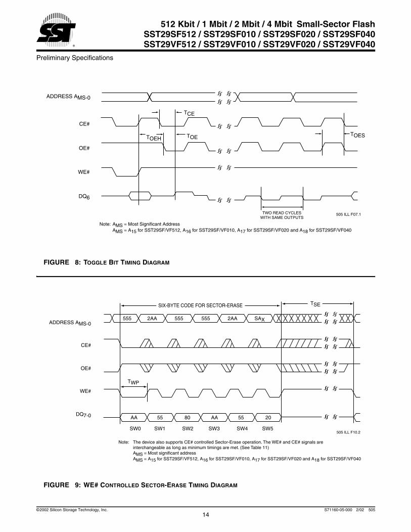
FIGURE 8: TOGGLE BIT TIMING DIAGRAM
FIGURE 9: WE# CONTROLLED SECTOR-ERASE TIMING DIAGRAM
505 ILL F07.1
ADDRESS AMS-0
DQ6
WE#
OE#
CE#
TOETOEH
TCE
TOES
TWO READ CYCLESWITH SAME OUTPUTS
Note: AMS = Most Significant AddressAMS = A15 for SST29SF/VF512, A16 for SST29SF/VF010, A17 for SST29SF/VF020 and A18 for SST29SF/VF040
505 ILL F10.2
ADDRESS AMS-0
DQ7-0
WE#
SW0 SW1 SW2 SW3 SW4 SW5
555 2AA 2AA555 555
55 2055AA 80 AA
SAX
OE#
CE#
SIX-BYTE CODE FOR SECTOR-ERASE TSE
TWP
Note: The device also supports CE# controlled Sector-Erase operation. The WE# and CE# signals areinterchangeable as long as minimum timings are met. (See Table 11)AMS = Most significant addressAMS = A15 for SST29SF/VF512, A16 for SST29SF/VF010, A17 for SST29SF/VF020 and A18 for SST29SF/VF040
14©2002 Silicon Storage Technology, Inc. S71160-05-000 2/02 505
Preliminary Specifications
512 Kbit / 1 Mbit / 2 Mbit / 4 Mbit Small-Sector FlashSST29SF512 / SST29SF010 / SST29SF020 / SST29SF040SST29VF512 / SST29VF010 / SST29VF020 / SST29VF040
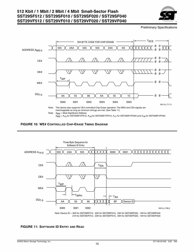
FIGURE 10: WE# CONTROLLED CHIP-ERASE TIMING DIAGRAM
FIGURE 11: SOFTWARE ID ENTRY AND READ
505 ILL F17.2
ADDRESS AMS-0
DQ7-0
WE#
SW0 SW1 SW2 SW3 SW4 SW5
555 2AA 2AA555 555
55 1055AA 80 AA
555
OE#
CE#
SIX-BYTE CODE FOR CHIP-ERASE TSCE
TWP
Note: This device also supports CE# controlled Chip-Erase operation. The WE# and CE# signals areinterchageable as long as minimum timings are met. (See Table 11)
Note: AMS = Most Significant AddressAMS = A15 for SST29SF/VF512, A16 for SST29SF/VF010, A17 for SST29SF/VF020 and A18 for SST29SF/VF040
505 ILL F08.2
ADDRESS A14-0
DQ7-0
WE#
Note: Device ID = 20H for SST29SF512, 22H for SST29SF010, 24H for SST29SF020, 13H for SST29SF04021H for SST29VF512, 23H for SST29VF010, 25H for SST29VF020, 14H for SST29VF040
SW1SW0 SW2
Device ID
555 2AA 555 0000 0001
OE#
CE#
Three-Byte Sequence for Software ID Entry
TWP
TWPH TAA
BF55AA 90
TIDA
15©2002 Silicon Storage Technology, Inc. S71160-05-000 2/02 505
Preliminary Specifications
512 Kbit / 1 Mbit / 2 Mbit / 4 Mbit Small-Sector FlashSST29SF512 / SST29SF010 / SST29SF020 / SST29SF040SST29VF512 / SST29VF010 / SST29VF020 / SST29VF040
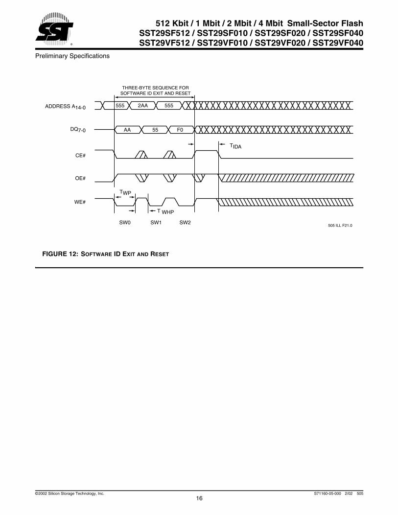
FIGURE 12: SOFTWARE ID EXIT AND RESET
505 ILL F21.0
ADDRESS A14-0
DQ7-0
TIDA
TWP
T WHP
WE#
SW0 SW1 SW2
555 2AA 555
THREE-BYTE SEQUENCE FORSOFTWARE ID EXIT AND RESET
OE#
CE#
AA 55 F0
16©2002 Silicon Storage Technology, Inc. S71160-05-000 2/02 505
Preliminary Specifications
512 Kbit / 1 Mbit / 2 Mbit / 4 Mbit Small-Sector FlashSST29SF512 / SST29SF010 / SST29SF020 / SST29SF040SST29VF512 / SST29VF010 / SST29VF020 / SST29VF040
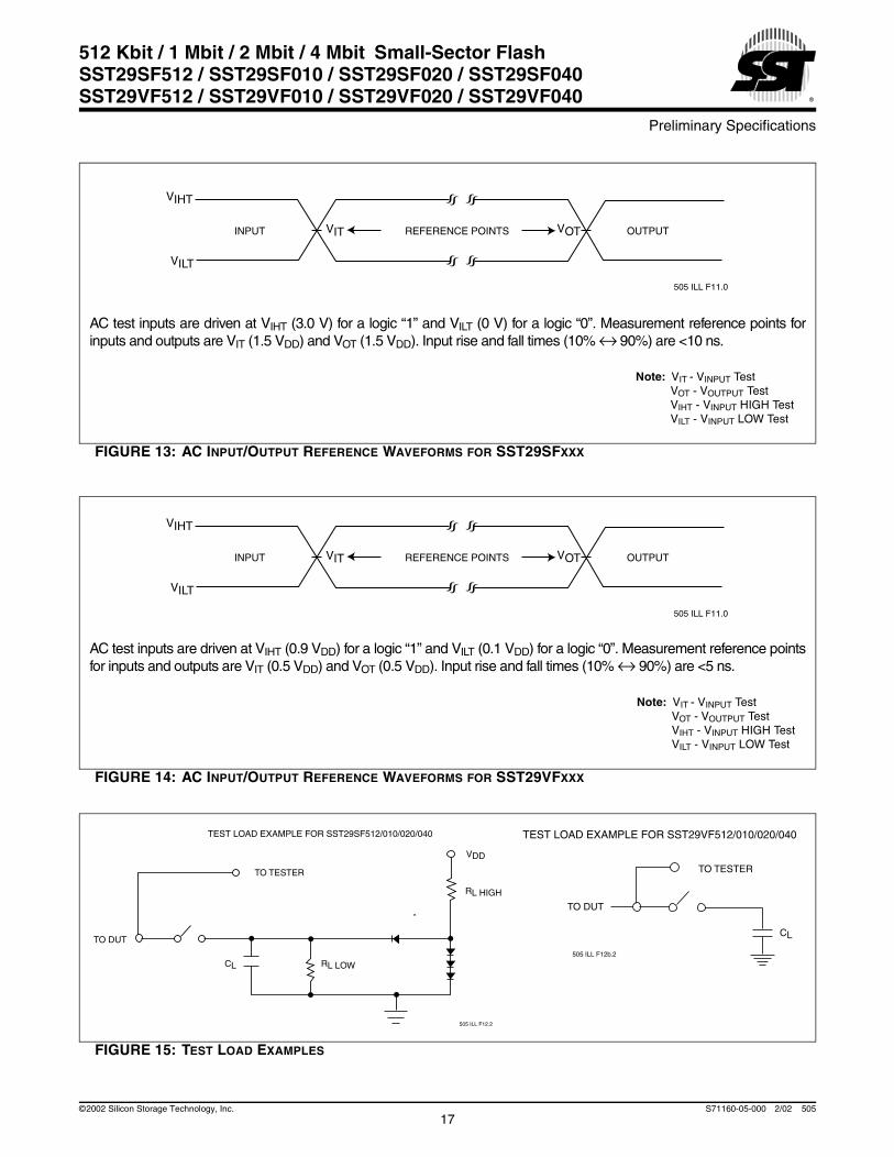
FIGURE 13: AC INPUT/OUTPUT REFERENCE WAVEFORMS FOR SST29SFXXX
FIGURE 14: AC INPUT/OUTPUT REFERENCE WAVEFORMS FOR SST29VFXXX
FIGURE 15: TEST LOAD EXAMPLES
505 ILL F11.0
REFERENCE POINTS OUTPUTINPUT VIT
VIHT
VILT
VOT
AC test inputs are driven at VIHT (3.0 V) for a logic “1” and VILT (0 V) for a logic “0”. Measurement reference points forinputs and outputs are VIT (1.5 VDD) and VOT (1.5 VDD). Input rise and fall times (10% ↔ 90%) are <10 ns.
Note: VIT - VINPUT TestVOT - VOUTPUT TestVIHT - VINPUT HIGH TestVILT - VINPUT LOW Test
505 ILL F11.0
REFERENCE POINTS OUTPUTINPUT VIT
VIHT
VILT
VOT
AC test inputs are driven at VIHT (0.9 VDD) for a logic “1” and VILT (0.1 VDD) for a logic “0”. Measurement reference pointsfor inputs and outputs are VIT (0.5 VDD) and VOT (0.5 VDD). Input rise and fall times (10% ↔ 90%) are <5 ns.
Note: VIT - VINPUT TestVOT - VOUTPUT TestVIHT - VINPUT HIGH TestVILT - VINPUT LOW Test
505 ILL F12b.2
TO TESTER
TO DUT
CL
TEST LOAD EXAMPLE FOR SST29VF512/010/020/040
505 ILL F12.2
TEST LOAD EXAMPLE FOR SST29SF512/010/020/040
TO TESTER
TO DUT
CL RL LOW
RL HIGH
VDD
17©2002 Silicon Storage Technology, Inc. S71160-05-000 2/02 505
Preliminary Specifications
512 Kbit / 1 Mbit / 2 Mbit / 4 Mbit Small-Sector FlashSST29SF512 / SST29SF010 / SST29SF020 / SST29SF040SST29VF512 / SST29VF010 / SST29VF020 / SST29VF040
FIGURE 16: BYTE-PROGRAM ALGORITHM
505 ILL F13.1
Start
Load data: AAHAddress: 555H
Load data: 55HAddress: 2AAH
Load data: A0HAddress: 555H
Load ByteAddress/Byte
Data
Wait for end ofProgram (TBP,Data# Polling
bit, or Toggle bitoperation)
ProgramCompleted
18©2002 Silicon Storage Technology, Inc. S71160-05-000 2/02 505
Preliminary Specifications
512 Kbit / 1 Mbit / 2 Mbit / 4 Mbit Small-Sector FlashSST29SF512 / SST29SF010 / SST29SF020 / SST29SF040SST29VF512 / SST29VF010 / SST29VF020 / SST29VF040
FIGURE 17: WAIT OPTIONS
505 ILL F14.0
Wait TBP,TSCE, or TSE
Byte-Program/Erase
Initiated
Internal Timer Toggle Bit
Yes
Yes
No
No
Program/EraseCompleted
Does DQ6match?
Read samebyte
Data# Polling
Program/EraseCompleted
Program/EraseCompleted
Read byte
Is DQ7 =true data?
Read DQ7
Byte-Program/Erase
Initiated
Byte-Program/Erase
Initiated
19©2002 Silicon Storage Technology, Inc. S71160-05-000 2/02 505
Preliminary Specifications
512 Kbit / 1 Mbit / 2 Mbit / 4 Mbit Small-Sector FlashSST29SF512 / SST29SF010 / SST29SF020 / SST29SF040SST29VF512 / SST29VF010 / SST29VF020 / SST29VF040
FIGURE 18: SOFTWARE ID COMMAND FLOWCHARTS
505 ILL F15.1
Load data: AAHAddress: 555H
Software ID EntryCommand Sequence
Load data: 55HAddress: 2AAH
Load data: 90HAddress: 555H
Wait TIDA
Read Software ID
Load data: AAHAddress: 555H
Software ID Exit &Reset Command Sequence
Load data: 55HAddress: 2AAH
Load data: F0HAddress: 555H
Load data: F0HAddress: XXH
Return to normaloperation
Wait TIDA
Wait TIDA
Return to normaloperation
20©2002 Silicon Storage Technology, Inc. S71160-05-000 2/02 505
Preliminary Specifications
512 Kbit / 1 Mbit / 2 Mbit / 4 Mbit Small-Sector FlashSST29SF512 / SST29SF010 / SST29SF020 / SST29SF040SST29VF512 / SST29VF010 / SST29VF020 / SST29VF040
FIGURE 19: ERASE COMMAND SEQUENCE
505 ILL F19.2
Load data: AAHAddress: 555H
Chip-EraseCommand Sequence
Load data: 55HAddress: 2AAH
Load data: 80HAddress: 555H
Load data: 55HAddress: 2AAH
Load data: 10HAddress: 555H
Load data: AAHAddress: 555H
Wait TSCE
Chip erasedto FFH
Load data: AAHAddress: 555H
Sector-EraseCommand Sequence
Load data: 55HAddress: 2AAH
Load data: 80HAddress: 555H
Load data: 55HAddress: 2AAH
Load data: 20HAddress: SAX
Load data: AAHAddress: 555H
Wait TSE
Sector erasedto FFH
21©2002 Silicon Storage Technology, Inc. S71160-05-000 2/02 505
Preliminary Specifications
512 Kbit / 1 Mbit / 2 Mbit / 4 Mbit Small-Sector FlashSST29SF512 / SST29SF010 / SST29SF020 / SST29SF040SST29VF512 / SST29VF010 / SST29VF020 / SST29VF040
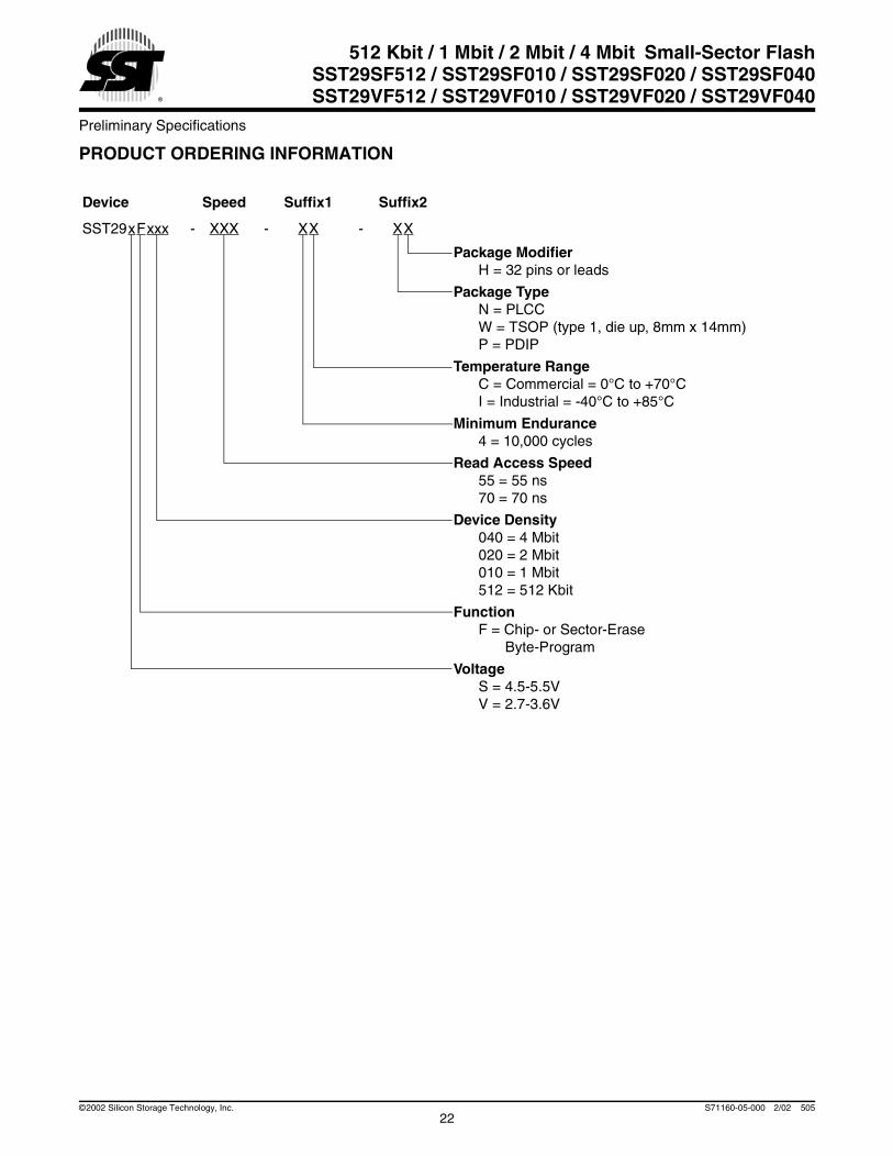
PRODUCT ORDERING INFORMATION
Device Speed Suffix1 Suffix2
SST29xFxxx - XXX - XX - XX
Package ModifierH = 32 pins or leads
Package TypeN = PLCCW = TSOP (type 1, die up, 8mm x 14mm)P = PDIP
Temperature RangeC = Commercial = 0°C to +70°CI = Industrial = -40°C to +85°C
Minimum Endurance4 = 10,000 cycles
Read Access Speed55 = 55 ns70 = 70 ns
Device Density040 = 4 Mbit020 = 2 Mbit010 = 1 Mbit512 = 512 Kbit
FunctionF = Chip- or Sector-Erase
Byte-Program
VoltageS = 4.5-5.5VV = 2.7-3.6V
22©2002 Silicon Storage Technology, Inc. S71160-05-000 2/02 505
Preliminary Specifications
512 Kbit / 1 Mbit / 2 Mbit / 4 Mbit Small-Sector FlashSST29SF512 / SST29SF010 / SST29SF020 / SST29SF040SST29VF512 / SST29VF010 / SST29VF020 / SST29VF040
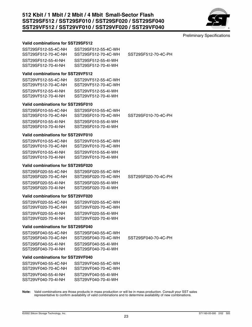
Valid combinations for SST29SF512
SST29SF512-55-4C-NH SST29SF512-55-4C-WHSST29SF512-70-4C-NH SST29SF512-70-4C-WH SST29SF512-70-4C-PH
SST29SF512-55-4I-NH SST29SF512-55-4I-WHSST29SF512-70-4I-NH SST29SF512-70-4I-WH
Valid combinations for SST29VF512
SST29VF512-55-4C-NH SST29VF512-55-4C-WHSST29VF512-70-4C-NH SST29VF512-70-4C-WH
SST29VF512-55-4I-NH SST29VF512-55-4I-WHSST29VF512-70-4I-NH SST29VF512-70-4I-WH
Valid combinations for SST29SF010
SST29SF010-55-4C-NH SST29SF010-55-4C-WHSST29SF010-70-4C-NH SST29SF010-70-4C-WH SST29SF010-70-4C-PH
SST29SF010-55-4I-NH SST29SF010-55-4I-WHSST29SF010-70-4I-NH SST29SF010-70-4I-WH
Valid combinations for SST29VF010
SST29VF010-55-4C-NH SST29VF010-55-4C-WHSST29VF010-70-4C-NH SST29VF010-70-4C-WH
SST29VF010-55-4I-NH SST29VF010-55-4I-WHSST29VF010-70-4I-NH SST29VF010-70-4I-WH
Valid combinations for SST29SF020
SST29SF020-55-4C-NH SST29SF020-55-4C-WHSST29SF020-70-4C-NH SST29SF020-70-4C-WH SST29SF020-70-4C-PH
SST29SF020-55-4I-NH SST29SF020-55-4I-WHSST29SF020-70-4I-NH SST29SF020-70-4I-WH
Valid combinations for SST29VF020
SST29VF020-55-4C-NH SST29VF020-55-4C-WHSST29VF020-70-4C-NH SST29VF020-70-4C-WH
SST29VF020-55-4I-NH SST29VF020-55-4I-WHSST29VF020-70-4I-NH SST29VF020-70-4I-WH
Valid combinations for SST29SF040
SST29SF040-55-4C-NH SST29SF040-55-4C-WHSST29SF040-70-4C-NH SST29SF040-70-4C-WH SST29SF040-70-4C-PH
SST29SF040-55-4I-NH SST29SF040-55-4I-WHSST29SF040-70-4I-NH SST29SF040-70-4I-WH
Valid combinations for SST29VF040
SST29VF040-55-4C-NH SST29VF040-55-4C-WHSST29VF040-70-4C-NH SST29VF040-70-4C-WH
SST29VF040-55-4I-NH SST29VF040-55-4I-WHSST29VF040-70-4I-NH SST29VF040-70-4I-WH
Note: Valid combinations are those products in mass production or will be in mass production. Consult your SST sales representative to confirm availability of valid combinations and to determine availability of new combinations.
23©2002 Silicon Storage Technology, Inc. S71160-05-000 2/02 505
Preliminary Specifications
512 Kbit / 1 Mbit / 2 Mbit / 4 Mbit Small-Sector FlashSST29SF512 / SST29SF010 / SST29SF020 / SST29SF040SST29VF512 / SST29VF010 / SST29VF020 / SST29VF040
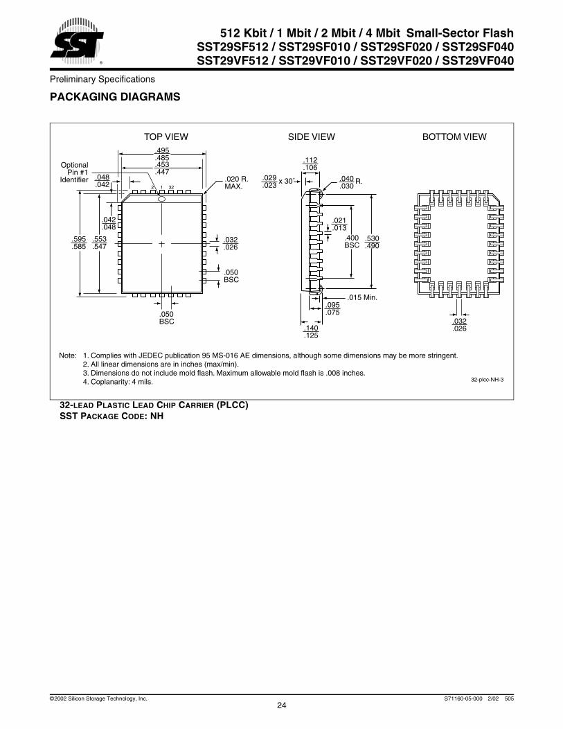
PACKAGING DIAGRAMS
32-LEAD PLASTIC LEAD CHIP CARRIER (PLCC)SST PACKAGE CODE: NH
.040
.030
.021
.013.530.490
.095
.075
.140
.125
.032
.026
.032
.026
.029
.023
.453
.447
.553
.547.595.585
.495
.485 .112.106
.042
.048
.048
.042
.015 Min.
TOP VIEW SIDE VIEW BOTTOM VIEW
12 32
.400BSC
32-plcc-NH-3
Note: 1. Complies with JEDEC publication 95 MS-016 AE dimensions, although some dimensions may be more stringent.2. All linear dimensions are in inches (max/min).3. Dimensions do not include mold flash. Maximum allowable mold flash is .008 inches.4. Coplanarity: 4 mils.
.050BSC
.050BSC
OptionalPin #1
Identifier .020 R.MAX.
R.x 30˚
24©2002 Silicon Storage Technology, Inc. S71160-05-000 2/02 505
Preliminary Specifications
512 Kbit / 1 Mbit / 2 Mbit / 4 Mbit Small-Sector FlashSST29SF512 / SST29SF010 / SST29SF020 / SST29SF040SST29VF512 / SST29VF010 / SST29VF020 / SST29VF040
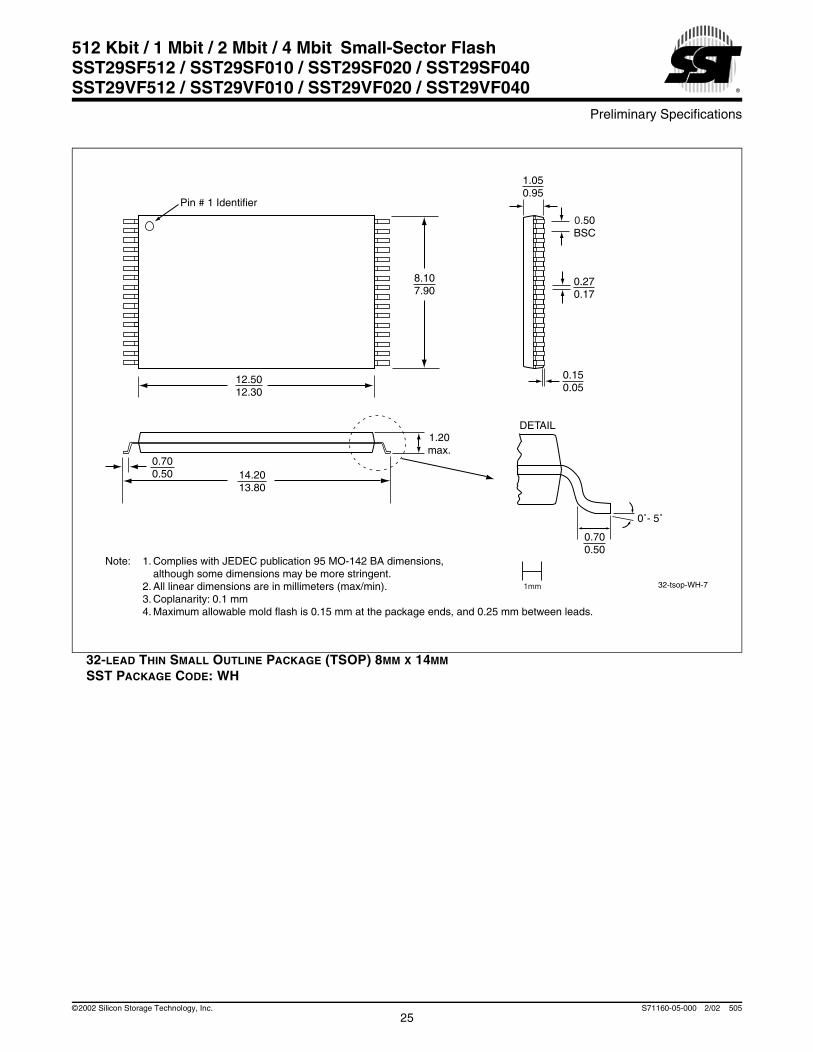
32-LEAD THIN SMALL OUTLINE PACKAGE (TSOP) 8MM X 14MM
SST PACKAGE CODE: WH
32-tsop-WH-7
Note: 1. Complies with JEDEC publication 95 MO-142 BA dimensions,although some dimensions may be more stringent.
2. All linear dimensions are in millimeters (max/min).3. Coplanarity: 0.1 mm4. Maximum allowable mold flash is 0.15 mm at the package ends, and 0.25 mm between leads.
1.20max.
1mm
Pin # 1 Identifier
12.5012.30
14.2013.80
0.700.50
8.107.90
0.270.17
0.50BSC
1.050.95
0.150.05
0.700.50
0˚- 5˚
DETAIL
25©2002 Silicon Storage Technology, Inc. S71160-05-000 2/02 505
Preliminary Specifications
512 Kbit / 1 Mbit / 2 Mbit / 4 Mbit Small-Sector FlashSST29SF512 / SST29SF010 / SST29SF020 / SST29SF040SST29VF512 / SST29VF010 / SST29VF020 / SST29VF040
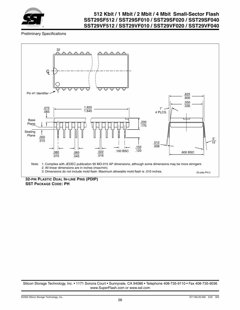
32-PIN PLASTIC DUAL IN-LINE PINS (PDIP)SST PACKAGE CODE: PH
32-pdip-PH-3
Pin #1 Identifier
CL
32
1
BasePlane
SeatingPlane
Note: 1. Complies with JEDEC publication 95 MO-015 AP dimensions, although some dimensions may be more stringent.2. All linear dimensions are in inches (max/min).3. Dimensions do not include mold flash. Maximum allowable mold flash is .010 inches.
.200
.170
7˚4 PLCS.
.600 BSC.100 BSC.150.120.022
.016.065.045
.080
.070
.050
.015
.075
.0651.6551.645
.012
.008
0˚15˚
.625
.600
.550
.530
Silicon Storage Technology, Inc. • 1171 Sonora Court • Sunnyvale, CA 94086 • Telephone 408-735-9110 • Fax 408-735-9036www.SuperFlash.com or www.sst.com
26©2002 Silicon Storage Technology, Inc. S71160-05-000 2/02 505