Embed Size (px)
Citation preview

5.1 Finite Difference Time Domain Technique (FDTD)
5.2 Theoretical analysis of cross patch antenna
5.3 Theoretical analysis of cross patch antenna with X-slot
5.4 Theoretical analysis of Frequency reconfigurable polarization diversity microstrip antenna
5.5 Chapter Summary
This chapter highlights a systematic approach to analyze a cross patch
antenna using FDTD based numerical computation. The staircase
approximation is employed to derive the slant edges of the X-slot. Various
steps involved in the extraction of antenna parameters along with the
assumptions taken in the implementation of the algorithm are also described.
The predicted results are experimentally verified by developing and testing
different printed cross patch antennas.
Co
nte
nts
Chapter-5
Department of Electronics, CUSAT 170
5.1 Finite Difference Time Domain Technique (FDTD)
Finite Difference Time Domain (FDTD) is a Computational Electro-Magnetic (CEM) technique that directly solves the differential form of Maxwell’s curl equations, in the time domain using a discretized space-time grid. Field, voltage or current samples are taken from fixed points in the FDTD grid and Fast Fourier Transform (FFT) is employed to compute the frequency domain information. Finite Difference Time Domain (FDTD) method was introduced by Yee [1] in 1966 for solving Maxwell’s curl equations directly in the time domain on a space grid. The algorithm was based on a central difference solution of Maxwell’s equations with spatially staggered electric and magnetic fields placed alternatively at each time steps in a leap-frog algorithm. This method has been implemented by Teflove in 1975 for the solution of complex inhomogeneous problems.
The FDTD has been used by many investigators, because of its following advantages over other techniques:
From the mathematical point of view, it is a direct implementation of Maxwell’s curl equations.
Broadband frequency response can be easily predicted since the analysis is carried out in the time domain.
Arbitrary, irregular geometries, wires of any thickness can be easily modeled,
It is capable of analyzing structures having different types of materials
Time histories of electric and magnetic fields throughout the entire simulation domain are available
Impedance and radiation pattern are easily obtainable
Lumped loads can be easily included in the model
Formulation of the FDTD method begins by considering the differential form of Maxwell’s two curl equations which govern the propagation of fields in
Theoretical Analysis of Cross Patch Antenna
Design and Development of Reconfigurable Compact Cross Patch Antenna for Switchable Polarization 171
the structures. For simplicity, the media is assumed to be uniform, isotropic, homogeneous and lossless.
With these assumptions, Maxwell’s equations can be written as
)1(..............................EyH
×−∇=∂∂µ
)2......(........................................HtE
×∇=∂∂ε
In order to find an approximate solution to these set of equations, the problem is discretized over a finite three dimensional computational domain with appropriate boundary conditions enforced on the source, conductors, and mesh walls. The divergence equations are automatically satisfied by the FDTD method.
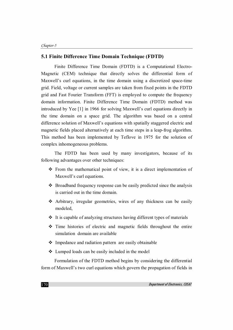
To obtain discrete approximations to these continuous partial differential equations the centered difference approximation is used on both time and space. For convenience, the six field locations are considered to be interleaved in space as shown in Fig. 5.1 which is a drawing of the FDTD unit cell. The entire computational domain is obtained by stacking these Yee cubes into a larger rectangular volume. The x, y and z dimensions of the unit cell are ∆x, ∆y and ∆z, respectively. The advantages of this field arrangement are that centered differences are realized in the calculation of each field component and that continuity of tangential field components is automatically satisfied.
Figure 5. 1 Yee Cell using in FDTD with Electric and Magnetic field
components

Chapter-5
Department of Electronics, CUSAT 172
Because there are only six unique field components within the unit cell,
the six field components touching the shaded upper eighth of the unit cell in
figure 5.1 are considered to be a unit node with subscript indices i, j, and k
corresponding to the node numbers in the x, y and z directions. The notation
implicitly assumes the ±1/2 space indices and thus simplifies the notation,
rendering the formulas directly implementable on the computer.
The time steps are indicated with the superscript n. Using this field
component arrangement, the above notation, and the centered difference
approximation, the explicit finite difference approximations to (1) and (2) are
( ) ( ) )3.....(..........,1,,,,,1,,,,,,2/1,,,
2/1,,, EEEEHH n
kjizn
kjizn
kjiyn
kjiyn
kjixn
kjix yt
zt
−−
−+ −∆∆
−−∆∆
+=µµ
( ) ( ) )4.........(..........1,,,,,,,,1,,,,2/1,,,
2/1,,, EEEEHH n
kjixn
kjixn
kjizn
kjizn
kjiyn
kjiy zt
xt
−−
−+ −∆∆
−−∆∆
+=µµ
( ) ( ) )5.......(..........,,1,,,,,1,,,,,2/1,,,
2/1,,, EEEEHH n
kjiyn
kjiyn
kjixn
kjixn
kjizn
kjiz xt
yt
−−
−+ −∆∆
−−∆∆
+=µµ
( ) ( ) )6....(..........2/1,,,
2/11,,,
2/1,,,
2/1,1,,,,,
1,,, HHHHEE n
kjiyn
kjiyn
kjizn
kjizn
kjixn
kjix zt
yt ++
+
++
+
+ −∆∆
−−∆∆
+=εε
( ) ( ) )7...(..........2/1,,,
2/1,,1,
2/1,,,
2/11,,,,,,
1,,, HHHHEE n
kjizn
kjizn
kjixn
kjixn
kjiyn
kjiy xt
zt ++
+
++
+
+ −∆∆
−−∆∆
+=εε
( ) ( ) )8.......(..........2/1,,,
2/1,1,,
2/1,,,
2/1,,1,,,,
1,,, HHHHEE n
kjixn
kjixn
kjiyn
kjiyn
kjizn
kjiz yt
xt ++
+
++
+
+ −∆∆
−−∆∆
+=εε
The half time steps indicate that E and H are alternately calculated in
order to achieve centered differences for the time derivatives. In these
equations, the permittivity and the permeability are set to the appropriate
values, depending on the location of each field component. For the dielectric-air
interface the average of the two permittivity (εr+1)/2 is used [2].
The discretization in space and time and the calculation methodology of
E and H granted the name leap frog algorithm to this method (figure 5.2).

Theoretical Analysis of Cross Patch Antenna
Design and Development of Reconfigurable Compact Cross Patch Antenna for Switchable Polarization 173
(a) Discretization in space and time
(b) Leap frog time integration
Figure 5.2 Central differencing with Leapfrog method
5.1.1 Stability criteria
The numerical algorithm for Maxwell’s curl equations derived requires
the time increment ∆t to have a specific upper bound relative to the space
increments ∆x, ∆y and ∆z. This bound is necessary to avoid numerical
instability that can cause the computed results to increase spuriously without
limit as time matching continues. The cause for numerical instability is the
finite difference implementation of the derivative. The final expression for the
upper bound on ∆t can be written as,
t
t+∆t
i‐1 i i+1
t
x
E E E
E E E
H H H
H H H
CURL H
CURL E
t Hn+1/2 Hn-1/2 En-1 En

Chapter-5
Department of Electronics, CUSAT 174
Where maxV is the maximum phase velocity of the signal in the problem being
considered. Typically maxV will be the velocity of light in free space unless the
entire volume is filled with dielectric. These equations will allow the
approximate solution of E and H in the volume of the computational domain or
mesh. In practice, the maximum value of ∆t used is about 90% of the value
given by above equation.
5.1.2 Numerical Dispersion
Dispersion is defined as the variation of the phase constant of the
propagating wave with frequency. The discretization of Maxwell’s equations in
space and time causes dispersion of the simulated wave in a dispersion-free
structure. That is the phase velocity of the wave in an FDTD grid can differ
from the analytical value. This dispersion is called numerical dispersion. The
amount of dispersion depends on the wavelength, the direction of propagation
in the grid, and the discretization size. Numerical dispersion can be reduced to
any degree that is desired if one uses a fine enough FDTD mesh.
5.1.3 Absorbing Boundary Conditions
Absorbing boundary conditions are applied at the boundary mesh walls
of finite difference to compute an unbounded space. A large number of
electromagnetic problems have associated open space regions, where the spatial
domain is unbounded in one or more directions. The solution of such a problem
in this form will require an unlimited amount of computer resources. To avoid
this, the domain must be truncated with minimum error. For this, the domain
222
max /1/1/111
zyxVt
∆+∆+∆≤∆ ------ (9)

Theoretical Analysis of Cross Patch Antenna
Design and Development of Reconfigurable Compact Cross Patch Antenna for Switchable Polarization 175
can be divided into two regions: the interior region and the exterior region as
shown in figure 5.3.
Figure 5. 3 Truncation of the domain by the exterior region in FDTD
algorithm
The interior region must be large enough to enclose the structure of
interest. The exterior region simulates the infinite space. The FDTD algorithm
is applied in the interior region. It simulates wave propagation in the forward
and backward directions. However, only the propagation in the interior region
is desired with minimum space without reflection from the truncated boundary.
These reflections must be suppressed to an acceptable level so that the FDTD
solution is valid for all time steps.
Two options are available to simulate the open region surrounding the
problem space.
1. Terminate the interior region with equivalent currents on the surface of
the interior region and use the Green’s function to simulate the fields in
the exterior region

Chapter-5
Department of Electronics, CUSAT 176
2. Simulate the exterior region with absorbing boundary conditions in
order to minimize reflections from the truncation of the mesh.
Simulation of the open region with the help of equivalent currents yields
a solution whereby the radiation condition is satisfied exactly. But the values of
fields on the surface enclosing the interior region are needed, for which CPU
time and storage requirement increases rapidly with the surface size. On the
other hand, the absorbing boundary concept truncates the computation domain
and reduces the computational time and storage space. The absorbing boundary
condition (ABC) can be simulated in a number of ways. These are classified as
analytical (or differential) ABC and material ABC. The material ABC is
realized from the physical absorption of the incident signal by means of a lossy
medium [3], whereas analytical ABC is simulated by approximating the wave
equation on the boundary [4].
Mur’s first order ABC is the simple and optimal analytical ABC. In the
thesis it is used as the boundary condition. Analysis of Mur’s first-order ABC is
based on the work of Enquist and Majda [4] and the optimal implementation
given by Mur [5]. It provides satisfactory absorption for a great variety of
problems and is extremely simple to implement. Mur’s first order ABC looks
back one step in time and one cell into the space location. An arbitrary wave
can be expanded in terms of a spectrum of plane waves. If a plane wave is
incident normally on a planar surface, and if the surface is perfectly absorbing,
there will be no reflected wave. But while implementing the Mur’s first order
boundary conditions for printed microstrip antennas it should be noted that
boundary walls are far enough from the radiating element to ensure the normal
Theoretical Analysis of Cross Patch Antenna
Design and Development of Reconfigurable Compact Cross Patch Antenna for Switchable Polarization 177
incidence at the boundary walls. For the oblique incidence case the wave will
be reflected from the boundary walls.
5.1.4 Source model
FDTD transient calculations are often excited by a hard voltage source,
whose internal source resistance is zero ohms. These sources are very easy to
implement in an FDTD code. The electric field at the mesh edge where the
source is located is determined by some function of time rather than by the
FDTD update equations. A common choice is a Gaussian pulse, but other
functions may also be used. The Gaussian pulse is significantly greater than
zero amplitude for only a very short fraction of the total computation time, and
its Fourier Transform is also a pulse centered at zero frequency. This unique
property makes it a perfect choice for investigating the frequency dependent
characteristics especially for resonant geometries such as antennas and micro
strip circuits.
When the pulse amplitude drops the source voltage, the source
effectively becoming a short circuit, any reflections from the antenna or circuit
which return to the source are totally reflected. The only way the energy
introduced into the calculation space can be dissipated is through radiation or
by absorption of lossy media or lumped loads. For resonant structures, there are
frequencies for which this radiation or absorption process requires a relatively
long time to dissipate the excitation energy. Using a source with an internal
resistance to excite the FDTD calculation provides an additional loss
mechanism for the calculations.
Chapter-5
Department of Electronics, CUSAT 178
5.1.5 Staircase approximation
Microstrip patches with patch edges parallel to the grid lines can be
accurately modeled using classical Yee FDTD approach. As there are four slant
edges in an X-slot embedded in the patch, staircase approximation is employed
to define the boundary between the patch and the slot. The microstrip surface
edges which are not parallel to the FDTD cell edges are approximated as either
completely covered by metal or as totally uncovered. The update equations for
the grid will remain the same as the conventional one. Thus, the metallic patch
edge being defined as a staircase boundary with steps of dimensions equal to
that of the Yee cell dimension as shown in figure 5.4. In order to increase the
accuracy of the results, very fine gridding is used throughout the study.
The antennas discussed in thesis uses a microstrip line as the feed. The
microstrip excitation presented in the thesis is implemented by using Leubber’s
[7] approach of stair cased FDTD mesh transition from electric field sources
location to the full width of the microstrip transmission line. In order to model
the microstrip line, the substrate thickness is discretized as more than one Yee
cell. The excitation field is to be applied to the cell between the top PEC of the
strip line and the PEC ground plane. In order to obtain a gap feed model, a stair
cased mesh transition as shown in the figure 5.5 is used in FDTD.
In the figure the darkened portions are treated as PEC. This stair cased
configuration results a gap model between the top patch and ground plane. The
excitation field is shown as arrow in the figure. The stair case model transition
from the electric field feed to the microstrip line at the top is used to provide a
relatively smooth connection from the single feed location to the microstrip.

Theoretical Analysis of Cross Patch Antenna
Design and Development of Reconfigurable Compact Cross Patch Antenna for Switchable Polarization 179
Figure 5.4 Staircase meshing employed in the X-slot boundary
Figure 5.5 FDTD Staircase feed model for microstrip line in FDTD
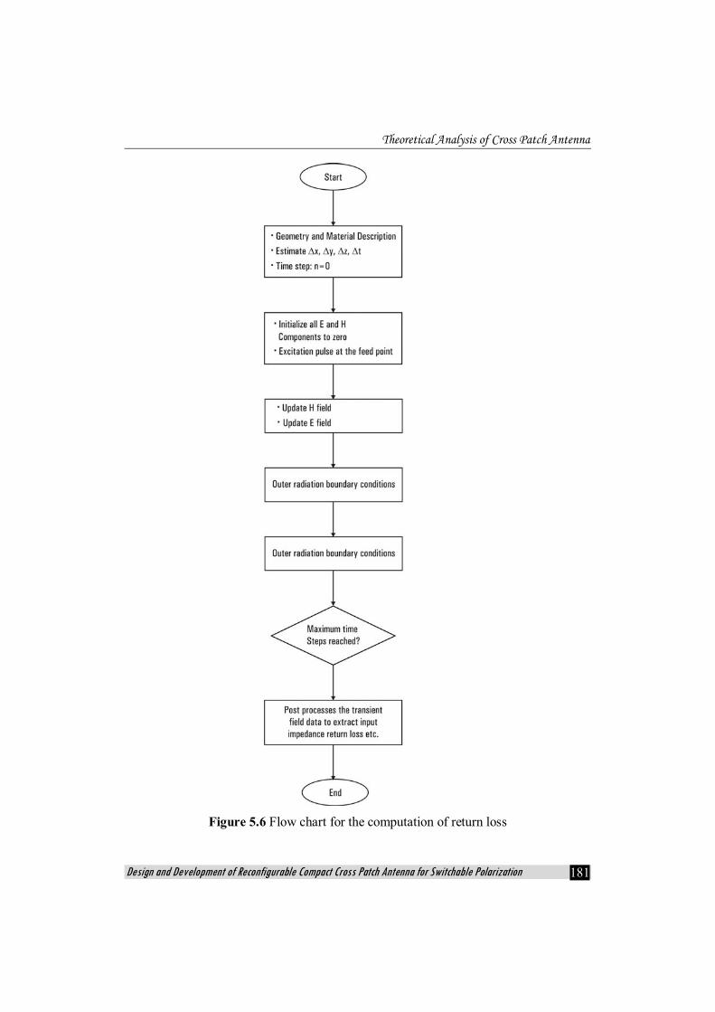
5.1.6 General flow chart of FDTD algorithm
The MATLAB based computer codes were developed to study the
resonant behavior of the proximity coupled printed cross patch antenna, cross
patch antenna with X-slot and frequency reconfigurable polarization diversity

Chapter-5
Department of Electronics, CUSAT 180
cross patch antenna. The general flow chart for the program to calculate the
return loss characteristics is shown in figure 5.6.
5.1.7 Return loss calculation
The voltage at the input port location is computed from the Ez field
components at the feed point over the entire simulation time interval. The
current at the feed point is calculated from the H field values around the feed
point using Ampere’s circuital law. The input impedance of the antenna is
computed as
( ) ( )( ) )10...(..................................................
,,
1 PIFFTPVFFTZ n
n
in −=ω
Where P is the suitable Zero padding used for taking FFT, zEV nz
n ∆= *
and In-1 is the current through the source.
Since microstrip line is modeled using Leubber’s staircase approach, the
internal impedance of source resistance Rs is taken as the characteristic
impedance (Z0) of microstrip line.
Reflection coefficient is given as ( ) 0 .......................(11)0
Z ZinZ Zin
ω−
Γ =+
Return loss in dB, ( )20log ...............................................(12)11 10S ω= Γ
The return loss computed in the above process is processed for
extracting the fundamental resonant frequency and 2:1 VSWR bandwidth
corresponding to the -10 dB return loss.
Theoretical Analysis of Cross Patch Antenna
Design and Development of Reconfigurable Compact Cross Patch Antenna for Switchable Polarization 181
Figure 5.6 Flow chart for the computation of return loss
Chapter-5
Department of Electronics, CUSAT 182
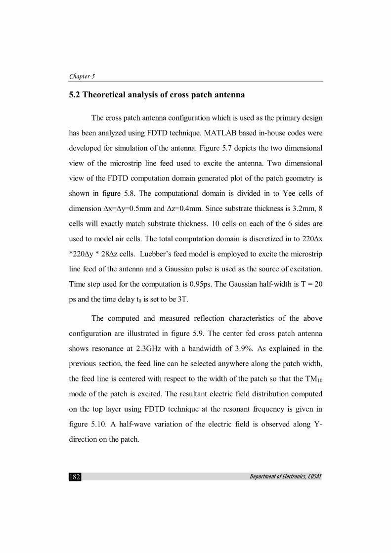
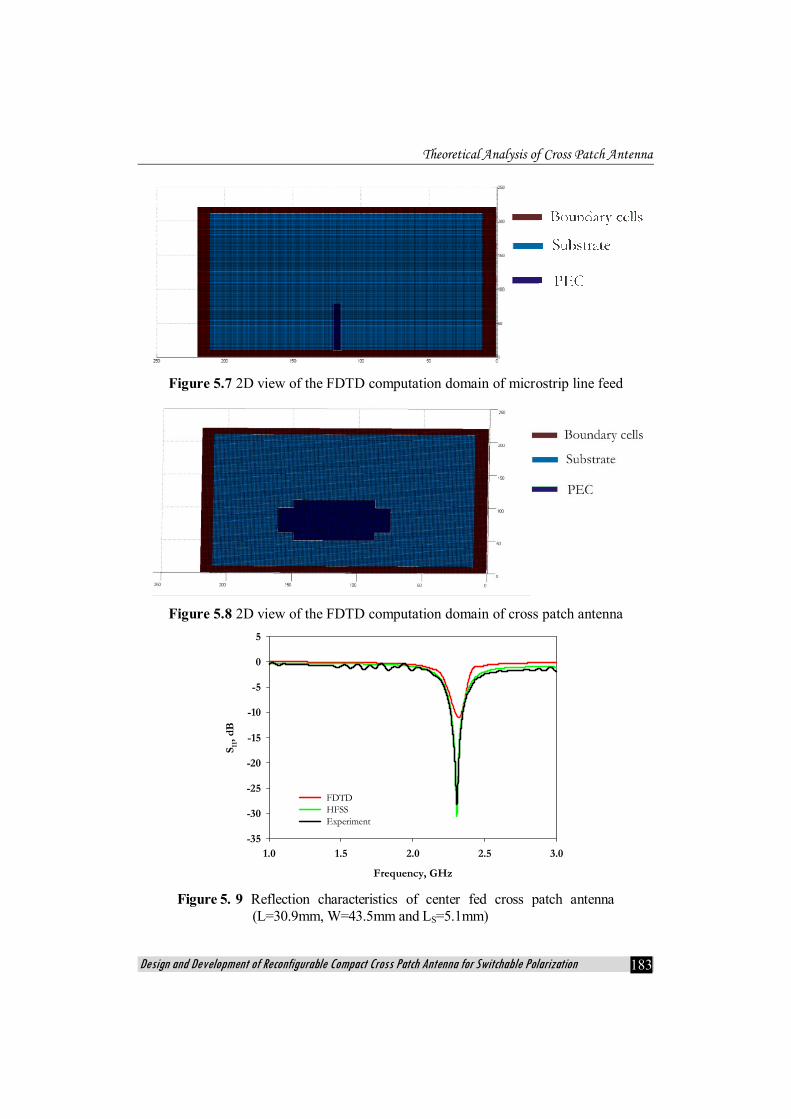
5.2 Theoretical analysis of cross patch antenna
The cross patch antenna configuration which is used as the primary design
has been analyzed using FDTD technique. MATLAB based in-house codes were
developed for simulation of the antenna. Figure 5.7 depicts the two dimensional
view of the microstrip line feed used to excite the antenna. Two dimensional
view of the FDTD computation domain generated plot of the patch geometry is
shown in figure 5.8. The computational domain is divided in to Yee cells of
dimension ∆x=∆y=0.5mm and ∆z=0.4mm. Since substrate thickness is 3.2mm, 8
cells will exactly match substrate thickness. 10 cells on each of the 6 sides are
used to model air cells. The total computation domain is discretized in to 220∆x
*220∆y * 28∆z cells. Luebber’s feed model is employed to excite the microstrip
line feed of the antenna and a Gaussian pulse is used as the source of excitation.
Time step used for the computation is 0.95ps. The Gaussian half-width is T = 20
ps and the time delay t0 is set to be 3T.
The computed and measured reflection characteristics of the above
configuration are illustrated in figure 5.9. The center fed cross patch antenna
shows resonance at 2.3GHz with a bandwidth of 3.9%. As explained in the
previous section, the feed line can be selected anywhere along the patch width,
the feed line is centered with respect to the width of the patch so that the TM10
mode of the patch is excited. The resultant electric field distribution computed
on the top layer using FDTD technique at the resonant frequency is given in
figure 5.10. A half-wave variation of the electric field is observed along Y-
direction on the patch.
Theoretical Analysis of Cross Patch Antenna
Design and Development of Reconfigurable Compact Cross Patch Antenna for Switchable Polarization 183
Figure 5.7 2D view of the FDTD computation domain of microstrip line feed
Figure 5.8 2D view of the FDTD computation domain of cross patch antenna
Figure 5. 9 Reflection characteristics of center fed cross patch antenna
(L=30.9mm, W=43.5mm and LS=5.1mm)
Frequency, GHz
1.0 1.5 2.0 2.5 3.0
S 11, d
B
-35
-30
-25
-20
-15
-10
-5
0
5
FDTDHFSSExperiment
Chapter-5
Department of Electronics, CUSAT 184
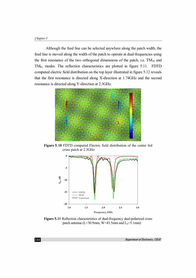
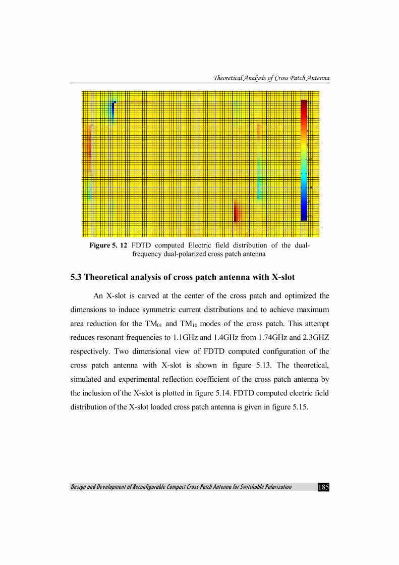
Although the feed line can be selected anywhere along the patch width, the feed line is moved along the width of the patch to operate at dual-frequencies using the first resonance of the two orthogonal dimensions of the patch, i.e. TM10 and TM01 modes. The reflection characteristics are plotted in figure 5.11. FDTD computed electric field distribution on the top layer illustrated in figure 5.12 reveals that the first resonance is directed along X-direction at 1.74GHz and the second resonance is directed along Y-direction at 2.3GHz.
Figure 5.10 FDTD computed Electric field distribution of the center fed
cross patch at 2.3GHz
Figure 5.11 Reflection characteristics of dual-frequency dual-polarized cross
patch antenna (L=30.9mm, W=43.5mm and LS=5.1mm)
Frequency, GHz
1.0 1.5 2.0 2.5 3.0
S 11, d
B
-20
-15
-10
-5
0
FDTDHFSSExperiment
Theoretical Analysis of Cross Patch Antenna
Design and Development of Reconfigurable Compact Cross Patch Antenna for Switchable Polarization 185
Figure 5. 12 FDTD computed Electric field distribution of the dual-
frequency dual-polarized cross patch antenna
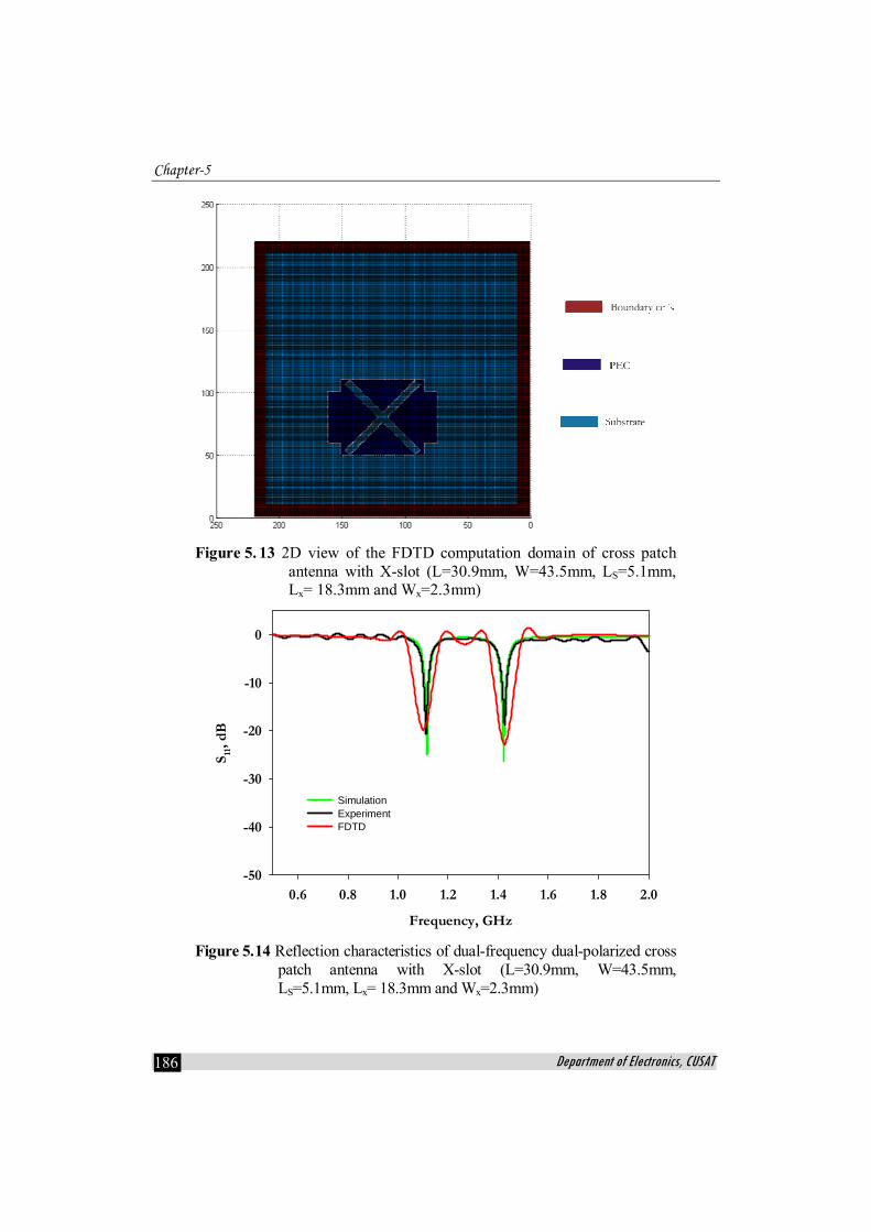
5.3 Theoretical analysis of cross patch antenna with X-slot
An X-slot is carved at the center of the cross patch and optimized the
dimensions to induce symmetric current distributions and to achieve maximum
area reduction for the TM01 and TM10 modes of the cross patch. This attempt
reduces resonant frequencies to 1.1GHz and 1.4GHz from 1.74GHz and 2.3GHZ
respectively. Two dimensional view of FDTD computed configuration of the
cross patch antenna with X-slot is shown in figure 5.13. The theoretical,
simulated and experimental reflection coefficient of the cross patch antenna by
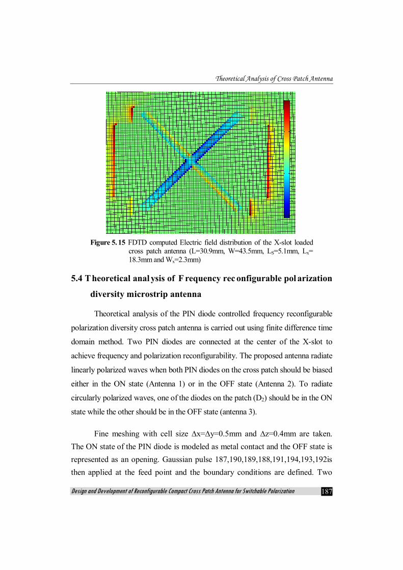
the inclusion of the X-slot is plotted in figure 5.14. FDTD computed electric field
distribution of the X-slot loaded cross patch antenna is given in figure 5.15.
Chapter-5
Department of Electronics, CUSAT 186
Figure 5. 13 2D view of the FDTD computation domain of cross patch
antenna with X-slot (L=30.9mm, W=43.5mm, LS=5.1mm, Lx= 18.3mm and Wx=2.3mm)
Figure 5.14 Reflection characteristics of dual-frequency dual-polarized cross
patch antenna with X-slot (L=30.9mm, W=43.5mm, LS=5.1mm, Lx= 18.3mm and Wx=2.3mm)
Frequency, GHz
0.6 0.8 1.0 1.2 1.4 1.6 1.8 2.0
S 11, d
B
-50
-40
-30
-20
-10
0
SimulationExperimentFDTD
Theoretical Analysis of Cross Patch Antenna
Design and Development of Reconfigurable Compact Cross Patch Antenna for Switchable Polarization 187
Figure 5. 15 FDTD computed Electric field distribution of the X-slot loaded
cross patch antenna (L=30.9mm, W=43.5mm, LS=5.1mm, Lx= 18.3mm and Wx=2.3mm)
5.4 Theoretical anal ysis of F requency rec onfigurable pol arization
diversity microstrip antenna
Theoretical analysis of the PIN diode controlled frequency reconfigurable
polarization diversity cross patch antenna is carried out using finite difference time
domain method. Two PIN diodes are connected at the center of the X-slot to
achieve frequency and polarization reconfigurability. The proposed antenna radiate
linearly polarized waves when both PIN diodes on the cross patch should be biased
either in the ON state (Antenna 1) or in the OFF state (Antenna 2). To radiate
circularly polarized waves, one of the diodes on the patch (D2) should be in the ON
state while the other should be in the OFF state (antenna 3).
Fine meshing with cell size ∆x=∆y=0.5mm and ∆z=0.4mm are taken. The ON state of the PIN diode is modeled as metal contact and the OFF state is represented as an opening. Gaussian pulse 187,190,189,188,191,194,193,192is then applied at the feed point and the boundary conditions are defined. Two

Chapter-5
Department of Electronics, CUSAT 188
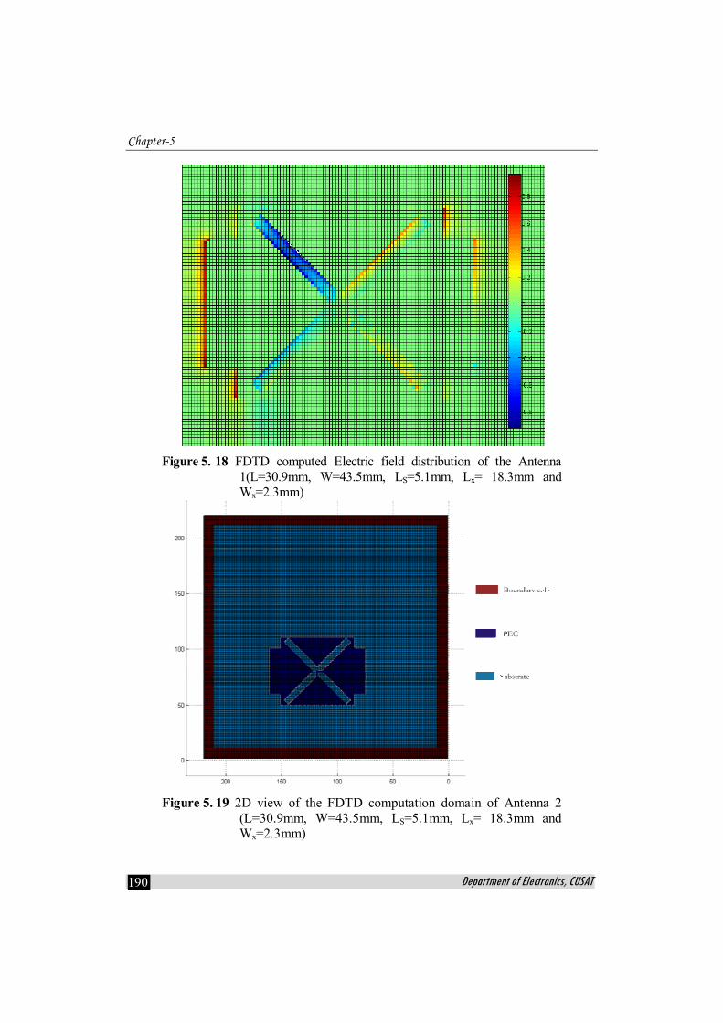
dimensional view of FDTD computed configuration of the Antenna 1 is shown in figure 5.16. A comparison between the theoretical, simulated and experimental reflection coefficient of the Antenna 1 is plotted in figure 5.17. FDTD computed electric field distribution of the Antenna 1 is given in figure 5.18.
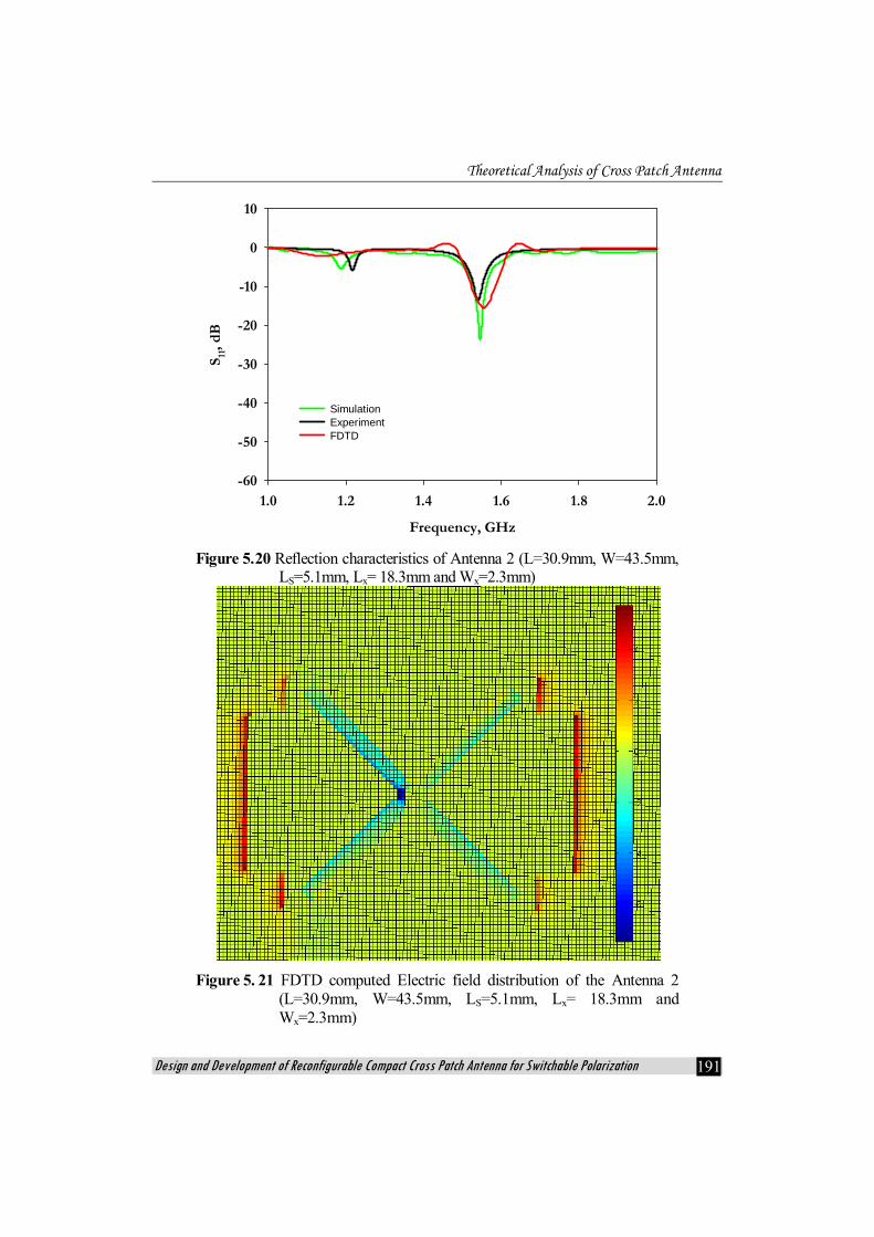
Two dimensional view of FDTD computed configuration of the Antenna 2 is shown in figure 5.19. A comparison between the theoretical, simulated and experimental reflection coefficient of the Antenna 2 is plotted in figure 5.20. FDTD computed surface cur electric field rent distribution of the Antenna 2 is given in figure 5.21.
Two dimensional view of FDTD computed configuration of the Antenna 3 is shown in figure 5.22. A comparison between the theoretical, simulated and experimental reflection coefficient of the Antenna 3 is plotted in figure 5.23. FDTD computed electric field distribution of the Antenna 3 is given in figure 5.24. Comparison of the measured, simulated and FDTD computed results of the three different antennas are summarized in Table 5.1.
Table 5.1 Comparison between Measured, Simulated and FDTD computed resonant frequency of Frequency reconfigurable polarization diversity microstrip antenna
Antenna Resonant Frequency, GHz
Experiment HFSS FDTD 1 1.474 1.475 1.484
2 1.54 1.54 1.55
3 1.45-1.536 1.45-1.53 1.44-1.53

Theoretical Analysis of Cross Patch Antenna
Design and Development of Reconfigurable Compact Cross Patch Antenna for Switchable Polarization 189
Figure 5. 16 2D view of the FDTD computation domain of Antenna
1(L=30.9mm, W=43.5mm, LS=5.1mm, Lx= 18.3mm and Wx=2.3mm)
Figure 5. 17 Reflection characteristics of Antenna 1 (L=30.9mm,
W=43.5mm, LS=5.1mm, Lx= 18.3mm and Wx=2.3mm)
Frequency, GHz
1.0 1.2 1.4 1.6 1.8 2.0 2.2 2.4
S 11, d
B
-50
-40
-30
-20
-10
0
10
ExperimentSimulationFDTD
Chapter-5
Department of Electronics, CUSAT 190
Figure 5. 18 FDTD computed Electric field distribution of the Antenna
1(L=30.9mm, W=43.5mm, LS=5.1mm, Lx= 18.3mm and Wx=2.3mm)
Figure 5. 19 2D view of the FDTD computation domain of Antenna 2
(L=30.9mm, W=43.5mm, LS=5.1mm, Lx= 18.3mm and Wx=2.3mm)
Theoretical Analysis of Cross Patch Antenna
Design and Development of Reconfigurable Compact Cross Patch Antenna for Switchable Polarization 191
Figure 5.20 Reflection characteristics of Antenna 2 (L=30.9mm, W=43.5mm,
LS=5.1mm, Lx= 18.3mm and Wx=2.3mm)
Figure 5. 21 FDTD computed Electric field distribution of the Antenna 2
(L=30.9mm, W=43.5mm, LS=5.1mm, Lx= 18.3mm and Wx=2.3mm)
Frequency, GHz
1.0 1.2 1.4 1.6 1.8 2.0
S 11, d
B
-60
-50
-40
-30
-20
-10
0
10
SimulationExperimentFDTD

Chapter-5
Department of Electronics, CUSAT 192
Figure 5. 22 2D view of the FDTD computation domain of Antenna 3
(L=30.9mm, W=43.5mm, LS=5.1mm, Lx= 18.3mm and Wx=2.3mm)
Figure 5. 23 Reflection characteristics of Antenna 3 (L=30.9mm,
W=43.5mm, LS=5.1mm, Lx= 18.3mm and Wx=2.3mm)
Frequency, GHz
1.0 1.2 1.4 1.6 1.8 2.0
S 11, d
B
-50
-40
-30
-20
-10
0
10
SimulationExperimentFDTD

Theoretical Analysis of Cross Patch Antenna
Design and Development of Reconfigurable Compact Cross Patch Antenna for Switchable Polarization 193
Figure 5. 24 FDTD computed Electric field distribution of the Antenna 3 (L=30.9mm, W=43.5mm, LS=5.1mm, Lx= 18.3mm and Wx=2.3mm)
5.5 Chapter Summary
FDTD based numerical computation is used to analyze the performance
of cross patch antenna with and without X-slot. PIN diode controlled frequency
and polarization reconfigurable compact cross patch antenna is also analyzed
using FDTD. The staircase approximation is employed to derive the slant edges
of the X-slot. MATLAB based in-house codes were developed for simulation of
the antenna. Luebber’s feed model is employed to excite the microstrip line
feed of the antenna and a Gaussian pulse is used as the source of excitation.
Time step used for the computation is 0.95ps. The Gaussian half-width is T =
20 ps and the time delay t0 is set to be 3T. Various steps involved in the
extraction of antenna parameters along with the assumptions taken in the
implementation of the algorithm are also described. The predicted results are
experimentally verified by fabricating and testing different printed cross patch
antennas.

Chapter-5
Department of Electronics, CUSAT 194
References
1 K. S. Yee, Numerical solution of initial boundary value problems
involving Maxwell’s equations in isotropic media, IEEE Transactions on
Antennas and Propagation, Vol.14, No. 3, pp. 302-307, 1966.
2 X. Zhang and K. K. Mei, Time domain finite difference approach to the
calculation of the frequency dependent characteristics of microstrip
discontinuities, IEEE Trans. Microwave Theory Tech., Vol. 36, pp.
1775-1787, Dec. 1988.
3 Hallond, R, and J. W. Williams, Total field versus scattered field finite
difference codes: A comparative Assessment, IEEE Transactions on
Nuclear Science, Vol. 30, No.6, pp. 4583-4588, 1983.
4 Enquist and Majada, Absorbing Boundary Conditions for the Numerical
simulation of waves, Mathematics of Computation, Vol. 31, pp. 629-651,
1977.
5 Mur G, Absorbing boundary conditions for the Finite Difference
Approximation of the Time domain Electromagnetic field equations, IEEE
Trans. Electromagn. Compat., Vol .EMC-23, pp. 377-382, Nov. 1981
6 V. Jandhyala, E. Michielssen, and R. Mittra, FDTD signal extrapolation
using the forward-backward autoregressive model, IEEE Microwave
and Guide Wave Letters, Vol. 4, pp. 163-165, June 1994.
7 R.J Leubbers and H.S Langdon., A simple feed Model that reduces Time
steps Needed for FDTD Antenna and Microstrip Calculations, IEEE
Trans. Antennas and Propogat., Vol.44,No.7, pp.1000-1005, July 1996.

Theoretical Analysis of Cross Patch Antenna
Design and Development of Reconfigurable Compact Cross Patch Antenna for Switchable Polarization 195
8 R.J Leubbers,Karl s Kunz,Micheal Schneider and Forrest Hunsberger.,
A finite difference time Domain near zone to far zone transformation,
IEEE Trans. Antennas and Propagat., Vol.39,pp429-433,April 1991.
9 Martin L Zimmerman and Richard Q Lee, Use of FDTD method in the
design of microstrip antenna arrays, Int.Journal of Microwave and
Millimeter wave Comp. aided Engg., Vol.4, No.1,pp 58-66,1994.


![[FDM][FEM][FEM][FVM] Mattiussi - The Finite Volume, Finite Difference, And Finite Elements Methods As Numerical Methods For Physical Field Problems - Fdtd(5)](https://img.pdfslide.us/doc/110x75/557207b9497959fc0b8bb656/fdmfemfemfvm-mattiussi-the-finite-volume-finite-difference-and-finite-elements-methods-as-numerical-methods-for-physical-field-problems-fdtd5.jpg)


![arXiv:1301.4539v1 [cs.DC] 19 Jan 2013 · FDTD, multicore, cache reuse, ... At CEA, the French Nuclear Agency, we develop yet an-other FDTD (Finite Difference in Time Domain) code,](https://img.pdfslide.us/doc/110x75/5b7f43887f8b9aca778bdab3/arxiv13014539v1-csdc-19-jan-2013-fdtd-multicore-cache-reuse-at-cea.jpg)


![Computational Environment for Simulating Lightning Strokes in a Power Substation … · 2012-11-02 · finite-difference time-domain method (FDTD) [1,2] and the finite element method](https://img.pdfslide.us/doc/110x75/5e67c35014d9c9284352a2fa/computational-environment-for-simulating-lightning-strokes-in-a-power-substation.jpg)