Embed Size (px)
Citation preview
Co
mm
un
iCati
on
© 2016 WILEY-VCH Verlag GmbH & Co. KGaA, Weinheimwileyonlinelibrary.com1603885 (1 of 9)
50-Fold EQE Improvement up to 6.27% of Solution-Processed All-Inorganic Perovskite CsPbBr3 QLEDs via Surface Ligand Density Control
Jianhai Li, Leimeng Xu, Tao Wang, Jizhong Song,* Jiawei Chen, Jie Xue, Yuhui Dong, Bo Cai, Qingsong Shan, Boning Han, and Haibo Zeng*
J. Li, L. Xu, T. Wang, Prof. J. Song, J. Chen, J. Xue, Y. Dong, B. Cai, Q. Shan, B. Han, Prof. H. ZengInstitute of Optoelectronics and NanomaterialsHerbert Gleiter Institute of NanoscienceMIIT Key Laboratory of Advanced Display Materials and DevicesSchool of Materials Science and EngineeringNanjing University of Science and TechnologyNanjing 210094, ChinaE-mail: [email protected]; [email protected]
DOI: 10.1002/adma.201603885
purification process, especially for a simple reprecipitation technique. Recently, Huang et al. introduced an emulsion system to tackle this problem for CH3NH3PbBr3 QDs from a different perspective by using two immiscible solvents,[22] but it is still difficult to find a simple reprecipitation technique by using suitable solvents and further optimize the device perfor-mance. In additon, no research has been done systematically on electric properties of perovskite-based light-emitting devices under handy surface purification. For an ideal QLED, high ink stability, high PL QYs, and high charge injection efficiency are all necessary. However, how to synchronously obtain these indispensable factors has still been a huge challenge for high-performance CsPbX3 QLED devices.
Here, we demonstrate a highly efficient solution-processed CsPbBr3 QLED through balancing surface passivation and car-rier injection via ligand density control. A recyclable treatment on QDs using hexane/ethyl acetate mixed solvent is proposed to control the surface ligand density for the first time after investigating a series of solvents. We perform detailed studies of the effects of the aforementioned purification process on CsPbBr3 QDs, assembled films, and final devices using various characterization methods. Interestingly, ink stability, PL QYs, film uniformity, and microstructure can all be preserved at high levels after proper treating. Meantime, EQE of 6.27% was obtained for CsPbX3 LEDs, and it has been 50-fold enhanced when compared with QDs using one cycle of acetone treat-ment. Correspondingly, the current efficiency was also 30-fold improved from 0.43 cd A−1 to 13.3 cd A−1, which verified the effective charge injection due to ligand density control. The remarkable efficiency for CsPbBr3 QLED represents a major improvement for inorganic-perovskite LEDs (IPLEDs) and reveals a direction, which receives insufficient attention, to meliorate IPLED devices by moderate surface treatment.
Compared to surface ligand exchange,[23,24] the control of ligand density on QD surfaces is a more proper strategy to pro-mote the performance of CsPbX3 QLEDs, which has not been deeply studied. To synchronously keep ink stability, PL QY, and carrier injection at high levels, a recyclable treatment on QDs using hexane/ethyl acetate mixed solvent was applied to control the surface ligand density as shown in Figure 1 and Figure S1 in the Supporting Information. Excessive ligands lead to the assembled films with poor carrier injection and transporta-tion, but insufficient ligands cause the QDs to have the low PL QYs and poor ink stabilities. Only a suitable density of sur-face ligands can provide the QDs with optimal optoelectronic properties. Among a large number of tried solvents (Table S1,
The external quantum efficiency (EQE) of the organic–inorganic hybrid CH3NH3PbBr3 (MAPbBr3) perovskite light-emitting diodes (LEDs) has been drastically improved up to 8.53%[1] from the first reported 0.76%[2] within only 1 year.[3–5] Comparatively, all-inorganic CsPbX3 (X = Cl, Br, I) perovskites have higher stability,[6–8] evidenced by the room-temperature lasing in ambient atmosphere without inert gas protection.[9] Moreover, such inorganic perovskites are of higher photo-luminescence (PL) quantum yields (QYs),[10–12] demonstrated by more than 90% QY for green PL from CsPbBr3 quantum dots (QDs).[13,14] Therefore, the all-inorganic perovskite quantum-dot light-emitting diodes (QLEDs) could be developed to have high performances, including high electroluminescence (EL) efficiency and brightness. However, in contrast to the tenfold EQE improvement of MAPbBr3 LEDs, CsPbX3 LEDs are still hovering at a lower level, although CsPbX3 QDs have higher PL QYs and stability. For examples, the EQE of the first reported CsPbBr3 LED from Zeng group is only of 0.12%.[15] Recently, Zhang et al. reported an EQE of 0.06% through the interface engineering.[16] Li et al. achieved an EQE of 0.19% by using trimethylaluminum to crosslink nanocrystals in the devices.[17]
Aside from the optimizations of device structure, the surface state of QDs is another crucial factor for the performances of a QLED. Actually, the surface ligands have double side effect on QLEDs. On the one hand, a large number of ligands are needed to provide sufficient surface passivation, which can get rid of surface defects, inducing high PL QYs and ink stability.[18,19] On the other hand, excessive ligands will form an insulating layer because oleylamine and oleic acid organics used in the synthesis of CsPbX3 QDs all have very poor electric conduc-tivity, and then block charge injection inside the QLED.[20,21] Compared to the classical chalcogenide QDs, perovskites are more ionic in nature and sensitive to many polar solvents, resulting in a great quantity of difficulties for a suitable QD
www.advmat.de
Adv. Mater. 2017, 29, 1603885
www.advancedsciencenews.com
Co
mm
un
iCatio
n
© 2016 WILEY-VCH Verlag GmbH & Co. KGaA, Weinheim wileyonlinelibrary.com (2 of 9) 1603885
Supporting Information), the mixture of hexane/ethyl acetate was found to have an outstanding ability to control the ligand density on QD surfaces, which can be explained by the relation-ship between the polarity of solvents and the ionicity of perovs-kites (Table S2, Supporting Information), which will result in more ionic and dynamic interactions.[25,26]
Such control of ligand density can be well confirmed by nuclear magnetic resonance (NMR), X-ray photoelectron spectroscopy (XPS), and Fourier transform infrared (FTIR) spectroscopy characterizations (Figure 1b–e). The surface ligands were first analyzed by NMR spectra as shown in Figure 1b,c. The total concentration of the oleyl species (deter-mined from resonance 5) is gradually reduced as the treating
cycle increases. One cycle is insufficient, revealed by the charac-teristic resonances of a terminal alkene, presumable octadecene (ODE), which was a side product for colloidal synthesis, at 4.94 and 5.8 ppm (the reference spectra of ODE, oleic acid, and oleylamine are shown in Figure S2 in the Supporting Informa-tion). These side products and excessive surface ligands act as an “insulation layer” between adjacent particles in subsequent assembled QD thin films, which will degrade the electrical properties and the carrier transporting capabilities. The ligand density (defined as the concentration of oleyl species around the nanocrystal) is used to quantitatively evaluate the con-tent of ligands obtained by the combination of the transmis-sion electron microscopy (TEM) and NMR results (Figure S3,
www.advmat.de
Adv. Mater. 2017, 29, 1603885
www.advancedsciencenews.com
Figure 1. Surface ligand density control (SLDC). a) Schematic illustration of the control of ligand density on CsPbBr3 QD surfaces and the corre-sponding changes of ink stability, PL QY, and carrier injection. b,c) 1H NMR full spectrum (b) and enlarged spectrum (c) of CsPbBr3 QDs with different cycles of hexane/ethyl acetate treatment, indicating the gradual decrease of ODE, oleylamine, and oleic acid groups. d) Relative content of carbon and nitrogen (from ligands) to Cs in CsPbBr3 QDs with different treating cycles plotted from XPS data. e) FTIR surface imaging of CC stretching mode at 2923 cm−1 of CsPbBr3 QD films with different cycles of treatment obtained by FTIR microspectroscopy.
Co
mm
un
iCati
on
© 2016 WILEY-VCH Verlag GmbH & Co. KGaA, Weinheimwileyonlinelibrary.com1603885 (3 of 9)
Supporting Information). The ligand density treated with one, two, and three cycles is about 6.7, 4.8, and 3.9 nm−2, respec-tively, indicating a gradually reduced content of ligands on QD surfaces, which is favorable for the subsequent charge injection in QLED devices.
Furthermore, the gradual reduction of surface ligand was further verified by the decrease of relative peak intensity ratios of C/Cs, C/Pb, C/Br, N/Cs, N/Pb, and N/Br from XPS measure-ments as shown in Figure 1d and Figure S4 and S5 in the Sup-porting Information. The surface ligand changes on QD thin film were also checked by FTIR analysis as shown in Figure S6 (Supporting Information). The FT-IR peaks located at 2923 and 2854 cm−1 are ascribed to CC and CH stretching modes of the CH2 group, which exhibited an obvious decrease with increased treating cycles. Moreover, the FTIR mapping result (Figure 1e and Figure S7, Supporting Information), obtained through scanning CC stretching mode, demonstrated that the organic molecules could be removed after three cycles of purification, which can be further confirmed by the thermo-gravimetric analysis (TGA) curves (Figure S8, Supporting Information). In addition, X-ray diffraction (XRD) patterns (Figure S9a, Supporting Information) revealed that the CsPbBr3 QDs maintained cubic phase after three cycles purifying. Such a purification process is expected to balance ink stability, PL QYs, and charge injection.
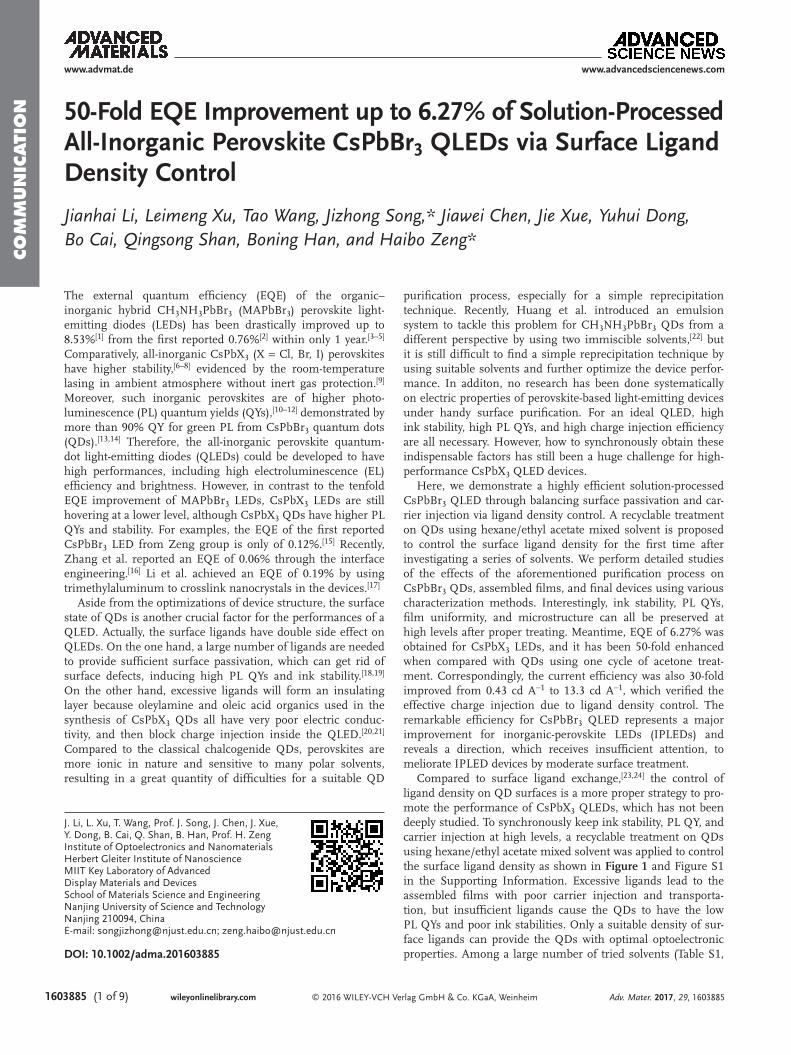
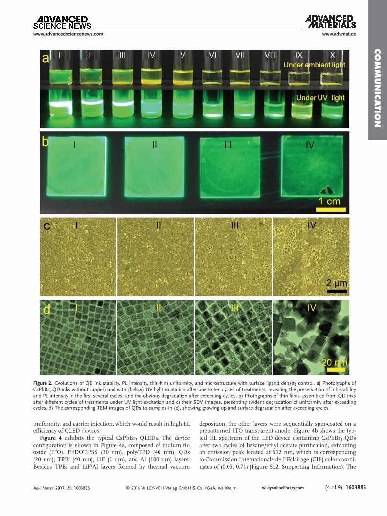
Figure 2 presents the evolution of QD ink stability, PL inten-sity, thin-film uniformity, and microstructure with the above purification process. Figure 2a shows photographs of CsPbBr3 QD inks without (upper) and with (below) UV light excitation after one to ten cycles of treatments. Excessive purifying cycles (>3 cycles) result in the obvious aggregation and precipitate due to the serious loss of surface ligands. Moreover, the PL under UV light excitation also weakens due to the increase of surface defects with the loss of surface ligands, which is confirmed by the PL evolution of QD thin films as shown in Figure 2b.
The solution-processed assemble of QD thin film is essen-tial for the integration of QLED devices, and the thin-film quality is crucial for the final performances. From the evolu-tion of thin films reflected by Figure 2b,c, it can be found that the uniformity of spin-coated thin films can be preserved very well in the first three cycles, and then destroyed very seriously after four cycles due to the poor ink stability. Such thin-film uniformity changes will greatly affect the charge transport within QLED devices. When QDs were purified for four cycles, some pinholes emerge in the films (Figure S10, Supporting Information), which even induces the short circuit confirmed in Figure S11 in the Supporting Information. The TEM images were used to further study the effects of purifying cycles on the microstructure of QDs as shown in Figure 2d. The QD size has only a slight increase from 8.1 to 9.2 nm within the first three cycles, while huge increase up to 20 nm was observed after four cycles of treatment due to the serious loss of surface ligands as confirmed by Figure 1. The growth of crystal is attributed to the strong ionic feature of CsPbX3 perovskites, which induces the fast growth under insufficient surface ligands. Further-more, it is obvious that the surface of QDs has been seriously destroyed, and becomes very irregular, inducing the creation of a large number of surface defects. Above degradations of ink stability (Figure 2a), PL (Figure 2a,b), and thin-film uniformity
(Figure 2b,c) can be attributed to the growth up and surface degradation (Figure 2d) observed here.
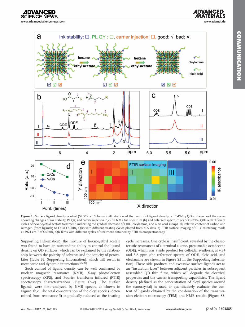
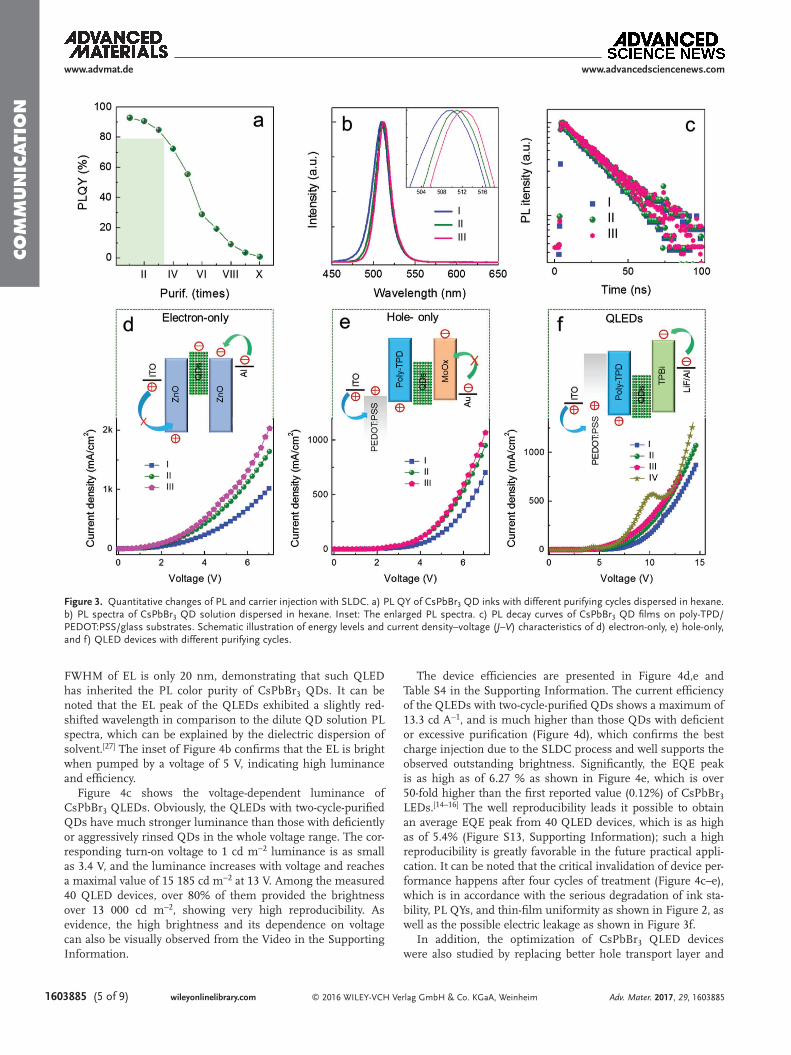
The quantitative changes of PL and carrier injection with surface ligand density control (SLDC) are shown in Figure 3. Fortunately, PL QYs higher than 80% can be still preserved within the first three cycles of purification as shown in Figure 3a. Especially, the PL QYs are slightly reduced from 92% to 90% after two cycles of purification, which completely meets the requirement of high performance QLEDs. The PL peaks just slightly redshift from 510 to 512 nm after three cycles of purification (Figure 3b), corresponding with the UV–vis absorption spectra shown in Figure S9b in the Sup-porting Information. It likely arises from the slight growth of the QDs from 8.1 to 9.2 nm as presented in Figure 2d. The full width at half maximum (FWHM) of PL peak become nar-rower from 22 to 19 nm (Figure 3b), maintaining very high color purity. The PL decay curves of QDs purified for the first three cycles are shown in Figure 3c, which can be fitted well with the bi-exponential function (Table S3, Supporting Infor-mation). The short radiative lifetimes suggest that the PL of CsPbBr3 QDs derives from excitonic recombination, which can be explained by both higher exciton binding energy for bulk CsPbBr3 (35–40 meV) and quantum confinement in QDs.[10] Correspondingly, the average PL lifetimes are slightly increased from 5.4 (I) to 7.6 (II), and further to 6.9 ns (III) (Figure 3c and Table S3, Supporting Information), indicating no much change on luminescence properties and defective trappers of QDs. Aggressive treating cycles resulted in the obvious growth up of QDs and surface degradation, which will weaken PL QYs and ink stability as shown in Figure 2a, exhibiting notorious device performances (Figure S14, Sup-porting Information).
Figure 3d–f demonstrates the effect of the SLDC process on the charge injection into CsPbBr3 QD thin films. For the electron-only device, the currents obviously increase in the first three treating cycles, demonstrating the increased elec-tron injection efficiency (Figure 3d). Similar improvement of the hole injection efficiency can be observed from the hole-only device as shown in Figure 3e. Such improved charge injection was also confirmed by the full QLED. Figure 3f shows that the corresponding current densities of the QLED devices have been substantially improved, for instance, 16, 50, and 87 mA cm−2 at 7 V for QLEDs with QDs purified for one, two, and three cycles, respectively. These results indicated that the charge injection and transport capabilities of CsPbBr3 QD films can be indeed boosted after appropriate surface purification. However, as shown in Figure 3f, the obvious electric leakage appears after four or more cycles due to the degradation of QDs (Figure 2d) and assembled thin films (Figure 2c).
It is noteworthy to point out that the preservation of high PL QYs and the improvement of charge injection can be simul-taneously achieved after two cycles of hexane/ethyl acetate purification on CsPbBr3 QDs, which are usually contradictory during the indispensable QD purification process,[18,19] forming a critical weakness for QLEDs.[20,21] Therefore, above charac-terizations on such a purification process (Figure 1) and the resultant evolutions (Figure 2 and 3) revealed that the balance between surface passivation and carrier injection can lead to the coexistence of high levels of ink stability, PL QYs, thin-film
www.advmat.de
Adv. Mater. 2017, 29, 1603885
www.advancedsciencenews.com
Co
mm
un
iCatio
n
© 2016 WILEY-VCH Verlag GmbH & Co. KGaA, Weinheim wileyonlinelibrary.com (4 of 9) 1603885
uniformity, and carrier injection, which would result in high EL efficiency of QLED devices.
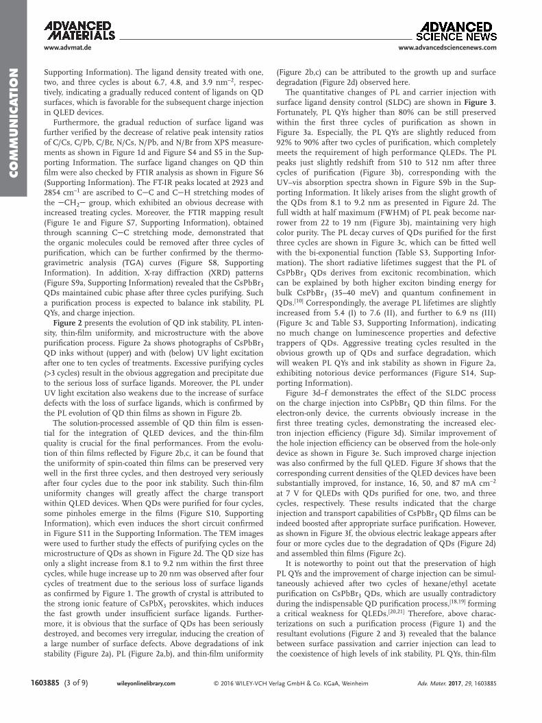
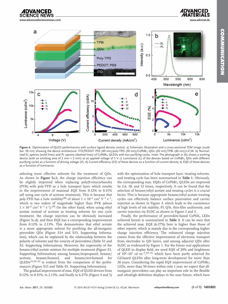
Figure 4 exhibits the typical CsPbBr3 QLEDs. The device configuration is shown in Figure 4a, composed of indium tin oxide (ITO), PEDOT:PSS (30 nm), poly-TPD (40 nm), QDs (20 nm), TPBi (40 nm), LiF (1 nm), and Al (100 nm) layers. Besides TPBi and LiF/Al layers formed by thermal vacuum
deposition, the other layers were sequentially spin-coated on a prepatterned ITO transparent anode. Figure 4b shows the typ-ical EL spectrum of the LED device containing CsPbBr3 QDs after two cycles of hexane/ethyl acetate purification, exhibiting an emission peak located at 512 nm, which is corresponding to Commission Internationale de L’Eclairage (CIE) color coordi-nates of (0.05, 0.71) (Figure S12, Supporting Information). The
www.advmat.de
Adv. Mater. 2017, 29, 1603885
www.advancedsciencenews.com
Figure 2. Evolutions of QD ink stability, PL intensity, thin-film uniformity, and microstructure with surface ligand density control. a) Photographs of CsPbBr3 QD inks without (upper) and with (below) UV light excitation after one to ten cycles of treatments, revealing the preservation of ink stability and PL intensity in the first several cycles, and the obvious degradation after exceeding cycles. b) Photographs of thin films assembled from QD inks after different cycles of treatments under UV light excitation and c) their SEM images, presenting evident degradation of uniformity after exceeding cycles. d) The corresponding TEM images of QDs to samples in (c), showing growing up and surface degradation after exceeding cycles.
Co
mm
un
iCati
on
© 2016 WILEY-VCH Verlag GmbH & Co. KGaA, Weinheimwileyonlinelibrary.com1603885 (5 of 9)
FWHM of EL is only 20 nm, demonstrating that such QLED has inherited the PL color purity of CsPbBr3 QDs. It can be noted that the EL peak of the QLEDs exhibited a slightly red-shifted wavelength in comparison to the dilute QD solution PL spectra, which can be explained by the dielectric dispersion of solvent.[27] The inset of Figure 4b confirms that the EL is bright when pumped by a voltage of 5 V, indicating high luminance and efficiency.
Figure 4c shows the voltage-dependent luminance of CsPbBr3 QLEDs. Obviously, the QLEDs with two-cycle-purified QDs have much stronger luminance than those with deficiently or aggressively rinsed QDs in the whole voltage range. The cor-responding turn-on voltage to 1 cd m−2 luminance is as small as 3.4 V, and the luminance increases with voltage and reaches a maximal value of 15 185 cd m−2 at 13 V. Among the measured 40 QLED devices, over 80% of them provided the brightness over 13 000 cd m−2, showing very high reproducibility. As evidence, the high brightness and its dependence on voltage can also be visually observed from the Video in the Supporting Information.
The device efficiencies are presented in Figure 4d,e and Table S4 in the Supporting Information. The current efficiency of the QLEDs with two-cycle-purified QDs shows a maximum of 13.3 cd A−1, and is much higher than those QDs with deficient or excessive purification (Figure 4d), which confirms the best charge injection due to the SLDC process and well supports the observed outstanding brightness. Significantly, the EQE peak is as high as of 6.27 % as shown in Figure 4e, which is over 50-fold higher than the first reported value (0.12%) of CsPbBr3 LEDs.[14–16] The well reproducibility leads it possible to obtain an average EQE peak from 40 QLED devices, which is as high as of 5.4% (Figure S13, Supporting Information); such a high reproducibility is greatly favorable in the future practical appli-cation. It can be noted that the critical invalidation of device per-formance happens after four cycles of treatment (Figure 4c–e), which is in accordance with the serious degradation of ink sta-bility, PL QYs, and thin-film uniformity as shown in Figure 2, as well as the possible electric leakage as shown in Figure 3f.
In addition, the optimization of CsPbBr3 QLED devices were also studied by replacing better hole transport layer and
www.advmat.de
Adv. Mater. 2017, 29, 1603885
www.advancedsciencenews.com
Figure 3. Quantitative changes of PL and carrier injection with SLDC. a) PL QY of CsPbBr3 QD inks with different purifying cycles dispersed in hexane. b) PL spectra of CsPbBr3 QD solution dispersed in hexane. Inset: The enlarged PL spectra. c) PL decay curves of CsPbBr3 QD films on poly-TPD/PEDOT:PSS/glass substrates. Schematic illustration of energy levels and current density–voltage (J–V) characteristics of d) electron-only, e) hole-only, and f) QLED devices with different purifying cycles.
Co
mm
un
iCatio
n
© 2016 WILEY-VCH Verlag GmbH & Co. KGaA, Weinheim wileyonlinelibrary.com (6 of 9) 1603885
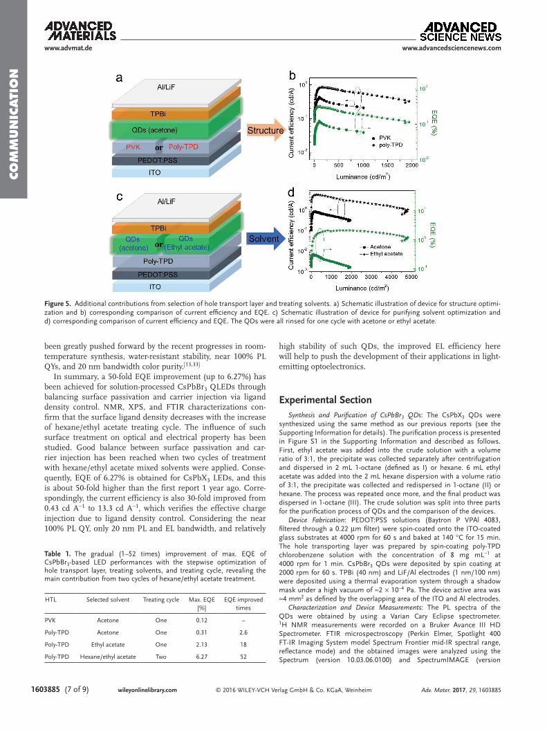
selecting more effective solvents for the treatment of QDs. As shown in Figure 5a,b, the charge injection efficiency can be slightly improved when replacing poly(9-vinycarbazole) (PVK) with poly-TPD as a hole transport layer, which results in the improvement of maximal EQE from 0.12% to 0.31% (all using one cycle of acetone treatment). This is because that poly-TPD has a hole mobility[28] of about 1 × 10⁻⁴ cm2 V−1 s−1, which is two orders of magnitude higher than PVK (about 1 × 10⁻⁶ cm2 V−1 s−1).[29] On the other hand, when using ethyl acetate instead of acetone as treating solvents for one cycle treatment, the charge injection can be obviously increased (Figure 5c,d), and then EQE has a corresponding improvement from 0.12% to 2.13%. This demonstrates that ethyl acetate is a more appropriate solvent for purifying the all-inorganic perovskite QDs (Figure S14 and S15, Supporting Informa-tion), which can be explained by the relationship between the polarity of solvents and the ionicity of perovskites (Table S1 and S2, Supporting Information). Moreover, the superiority of the hexane/ethyl acetate mixture for multiple treatment (Figure S1, Supporting Information) among hexane/isopropanol, hexane/acetone, hexane/butanol, and hexane/tert-butanol for QLEDs[14,30–32] is evident from the comparison of the perfor-mances (Figure S15 and Table S5, Supporting Information).
The gradual improvement of max. EQE of QLED devices from 0.12%, to 0.31%, to 2.13%, and finally to 6.27% (Figure 4 and 5)
with the optimization of hole transport layer, treating solvents, and treating cycle has been summarized in Table 1. Obviously, the corresponding max. EQEs of CsPbBr3 QLEDs are improved by 2.6, 18, and 52 times, respectively. It can be found that the selection of hexane/ethyl acetate and treating cycles is a crucial factor. This is because appropriate hexane/ethyl acetate treating cycles can effectively balance surface passivation and carrier injection as shown in Figure 3, which leads to the coexistence of high levels of ink stability, PL QYs, thin-film uniformity, and carrier injection via SLDC as shown in Figure 2 and 3.
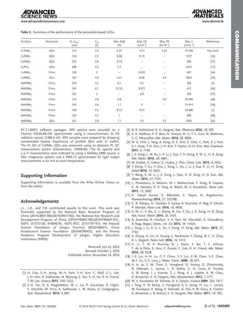
Finally, the performance of perovskite-based CsPbX3 LEDs achieved herein is summarized in Table 2. It can be seen that the achieved max. EQE (6.27%) here is higher than those of other reports, which is mainly due to the corresponding higher charge injection efficiency. The enhanced charge injection comes from the effective improvement of electronic transport from electrodes to QD layers, and among adjacent QDs after SLDC as evidenced by Figure 1. For the future real applications of QLED in display field, we need EQE of 20% and brightness of 102–103 cd m−2,[18–21] which have been partly achieved for Cd-based QLEDs after long-term development for more than 20 years. Considering the rapid EQE improvement of CsPbBr3 LEDs, more than 50 times within only 1 year, we expect that all-inorganic perovskites can play an important role in the flexible and ultrahigh definition displays in the near future, which have
www.advmat.de
Adv. Mater. 2017, 29, 1603885
www.advancedsciencenews.com
Figure 4. Optimization of QLED performances with surface ligand density control. a) Schematic illustration and a cross-sectional TEM image (scale bar: 50 nm) showing the device architecture: ITO/PEDOT: PSS (40 nm)/poly-TPD (30 nm)/CsPbBr3 QDs (20 nm)/TPBi (40 nm)/LiF/Al. b) Normal-ized EL spectra (solid lines) and PL spectra (dashed lines) of CsPbBr3 QLEDs with two purifying cycles. Inset: The photograph in (b) shows a working device (with an emitting area of 2 mm × 2 mm) at an applied voltage of 5 V. c) Luminance (L) of the devices based on CsPbBr3 QDs with different purifying cycles as a function of driving voltage (V). d) Current efficiency (CE) of these devices as a function of current density. e) EQE of these devices as a function of luminance.
Co
mm
un
iCati
on
© 2016 WILEY-VCH Verlag GmbH & Co. KGaA, Weinheimwileyonlinelibrary.com1603885 (7 of 9)
www.advmat.de
Adv. Mater. 2017, 29, 1603885
www.advancedsciencenews.com
been greatly pushed forward by the recent progresses in room-temperature synthesis, water-resistant stability, near 100% PL QYs, and 20 nm bandwidth color purity.[13,33]
In summary, a 50-fold EQE improvement (up to 6.27%) has been achieved for solution-processed CsPbBr3 QLEDs through balancing surface passivation and carrier injection via ligand density control. NMR, XPS, and FTIR characterizations con-firm that the surface ligand density decreases with the increase of hexane/ethyl acetate treating cycle. The influence of such surface treatment on optical and electrical property has been studied. Good balance between surface passivation and car-rier injection has been reached when two cycles of treatment with hexane/ethyl acetate mixed solvents were applied. Conse-quently, EQE of 6.27% is obtained for CsPbX3 LEDs, and this is about 50-fold higher than the first report 1 year ago. Corre-spondingly, the current efficiency is also 30-fold improved from 0.43 cd A−1 to 13.3 cd A−1, which verifies the effective charge injection due to ligand density control. Considering the near 100% PL QY, only 20 nm PL and EL bandwidth, and relatively
high stability of such QDs, the improved EL efficiency here will help to push the development of their applications in light-emitting optoelectronics.
Experimental SectionSynthesis and Purification of CsPbBr3 QDs: The CsPbX3 QDs were
synthesized using the same method as our previous reports (see the Supporting Information for details). The purification process is presented in Figure S1 in the Supporting Information and described as follows. First, ethyl acetate was added into the crude solution with a volume ratio of 3:1, the precipitate was collected separately after centrifugation and dispersed in 2 mL 1-octane (defined as I) or hexane. 6 mL ethyl acetate was added into the 2 mL hexane dispersion with a volume ratio of 3:1, the precipitate was collected and redispersed in 1-octane (II) or hexane. The process was repeated once more, and the final product was dispersed in 1-octane (III). The crude solution was split into three parts for the purification process of QDs and the comparison of the devices.
Device Fabrication: PEDOT:PSS solutions (Baytron P VPAl 4083, filtered through a 0.22 µm filter) were spin-coated onto the ITO-coated glass substrates at 4000 rpm for 60 s and baked at 140 °C for 15 min. The hole transporting layer was prepared by spin-coating poly-TPD chlorobenzene solution with the concentration of 8 mg mL−1 at 4000 rpm for 1 min. CsPbBr3 QDs were deposited by spin coating at 2000 rpm for 60 s. TPBi (40 nm) and LiF/Al electrodes (1 nm/100 nm) were deposited using a thermal evaporation system through a shadow mask under a high vacuum of ≈2 × 10⁻⁴ Pa. The device active area was ≈4 mm2 as defined by the overlapping area of the ITO and Al electrodes.
Characterization and Device Measurements: The PL spectra of the QDs were obtained by using a Varian Cary Eclipse spectrometer. 1H NMR measurements were recorded on a Bruker Avance III HD Spectrometer. FTIR microspectroscopy (Perkin Elmer, Spotlight 400 FT-IR Imaging System model Spectrum Frontier mid-IR spectral range, reflectance mode) and the obtained images were analyzed using the Spectrum (version 10.03.06.0100) and SpectrumIMAGE (version
Figure 5. Additional contributions from selection of hole transport layer and treating solvents. a) Schematic illustration of device for structure optimi-zation and b) corresponding comparison of current efficiency and EQE. c) Schematic illustration of device for purifying solvent optimization and d) corresponding comparison of current efficiency and EQE. The QDs were all rinsed for one cycle with acetone or ethyl acetate.
Table 1. The gradual (1–52 times) improvement of max. EQE of CsPbBr3-based LED performances with the stepwise optimization of hole transport layer, treating solvents, and treating cycle, revealing the main contribution from two cycles of hexane/ethyl acetate treatment.
HTL Selected solvent Treating cycle Max. EQE [%]
EQE improved times
PVK Acetone One 0.12 –
Poly-TPD Acetone One 0.31 2.6
Poly-TPD Ethyl acetate One 2.13 18
Poly-TPD Hexane/ethyl acetate Two 6.27 52
Co
mm
un
iCatio
n
© 2016 WILEY-VCH Verlag GmbH & Co. KGaA, Weinheim wileyonlinelibrary.com (8 of 9) 1603885
www.advmat.de
Adv. Mater. 2017, 29, 1603885
www.advancedsciencenews.com
R1.7.1.0401) software packages. XPS spectra were recorded on a Thermo ESCALAB-250 spectrometer using a monochromatic Al KR radiation source (1486.6 eV). XPS samples were prepared by dropping concentrated hexane dispersions of purified QDs onto Si wafers. The PL QY of CsPbBr3 QDs was measured using an absolute PL QY measurement system (Hamamatsu, C9920-02). The EL spectra and L–J–V characteristics were collected by using a Keithley 2400 source, a fiber integration sphere, and a PMA-12 spectrometer for light output measurements in air and at room temperature.
Supporting InformationSupporting Information is available from the Wiley Online Library or from the author.
AcknowledgementsJ.L., L.X., and T.W. contributed equally to this work. This work was financially supported by the National Basic Research Program of China (2014CB931700/2014CB931702), the National Key Research and Development Program of China (2016YFB0401700/2016YFB0401701), NSFC (51572128, 61604074), NSFC-RGC (5151101197), the Natural Science Foundation of Jiangsu Province (BK20160827), China Postdoctoral Science Foundation (2016M590455), and the Priority Academic Program Development of Jiangsu Higher Education Institutions (PAPD).
Received: July 22, 2016Revised: October 2, 2016
Published online: November 24, 2016
[1] H. Cho, S.-H. Jeong, M.-H. Park, Y.-H. Kim, C. Wolf, C.-L. Lee, J. H. Heo, A. Sadhanala, N. Myoung, S. Yoo, S. H. Im, R. H. Friend, T.-W. Lee, Science 2015, 350, 1222.
[2] Z.-K. Tan, R. S. Moghaddam, M. L. Lai, P. Docampo, R. Higler, F. Deschler, M. Price, A. Sadhanala, L. M. Pazos, D. Credgington, Nat. Nanotechnol. 2014, 9, 687.
[3] B. R. Sutherland, E. H. Sargent, Nat. Photonics 2016, 10, 295.[4] S. A. Veldhuis, P. P. Boix, N. Yantara, M. Li, T. C. Sum, N. Mathews,
S. G. Mhaisalkar, Adv. Mater. 2016, 28, 6804.[5] M. K. Choi, J. Yang, K. Kang, D. C. Kim, C. Choi, C. Park, S. J. Kim,
S. I. Chae, T.-H. Kim, J. H. Kim, T. Hyeon, D.-H. Kim, Nat. Commun. 2015, 6, 7149.
[6] J. Z. Song, L. M. Xu, J. H. Li, J. Xue, Y. H. Dong, X. M. Li, H. B. Zeng, Adv. Mater. 2016, 28, 4861.
[7] M. Kulbak, D. Cahen, G. Hodes, J. Phys. Chem. Lett. 2015, 6, 2452.[8] Y. Dong, Y. Gu, Y. Zou, J. Song, L. Xu, J. Li, J. Xue, X. LI, H. Zeng,
Small 2016, 12, 5622.[9] Y. Wang, X. M. Li, J. Z. Song, L. Xiao, H. B. Zeng, H. D. Sun, Adv.
Mater. 2015, 27, 7101.[10] L. Protesescu, S. Yakunin, M. I. Bodnarchuk, F. Krieg, R. Caputo,
C. H. Hendon, R. X. Yang, A. Walsh, M. V. Kovalenko, Nano Lett. 2015, 15, 3692.
[11] R. Vikash Kumar, S. Abhishek, C. Rayan, N. Angshuman, Nanotechnology 2016, 27, 325708.
[12] G. R. Yettapu, D. Talukdar, S. Sarkar, A. Swarnkar, A. Nag, P. Ghosh, P. Mandal, Nano Lett. 2016, 16, 4838.
[13] X. M. Li, Y. Wu, S. L. Zhang, B. Cai, Y. Gu, J. Z. Song, H. B. Zeng, Adv. Funct. Mater. 2016, 26, 2435.
[14] A. Swarnkar, R. Chulliyil, V. K. Ravi, M. Irfanullah, A. Chowdhury, A. Nag, Angew. Chem., Int. Ed. 2015, 54, 15424.
[15] J. Song, J. Li, X. Li, L. Xu, Y. Dong, H. Zeng, Adv. Mater. 2015, 27, 7162.
[16] X. Zhang, H. Lin, H. Huang, C. Reckmeier, Y. Zhang, W. C. H. Choy, A. L. Rogach, Nano Lett. 2016, 16, 1415.
[17] G. Li, F. W. R. Rivarola, N. J. Davis, S. Bai, T. C. Jellicoe, F. de la Peña, S. Hou, C. Ducati, F. Gao, R. H. Friend, Adv. Mater. 2016, 28, 3528.
[18] I.-S. Liu, H.-H. Lo, C.-T. Chien, Y.-Y. Lin, C.-W. Chen, Y.-F. Chen, W.-F. Su, S.-C. Liou, J. Mater. Chem. 2008, 18, 675.
[19] A. H. Ip, S. M. Thon, S. Hoogland, O. Voznyy, D. Zhitomirsky, R. Debnath, L. Levina, L. R. Rollny, G. H. Carey, A. Fischer, K. W. Kemp, I. J. Kramer, Z. J. Ning, A. J. Labelle, K. W. Chou, A. Amassian, E. H. Sargent, Nat. Nanotechnol. 2012, 7, 577.
[20] M. V. Kovalenko, M. Scheele, D. V. Talapin, Science 2009, 324, 1417.[21] J. Tang, K. W. Kemp, S. Hoogland, K. S. Jeong, H. Liu, L. Levina,
M. Furukawa, X. Wang, R. Debnath, D. Cha, K. W. Chou, A. Fischer, A. Amassian, J. B. Asbury, E. H. Sargent, Nat. Mater. 2011, 10, 765.
Table 2. Summary of the performance of the perovskite-based LEDs.
Emitters Structures EL λmax. [nm]
Von [V]
Max. EQE [%]
Max. CE [cd A−1]
Max. PE [lm W−1]
Max. L [cd m−2]
References
CsPbBr3 QDs 512 3.4 6.27 13.3 5.24 15 185 This work
CsPbBr3 QDs 516 3.5 0.06 0.19 – 1377 [16]
CsPbBr3 QDs 523 2.8 0.19 – – 206 [17]
CsPbI3 QDs 698 2.2 5.7 – – 2335 [17]
CsPbBr3 Films 528 3 – 0.035 – 407 [34]
CsPbBr3 NCs 527 4.6 2.21 8.98 3.4 3853 [35]
MAPbBr3 Films 524 3.3 0.1 0.3 – 364 [2]
MAPbBr3 Films 543 4.1 0.125 0.577 – 417 [36]
MAPbBr3 Films 525 2 – 6.8 – 550 [37]
MAPbBr3 Films 532 2.8 0.8 – 4.0 20 000 [38]
MAPbBr3 Films 545 2.6 1.1 5 – 21 014 [39]
MAPbBr3 Films 540 3.2 8.53 42.9 18 000 [1]
MAPbBr3 Films 534 4.2 1 – – 580 [40]
MAPbBr3 QDs 521 2.9 1.1 4.5 3.5 2503 [22]
Co
mm
un
iCati
on
© 2016 WILEY-VCH Verlag GmbH & Co. KGaA, Weinheimwileyonlinelibrary.com1603885 (9 of 9)
www.advmat.de
Adv. Mater. 2017, 29, 1603885
www.advancedsciencenews.com
[22] H. Huang, F. Zhao, L. Liu, F. Zhang, X.-g. Wu, L. Shi, B. Zou, Q. Pei, H. Zhong, ACS Appl. Mater. Interfaces 2015, 7, 28128.
[23] N. Ray, N. E. Staley, D. D. Grinolds, M. G. Bawendi, M. A. Kastner, Nano Lett. 2015, 15, 4401.
[24] H. Shen, W. Cao, N. T. Shewmon, C. Yang, L. S. Li, J. Xue, Nano Lett. 2015, 15, 1211.
[25] N.-G. Park, Mater. Today 2015, 18, 65.[26] J. De Roo, M. Ibáñez, P. Geiregat, G. Nedelcu, W. Walravens,
J. Maes, J. C. Martins, I. Van Driessche, M. V. Kovalenko, Z. Hens, ACS Nano 2016, 10, 2071.
[27] V. Wood, M. J. Panzer, J.-M. Caruge, J. E. Halpert, M. G. Bawendi, V. Bulovic , Nano Lett. 2010, 10, 24.
[28] X. Zhang, Y. Zhang, Y. Wang, S. Kalytchuk, S. V. Kershaw, Y. Wang, P. Wang, T. Zhang, Y. Zhao, H. Zhang, T. Cui, Y. Wang, J. Zhao, W. W. Yu, A. L. Rogach, ACS Nano 2013, 7, 11234.
[29] K. R. Choudhury, M. Samoc, A. Patra, P. N. Prasad, J. Phys. Chem. B 2004, 108, 1556.
[30] Y. Bekenstein, B. A. Koscher, S. W. Eaton, P. D. Yang, A. P. Alivisatos, J. Am. Chem. Soc. 2015, 137, 16008.
[31] Y. Kim, E. Yassitepe, O. Voznyy, R. Comin, G. Walters, X. Gong, P. Kanjanaboos, A. F. Nogueira, E. H. Sargent, ACS Appl. Mater. Interfaces 2015, 7, 25007.
[32] J. Pan, S. P. Sarmah, B. Murali, I. Dursun, W. Peng, M. R. Parida, J. Liu, L. Sinatra, N. Alyami, C. Zhao, E. Alarousu, T. K. Ng, B. S. Ooi, O. M. Bakr, O. F. Mohammed, J. Phys. Chem. Lett. 2015, 6, 5027.
[33] H. Huang, B. Chen, Z. Wang, T. F. Hung, A. S. Susha, H. Zhong, A. L. Rogach, Chem. Sci. 2016, 7, 5699.
[34] N. Yantara, S. Bhaumik, F. Yan, D. Sabba, H. A. Dewi, N. Mathews, P. P. Boix, H. V. Demir, S. Mhaisalkar, J. Phys. Chem. Lett. 2015, 6, 4360.
[35] X. L. Zhang, B. Xu, J. B. Zhang, Y. Gao, Y. J. Zheng, K. Wang, X. W. Sun, Adv. Funct. Mater. 2016, 26, 4595.
[36] Y. H. Kim, H. Cho, J. H. Heo, T. S. Kim, N. Myoung, C. L. Lee, S. H. Im, T. W. Lee, Adv. Mater. 2015, 27, 1248.
[37] R. L. Hoye, M. R. Chua, K. P. Musselman, G. Li, M. L. Lai, Z. K. Tan, N. C. Greenham, J. L. MacManus-Driscoll, R. H. Friend, D. Credgington, Adv. Mater. 2015, 27, 1414.
[38] J. Wang, N. Wang, Y. Jin, J. Si, Z. K. Tan, H. Du, L. Cheng, X. Dai, S. Bai, H. He, Adv. Mater. 2015, 27, 2311.
[39] S. G. R. Bade, J. Li, X. Shan, Y. Ling, Y. Tian, T. Dilbeck, T. Besara, T. Geske, H. Gao, B. Ma, K. Hanson, T. Siegrist, C. Xu, Z. Yu, ACS Nano 2016, 10, 1795.
[40] Y. Guo, K. Shoyama, W. Sato, Y. Matsuo, K. Inoue, K. Harano, C. Liu, H. Tanaka, E. Nakamura, J. Am. Chem. Soc. 2015, 137, 15907.