Embed Size (px)
Citation preview
8/13/2019 (500g.pdf
http://slidepdf.com/reader/full/500gpdf 1/33
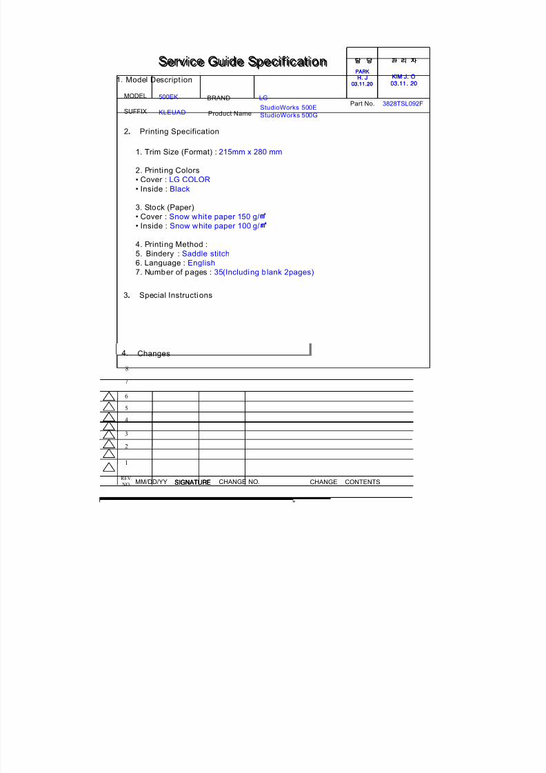
Model Descript ion
MODEL BRAND
Printing Specification
1. Trim Size (Format) : 215mm x 280 mm
2. Printing Colors• Cover : LG COLOR•
Inside : Black
3. Stock (Paper)• Cover : Snow white paper 150 g/• Inside : Snow white paper 100 g/
4. Printing Method :5. Bindery : Saddle stitch6. Language : English7. Number of pages : 35(Including blank 2pages)
Part No.
1.
2 .
Service Guide SpecificationService Guide Specification
Changes4.
REV. NO. MM/DD/YY CHANGE NO. CHANGE CONTENTS
1
2
3
4
5
7
6
SUFFIX
500EK
KLEUAD
LG3828TSL092F
8
Special Instructi ons3 .
Product NameStudioWorks 500EStudioWorks 500G
8/13/2019 (500g.pdf
http://slidepdf.com/reader/full/500gpdf 2/33
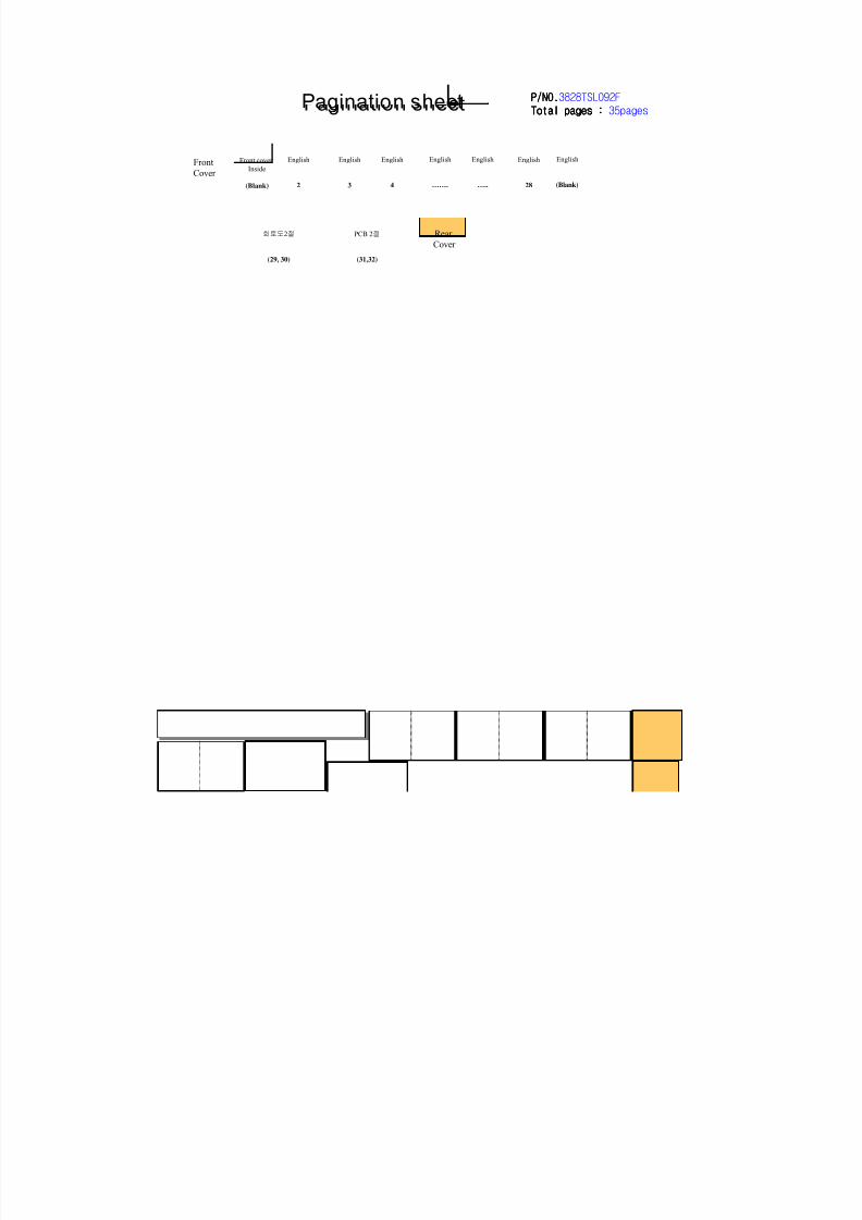
Pagination sheetPagination sheet
FrontCover
Front coverInside
(Blank)
English
2
English
3
English
4
English
…….
English
…..
English
28
English
(Blank)
2
(29, 30)
PCB 2
(31,32)
RearCover
8/13/2019 (500g.pdf
http://slidepdf.com/reader/full/500gpdf 3/33
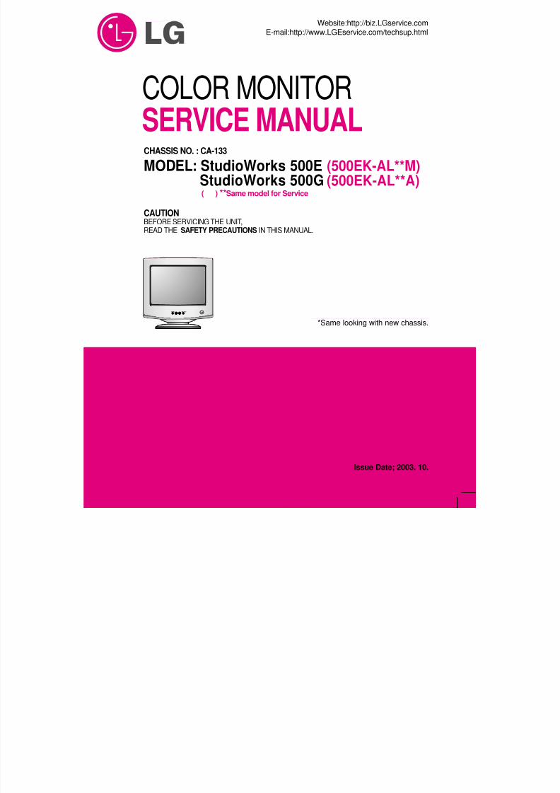
COLOR MONITORSERVICE MANUAL
Website:http://biz.LGservice.comE-mail:http://www.LGEservice.com/techsup.html
CAUTIONBEFORE SERVICING THE UNIT,READ THE SAFETY PRECAUTIONSIN THIS MANUAL.
MENU SELECT
MODEL: StudioWorks 500E (500EK-AL**M)StudioWorks 500G (500EK-AL**A)
CHASSIS NO. : CA-133
( ) **Same model for Service
*Same looking with new chassis.
Issue Date; 2003. 10.
8/13/2019 (500g.pdf
http://slidepdf.com/reader/full/500gpdf 4/33
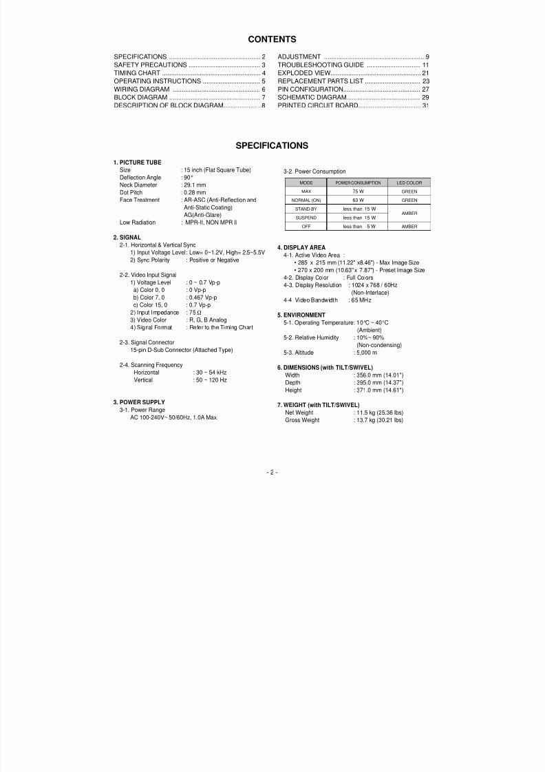
1. PICTURE TUBESize : 15 inch (Flat Square Tube)DefIection Angle : 90°Neck Diameter : 29.1 mmDot Pitch : 0.28 mmFace Treatment : AR-ASC (Anti-Reflection and
Anti-Static Coating)AG(Anti-Glare)
Low Radiation : MPR-II, NON MPR II
2. SIGNAL2-1. Horizontal & Vertical Sync
1) Input Voltage Level: Low= 0~1.2V, High= 2.5~5.5V2) Sync Polarity : Positive or Negative
2-2. Video Input Signal1) Voltage Level : 0 ~ 0.7 Vp-p
a) Color 0, 0 : 0 Vp-pb) Color 7, 0 : 0.467 Vp-pc) Color 15, 0 : 0.7 Vp-p
2) Input Impedance : 75 Ω
3) Video Color : R, G, B Analog4) Signal Format : Refer to the Timing Chart
2-3. Signal Connector15-pin D-Sub Connector (Attached Type)
2-4. Scanning FrequencyHorizontal : 30 ~ 54 kHz
Vertical : 50 ~ 120 Hz
3. POWER SUPPLY3-1. Power Range
AC 100-240V~ 50/60Hz, 1.0A Max.
3-2. Power Consumption
4. DISPLAY AREA4-1. Active Video Area :
• 285 x 215 mm (11.22" x8.46") - Max Image Size• 270 x 200 mm (10.63"x 7.87") - Preset Image Size
4-2. Display Color : Full Colors
4-3. Display Resolution : 1024 x 768 / 60Hz(Non-Interlace)
4-4. Video Bandwidth : 65 MHz
5. ENVIRONMENT5-1. Operating Temperature: 10°C ~ 40°C
(Ambient)5-2. Relative Humidity : 10%~ 90%
(Non-condensing)5-3. Altitude : 5,000 m
6. DIMENSIONS (with TILT/SWIVEL)Width : 356.0 mm (14.01")Depth : 395.0 mm (14.37")Height : 371.0 mm (14.61")
7. WEIGHT (with TILT/SWIVEL)Net Weight : 11.5 kg (25.36 lbs)Gross Weight : 13.7 kg (30.21 lbs)
CONTENTS
- 2 -
SPECIFICATIONS ................................................... 2SAFETY PRECAUTIONS ........................................ 3TIMING CHART ....................................................... 4OPERATING INSTRUCTIONS ................................ 5WIRING DIAGRAM ................................................. 6BLOCK DIAGRAM ................................................... 7DESCRIPTION OF BLOCK DIAGRAM................... ..8
ADJUSTMENT ........................................................ 9TROUBLESHOOTING GUIDE .............................. 11EXPLODED VIEW................................................... 21REPLACEMENT PARTS LIST ............................... 23PIN CONFIGURATION........................................... 27SCHEMATIC DIAGRAM......................................... 29PRINTED CIRCUIT BOARD................................... 31
SPECIFICATIONS
MODE
MAX
NORMAL (ON)
STAND-BY
SUSPEND
OFF
POWER CONSUMPTION
75 W
63 W
less than 15 W
less than 15 W
less than 5 W
LED COLOR
GREEN
GREEN
AMBER
AMBER
8/13/2019 (500g.pdf
http://slidepdf.com/reader/full/500gpdf 5/33
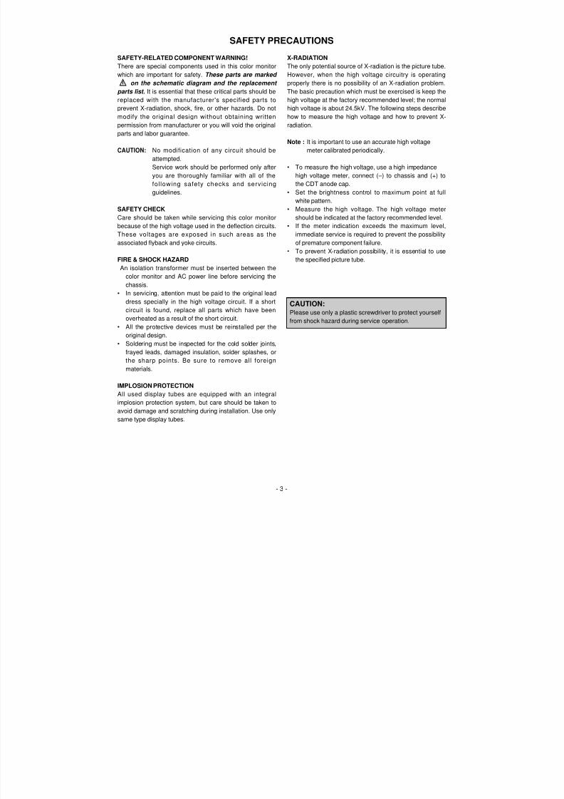
SAFETY-RELATED COMPONENT WARNING!There are special components used in this color monitorwhich are important for safety. These parts are marked
on the schematic diagram and the replacement parts list. It is essential that these critical parts should be
replaced with the manufacturer's specified parts toprevent X-radiation, shock, fire, or other hazards. Do notmodify the original design without obtaining writtenpermission from manufacturer or you will void the originalparts and labor guarantee.
CAUTION: No modification of any circuit should beattempted.Service work should be performed only afteryou are thoroughly familiar with all of thefollowing safety checks and servicingguidelines.
SAFETY CHECKCare should be taken while servicing this color monitorbecause of the high voltage used in the deflection circuits.These voltages are exposed in such areas as theassociated flyback and yoke circuits.
FIRE & SHOCK HAZARDAn isolation transformer must be inserted between the
color monitor and AC power line before servicing thechassis.
• In servicing, attention must be paid to the original leaddress specially in the high voltage circuit. If a shortcircuit is found, replace all parts which have beenoverheated as a result of the short circuit.
• All the protective devices must be reinstalled per theoriginal design.
• Soldering must be inspected for the cold solder joints,frayed leads, damaged insulation, solder splashes, orthe sharp points. Be sure to remove all foreignmaterials.
IMPLOSION PROTECTION
All used display tubes are equipped with an integralimplosion protection system, but care should be taken toavoid damage and scratching during installation. Use onlysame type display tubes.
X-RADIATIONThe only potential source of X-radiation is the picture tube.However, when the high voltage circuitry is operatingproperly there is no possibility of an X-radiation problem.The basic precaution which must be exercised is keep the
high voltage at the factory recommended level; the normalhigh voltage is about 24.5kV. The following steps describehow to measure the high voltage and how to prevent X-radiation.
Note : It is important to use an accurate high voltagemeter calibrated periodically.
• To measure the high voltage, use a high impedancehigh voltage meter, connect (–) to chassis and (+) tothe CDT anode cap.
• Set the brightness control to maximum point at fullwhite pattern.
• Measure the high voltage. The high voltage metershould be indicated at the factory recommended level.
• If the meter indication exceeds the maximum level,immediate service is required to prevent the possibilityof premature component failure.
• To prevent X-radiation possibility, it is essential to usethe specified picture tube.
CAUTION:Please use only a plastic screwdriver to protect yourselffrom shock hazard during service operation.
SAFETY PRECAUTIONS
- 3 -
8/13/2019 (500g.pdf
http://slidepdf.com/reader/full/500gpdf 6/33
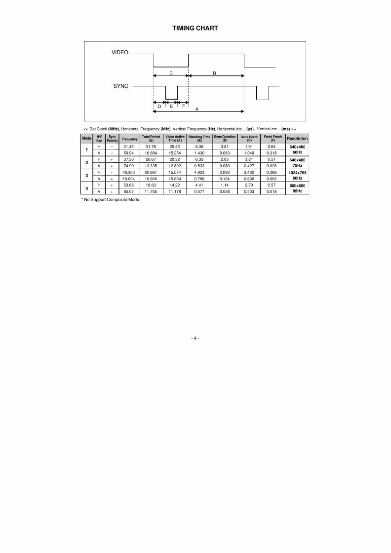
TIMING CHART
- 4 -
VIDEO
SYNC
C
ED FA
B
H – 31.47 31.78 25.42 6.36 3.81 1.91 0.64
V – 59.94 16.684 15.254 1.430 0.063 1.049 0.318
H + 37.50 26.67 20.32 6.35 2.03 3.81 0.51
V + 74.99 13.335 12.802 0.533 0.080 0.427 0.026
H + 48.363 20.667 15.574 4.923 2.092 2.462 0.369
V + 60.004 16.666 15.880 0.786 0.124 0.600 0.062
H + 53.68 18.63 14.22 4.41 1.14 2.70 0.57
V + 85.07 11.755 11.178 0.577 0.056 0.503 0.018
Mode H/VSort
1
2
3
4
640x48060Hz
1024x76860Hz
800x60085Hz
640x48075Hz
<< Dot Clock (MHz), Horizontal Frequency (kHz) , Vertical Frequency (Hz) , Horizontal etc... (µs) , Vertical etc... (ms) >>
* No Support Composite Mode.
SyncPolarity Frequency Total Period(E) Video ActiveTime (A) Sync Duration(D)Blanking Time
(B)Back Porch(C) Front Porch(F) Resolution
8/13/2019 (500g.pdf
http://slidepdf.com/reader/full/500gpdf 7/33
- 5 -
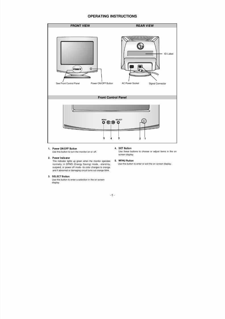
OPERATING INSTRUCTIONS
MENU SELECT
FRONT VIEW REAR VIEW
AC Power Socket Signal Connector
ID Label
Power ON/OFF ButtonSee Front Control Panel
Front Control Panel
1. Power ON/OFF ButtonUse this button to turn the monitor on or off.
2. Power IndicatorThis indicator lights up green when the monitor operatesnormally; in DPMS (Energy Saving) mode, - stand-by,suspend, or power off mode - its color changes to orange,and if abnormal or damaging circuit turns out orange blink.
3. SELECT ButtonUse this button to enter a selection in the on screendisplay.
4. SET ButtonUse these buttons to choose or adjust items in the onscreen display.
5. MENU ButtonUse this button to enter or exit the on screen display.
MENU SELECT
1345 2
8/13/2019 (500g.pdf
http://slidepdf.com/reader/full/500gpdf 8/33
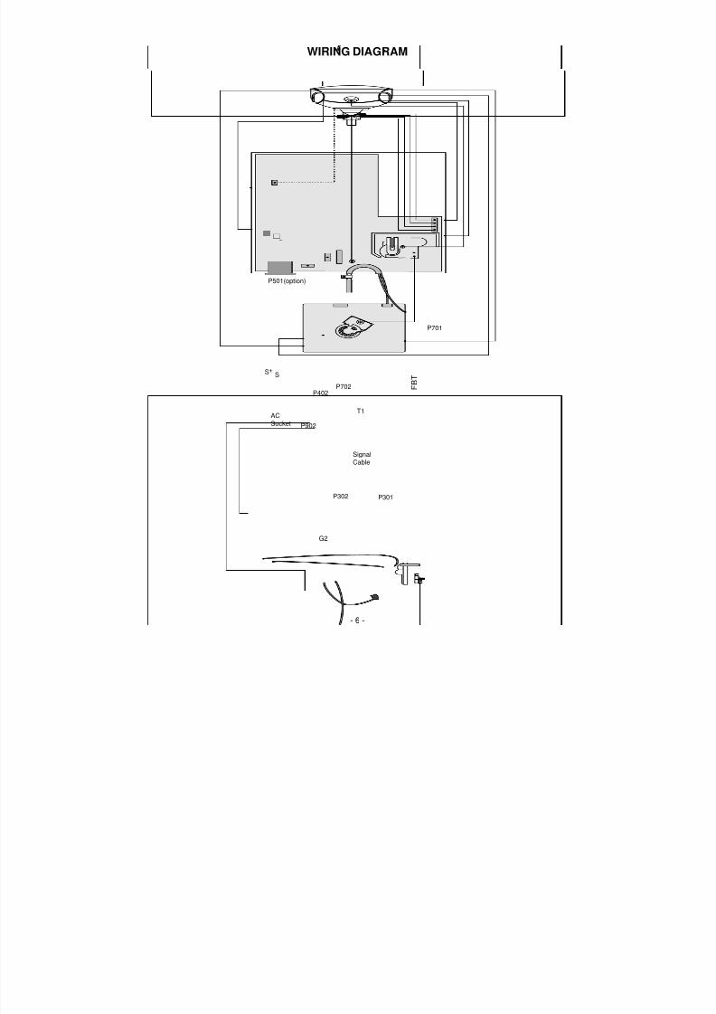
WIRING DIAGRAM
- 6 -
P501(option)
P301P302
G2
P702
P701
T1
P402
P902
S+S
SignalCable
ACSocket
F B T
8/13/2019 (500g.pdf
http://slidepdf.com/reader/full/500gpdf 9/33
BLOCK DIAGRAM
- 7 -
I n p u
t_ p o w e r
1 0 0 ~ 2 4 0 V A C
( 5 0 / 6 0 H z )
L i n e
F i l t e r
D e g a u s s i n g
C i r c u i t
[ O S D C o n
t r o l ]
P o w e r
C o n
t r o l
( I C 9 0 1 )
T I L T
C o n
t r o l
C i r c u i t
6 . 3 V
1 5 V
E 2 P R O M
( I C 4 0 2 )
5 V
H - s y n c
S i g n a l
V - s y n c
S i g n a l
I 2 C D A T A ( S D A )
I 2 C C L O C K ( S C L )
V I D E O
O S D + p r e_
A m p
( I C 3 0 2 )
S i g n a l
c a b l e
R G B
V I D E O
M a i n
_ A m p
( I C 3 0 3 )
H / V S y n c
P r o c e s s o r
( I C 7 0 1 )
T D A 4 8 4 1
V - o u
t
( I C 6 0 1 )
T D A 4 8 6 7 J
H - o u
t
( Q 7 0 6 )
H - L
i n e a r i t y
C o r r e c t i o n
C i r c u
i t
X - R
A Y
P r o
t e c t i o n
C i r c u
i t
V e r t i c a l
B l a n k i n g ,
- 1 6 0 V
1 5 V
D / D
F e e d B a c k
3 0 V
1 2 V
M I C O M
( I C 4 0 1 )
S C L / S D A
H / V s y n c
P W M c o n t r o l s
i g n a l
1 5 V
1 5 V
5 0 V
D Y
C D T
H e a t e r
( 6 . 3 V )
I 2 C
I 2 C
I 2 C H / V
S y n c
Screen
H . V
R / G / B
B i a s
R / G / B
C o n
t r a s t
H - D r i v e
B - D r i v e
B +
1 5 V
B R I G H T N E S S / C O N T R A S T
C O L O R C U R V E
H / V P O S I T I O N
H / V S I Z E
S P C C
T R A P I Z O D E
P I N B A L A N C E
P A R A L L E L O G R A M
T I L T
T O P C O R N E R
B O T T O M C O R N E R
R E C A L L
D E G A U S S I N G
M O I R E
L A N G U A G E
R E S E T
O S D T I M E
D P M C o n
t r o l
C i r c u i t
6 . 3 V
1 5 V
8 0 V
V o l t a g e
f e e d b a c k
V o l t a g e f e e d b a c k
D e g a u s s i n g
C o
i l
Dynamic FocusStatic Focus
T I L T
C o
i l
5 0 V 8 0 V
1 5 V
G 2 G 1
D C / D C C o n v e r t e r
F B T
( T 7 0 1 )
R e g u
l a t i o n
C i r c u i t
S M P S
( T 9 0 1 )
5 V
1 5 V C
U T - O F F I C
( I C 3 0 4 )
5 V
A u t o
B e a m
L i m i t
( O p t i o n )
8/13/2019 (500g.pdf
http://slidepdf.com/reader/full/500gpdf 10/33
DESCRIPTION OF BLOCK DIAGRAM
1. Line Filter & Associated CircuitThis is used for suppressing noise of power input lineflowing into the monitor and/or some noise generated inthe monitor flowing out through the power input line.That is to say,this circuit prevents interference betweenthe monitor and other electric appliance.
2. Degaussing Circuit Coil.The degaussing circuit consists of the degaussing coil,the PTC(Positive Temperature Coefficient) thermistr(TH901), and the relay(RL901). This circuit eliminateabnormal color of the screen automatically bydegaussing the shadow mask in the CRT during turningon the power switch.When you need to degaussing inusing the monitor,select DEGAUSS on the OSD menu.
3. SMPS(Switching Mode Power Supply).This circuit is working of 90~264V AC(50/60Hz).The operation procecedure is as below:1) AC input voltage is rectified and smoothed by the
bridge diodes(D900) and the capacitor.2) The rectified voltage(DC) is applied to the primarycoil of the transform(T901).
3) The control IC(IC901) generates switching pulse toturn on and off the primary coil of the transformer(T901) repeatedly.
4) Depending on turn ration of the transformer,thesecondary voltage appear at the secondary coils ofthe transformer(T901).
5) These secondary voltage are rectified by each diode(D941,D951,D961,D971,D942) and operate othercircuit.(horizontal and vertical deflection,videoamplifer,...etc.)
4. X-ray Protection CircuitWhen the high voltage reaches to 29kV in an abnormalstate), voltage of IC401(MICOM) pin 35 come to about2.5V.Then MICOM control IC701 (Deflection controller)tostophorizontal drive pulse and stop horizontal deflection.
5. Microprocessor Control CircuitThe operating procedure of MICOM(Microprocessor)and its associating circuit is as fallow:1) Horizontal and Vertical sync signals are supplied
from the signabl cable.2) Microprocessor(IC401) discriminates the operating
mode from the sync polarity and resolution.3) The Micom sets operating mode and offers the
controlled data.(H-Size,H-Position,V-Size,...)4) The controlled data of each mode is stored in itself.5) User can adjust screen condition by each OSD
function.the data of the adjusted condition is stored inEEPROM(IC402).
6. Horizontal and Vertical OscillationThis circuit generates the horizontal pulse and thevertical pulse by taking the H and V sync signal.This circuit consists of the H/V processor(IC701) andthe associate circuit.
7. D/D(DC to DC) ConverterThis circuit supplies DC voltage to the horizontaldeflection output circuit by increasing DC 50V which isthe secdonary voltage of the SMPS in accordance withthe input horizontal sync signal.
8. Side-Pincushion & Trapezoid Correction CircuitThis circuit improve the side-pincushion and thetrapezoid distortion of the screen by mixing parabolaand saw-tooth wave to output of the horizontaldeflection D/D converter which is used for the supplyvoltage (B + ) of the deflection circuit.
9. Horizontal Deflection Output CircuitThis circuit makes the horizontal deflection by supplyingthe saw-tooth current to the horizontal deflection yoke.
10.High Voltage Output & FBT(Flyback Transformer)The high voltage output circuit is used for generatingpulse to the primry coil of the FBT(Flyback
Transformer(T701)). A boosted voltage about 24.5kV)appears at the secondary of the FBT and it is suppliesdto the anode, focus, and screen voltage of the CRT.
11. H-Linearity Correction CircuitThis circuit corrects the horizontal linearity for eachhorizontal sync frequency.
12.Vertical Output CircuitThis circuit takes the vertical ramp wave from the IC701and performs the vertical deflection by supplying thesaw-tooth current to the vertical deflection yoke.
13.H & V Blanking and Brightness ControlBlanking circuit eliminate retrace line by supplyingnegatinve pulse to the G1 of the CRT. And Brightnesscontrol uses the R/G/B cut-off DC Level by IIC line.
14.Image Rotation(Tilt)Circuit-OptionThis circuit corrects the tilts of the screen by supplyingthe image rotation signal to the tilt which is attachednear the deflection yoke of the CRT.
15.Video Pre-AMP CircuitThis circuit amplifies the analog video signal from 0-0.7V to 0-4V. It is operated by taking the clamp,R,G,Bdrive and contrast signal from the MICOM(IC401).
16.Video Output AMP CircuitThis the circuit amplifies the video signal which comesfrom the video pre-amp circuit and amplifies it to appliedthe CRT cathode.
- 8 -
8/13/2019 (500g.pdf
http://slidepdf.com/reader/full/500gpdf 11/33
- 9 -
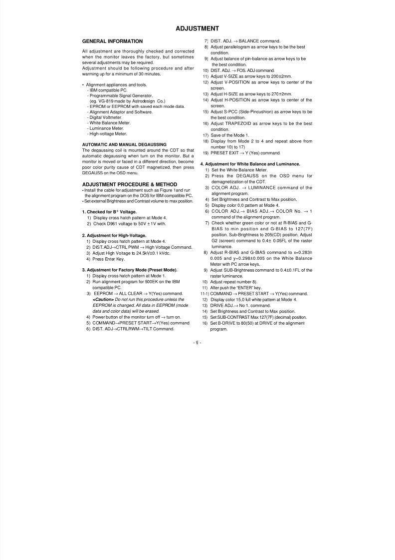
ADJUSTMENT
GENERAL INFORMATION
All adjustment are thoroughly checked and correctedwhen the monitor leaves the factory, but sometimesseveral adjustments may be required.
Adjustment should be following procedure and afterwarming up for a minimum of 30 minutes.
• Alignment appliances and tools.- IBM compatible PC.- Programmable Signal Generator.
(eg. VG-819 made by Astrodesign Co.)- EPROM or EEPROM with saved each mode data.- Alignment Adaptor and Software.- Digital Voltmeter.- White Balance Meter.- Luminance Meter.- High-voltage Meter.
AUTOMATIC AND MANUAL DEGAUSSINGThe degaussing coil is mounted around the CDT so thatautomatic degaussing when turn on the monitor. But amonitor is moved or faced in a different direction, becomepoor color purity cause of CDT magnetized, then pressDEGAUSS on the OSD menu.
ADJUSTMENT PROCEDURE & METHOD- Install the cable for adjustment such as Figure 1and run
the alignment program on the DOS for IBM compatible PC.- Set external Brightness and Contrast volume to max position.
1. Checked for B + Voltage.1) Display cross hatch pattern at Mode 4.2) Check D961 voltage to 50V ± 1V with.
2. Adjustment for High-Voltage.1) Display cross hatch pattern at Mode 4.2) DIST.ADJ → CTRL PWM → High Voltage Command.3) Adjust High Voltage to 24.5kV ± 0.1 kVdc.4) Press Enter Key.
3. Adjustment for Factory Mode (Preset Mode).
1) Display cross hatch pattern at Mode 1.2) Run alignment program for 500EK on the IBM
compatible PC.3) EEPROM → ALL CLEAR → Y(Yes) command.
<Caution> Do not run this procedure unless theEEPROM is changed. All data in EEPROM (modedata and color data) will be erased.
4) Power button of the monitor turn off → turn on.5) COMMAND → PRESET START → Y(Yes) command.6) DIST. ADJ → CTRLRWM → TILT Command.
7) DIST. ADJ. → BALANCE command.8) Adjust parallelogram as arrow keys to be the best
condition.9) Adjust balance of pin-balance as arrow keys to be
the best condition.10) DIST. ADJ. → FOS. ADJ command.11) Adjust V-SIZE as arrow keys to 200 ± 2mm.12) Adjust V-POSITION as arrow keys to center of the
screen.13) Adjust H-SIZE as arrow keys to 270 ± 2mm.14) Adjust H-POSITION as arrow keys to center of the
screen.15) Adjust S-PCC (Side-Pincushion) as arrow keys to be
the best condition.16) Adjust TRAPEZOID as arrow keys to be the best
condition.17) Save of the Mode 1.18) Display from Mode 2 to 4 and repeat above from
number 10) to 17)19) PRESET EXIT → Y (Yes) command.
4. Adjustment for White Balance and Luminance.1) Set the White Balance Meter.2) Press the DEGAUSS on the OSD menu for
demagnetization of the CDT.3) COLOR ADJ. → LUMINANCE command of the
alignment program.4) Set Brightness and Contrast to Max position.
5) Display color 0,0 pattern at Mode 4.6) COLOR ADJ. → BIAS ADJ. → COLOR No. → 1command of the alignment program.
7) Check whether green color or not at R-BIAS and G-BIAS to min position and G-BIAS to 127(7F)position. Sub-Brightness to 205(CD) position. AdjustG2 (screen) command to 0.4 ± 0.05FL of the rasterluminance.
8) Adjust R-BIAS and G-BIAS command to x=0.283 ±
0.005 and y=0.298 ± 0.005 on the White BalanceMeter with PC arrow keys.
9) Adjust SUB-Brightness command to 0.4 ± 0.1FL of the
raster luminance.10) Adjust repeat number 8).11) After push the “ENTER” key.
11-1) COMMAND→ PRESET START → Y(Yes) command.12) Display color 15,0 full white pattern at Mode 4.13) DRIVE ADJ. → No 1. command.14) Set Brightness and Contrast to Max position.15) Set SUB-CONTRAST Max 127(7F) (decimal) position.16) Set B-DRIVE to 80(50) at DRIVE of the alignment
program.

8/13/2019 (500g.pdf
http://slidepdf.com/reader/full/500gpdf 12/33
- 10 -
17-1) Adjust R-DRIVE and B-DRIVE command to whitebalance x=0.283 ± 0.003 and y=0.298 ± 0.003 on theWhite Balance Meter with PC arrow keys.
17-2) Display color 15,0 window pattern (70x70mm) at mode 4.18) Adjust SUB-CONTRAST command to 50 ± 2FL .
19) Display color 15,0 full white patten at Mode 4.20) Set Brightness and Contrast to Max position.21) COLOR ADJ. → LUMINANCE → ABL command.22) Adjust ABL to 32 ± 1FL of the luminance.23) After push the “ENTER” key, and “COMMAND →
PRESET EXIT → Y(Yes)” command.24) Exit from the program.
5. Input EDID Data.1) Display color 15,0 cross hatch pattern at Mode 4.2) EEPROM → Write EDID command and confirm
“EDID Write OK!!” message of monitor.3) Exit from the alignment program.4) Power switch OFF/ON for EDID data save.
6. Adjustment for Focus.1) Set the Brightness and Contrast to max position.2) Display H character in full screen at Mode 4.3) Adjust two Focus control on the FBT that focus
should be the best condition.
8/13/2019 (500g.pdf
http://slidepdf.com/reader/full/500gpdf 13/33
8/13/2019 (500g.pdf
http://slidepdf.com/reader/full/500gpdf 14/33
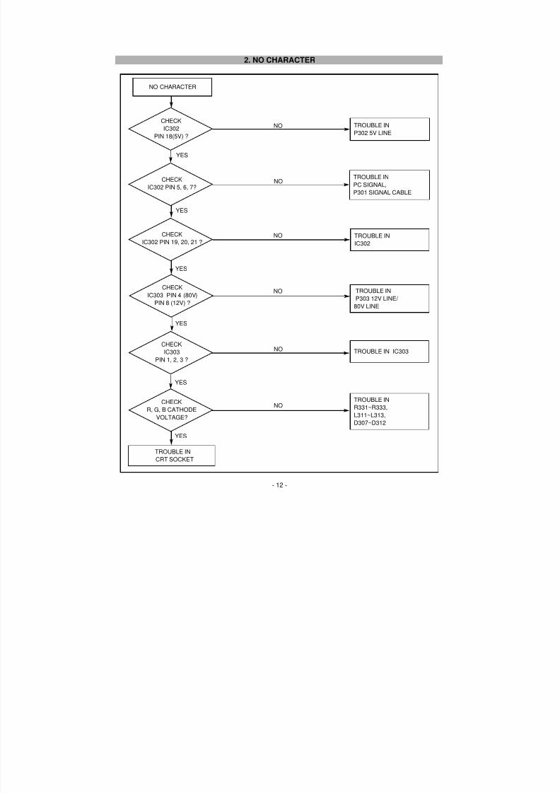
- 12 -
2. NO CHARACTER
NO CHARACTER
CHECKIC302
PIN 18(5V) ?
CHECKIC302 PIN 5, 6, 7?
CHECKIC302 PIN 19, 20, 21 ?
CHECKIC303
PIN 1, 2, 3 ?
CHECKIC303 PIN 4 (80V)
PIN 8 (12V) ?
TROUBLE INP302 5V LINE
TROUBLE INPC SIGNAL,P301 SIGNAL CABLE
TROUBLE INIC302
TROUBLE INP303 12V LINE/ 80V LINE
TROUBLE IN IC303
NO
YES
NO
NO
YES
YES
YES
YES
NO
NO
CHECKR, G, B CATHODE
VOLTAGE?
TROUBLE INR331~R333,L311~L313,D307~D312
TROUBLE INCRT SOCKET
YES
NO
8/13/2019 (500g.pdf
http://slidepdf.com/reader/full/500gpdf 15/33
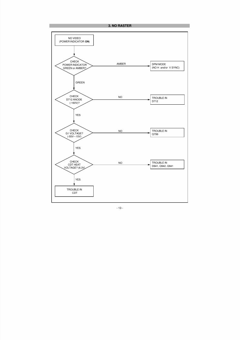
- 13 -
3. NO RASTER
NO VIDEO
(POWER INDICATOR ON)
CHECKPOWER INDICATORGREEN or AMBER?
CHECKD712 ANODE
(-160V)?
CHECKG1 VOLTAGE?
(-55V~-15V)
TROUBLE IND712
TROUBLE INQ799
DPM MODE(NO H and/or V SYNC)
AMBER
NO
GREEN
YES
NO
CHECKCDT HEAT
VOLTAGE? (6.3V)
TROUBLE IND941, Q942, Q941
YES
NO
TROUBLE INCDT
YES
8/13/2019 (500g.pdf
http://slidepdf.com/reader/full/500gpdf 16/33
- 14 -
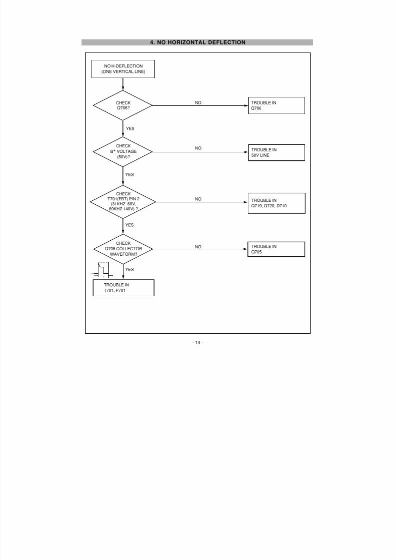
4. NO HORIZONTAL DEFLECTION
NO H-DEFLECTION(ONE VERTICAL LINE)
CHECKQ706?
CHECKB+ VOLTAGE
(50V)?
CHECKT701(FBT) PIN 2
(31KHZ 60V,69KHZ 140V) ?
CHECKQ705 COLLECTOR
WAVEFORM?
TROUBLE INQ706
TROUBLE IN50V LINE
TROUBLE IN
Q719, Q720, D710
TROUBLE INQ705
TROUBLE INT701, P701
NO
NO
YES
YES
YES
YES
NO
NO
0V
T
8/13/2019 (500g.pdf
http://slidepdf.com/reader/full/500gpdf 17/33
- 15 -
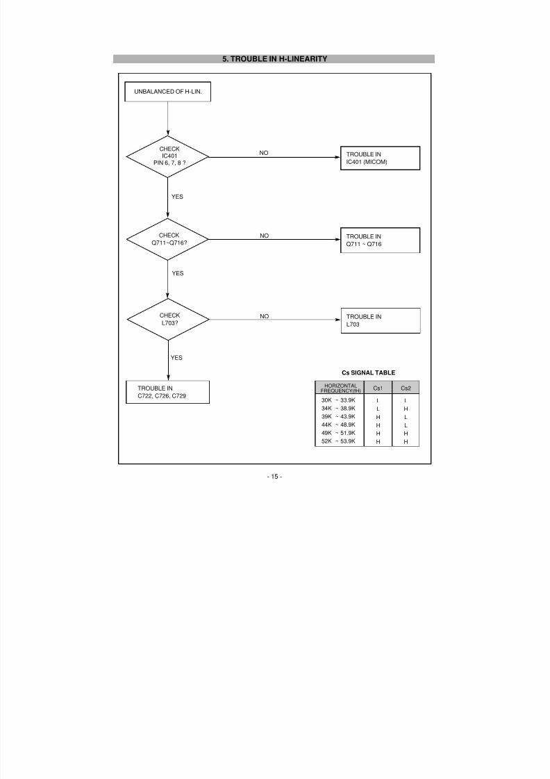
5. TROUBLE IN H-LINEARITY
UNBALANCED OF H-LIN.
CHECKIC401
PIN 6, 7, 8 ?
CHECKQ711~Q716?
CHECKL703?
TROUBLE INIC401 (MICOM)
TROUBLE INQ711 ~ Q716
TROUBLE INL703
TROUBLE INC722, C726, C729
NO
NO
NO
YES
YES
YES
Cs SIGNAL TABLE
HORIZONTALFREQUENCY(fH)
30K ~ 33.9K34K ~ 38.9K39K ~ 43.9K44K ~ 48.9K49K ~ 51.9K52K ~ 53.9K
Cs1
LLHHHH
Cs2
LHLLHH
8/13/2019 (500g.pdf
http://slidepdf.com/reader/full/500gpdf 18/33
- 16 -
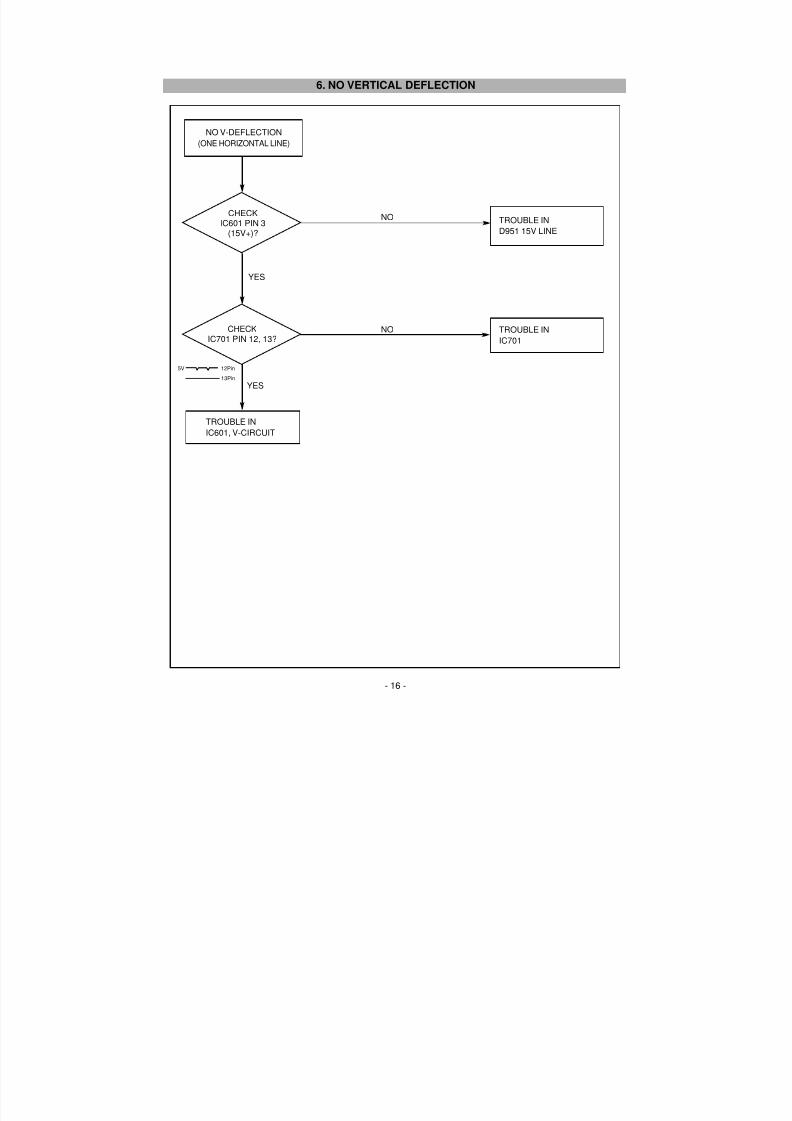
6. NO VERTICAL DEFLECTION
NO V-DEFLECTION(ONE HORIZONTAL LINE)
CHECKIC601 PIN 3
(15V+)?
CHECKIC701 PIN 12, 13?
TROUBLE IND951 15V LINE
TROUBLE INIC701
TROUBLE INIC601, V-CIRCUIT
NO
YES
YES
NO
5V 12Pin
13Pin
8/13/2019 (500g.pdf
http://slidepdf.com/reader/full/500gpdf 19/33
- 17 -
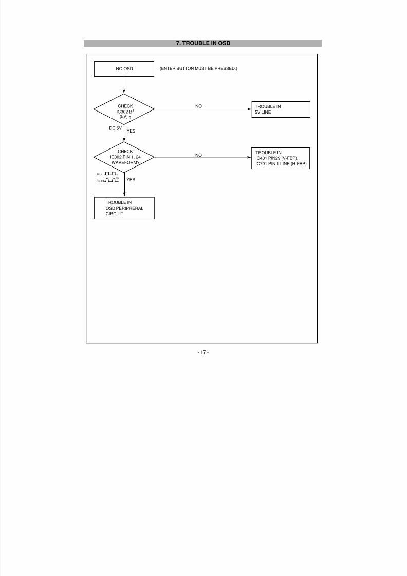
7. TROUBLE IN OSD
TROUBLE INOSD PERIPHERAL
CIRCUIT
NO OSD
TROUBLE IN5V LINE
TROUBLE INIC401 PIN29 (V-FBP),IC701 PIN 1 LINE (H-FBP)
NO
YESDC 5V
YES
NO
Pin 245V
Pin 1
CHECKIC302 B +
(5V) ?
(ENTER BUTTON MUST BE PRESSED.)
CHECKIC302 PIN 1, 24WAVEFORM?
8/13/2019 (500g.pdf
http://slidepdf.com/reader/full/500gpdf 20/33
- 18 -
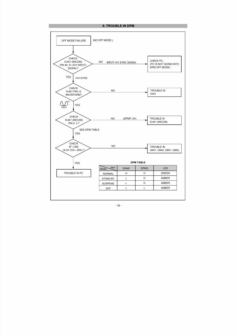
8. TROUBLE IN DPM
CHECKIC401 (MICOM)
PIN 30, 31 (H/V INPUT)SIGNAL?
CHECKIC401 PIN 12WAVEFORM?
CHECKIC401 (MICOM)
PIN 2, 3 ?
CHECKB+ LINE
(6.3V,15V+, 80V) ?
CHECK PC,(PC IS NOT GOING INTODPM OFF MODE)
TROUBLE INX401
TROUBLE INIC401 (MICOM)
TROUBLE INQ941, Q942, Q951, Q952,
TROUBLE IN PC
OFF MODE FAILURE
INPUT H/V SYNC SIGNAL
H/V SYNC
(NO OFF MODE.)
NO
NO
NO
NO (DPMF: 0V)
DPM TABLE
Mode Item
NORMAL
STAND-BY
SUSPEND
OFF
DPMF
H
L
L
L
LED
GREEN
AMBER
AMBER
AMBER
DPMS
H
H
H
L
YES
YES
SEE DPM TABLEYES
YES
5V
12MHz
8/13/2019 (500g.pdf
http://slidepdf.com/reader/full/500gpdf 21/33
- 19 -
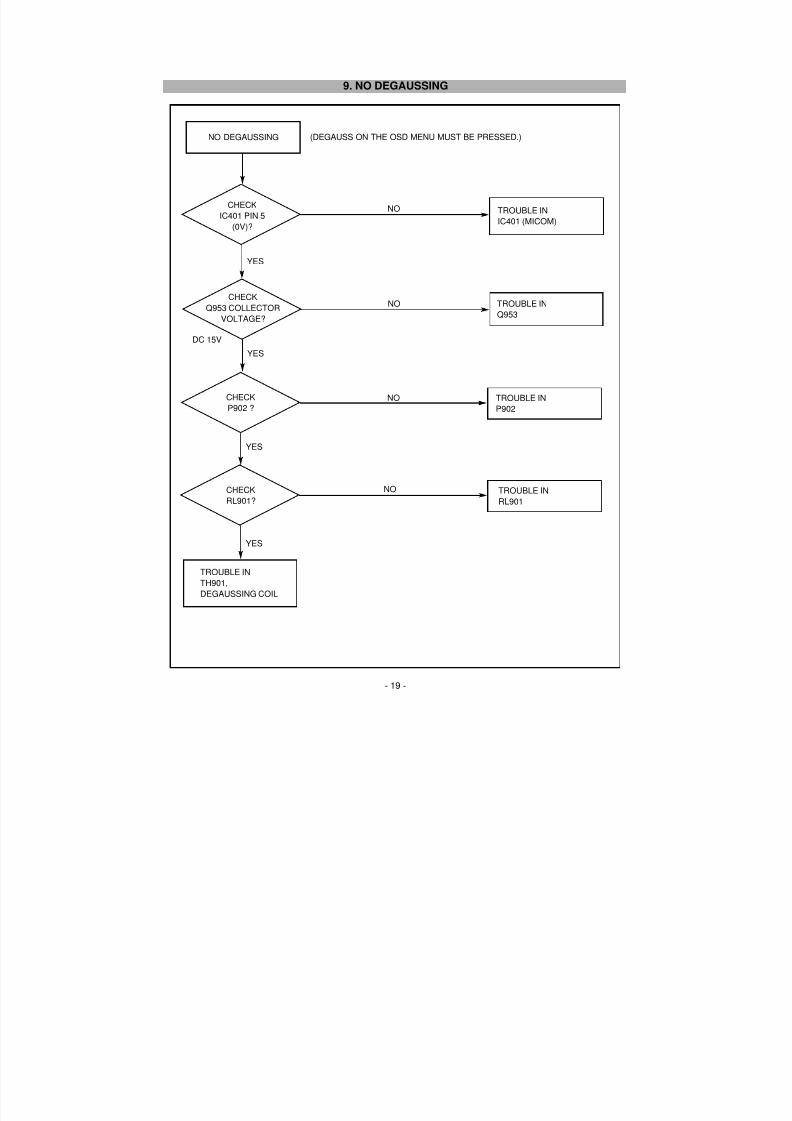
9. NO DEGAUSSING
CHECKIC401 PIN 5
(0V)?
CHECKQ953 COLLECTOR
VOLTAGE?
CHECKP902 ?
CHECKRL901?
TROUBLE INIC401 (MICOM)
TROUBLE INQ953
TROUBLE INP902
TROUBLE INRL901
TROUBLE INTH901,DEGAUSSING COIL
NO DEGAUSSING
DC 15V
NO
NO
NO
NO
YES
YES
YES
YES
(DEGAUSS ON THE OSD MENU MUST BE PRESSED.)
8/13/2019 (500g.pdf
http://slidepdf.com/reader/full/500gpdf 22/33
- 20 -
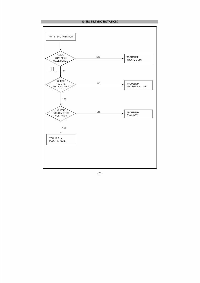
10. NO TILT (NO ROTATION)
NO TILT (NO ROTATION)
TROUBLE INIC401 ( MICOM)
TROUBLE IN15V LINE, 6.3V LINE
TROUBLE INQ501~Q503
TROUBLE INP501, TILT COIL
NO
YES
YES
YES
CHECK15V LINE
AND 6.3V LINE ?
CHECKQ503 EMITTER
VOLTAGE ?
NO
NO
CHECKIC401 PIN21
WAVE FORM ?
8/13/2019 (500g.pdf
http://slidepdf.com/reader/full/500gpdf 23/33
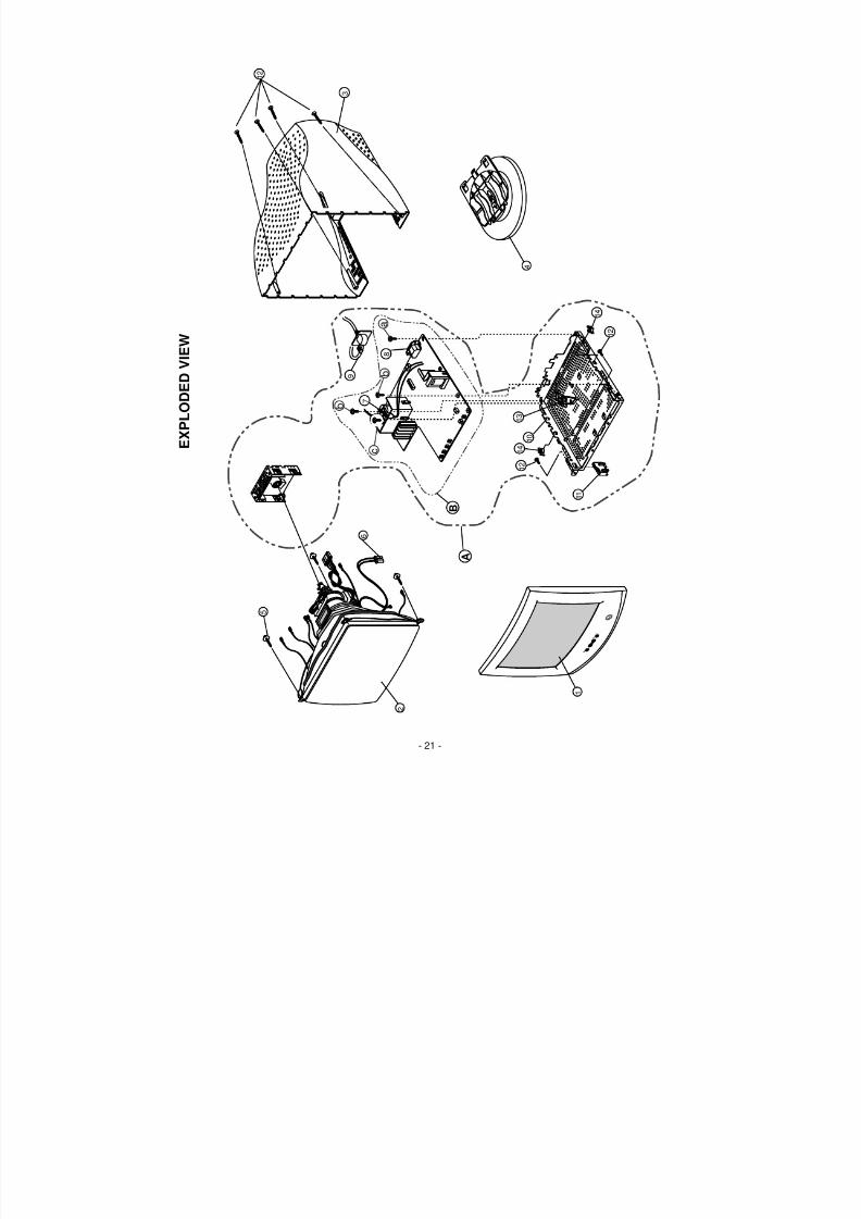
E X P L O D E D V I E W
- 21 -
1 0
A
M E
N U
S E
L E
C T
1 2
1
4
1 2
1 1
1 2
1 3
3
2
6
5
8
B
7
9
a
b
c
b
1 4
1 4
8/13/2019 (500g.pdf
http://slidepdf.com/reader/full/500gpdf 24/33
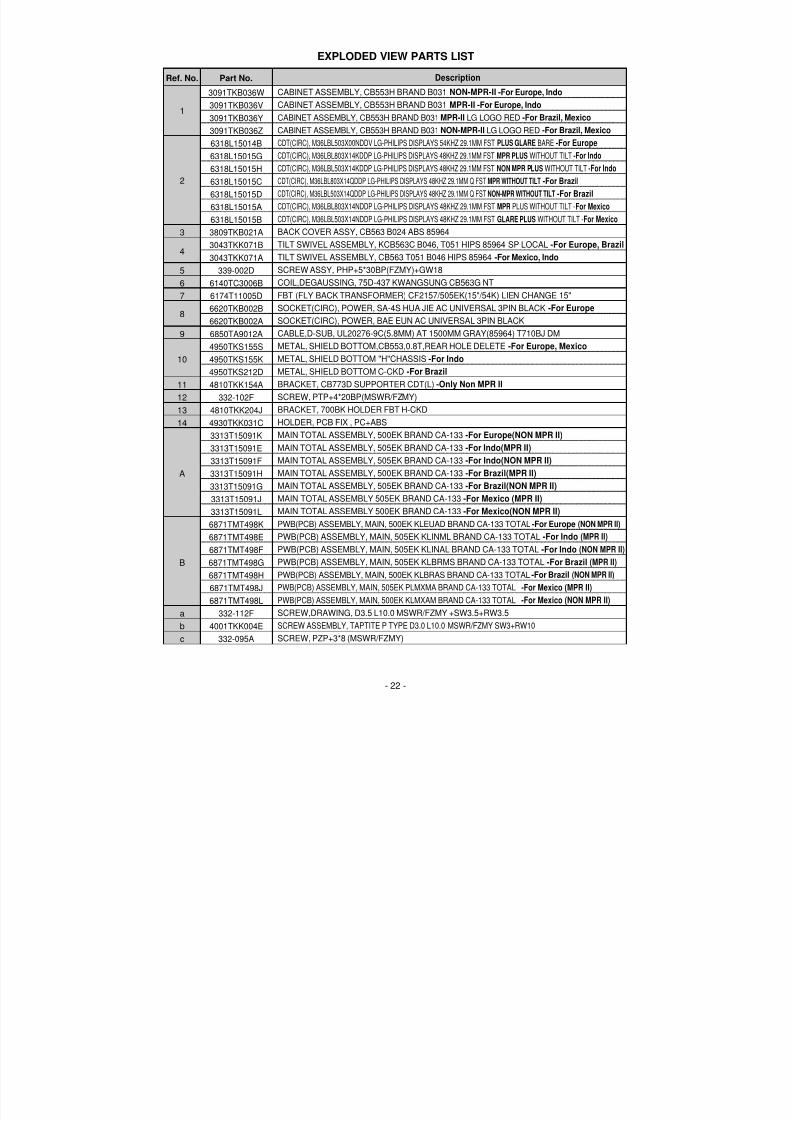
EXPLODED VIEW PARTS LIST
- 22 -
Part No.
3091TKB036W3091TKB036V3091TKB036Y3091TKB036Z6318L15014B6318L15015G6318L15015H6318L15015C6318L15015D6318L15015A6318L15015B3809TKB021A3043TKK071B3043TKK071A
339-002D6140TC3006B6174T11005D6620TKB002B6620TKB002A6850TA9012A4950TKS155S4950TKS155K4950TKS212D4810TKK154A
332-102F4810TKK204J4930TKK031C3313T15091K3313T15091E3313T15091F3313T15091H3313T15091G3313T15091J3313T15091L6871TMT498K6871TMT498E
6871TMT498F6871TMT498G6871TMT498H6871TMT498J6871TMT498L
332-112F4001TKK004E
332-095A
Ref. No.
1
2
3
4
567
8
9
10
11121314
A
B
abc
Description
CABINET ASSEMBLY, CB553H BRAND B031 NON-MPR-II-For Europe, IndoCABINET ASSEMBLY, CB553H BRAND B031 MPR-II-For Europe, IndoCABINET ASSEMBLY, CB553H BRAND B031 MPR-IILG LOGO RED -For Brazil, MexicoCABINET ASSEMBLY, CB553H BRAND B031 NON-MPR-IILG LOGO RED -For Brazil, MexicoCDT(CIRC), M36LBL503X00NDDV LG-PHILIPS DISPLAYS 54KHZ 29.1MM FSTPLUS GLAREBARE-For EuropeCDT(CIRC), M36LBL803X14KDDP LG-PHILIPS DISPLAYS 48KHZ 29.1MM FSTMPR PLUS WITHOUT TILT-For Indo
CDT(CIRC), M36LBL503X14KDDP LG-PHILIPS DISPLAYS 48KHZ 29.1MM FSTNON MPR PLUSWITHOUT TILT-For Indo
CDT(CIRC), M36LBL803X14QDDP LG-PHILIPS DISPLAYS 48KHZ 29.1MM Q FSTMPR WITHOUT TILT-For BrazilCDT(CIRC), M36LBL503X14QDDP LG-PHILIPS DISPLAYS 48KHZ 29.1MM Q FSTNON-MPR WITHOUT TILT-For BrazilCDT(CIRC), M36LBL803X14NDDP LG-PHILIPS DISPLAYS 48KHZ 29.1MM FSTMPR PLUS WITHOUT TILT -For Mexico
CDT(CIRC), M36LBL503X14NDDP LG-PHILIPS DISPLAYS 48KHZ 29.1MM FSTGLARE PLUSWITHOUT TILT -For Mexico
BACK COVER ASSY, CB563 B024 ABS 85964TILT SWIVEL ASSEMBLY, KCB563C B046, T051 HIPS 85964 SP LOCAL -For Europe, BrazilTILT SWIVEL ASSEMBLY, CB563 T051 B046 HIPS 85964 -For Mexico, IndoSCREW ASSY, PHP+5*30BP(FZMY)+GW18COIL,DEGAUSSING, 75D-437 KWANGSUNG CB563G NTFBT (FLY BACK TRANSFORMER) CF2157/505EK(15"/54K) LIEN CHANGE 15"SOCKET(CIRC), POWER, SA-4S HUA JIE AC UNIVERSAL 3PIN BLACK -For EuropeSOCKET(CIRC), POWER, BAE EUN AC UNIVERSAL 3PIN BLACKCABLE,D-SUB, UL20276-9C(5.8MM) AT 1500MM GRAY(85964) T710BJ DMMETAL, SHIELD BOTTOM,CB553,0.8T,REAR HOLE DELETE -For Europe, MexicoMETAL, SHIELD BOTTOM "H"CHASSIS -For IndoMETAL, SHIELD BOTTOM C-CKD -For BrazilBRACKET, CB773D SUPPORTER CDT(L) -Only Non MPR IISCREW, PTP+4*20BP(MSWR/FZMY)BRACKET, 700BK HOLDER FBT H-CKDHOLDER, PCB FIX , PC+ABSMAIN TOTAL ASSEMBLY, 500EK BRAND CA-133 -For Europe(NON MPR II)MAIN TOTAL ASSEMBLY, 505EK BRAND CA-133 -For Indo(MPR II)MAIN TOTAL ASSEMBLY, 505EK BRAND CA-133 -For Indo(NON MPR II)MAIN TOTAL ASSEMBLY, 500EK BRAND CA-133 -For Brazil(MPR II)MAIN TOTAL ASSEMBLY, 505EK BRAND CA-133 -For Brazil(NON MPR II)MAIN TOTAL ASSEMBLY 505EK BRAND CA-133 -For Mexico (MPR II)MAIN TOTAL ASSEMBLY 500EK BRAND CA-133 -For Mexico(NON MPR II)PWB(PCB) ASSEMBLY, MAIN, 500EK KLEUAD BRAND CA-133 TOTAL -For Europe (NON MPR II)PWB(PCB) ASSEMBLY, MAIN, 505EK KLINML BRAND CA-133 TOTAL -For Indo (MPR II)PWB(PCB) ASSEMBLY, MAIN, 505EK KLINAL BRAND CA-133 TOTAL
-For Indo (NON MPR II)PWB(PCB) ASSEMBLY, MAIN, 505EK KLBRMS BRAND CA-133 TOTAL -For Brazil (MPR II)PWB(PCB) ASSEMBLY, MAIN, 500EK KLBRAS BRAND CA-133 TOTAL -For Brazil (NON MPR II)PWB(PCB) ASSEMBLY, MAIN, 505EK PLMXMA BRAND CA-133 TOTAL-For Mexico (MPR II)PWB(PCB) ASSEMBLY, MAIN, 500EK KLMXAM BRAND CA-133 TOTAL-For Mexico (NON MPR II)SCREW,DRAWING, D3.5 L10.0 MSWR/FZMY +SW3.5+RW3.5SCREW ASSEMBLY, TAPTITE P TYPE D3.0 L10.0 MSWR/FZMY SW3+RW10SCREW, PZP+3*8 (MSWR/FZMY)
8/13/2019 (500g.pdf
http://slidepdf.com/reader/full/500gpdf 25/33
- 23 -
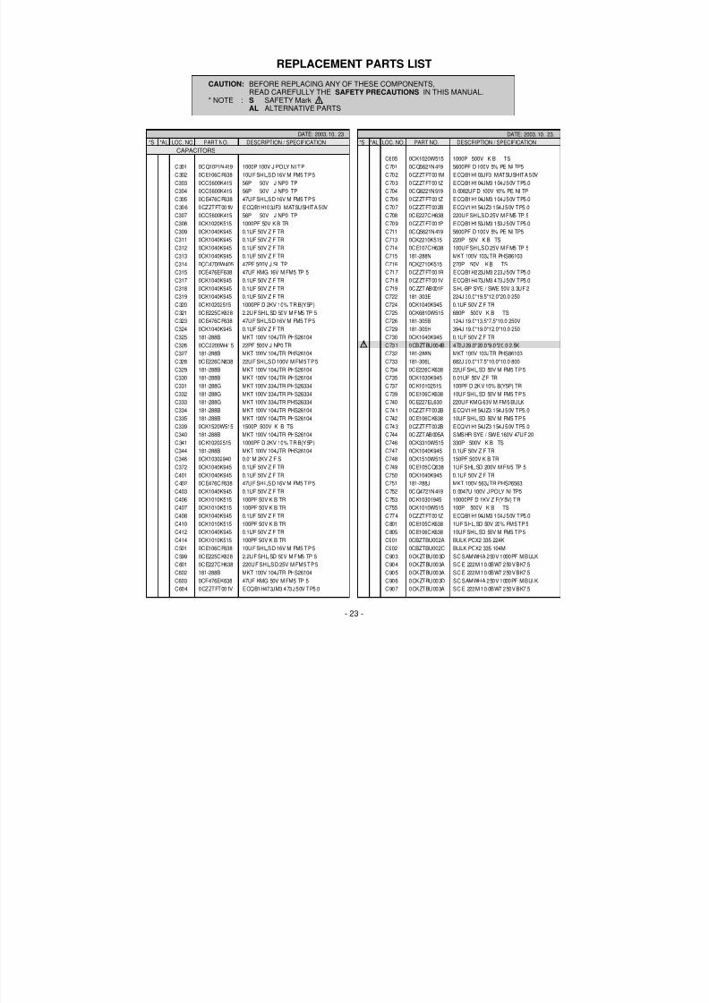
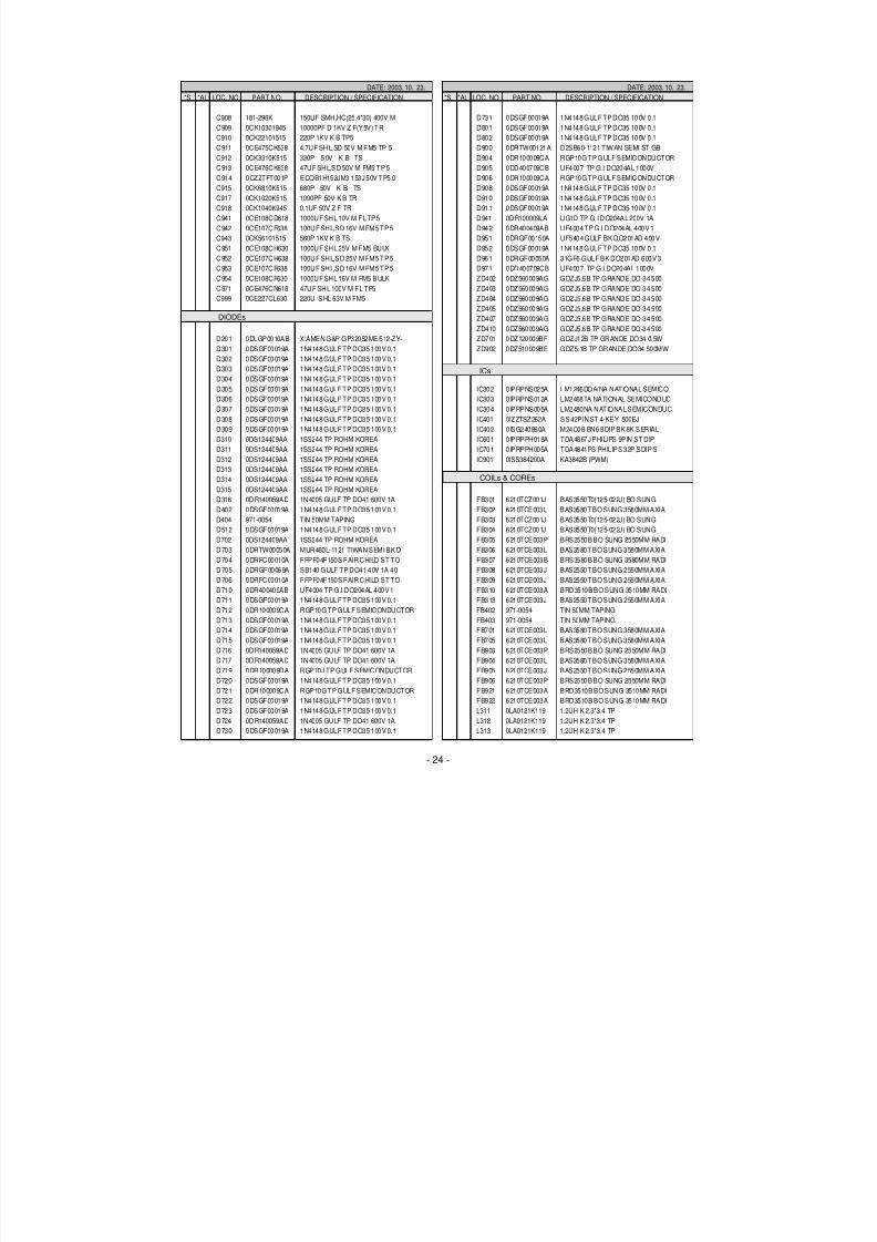
DATE: 2003. 10. 23*S *AL LOC. NO. PART NO. DESCRIPTION / SPECIFICATION
C301 0CQ1021N419 1000P 100V J POLY NI TPC302 0CE106CF638 10UF SHL,SD 16V M FM5 TP 5C303 0CC5600K415 56P 50V J NP0 TPC304 0CC5600K415 56P 50V J NP0 TPC305 0CE476CF638 47UF SHL,SD 16V M FM5 TP 5C306 0CZZTFT001M ECQB1H103JF3 MATSUSHITA 50VC307 0CC5600K415 56P 50V J NP0 TPC308 0CK1020K515 1000PF 50V K B TRC309 0CK1040K945 0.1UF 50V Z F TRC311 0CK1040K945 0.1UF 50V Z F TR
C312 0CK1040K945 0.1UF 50V Z F TRC313 0CK1040K945 0.1UF 50V Z F TRC314 0CC4700W405 47PF 500V J SL TPC315 0CE476EF638 47UF KMG 16V M FM5 TP 5C317 0CK1040K945 0.1UF 50V Z F TRC318 0CK1040K945 0.1UF 50V Z F TRC319 0CK1040K945 0.1UF 50V Z F TRC320 0CK10202515 1000PF D 2KV 10% TR B(Y5P)C321 0CE225CK638 2.2UF SHL,SD 50V M FM5 TP 5C323 0CE476CF638 47UF SHL,SD 16V M FM5 TP 5C324 0CK1040K945 0.1UF 50V Z F TRC325 181-288B MKT 100V 104JTR PHS26104C326 0CC2200W415 22PF 500V J NP0 TRC327 181-288B MKT 100V 104JTR PHS26104C328 0CE226CN638 22UF SHL,SD 100V M FM5 TP 5
C329 181-288B MKT 100V 104JTR PHS26104C330 181-288B MKT 100V 104JTR PHS26104C331 181-288G MKT 100V 334JTR PHS26334C332 181-288G MKT 100V 334JTR PHS26334C333 181-288G MKT 100V 334JTR PHS26334C334 181-288B MKT 100V 104JTR PHS26104C335 181-288B MKT 100V 104JTR PHS26104C339 0CK1520W515 1500P 500V K B TSC340 181-288B MKT 100V 104JTR PHS26104C341 0CK10202515 1000PF D 2KV 10% TR B(Y5P)C344 181-288B MKT 100V 104JTR PHS26104C346 0CK10302940 0.01M 2KV Z F SC372 0CK1040K945 0.1UF 50V Z F TRC401 0CK1040K945 0.1UF 50V Z F TRC402 0CE476CF638 47UF SHL,SD 16V M FM5 TP 5C403 0CK1040K945 0.1UF 50V Z F TRC406 0CK1010K515 100PF 50V K B TRC407 0CK1010K515 100PF 50V K B TRC408 0CK1040K945 0.1UF 50V Z F TRC410 0CK1010K515 100PF 50V K B TRC412 0CK1040K945 0.1UF 50V Z F TRC414 0CK1010K515 100PF 50V K B TRC501 0CE106CF638 10UF SHL,SD 16V M FM5 TP 5C599 0CE225CK638 2.2UF SHL,SD 50V M FM5 TP 5C601 0CE227CH638 220UF SHL,SD 25V M FM5 TP 5C602 181-288B MKT 100V 104JTR PHS26104C603 0CE476EK638 47UF KMG 50V M FM5 TP 5C604 0CZZTFT001V ECQB1H473JM3 473J 50V TP5.0
DATE: 2003. 10. 23.*S *AL LOC. NO. PART NO. DESCRIPTION / SPECIFICATION
C605 0CK1020W515 1000P 500V K B TSC701 0CQ5621N419 5600PF D 100V 5% PE NI TP5C702 0CZZTFT001M ECQB1H103JF3 MATSUSHITA 50VC703 0CZZTFT001Z ECQB1H104JM3 104J 50V TP5.0C704 0CQ8221N519 0.0082UF D 100V 10% PE NI TPC706 0CZZTFT001Z ECQB1H104JM3 104J 50V TP5.0C707 0CZZTFT002B ECQV1H154JZ3 154J 50V TP5.0C708 0CE227CH638 220UF SHL,SD 25V M FM5 TP 5C709 0CZZTFT001P ECQB1H153JM3 153J 50V TP5.0C711 0CQ5621N419 5600PF D 100V 5% PE NI TP5C713 0CK2210K515 220P 50V K B TS
C714 0CE107CH638 100UF SHL,SD 25V M FM5 TP 5C715 181-288N MKT 100V 103JTR PHS86103C716 0CK2710K515 270P 50V K B TSC717 0CZZTFT001R ECQB1H223JM3 223J 50V TP5.0C718 0CZZTFT001V ECQB1H473JM3 473J 50V TP5.0C719 0CZZTAB001F SHL-BP SYE / SWE 50V 3.3UF 2C722 181-303E 224J 30.0*19.5*12.0*20.0 250C724 0CK1040K945 0.1UF 50V Z F TRC725 0CK6810W515 680P 500V K B TSC726 181-305B 124J 19.0*13.5*7.5*10.0 250VC729 181-305H 394J 19.0*19.0*12.0*10.0 250C730 0CK1040K945 0.1UF 50V Z F TRC731 0CBZTBU004B 472J 29.0*20.0*9.0*20.0 2.5KC732 181-288N MKT 100V 103JTR PHS86103C733 181-306L 682J 20.0*17.5*10.0*10.0 800
C734 0CE226CK638 22UF SHL,SD 50V M FM5 TP 5C735 0CK1030K945 0.01UF 50V Z F TRC737 0CK10102515 100PF D 2KV 10% B(Y5P) TRC739 0CE106CK638 10UF SHL,SD 50V M FM5 TP 5C740 0CE227EL630 220UF KMG 63V M FM5 BULKC741 0CZZTFT002B ECQV1H154JZ3 154J 50V TP5.0C742 0CE106CK638 10UF SHL,SD 50V M FM5 TP 5C743 0CZZTFT002B ECQV1H154JZ3 154J 50V TP5.0C744 0CZZTAB005A SMSHR SYE / SWE 160V 47UF 20C746 0CK3310W515 330P 500V K B TSC747 0CK1040K945 0.1UF 50V Z F TRC748 0CK1510W515 150PF 500V K B TRC749 0CE105CQ638 1UF SHL,SD 200V M FM5 TP 5C750 0CK1040K945 0.1UF 50V Z F TRC751 181-288J MKT 100V 563JTR PHS26563C752 0CQ4721N419 0.0047U 100V J POLY NI TP5C753 0CK10301945 10000PF D 1KV Z F(Y5V) TRC755 0CK1010W515 100P 500V K B TSC774 0CZZTFT001Z ECQB1H104JM3 104J 50V TP5.0C801 0CE105CK638 1UF SHL,SD 50V 20% FM5 TP 5C805 0CE106CK638 10UF SHL,SD 50V M FM5 TP 5C901 0CBZTBU002A BULK PCX2 335 224KC902 0CBZTBU002C BULK PCX2 335 104MC903 0CKZTBU003D SC SAMWHA 250V 1000PF M BULKC904 0CKZTBU003A SC E 222M 10.0BW7 250V BK7.5C905 0CKZTBU003A SC E 222M 10.0BW7 250V BK7.5C906 0CKZTBU003D SC SAMWHA 250V 1000PF M BULKC907 0CKZTBU003A SC E 222M 10.0BW7 250V BK7.5
REPLACEMENT PARTS LIST
CAUTION: BEFORE REPLACING ANY OF THESE COMPONENTS,READ CAREFULLY THE SAFETY PRECAUTIONS IN THIS MANUAL.
* NOTE : S SAFETY MarkAL ALTERNATIVE PARTS
CAPACITORS
8/13/2019 (500g.pdf
http://slidepdf.com/reader/full/500gpdf 26/33
DATE: 2003. 10. 23.*S *AL LOC. NO. PART NO. DESCRIPTION / SPECIFICATION
C908 181-296K 150UF SMH,HC(25.4*30) 400V MC909 0CK10301945 10000PF D 1KV Z F(Y5V) TRC910 0CK22101515 220P 1KV K B TP5C911 0CE475CK638 4.7UF SHL,SD 50V M FM5 TP 5C912 0CK3310K515 330P 5 0V K B TSC913 0CE476CK638 47UF SHL,SD 50V M FM5 TP 5C914 0CZZTFT001P ECQB1H153JM3 153J 50V TP5.0C915 0CK6810K515 680P 50V K B TSC917 0CK1020K515 1000PF 50V K B TRC918 0CK1040K945 0.1UF 50V Z F TRC941 0CE108CD618 1000UF SHL 10V M FL TP5C942 0CE107CF638 100UF SHL,SD 16V M FM5 TP 5C943 0CK56101515 560P 1KV K B TSC951 0CE108CH630 1000UF SHL 25V M FM5 BULKC952 0CE107CH638 100UF SHL,SD 25V M FM5 TP 5C953 0CE107CF638 100UF SHL,SD 16V M FM5 TP 5C954 0CE108CF630 1000UF SHL 16V M FM5 BULKC971 0CE476CN618 47UF SHL 100V M FL TP5C999 0CE227CL630 220U SHL 63V M FM5
D201 0DLGP0010AB XIAMEN G&P GP32052ME/512-ZY-D301 0DSGF00019A 1N4148 GULF TP DO35 100V 0.1D302 0DSGF00019A 1N4148 GULF TP DO35 100V 0.1D303 0DSGF00019A 1N4148 GULF TP DO35 100V 0.1D304 0DSGF00019A 1N4148 GULF TP DO35 100V 0.1D305 0DSGF00019A 1N4148 GULF TP DO35 100V 0.1D306 0DSGF00019A 1N4148 GULF TP DO35 100V 0.1D307 0DSGF00019A 1N4148 GULF TP DO35 100V 0.1D308 0DSGF00019A 1N4148 GULF TP DO35 100V 0.1D309 0DSGF00019A 1N4148 GULF TP DO35 100V 0.1D310 0DS124409AA 1SS244 TP ROHM KOREAD311 0DS124409AA 1SS244 TP ROHM KOREA
D312 0DS124409AA 1SS244 TP ROHM KOREAD313 0DS124409AA 1SS244 TP ROHM KOREAD314 0DS124409AA 1SS244 TP ROHM KOREAD315 0DS124409AA 1SS244 TP ROHM KOREAD316 0DR140059AD 1N4005 GULF TP DO41 600V 1AD402 0DSGF00019A 1N4148 GULF TP DO35 100V 0.1D404 971-0054 TIN 50MM TAPINGD512 0DSGF00019A 1N4148 GULF TP DO35 100V 0.1D702 0DS124409AA 1SS244 TP ROHM KOREAD703 0DRTW00050A MUR460L-1121 TIWAN SEMI BK DD704 0DRFC00010A FFPF04F150S FAIR CHILD ST TOD705 0DRGF00069A SB140 GULF TP DO41 40V 1A 40D706 0DRFC00010A FFPF04F150S FAIR CHILD ST TOD710 0DR400409AB UF4004 TP G.I DO204AL 400V 1D711 0DSGF00019A 1N4148 GULF TP DO35 100V 0.1
D712 0DR100009CA RGP10G TP GULF SEMICONDUCTORD713 0DSGF00019A 1N4148 GULF TP DO35 100V 0.1D714 0DSGF00019A 1N4148 GULF TP DO35 100V 0.1D715 0DSGF00019A 1N4148 GULF TP DO35 100V 0.1D716 0DR140059AD 1N4005 GULF TP DO41 600V 1AD717 0DR140059AD 1N4005 GULF TP DO41 600V 1AD719 0DR100009DA RGP10J TP GULF SEMICONDUCTORD720 0DSGF00019A 1N4148 GULF TP DO35 100V 0.1D721 0DR100009CA RGP10G TP GULF SEMICONDUCTORD722 0DSGF00019A 1N4148 GULF TP DO35 100V 0.1D723 0DSGF00019A 1N4148 GULF TP DO35 100V 0.1D724 0DR140059AD 1N4005 GULF TP DO41 600V 1AD730 0DSGF00019A 1N4148 GULF TP DO35 100V 0.1
DATE: 2003. 10. 23.*S *AL LOC. NO. PART NO. DESCRIPTION / SPECIFICATION
D731 0DSGF00019A 1N4148 GULF TP DO35 100V 0.1D801 0DSGF00019A 1N4148 GULF TP DO35 100V 0.1D802 0DSGF00019A 1N4148 GULF TP DO35 100V 0.1D900 0DRTW00121A D2SB60-1121 TIWAN SEMI ST GBD904 0DR100009CA RGP10G TP GULF SEMICONDUCTORD905 0DD400709CB UF4007 TP G.I DO204AL 1000VD906 0DR100009CA RGP10G TP GULF SEMICONDUCTORD908 0DSGF00019A 1N4148 GULF TP DO35 100V 0.1D910 0DSGF00019A 1N4148 GULF TP DO35 100V 0.1D911 0DSGF00019A 1N4148 GULF TP DO35 100V 0.1D941 0DR100009LA UG1D TP G.I DO204AL 200V 1AD942 0DR400409AB UF4004 TP G.I DO204AL 400V 1D951 0DRGF00150A UF5404 GULF BK DO201AD 400VD952 0DSGF00019A 1N4148 GULF TP DO35 100V 0.1D961 0DRGF00050A 31GF6 GULF BK DO201AD 600V 3D971 0DD400709CB UF4007 TP G.I DO204AL 1000VZD402 0DZ560009AG GDZJ5.6B TP GRANDE DO-34 500ZD403 0DZ560009AG GDZJ5.6B TP GRANDE DO-34 500ZD404 0DZ560009AG GDZJ5.6B TP GRANDE DO-34 500
ZD405 0DZ560009AG GDZJ5.6B TP GRANDE DO-34 500ZD407 0DZ560009AG GDZJ5.6B TP GRANDE DO-34 500ZD410 0DZ560009AG GDZJ5.6B TP GRANDE DO-34 500ZD701 0DZ120009BF GDZJ12B TP GRANDE DO34 0.5WZD902 0DZ510009BE GDZ5.1B TP GRANDE DO34 500MW
IC302 0IPRPNS025A LM1246DDA/NA NATIONAL SEMICOIC303 0IPRPNS012A LM2468TA NATIONAL SEMICONDUCIC304 0IPRPNS005A LM2480NA NATIONAL SEMICONDUCIC401 0IZZTSZ262A SS 42PIN ST 4-KEY 500EJIC402 0ISG240860A M24C08-BN6 8DIP BK 8K SERIALIC601 0IPRPPH018A TDA4867J PHILIPS 9PIN,ST DIPIC701 0IPRPPH005A TDA4841PS PHILIPS 32P,SDIP S
IC901 0ISS384200A KA3842B (PWM)
FB301 6210TCZ001J BAS3550T0(125-022J) BO SUNGFB302 6210TCE003L BAS3580T BO SUNG 3580MM AXIAFB303 6210TCZ001J BAS3550T0(125-022J) BO SUNGFB304 6210TCZ001J BAS3550T0(125-022J) BO SUNGFB305 6210TCE003P BRS2550B BO SUNG 2550MM RADIFB306 6210TCE003L BAS3580T BO SUNG 3580MM AXIAFB307 6210TCE003B BRS3580B BO SUNG 3580MM RADIFB308 6210TCE003J BAS2550T BO SUNG 2550MM AXIAFB309 6210TCE003J BAS2550T BO SUNG 2550MM AXIAFB310 6210TCE003A BRD3510B BO SUNG 3510MM RADIFB313 6210TCE003J BAS2550T BO SUNG 2550MM AXIA
FB402 971-0054 TIN 50MM TAPINGFB403 971-0054 TIN 50MM TAPINGFB701 6210TCE003L BAS3580T BO SUNG 3580MM AXIAFB705 6210TCE003L BAS3580T BO SUNG 3580MM AXIAFB903 6210TCE003P BRS2550B BO SUNG 2550MM RADIFB904 6210TCE003L BAS3580T BO SUNG 3580MM AXIAFB905 6210TCE003J BAS2550T BO SUNG 2550MM AXIAFB906 6210TCE003P BRS2550B BO SUNG 2550MM RADIFB921 6210TCE003A BRD3510B BO SUNG 3510MM RADIFB922 6210TCE003A BRD3510B BO SUNG 3510MM RADIL311 0LA0121K119 1.2UH K 2.3*3.4 TPL312 0LA0121K119 1.2UH K 2.3*3.4 TPL313 0LA0121K119 1.2UH K 2.3*3.4 TP
- 24 -
DIODEs
ICs
COILs & COREs
8/13/2019 (500g.pdf
http://slidepdf.com/reader/full/500gpdf 27/33
DATE: 2003. 10. 23.*S *AL LOC. NO. PART NO. DESCRIPTION / SPECIFICATION
L702 6140TBZ025D - - H-SIZE,DR12*20-C6.0,150UL703 6140TYZ010H 14*5T 9.5UH 0.12*30MM 21.5TL705 6140TBZ026C DR15*18-C9.8 100UH 0.1*30MML901 6200TZZ004A SQE2626 NAMYANG BK L/FILTERL903 6210TCE003K BAS3550T BO SUNG 3550MM AXIA
Q501 0TR320209AA KTC3202-Y(KTC1959) TP KEC TOQ502 0TR127009AA KTA1270-Y(KTA562TM) TP KEC TQ503 0TR319809AA KTC3198-Y(KTC1815) TP KEC TOQ705 0TR200009AB KTC200-Y TP KEC TO92 NPNQ706 0TRFC10011A FJAF6810 FAIRCHILD ST TO3PFQ707 0TR127009AA KTA1270-Y(KTA562TM) TP KEC TQ708 0TR127009AA KTA1270-Y(KTA562TM) TP KEC TQ709 0TRFC10010A KSD1589Y FAIRCHILD ST TO220FQ711 0TF630001BB SGS-T(STM) IRF630MFP ST TO22Q713 0TF630001BB SGS-T(STM) IRF630MFP ST TO22Q715 0TR319809AA KTC3198-Y(KTC1815) TP KEC TO
Q716 0TR319809AA KTC3198-Y(KTC1815) TP KEC TOQ719 0TF630000CA IRFS630A BK SAMSUNG 200V 6.5Q720 0TR390409CA FAIRCHILD 2N3904(TA) TP TO-9Q799 0TRKE90019A MPSA92 KEC TP TO92 -300V -50Q901 0TFSG10002A STP9NK65ZFP SGS-T(STM) ST TOQ903 0TR100809AA KSC1008C-Y TP SAMSUNG TO92Q941 0TR319809AA KTC3198-Y(KTC1815) TP KEC TOQ942 0TR127309AA KTA1273-Y(KTA966A) TP KEC TOQ951 0TR319809AA KTC3198-Y(KTC1815) TP KEC TOQ952 0TR127309AA KTA1273-Y(KTA966A) TP KEC TOQ953 0TR319809AA KTC3198-Y(KTC1815) TP KEC TO
R301 0RD0752Q609 75 1/4W(3 5% TA52
R302 0RD0752Q609 75 1/4W(3 5% TA52R303 0RD0752Q609 75 1/4W(3 5% TA52R305 0RN6201F409 6.20K 1/6W 1% TA52R314 0RD1000Q609 100 1/4W(3 5% TA52R315 0RD1000Q609 100 1/4W(3 5% TA52R319 0RD4701Q609 4.70K 1/4W(3 5% TA52R320 0RD4701Q609 4.70K 1/4W(3 5% TA52R326 0RD2201Q609 2.20K 1/4W(3 5% TA52R327 0RD1001Q609 1K 1/4W(3 5% TA52R328 0RD1001Q609 1K 1/4W(3 5% TA52R329 0RD1001Q609 1K 1/4W(3 5% TA52R330 0RD1001Q609 1K 1/4W(3 5% TA52R331 0RD1500Q609 150 1/4W(3 5% TA52R332 0RD1500Q609 150 1/4W(3 5% TA52R333 0RD1300Q609 130 1/4W(3 5% TA52
R334 0RD3303Q609 330K 1/4W(3 5% TA52R335 0RD3303Q609 330K 1/4W(3 5% TA52R336 0RD3303Q609 330K 1/4W(3 5% TA52R337 0RD1000Q609 100 1/4W(3 5% TA52R338 0RD0102Q609 10 1/4W(3 5% TA52R340 0RN1002F409 10K 1/6W 1 TA52R341 0RD0332A609 33 OHM 1/2 W (7.0) 5% TA52R342 0RD0332A609 33 OHM 1/2 W (7.0) 5% TA52R343 0RD0332A609 33 OHM 1/2 W (7.0) 5% TA52R344 0RD0332Q609 33 1/4W(3 5% TA52R345 0RD0332Q609 33 1/4W(3 5% TA52R346 0RD0332Q609 33 1/4W(3 5% TA52R347 0RD1200Q609 120 1/4W(3 5% TA52
DATE: 2003. 10. 23.*S *AL LOC. NO. PART NO. DESCRIPTION / SPECIFICATION
R401 0RD1000Q609 100 1/4W(3 5% TA52R402 0RD5600Q609 560 1/4W(3 5% TA52R405 0RD2001Q609 2K 1/4W(3 5% TA52R406 0RD2001Q609 2K 1/4W(3 5% TA52R407 0RD1300Q609 130 1/4W(3 5% TA52R408 0RD1300Q609 130 1/4W(3 5% TA52R409 0RD1000Q609 100 1/4W(3 5% TA52R411 0RD3901Q609 3.90K 1/4W(3 5% TA52R412 0RD1004Q609 1M OHM 1/4 W (3.4) 5% TA52R415 0RD1801Q609 1.80K 1/4W(3 5% TA52R416 0RD4701Q609 4.70K 1/4W(3 5% TA52R417 0RD1000Q609 100 1/4W(3 5% TA52R418 0RD1002Q609 10K 1/4W(3 5% TA52R419 0RD1004Q609 1M OHM 1/4 W (3.4) 5% TA52R420 0RD3001Q609 3K 1/4W(3 5% TA52R424 0RD2200Q609 220 1/4W(3 5% TA52R425 0RD4701Q609 4.70K 1/4W(3 5% TA52R426 0RD4701Q609 4.70K 1/4W(3 5% TA52R429 0RD1000Q609 100 1/4W(3 5% TA52
R430 0RD1000Q609 100 1/4W(3 5% TA52R431 0RD1000Q609 100 1/4W(3 5% TA52R432 0RD1000Q609 100 1/4W(3 5% TA52R433 0RD1000Q609 100 1/4W(3 5% TA52R434 0RD1000Q609 100 1/4W(3 5% TA52R438 0RD1001Q609 1K 1/4W(3 5% TA52R441 0RD2200Q609 220 1/4W(3 5% TA52R442 0RD2200Q609 220 1/4W(3 5% TA52R443 0RD0912Q609 91 OHM 1/4 W (3.4) 5% TA52R444 0RD1002Q609 10K 1/4W(3 5% TA52R445 0RD2001Q609 2K 1/4W(3 5% TA52R446 0RD1002Q609 10K 1/4W(3 5% TA52R447 0RD1001Q609 1K 1/4W(3 5% TA52R490 0RD9100Q609 910 1/4W(3 5% TA52R491 0RD2200Q609 220 1/4W(3 5% TA52
R492 0RD4300Q609 430 OHM 1/4 W(3.4) 5.00% TA5R493 0RD7500Q609 750 OHM 1/4 W (3.4) 5% TA52R494 0RD1001Q609 1K 1/4W(3 5% TA52R495 0RD1001Q609 1K 1/4W(3 5% TA52R501 0RD0102A609 10 OHM 1/2 W (7.0) 5% TA52R508 0RD4702Q609 47K 1/4W(3 5% TA52R515 0RD1502Q609 15K 1/4W(3 5% TA52R597 0RD3902Q609 39K 1/4W(3 5% TA52R598 0RD5601Q609 5.60K 1/4W(3 5% TA52R599 0RD0202A609 20 OHM 1/2 W (7.0) 5% TA52R601 0RD1000Q609 100 1/4W(3 5% TA52R602 0RD1000Q609 100 1/4W(3 5% TA52R603 0RN0390H609 0.39 1/2W 5 TA52R604 0RD0101A609 1 OHM 1/2 W (7.0) 5% TA52R605 0RD1500A609 150 OHM 1/2 W (7.0) 5% TA52
R606 0RD1000A609 100 OHM 1/2 W (7.0) 5% TA52R607 0RN4301F409 4.30K 1/6W 1% TA52R608 0RD2200A609 220 OHM 1/2 W (7.0) 5% TA52R609 0RD1000A609 100 OHM 1/2 W (7.0) 5% TA52R700 971-0054 TIN 50MM TAPINGR701 0RN3301F409 3.30K 1/6W 1% TA52R702 0RN6800F409 680 1/6W 1% TA52R703 971-0054 TIN 50MM TAPINGR704 0RD3601Q509 3.6K OHM 1/4 W(3.4) 2% TA52R706 0RN2701F409 2.7K OHM 1/6 W 1.00% TA52R709 0RD2202Q609 22K 1/4W(3 5% TA52R710 0RD1000Q609 100 1/4W(3 5% TA52R711 0RD1000Q609 100 1/4W(3 5% TA52
- 25 -
TRANSISTOR
RESISTORs
8/13/2019 (500g.pdf
http://slidepdf.com/reader/full/500gpdf 28/33
DATE: 2003. 10. 23.*S *AL LOC. NO. PART NO. DESCRIPTION / SPECIFICATION
R712 0RD1500A609 150 OHM 1/2 W (7.0) 5% TA52R713 0RD1000Q609 100 1/4W(3 5% TA52R714 0RD5601Q609 5.60K 1/4W(3 5% TA52R714-1 0RN3001F409 3K 1/6W 1% TA52R714-2 0RN6200F409 620 1/6W 1% TA52R715 0RD4702Q609 47K 1/4W(3 5% TA52R718 0RD1602Q609 16K 1/4W(3 5% TA52R719 971-0054 TIN 50MM TAPINGR721 0RD1001Q609 1K 1/4W(3 5% TA52R722 0RD3902Q609 39K 1/4W(3 5% TA52R723 0RD1001Q609 1K 1/4W(3 5% TA52R724 0RD1001Q609 1K 1/4W(3 5% TA52R725 0RN1501F409 1.5K 1/6W 1 TA52R726 0RD5102A609 51K OHM 1/2 W (7.0) 5% TA52R727 0RX1500K665 150 OHM 2 W 5.00% SFR728 0RD1001Q609 1K 1/4W(3 5% TA52R729 0RD1002Q609 10K 1/4W(3 5% TA52R731 0RD1002Q609 10K 1/4W(3 5% TA52R732 0RD6802Q609 68K 1/4W(3 5% TA52
R733 0RD1002Q609 10K 1/4W(3 5% TA52R735 0RD1001Q609 1K 1/4W(3 5% TA52R736 0RX2201J609 2.2KOHM 1 W 5% TA52R737 0RN0560H609 0.56 1/2W 5 TA52R738 0RN0560H609 0.56 1/2W 5 TA52R739 0RD6800Q609 680 1/4W(3 5% TA52R740 0RD0271A609 2.7 OHM 1/2 W (7.0) 5% TA52R741 0RD1000Q609 100 1/4W(3 5% TA52R743 0RD2702Q509 27K OHM 1/4 W(3.4) 2% TA52R744 0RD2200A609 220 OHM 1/2 W (7.0) 5% TA52R747 0RD3001Q609 3K 1/4W(3 5% TA52R748 0RD4702Q609 47K 1/4W(3 5% TA52R749 0RD2201Q609 2.20K 1/4W(3 5% TA52R750 0RD3001Q609 3K 1/4W(3 5% TA52R751 0RD0222A609 22 OHM 1/2 W (7.0) 5% TA52
R752 0RD2201Q609 2.20K 1/4W(3 5% TA52R754 0RX4300K607 430 OHM 2 W 5% TA62R755 0RD0471Q609 4.70 1/4W(3 5% TA52R756 0RD2202A609 22K OHM 1/2 W (7.0) 5% TA52R757 971-0054 TIN 50MM TAPINGR758 0RN1503F409 150K 1/6W 1% TA52R759 0RD8201Q509 8.2K OHM 1/4 W (3.4) 2% TA52R761 0RD3001Q609 3K 1/4W(3 5% TA52R762 0RD3001Q609 3K 1/4W(3 5% TA52R764 971-0054 TIN 50MM TAPINGR765 0RD3000A609 300 OHM 1/2 W (7.0) 5% TA52R766 0RD1501Q609 1.50K 1/4W(3 5% TA52R769 971-0054 TIN 50MM TAPINGR770 971-0054 TIN 50MM TAPINGR771 0RD1501Q609 1.50K 1/4W(3 5% TA52
R772 0RD1302Q509 13K OHM 1/4 W (3.4) 2% TA52R773 0RD3302A609 33K OHM 1/2 W (7.0) 5% TA52R778 0RD2001Q609 2K 1/4W(3 5% TA52R793 0RD4702Q609 47K 1/4W(3 5% TA52R797 0RD1501Q609 1.50K 1/4W(3 5% TA52 -Only MPR IIR798 0RD2001Q609 2K 1/4W(3 5% TA52R799 0RD1502Q609 15K 1/4W(3 5% TA52R801 0RD3002Q609 30K 1/4W(3 5% TA52R802 0RD1502Q609 15K 1/4W(3 5% TA52R803 0RD1001Q609 1K 1/4W(3 5% TA52R808 971-0054 TIN 50MM TAPINGR809 0RX0101K665 1 OHM 2 W 5% SFR813 0RD4302Q609 43K 1/4W(3 5% TA52
DATE: 2003. 10. 23.*S *AL LOC. NO. PART NO. DESCRIPTION / SPECIFICATION
R814 0RD1002Q609 10K 1/4W(3 5% TA52R816 0RN3301F409 3.30K 1/6W 1% TA52R818 0RN5602F409 56K 1/6W 1% TA52R819 0RN1203F409 120K 1/6W 1% TA52R901 0RD4703A609 470K OHM 1/2 W (7.0) 5% TA52R902 0RD0332Q609 33 1/4W(3 5% TA52R903 0RN1800F409 180 OHM 1/6 W 1.00% TA52R904 0RX3902K665 39K OHM 2 W 5% SFR906 0RD6200Q609 620 1/4W(3 5% TA52R907 0RD3902Q609 39K 1/4W(3 5% TA52R908 971-0054 TIN 50MM TAPINGR910 0RX4702J609 47K OHM 1 W 5% TA52R911 0RD0202Q609 20 1/4W(3 5% TA52R912 0RN1802F409 18K 1/6W 1% TA52R913 0RN2701F409 2.7K OHM 1/6 W 1.00% TA52R915 0RD0622Q609 62 OHM 1/4 W(3.4) 5.00% TA52R916 0RD1002Q609 10K 1/4W(3 5% TA52R918 0RD1001Q609 1K 1/4W(3 5% TA52R923 0RD1003Q609 100K 1/4W(3 5% TA52
R924 0RN0390H609 0.39 1/2W 5 TA52R925 0RN0390H609 0.39 1/2W 5 TA52R926 0RD4301Q609 4.30K 1/4W(3 5% TA52R927 0RD2002Q609 20K 1/4W(3 5% TA52R928 0RD1800Q609 180 1/4W(3 5% TA52R929 0RD0332Q609 33 1/4W(3 5% TA52R941 0RN0220H609 0.22 1/2W 5% TA52R944 0RD4700A609 470 OHM 1/2 W (7.0) 5% TA52R945 0RD4701Q609 4.70K 1/4W(3 5% TA52R951 971-0054 TIN 50MM TAPINGR952 0RD1202A609 12K OHM 1/2 W(7.0) 5.00% TA5R953 0RD1001A609 1K OHM 1/2 W (7.0) 5% TA52R954 0RD4701Q609 4.70K 1/4W(3 5% TA52R955 0RD4701Q609 4.70K 1/4W(3 5% TA52R956 0RD6802A609 68K OHM 1/2 W (7.0) 5% TA52
R957 0RD0472A609 47 OHM 1/2 W (7.0) 5% TA52R960 0RD6200A609 620 OHM 1/2 W(7.0) 5.00% TA5
J57 0RD1001Q609 1K 1/4W(3 5% TA52F1 430-858C AFC-520 BAE EUN TAF2 430-858C AFC-520 BAE EUN TAF901 0FZZTTH004B TIME LAG HBC TSC 5A/250V,WALRL901 6920TBA004A G5PA-1-M OMRON 250VAC 5A 12VSC301 6620TBC003A GZS10-2-103 DUOLING(SANLING)SC901 6620TKB002B SA-4S HUA JIE AC UNIVERSAL 3SG305 6918TRT005A SSG-102-A0,1KV SMART RADIALSW1 140-058B EVQ PB2 05K MATUSHITA NON 12SW2 140-058B EVQ PB2 05K MATUSHITA NON 12
SW3 140-058B EVQ PB2 05K MATUSHITA NON 12SW4 140-058B EVQ PB2 05K MATUSHITA NON 12SW5 140-058B EVQ PB2 05K MATUSHITA NON 12T701 6174T11005D "CF2157/505EK(15""/54K) LIEN C"T703 6170TCZ015A EI-19 4.45MH H-DRIVE,700BJT901 6170TMZ147A EER3541 300UH V-16PIN J-CHASTH901 6322B00002B MZ72-9RM290V GAOLI 9OHM 20%TH902 6322A00005A SCK-083 THINKING 8OHM 15% 3AX401 6212AA2004A HC-49U TXC 12.0MHZ +/- 30 PP
- 26 -
OTHERs
8/13/2019 (500g.pdf
http://slidepdf.com/reader/full/500gpdf 29/33
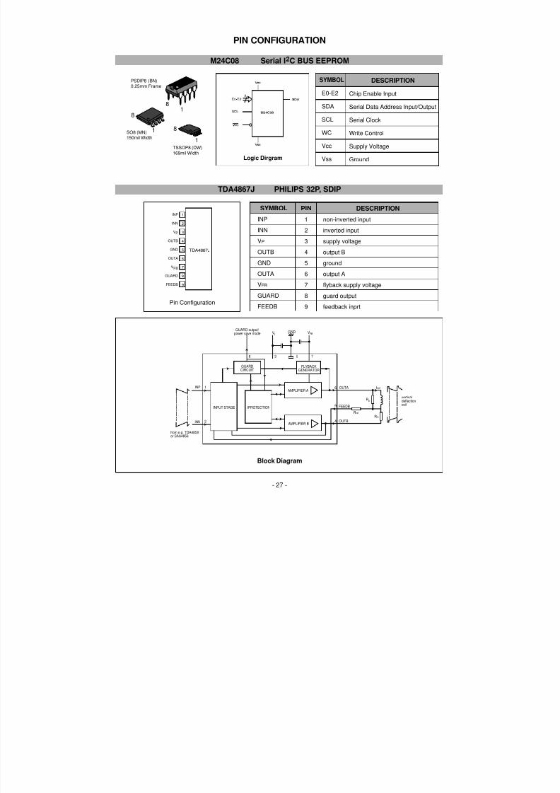
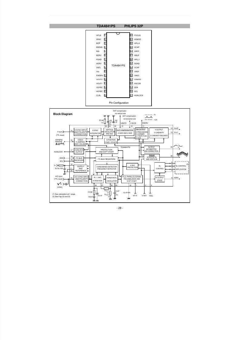
PIN CONFIGURATION
- 27 -
M24C08 Serial I 2C BUS EEPROM
SYMBOL
E0-E2
SDA
SCL
WC
Vcc
Vss
DESCRIPTION
Chip Enable Input
Serial Data Address Input/Output
Serial Clock
Write Control
Supply Voltage
Ground
1
PSDIP8 (BN)0.25mm Frame
8
1
1SO8 (MN)150mil Width
TSSOP8 (DW)169mil Width
8
8
Logic Dirgram
TDA4867J PHILIPS 32P, SDIP
AMPLIFIER A
FLYBACKGENERATOR
GUARDCIRCUIT
INPUT STAGE
from e.g TDA485Xor SAA4856
INP
INN
IPROTECTION
AMPLIFIER B4
9
6
8
1
2
3 5 7
OUTA
GUARO output/ power save mode GND
FEEDB
OUTB
verticaldeflectioncoil
Rp
Vp VFB
Rm
Rref
Idefl
Block Diagram
SYMBOL
INP
INN
VP
OUTB
GND
OUTA
VFB
GUARD
FEEDB
DESCRIPTION
non-inverted input
inverted input
supply voltage
output B
ground
output A
flyback supply voltage
guard output
feedback inprt
PIN
1
2
3
4
5
6
7
8
9
INP
INN
VP
OUTB
GND
OUTA
VFB
GUARD
FEEDB
1
2
3
4
5
6
7
8
9
TDA4867J
Pin Configuration
8/13/2019 (500g.pdf
http://slidepdf.com/reader/full/500gpdf 30/33
- 28 -
TDA4841PS PHLIPS 32P
1
2
3
4
5
6
7
8
9
10
11
12
1314
15
16
32
31
30
29
28
27
26
25
24
23
22
21
2019
18
17
FOCUS
HSMOD
HPLL2
HCAP
HREF
HBUF
HPLL1
SGND
VCAP
VREF
VAGC
VSMOD
ASCORSDA
SCL
HUNLOCK
HFLB
XRAY
BOP
BSENS
BIN
BDRV
PGND
HDRV
XSEL
Vcc
EWDRV
VOUT2
VOUT1VSYNC
HSYBC
CLBL
TDA4841PS
Pin Configuration
V-sync
(TTL level)
(TTL level)
(video)
15
25
10
18
192
17
16
14
7
H/C-SYNC INPUTAND POLARITYCORRECTION
(1) See calculation of f range.(2) See Figs 22 and 23.
SUPPLYAND
REFERENCE
HUNLOCKOUTPUT
VIDEOCLAMPING
AND V-BLANK
V-SYNC INPUTAND POLARITYCORRECTION
V-SYNC
INTEGRATOR
VERTICALOSCILLATOR
AND AGC
EHT COMPENSATION
H-SIZE AND V-SIZE
EW-OUTPUT V-OUTPUT
V-LINEARITY
V-LINEARITY BALANCE
H-PINCUSHIONH-CORNERH-TRAPEZIUMH-SIZE
OUTPUTASYMMETRIC
EW-CORRECTION
FOCUSHORIZONTAL
AND VERTICAL
B+
CONTROL
B+ CONTROL
APPLICATION
H-OUTPUT
STAGE
X-RAY
PROTECTION
PLL2, PARALLELOGRAM,PIN UNBALANCE AND
SOFT START
V-POSITIONV-SIZE, VOVSCN
TDA4841PS
I C-BUSRECEIVER
2I C-BUS REGISTERS
HUNLOCK
SDA
SCL
9.2 to 16V
H/C-sync
V+
clampingblanking
PROTECTIONAND SOFT START
COINCIDENCE DETECTORFREQUENCY DETECTOR
PLL1 AND
H-POSITION
HORIZONTAL
OSCILLATOR
12
13
Vout2
Vout1
20 or
32
8
9
XSELX-RAYHFLB
213029
122%
1%
nF10nF
8.2
3.3
nF100nF
282726
(1)RHBUF
RHREF
64
35
(2)
HDRV
23 24 22 21
VSMOD HSMOD
31 11
7V
1.2V221%
5%
100 150nF nF
EHT compensaton
EHT compensationvia vertical size
via horizontal size
EWDRV
H
Block Diagram
8/13/2019 (500g.pdf
http://slidepdf.com/reader/full/500gpdf 31/33
- 29 -
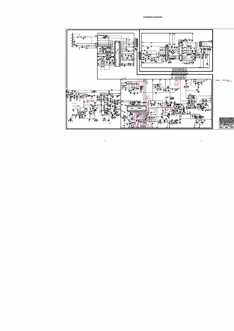
SCHEMATIC DIAGRAM
8/13/2019 (500g.pdf
http://slidepdf.com/reader/full/500gpdf 32/33
- 31 -
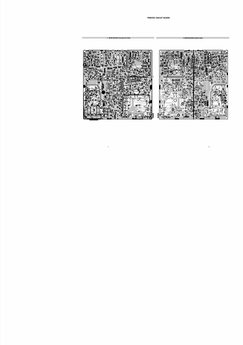
PRINTED CIRCUIT BOARD
1. MAIN BOARD (Component Side) 2. MAIN BOARD (Sold
8/13/2019 (500g.pdf
http://slidepdf.com/reader/full/500gpdf 33/33
Oct. 2003P/NO : 3828TSL092F Printed in Korea


