Embed Size (px)
Citation preview
This is information on a product in full production.
October 2015 DocID028544 Rev 1 1/101
VB6955CM
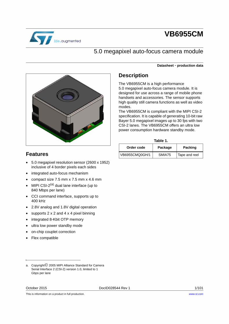
5.0 megapixel auto-focus camera module
Datasheet - production data
Features
• 5.0 megapixel resolution sensor (2600 x 1952) inclusive of 4 border pixels each sides
• integrated auto-focus mechanism
• compact size 7.5 mm x 7.5 mm x 4.6 mm
• MIPI CSI-2(a) dual lane interface (up to 840 Mbps per lane)
• CCI command interface, supports up to 400 kHz
• 2.8V analog and 1.8V digital operation
• supports 2 x 2 and 4 x 4 pixel binning
• integrated 8-Kbit OTP memory
• ultra low power standby mode
• on-chip couplet correction
• Flex compatible
Description
The VB6955CM is a high performance 5.0 megapixel auto-focus camera module. It is designed for use across a range of mobile phone handsets and accessories. The sensor supports high quality still camera functions as well as video modes. The VB6955CM is compliant with the MIPI CSI-2 specification. It is capable of generating 10-bit raw Bayer 5.0 megapixel images up to 30 fps with two CSI-2 lanes. The VB6955CM offers an ultra low power consumption hardware standby mode.
a. Copyright© 2005 MIPI Alliance Standard for Camera Serial Interface 2 (CSI-2) version 1.0, limited to 1 Gbps per lane
Table 1.
Order code Package Packing
VB6955CMQ0GH/1 SMIA75 Tape and reel
www.st.com
Contents VB6955CM
2/101 DocID028544 Rev 1
Contents
1 Overview . . . . . . . . . . . . . . . . . . . . . . . . . . . . . . . . . . . . . . . . . . . . . . . . . . 9
1.1 VB6955CM use in system with software image processing . . . . . . . . . . . 10
1.2 Reference documents . . . . . . . . . . . . . . . . . . . . . . . . . . . . . . . . . . . . . . . 10
2 Device pinout . . . . . . . . . . . . . . . . . . . . . . . . . . . . . . . . . . . . . . . . . . . . . . 11
3 Functional description . . . . . . . . . . . . . . . . . . . . . . . . . . . . . . . . . . . . . . 13
3.1 External clock . . . . . . . . . . . . . . . . . . . . . . . . . . . . . . . . . . . . . . . . . . . . . . 13
3.1.1 Clock input type . . . . . . . . . . . . . . . . . . . . . . . . . . . . . . . . . . . . . . . . . . . 13
3.1.2 PLL and clock input . . . . . . . . . . . . . . . . . . . . . . . . . . . . . . . . . . . . . . . . 13
3.2 Device operating modes . . . . . . . . . . . . . . . . . . . . . . . . . . . . . . . . . . . . . . 14
3.2.1 Power-up procedure . . . . . . . . . . . . . . . . . . . . . . . . . . . . . . . . . . . . . . . 15
3.2.2 Power-down procedure . . . . . . . . . . . . . . . . . . . . . . . . . . . . . . . . . . . . . 18
3.2.3 Internal power-on reset (POR) . . . . . . . . . . . . . . . . . . . . . . . . . . . . . . . . 20
3.2.4 Power off . . . . . . . . . . . . . . . . . . . . . . . . . . . . . . . . . . . . . . . . . . . . . . . . 21
3.2.5 Hardware standby . . . . . . . . . . . . . . . . . . . . . . . . . . . . . . . . . . . . . . . . . 21
3.2.6 Software standby . . . . . . . . . . . . . . . . . . . . . . . . . . . . . . . . . . . . . . . . . . 21
3.2.7 Streaming . . . . . . . . . . . . . . . . . . . . . . . . . . . . . . . . . . . . . . . . . . . . . . . . 21
3.2.8 Fast standby mode . . . . . . . . . . . . . . . . . . . . . . . . . . . . . . . . . . . . . . . . 22
4 Camera control interface (CCI) . . . . . . . . . . . . . . . . . . . . . . . . . . . . . . . 23
4.1 Valid register data types . . . . . . . . . . . . . . . . . . . . . . . . . . . . . . . . . . . . . . 23
4.2 Register map . . . . . . . . . . . . . . . . . . . . . . . . . . . . . . . . . . . . . . . . . . . . . . 24
4.2.1 Status registers [0x0000 to 0x001f] . . . . . . . . . . . . . . . . . . . . . . . . . . . . 24
4.2.2 Frame format description registers [0x0040 to 0x0049] . . . . . . . . . . . . 26
4.2.3 Analogue gain description registers [0x0080 to 0x0093] . . . . . . . . . . . . 26
4.2.4 Data format description registers [0x00c0 to 0x00c9] . . . . . . . . . . . . . . 27
4.2.5 Setup registers [0x0100 to 0x0137] . . . . . . . . . . . . . . . . . . . . . . . . . . . . 28
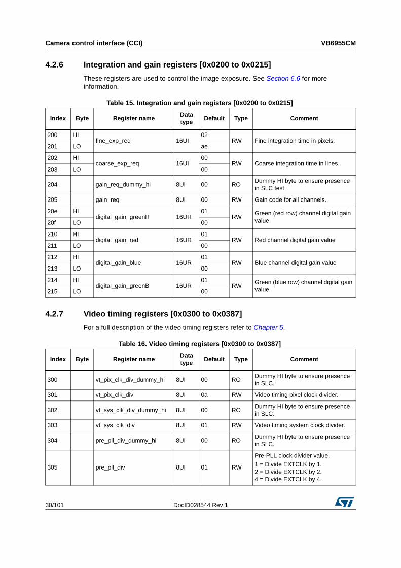
4.2.6 Integration and gain registers [0x0200 to 0x0215] . . . . . . . . . . . . . . . . . 30
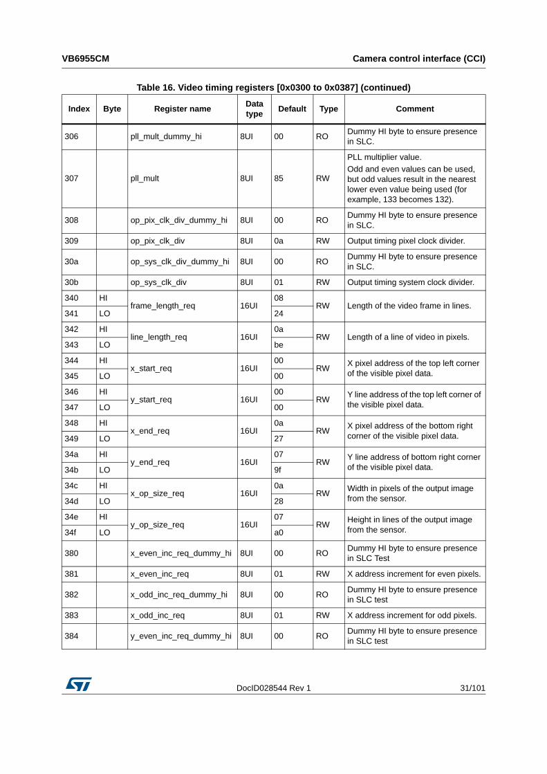
4.2.7 Video timing registers [0x0300 to 0x0387] . . . . . . . . . . . . . . . . . . . . . . . 30
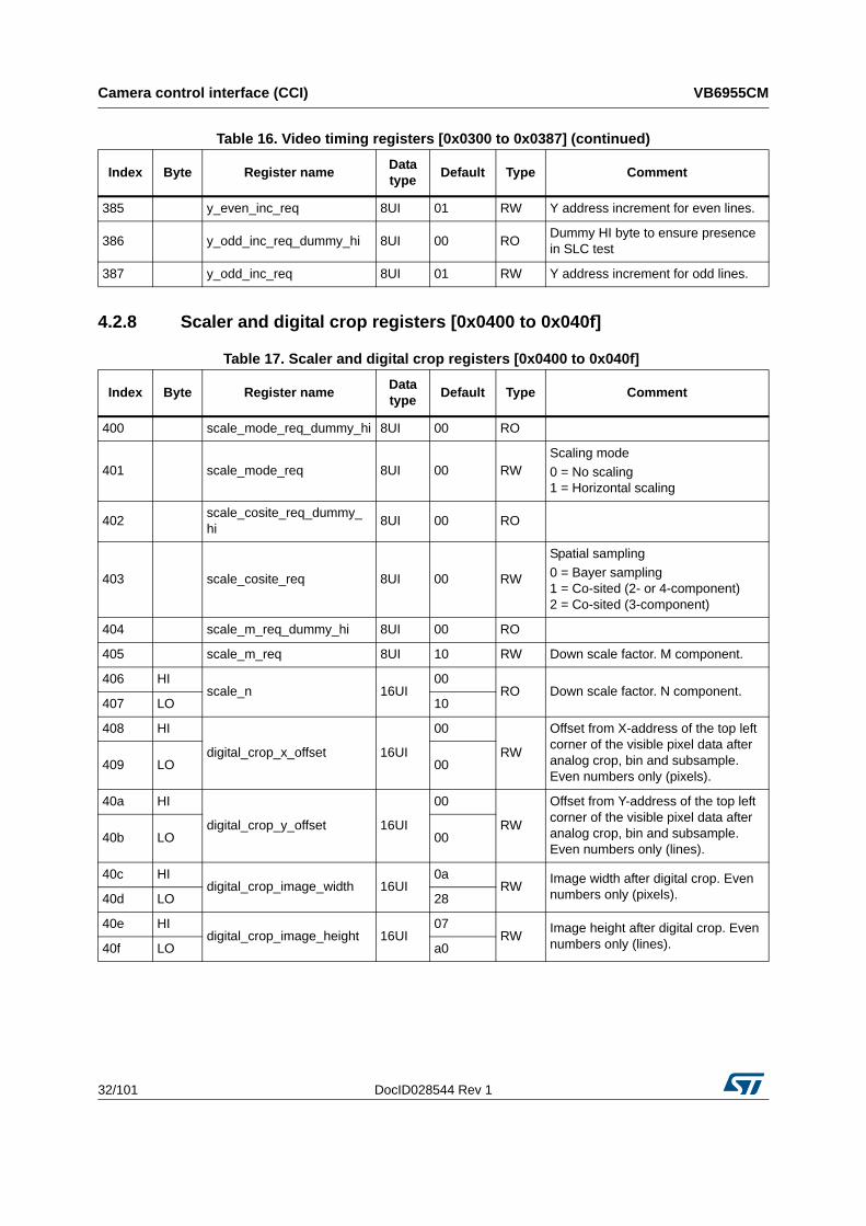
4.2.8 Scaler and digital crop registers [0x0400 to 0x040f] . . . . . . . . . . . . . . . 32
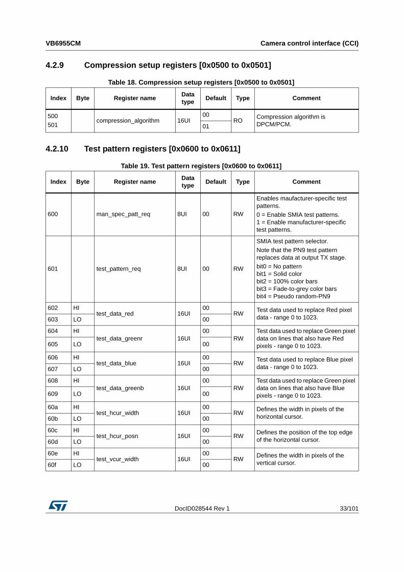
4.2.9 Compression setup registers [0x0500 to 0x0501] . . . . . . . . . . . . . . . . . 33
4.2.10 Test pattern registers [0x0600 to 0x0611] . . . . . . . . . . . . . . . . . . . . . . . 33
4.2.11 CSI2 registers [0x808] . . . . . . . . . . . . . . . . . . . . . . . . . . . . . . . . . . . . . . 34
DocID028544 Rev 1 3/101
VB6955CM Contents
5
4.2.12 DPHY registers [0x820 to 0x823] . . . . . . . . . . . . . . . . . . . . . . . . . . . . . 34
4.2.13 Binning registers [0x900 to 0x902] . . . . . . . . . . . . . . . . . . . . . . . . . . . . 35
4.2.14 Data transfer registers [0x0a00 to 0x0a43] . . . . . . . . . . . . . . . . . . . . . . 35
4.2.15 Ideal raw registers [0x0b04 to 0x0b05] . . . . . . . . . . . . . . . . . . . . . . . . . 36
4.2.16 Flash registers [0x0c12 to 0x0c2a] . . . . . . . . . . . . . . . . . . . . . . . . . . . . 36
4.2.17 Sensor - high level auto focus registers [0x0d80 to 0x0d89] . . . . . . . . . 37
4.2.18 Bracketing LUT registers [0x0e00 to 0x0e55] . . . . . . . . . . . . . . . . . . . . 38
4.2.19 Integration and gain limit registers [0x1000 to 0x1089] . . . . . . . . . . . . . 40
4.2.20 Video timing limit registers [0x1100 to 0x11c7] . . . . . . . . . . . . . . . . . . . 41
4.2.21 Scaling limit registers [0x1200 to 0x120f] . . . . . . . . . . . . . . . . . . . . . . . 45
4.2.22 Compression capability registers [0x1300 to 0x1301] . . . . . . . . . . . . . . 45
4.2.23 Derate capability registers [0x1500 to 0x1502] . . . . . . . . . . . . . . . . . . . 45
4.2.24 DPHY capability registers [0x1600 to 0x1604] . . . . . . . . . . . . . . . . . . . 46
4.2.25 Bitrate limit registers [0x1608 to 0x1617] . . . . . . . . . . . . . . . . . . . . . . . . 46
4.2.26 Binning capability registers [0x1700 to 0x1714] . . . . . . . . . . . . . . . . . . 47
4.2.27 Data transfer capability registers [0x1800] . . . . . . . . . . . . . . . . . . . . . . . 47
4.2.28 Ideal raw capability registers [0x1900 to 0x1907] . . . . . . . . . . . . . . . . . 48
4.2.29 EDOF capability registers [0x1980 to 0x19c5] . . . . . . . . . . . . . . . . . . . . 48
4.2.30 Timer capability registers [0x1a00 to 0x1a02] . . . . . . . . . . . . . . . . . . . . 48
4.2.31 Mechanical shutter capability registers [0x1b00 to 0x1b04] . . . . . . . . . 49
4.2.32 Static autofocus actuator capability registers [0x1b40 to 0x1b45] . . . . . 49
4.2.33 Bracketing LUT capability registers [0x1c00 to 0x1c02] . . . . . . . . . . . . 49
4.2.34 Manufacturer specific registers [0x6006 to 0x6008] . . . . . . . . . . . . . . . 50
5 Video data interface . . . . . . . . . . . . . . . . . . . . . . . . . . . . . . . . . . . . . . . . 51
5.1 Frame format . . . . . . . . . . . . . . . . . . . . . . . . . . . . . . . . . . . . . . . . . . . . . . 52
6 Video timing . . . . . . . . . . . . . . . . . . . . . . . . . . . . . . . . . . . . . . . . . . . . . . . 55
6.1 Output size . . . . . . . . . . . . . . . . . . . . . . . . . . . . . . . . . . . . . . . . . . . . . . . . 55
6.1.1 Analog crop . . . . . . . . . . . . . . . . . . . . . . . . . . . . . . . . . . . . . . . . . . . . . . 56
6.1.2 Subsampling . . . . . . . . . . . . . . . . . . . . . . . . . . . . . . . . . . . . . . . . . . . . . 57
6.1.3 Binning . . . . . . . . . . . . . . . . . . . . . . . . . . . . . . . . . . . . . . . . . . . . . . . . . . 58
6.1.4 Digital crop . . . . . . . . . . . . . . . . . . . . . . . . . . . . . . . . . . . . . . . . . . . . . . . 58
6.1.5 Scaling . . . . . . . . . . . . . . . . . . . . . . . . . . . . . . . . . . . . . . . . . . . . . . . . . . 59
6.1.6 Output crop . . . . . . . . . . . . . . . . . . . . . . . . . . . . . . . . . . . . . . . . . . . . . . 61
6.2 Video timing . . . . . . . . . . . . . . . . . . . . . . . . . . . . . . . . . . . . . . . . . . . . . . . 62
6.2.1 PLL block . . . . . . . . . . . . . . . . . . . . . . . . . . . . . . . . . . . . . . . . . . . . . . . . 62
Contents VB6955CM
4/101 DocID028544 Rev 1
6.2.2 Framerate . . . . . . . . . . . . . . . . . . . . . . . . . . . . . . . . . . . . . . . . . . . . . . . 63
6.2.3 Derating . . . . . . . . . . . . . . . . . . . . . . . . . . . . . . . . . . . . . . . . . . . . . . . . . 64
6.3 Image and video size capabilities . . . . . . . . . . . . . . . . . . . . . . . . . . . . . . . 66
6.4 Bayer pattern . . . . . . . . . . . . . . . . . . . . . . . . . . . . . . . . . . . . . . . . . . . . . . 66
6.5 Image compression . . . . . . . . . . . . . . . . . . . . . . . . . . . . . . . . . . . . . . . . . 68
6.6 Exposure and gain control . . . . . . . . . . . . . . . . . . . . . . . . . . . . . . . . . . . . 68
6.6.1 Analogue gain model . . . . . . . . . . . . . . . . . . . . . . . . . . . . . . . . . . . . . . . 69
6.6.2 Digital gain . . . . . . . . . . . . . . . . . . . . . . . . . . . . . . . . . . . . . . . . . . . . . . . 70
6.6.3 Integration and gain parameter re-timing . . . . . . . . . . . . . . . . . . . . . . . . 70
7 Electrical characteristics . . . . . . . . . . . . . . . . . . . . . . . . . . . . . . . . . . . . 71
7.1 Absolute maximum ratings . . . . . . . . . . . . . . . . . . . . . . . . . . . . . . . . . . . . 71
7.2 Operating conditions . . . . . . . . . . . . . . . . . . . . . . . . . . . . . . . . . . . . . . . . 72
7.3 DC electrical characteristics . . . . . . . . . . . . . . . . . . . . . . . . . . . . . . . . . . . 72
7.3.1 Power supply - VDIG, VANA, VBAT . . . . . . . . . . . . . . . . . . . . . . . . . . . . 72
7.3.2 CCI interface . . . . . . . . . . . . . . . . . . . . . . . . . . . . . . . . . . . . . . . . . . . . . 73
7.4 AC electrical and timing characteristics . . . . . . . . . . . . . . . . . . . . . . . . . . 73
7.4.1 Power supply (peak current) - VDIG, VANA . . . . . . . . . . . . . . . . . . . . . . 73
7.4.2 System clock - EXTCLK . . . . . . . . . . . . . . . . . . . . . . . . . . . . . . . . . . . . 74
7.4.3 EXTCLK - timing characteristics . . . . . . . . . . . . . . . . . . . . . . . . . . . . . . 74
7.4.4 CCI interface - timing characteristics . . . . . . . . . . . . . . . . . . . . . . . . . . . 74
7.4.5 CSI interface - DATA+, DATA-, CLK+, CLK- . . . . . . . . . . . . . . . . . . . . . 75
8 Optical specification . . . . . . . . . . . . . . . . . . . . . . . . . . . . . . . . . . . . . . . . 76
8.1 Lens characteristics . . . . . . . . . . . . . . . . . . . . . . . . . . . . . . . . . . . . . . . . . 76
8.2 User precaution . . . . . . . . . . . . . . . . . . . . . . . . . . . . . . . . . . . . . . . . . . . . 76
9 Autofocus . . . . . . . . . . . . . . . . . . . . . . . . . . . . . . . . . . . . . . . . . . . . . . . . . 77
9.1 VCM actuator . . . . . . . . . . . . . . . . . . . . . . . . . . . . . . . . . . . . . . . . . . . . . . 77
9.2 VCM driver/DAC . . . . . . . . . . . . . . . . . . . . . . . . . . . . . . . . . . . . . . . . . . . . 78
9.2.1 VCM driver control . . . . . . . . . . . . . . . . . . . . . . . . . . . . . . . . . . . . . . . . . 78
9.2.2 VCM driver register access . . . . . . . . . . . . . . . . . . . . . . . . . . . . . . . . . . 78
9.3 Examples . . . . . . . . . . . . . . . . . . . . . . . . . . . . . . . . . . . . . . . . . . . . . . . . . 79
9.4 Specification . . . . . . . . . . . . . . . . . . . . . . . . . . . . . . . . . . . . . . . . . . . . . . . 79
10 Non-volatile memory (NVM) . . . . . . . . . . . . . . . . . . . . . . . . . . . . . . . . . . 83
DocID028544 Rev 1 5/101
VB6955CM Contents
5
11 Defect categorization . . . . . . . . . . . . . . . . . . . . . . . . . . . . . . . . . . . . . . . 84
11.1 Pixel defects . . . . . . . . . . . . . . . . . . . . . . . . . . . . . . . . . . . . . . . . . . . . . . . 84
11.1.1 Overview . . . . . . . . . . . . . . . . . . . . . . . . . . . . . . . . . . . . . . . . . . . . . . . . 84
11.1.2 Defect detection . . . . . . . . . . . . . . . . . . . . . . . . . . . . . . . . . . . . . . . . . . . 84
11.1.3 Defect categorisation: Single pixels . . . . . . . . . . . . . . . . . . . . . . . . . . . . 85
11.1.4 Defect categorisation: Couplets . . . . . . . . . . . . . . . . . . . . . . . . . . . . . . . 85
11.1.5 Defect categorisation: Clusters and blobs . . . . . . . . . . . . . . . . . . . . . . . 85
11.2 Blemishes . . . . . . . . . . . . . . . . . . . . . . . . . . . . . . . . . . . . . . . . . . . . . . . . . 86
11.2.1 Blemish overview . . . . . . . . . . . . . . . . . . . . . . . . . . . . . . . . . . . . . . . . . . 86
11.2.2 Blemish algorithm . . . . . . . . . . . . . . . . . . . . . . . . . . . . . . . . . . . . . . . . . 86
12 On-chip image optimization . . . . . . . . . . . . . . . . . . . . . . . . . . . . . . . . . . 89
12.1 Mapped couplet correction (Bruce filter) . . . . . . . . . . . . . . . . . . . . . . . . . 89
13 Mechanical . . . . . . . . . . . . . . . . . . . . . . . . . . . . . . . . . . . . . . . . . . . . . . . . 90
14 Application . . . . . . . . . . . . . . . . . . . . . . . . . . . . . . . . . . . . . . . . . . . . . . . . 96
14.1 Schematic . . . . . . . . . . . . . . . . . . . . . . . . . . . . . . . . . . . . . . . . . . . . . . . . . 96
15 Acronyms and abbreviations . . . . . . . . . . . . . . . . . . . . . . . . . . . . . . . . . 97
16 ECOPACK® . . . . . . . . . . . . . . . . . . . . . . . . . . . . . . . . . . . . . . . . . . . . . . . . . . . . . . . . . . . . 99
17 Revision history . . . . . . . . . . . . . . . . . . . . . . . . . . . . . . . . . . . . . . . . . . 100
List of tables VB6955CM
6/101 DocID028544 Rev 1
List of tables
Table 1. . . . . . . . . . . . . . . . . . . . . . . . . . . . . . . . . . . . . . . . . . . . . . . . . . . . . . . . . . . . . . . . . . . . . . . . 1Table 2. Technical specification . . . . . . . . . . . . . . . . . . . . . . . . . . . . . . . . . . . . . . . . . . . . . . . . . . . . . 9Table 3. Reference documents. . . . . . . . . . . . . . . . . . . . . . . . . . . . . . . . . . . . . . . . . . . . . . . . . . . . . 10Table 4. Pin description . . . . . . . . . . . . . . . . . . . . . . . . . . . . . . . . . . . . . . . . . . . . . . . . . . . . . . . . . . 11Table 5. System input clock frequency range. . . . . . . . . . . . . . . . . . . . . . . . . . . . . . . . . . . . . . . . . . 13Table 6. Power-up sequence timing constraints . . . . . . . . . . . . . . . . . . . . . . . . . . . . . . . . . . . . . . . . 15Table 7. Power-down sequence timing constraints for CSI2 communications . . . . . . . . . . . . . . . . . 18Table 8. POR cell characteristics . . . . . . . . . . . . . . . . . . . . . . . . . . . . . . . . . . . . . . . . . . . . . . . . . . . 21Table 9. Valid register data types . . . . . . . . . . . . . . . . . . . . . . . . . . . . . . . . . . . . . . . . . . . . . . . . . . . 23Table 10. Status registers [0x0000 to 0x001f] . . . . . . . . . . . . . . . . . . . . . . . . . . . . . . . . . . . . . . . . . . 24Table 11. Frame format description registers [0x0040 to 0x0049] . . . . . . . . . . . . . . . . . . . . . . . . . . . 26Table 12. Analogue gain description [0x0080 to 0x0093] . . . . . . . . . . . . . . . . . . . . . . . . . . . . . . . . . . 26Table 13. Data format description registers [0x00c0 to 0x00c9]. . . . . . . . . . . . . . . . . . . . . . . . . . . . . 27Table 14. Setup registers [0x0100 to 0x0137] . . . . . . . . . . . . . . . . . . . . . . . . . . . . . . . . . . . . . . . . . . 28Table 15. Integration and gain registers [0x0200 to 0x0215] . . . . . . . . . . . . . . . . . . . . . . . . . . . . . . . 30Table 16. Video timing registers [0x0300 to 0x0387] . . . . . . . . . . . . . . . . . . . . . . . . . . . . . . . . . . . . . 30Table 17. Scaler and digital crop registers [0x0400 to 0x040f] . . . . . . . . . . . . . . . . . . . . . . . . . . . . . . 32Table 18. Compression setup registers [0x0500 to 0x0501] . . . . . . . . . . . . . . . . . . . . . . . . . . . . . . . 33Table 19. Test pattern registers [0x0600 to 0x0611] . . . . . . . . . . . . . . . . . . . . . . . . . . . . . . . . . . . . . 33Table 20. CSI2 registers [0x808] . . . . . . . . . . . . . . . . . . . . . . . . . . . . . . . . . . . . . . . . . . . . . . . . . . . . 34Table 21. DPHY registers [0x820 to 0x823] . . . . . . . . . . . . . . . . . . . . . . . . . . . . . . . . . . . . . . . . . . . . 34Table 22. Binning registers [0x900 to 0x902] . . . . . . . . . . . . . . . . . . . . . . . . . . . . . . . . . . . . . . . . . . . 35Table 23. Data transfer registers [0x0a00 to 0x0a43]. . . . . . . . . . . . . . . . . . . . . . . . . . . . . . . . . . . . . 35Table 24. Ideal raw registers [0x0b04 to 0x0b05] . . . . . . . . . . . . . . . . . . . . . . . . . . . . . . . . . . . . . . . . 36Table 25. Flash registers [0x0c12 to 0x0c2a] . . . . . . . . . . . . . . . . . . . . . . . . . . . . . . . . . . . . . . . . . . . 36Table 26. Sensor - high level auto focus registers [0x0d80 to 0x0d89] . . . . . . . . . . . . . . . . . . . . . . . 37Table 27. Bracketing LUT registers [0x0e00 to 0x0e55]. . . . . . . . . . . . . . . . . . . . . . . . . . . . . . . . . . . 38Table 28. Integration and gain limit registers [0x1000 to 0x1089] . . . . . . . . . . . . . . . . . . . . . . . . . . . 40Table 29. Video timing limit registers [0x1100 to 0x11c7] . . . . . . . . . . . . . . . . . . . . . . . . . . . . . . . . . 41Table 30. Scaling limit registers [0x1200 to 0x120f] . . . . . . . . . . . . . . . . . . . . . . . . . . . . . . . . . . . . . . 45Table 31. Compression capability registers [0x1300 to 0x1301] . . . . . . . . . . . . . . . . . . . . . . . . . . . . 45Table 32. Derate capability registers [0x1500 to 0x1502]. . . . . . . . . . . . . . . . . . . . . . . . . . . . . . . . . . 45Table 33. DPHY capability registers [0x1600 to 0x1604] . . . . . . . . . . . . . . . . . . . . . . . . . . . . . . . . . . 46Table 34. Bitrate limit registers [0x1608 to 0x1617] . . . . . . . . . . . . . . . . . . . . . . . . . . . . . . . . . . . . . . 46Table 35. Binning capability registers [0x1700 to 0x1714] . . . . . . . . . . . . . . . . . . . . . . . . . . . . . . . . . 47Table 36. Data transfer capability registers [0x1800] . . . . . . . . . . . . . . . . . . . . . . . . . . . . . . . . . . . . . 47Table 37. Ideal raw capability registers [0x1900 to 0x1907] . . . . . . . . . . . . . . . . . . . . . . . . . . . . . . . . 48Table 38. EDOF capability registers [0x1980 to 0x19c5] . . . . . . . . . . . . . . . . . . . . . . . . . . . . . . . . . . 48Table 39. Timer capability registers [0x1a00 to 0x1a02] . . . . . . . . . . . . . . . . . . . . . . . . . . . . . . . . . . 48Table 40. Mechanical shutter capability registers [0x1b00 to 0x1b04] . . . . . . . . . . . . . . . . . . . . . . . . 49Table 41. Static autofocus actuator capability registers [0x1b40 to 0x1b45] . . . . . . . . . . . . . . . . . . . 49Table 42. Bracketing LUT capability registers [0x1c00 to 0x1c02] . . . . . . . . . . . . . . . . . . . . . . . . . . . 49Table 43. Manufacturer specific registers [0x6006 to 0x6008] . . . . . . . . . . . . . . . . . . . . . . . . . . . . . . 50Table 44. External clock frequency examples - 5.0 Mpixel Raw10 30 fps (CSI-2 dual lane) . . . . . . . 63Table 45. External clock frequency examples - 5.0 Mpixel Raw10 15 fps (CSI-2 single lane) . . . . . . 63Table 46. Examples of video mode capabilities . . . . . . . . . . . . . . . . . . . . . . . . . . . . . . . . . . . . . . . . . 66Table 47. Analogue gain control . . . . . . . . . . . . . . . . . . . . . . . . . . . . . . . . . . . . . . . . . . . . . . . . . . . . . 69Table 48. Absolute maximum ratings . . . . . . . . . . . . . . . . . . . . . . . . . . . . . . . . . . . . . . . . . . . . . . . . . 71
DocID028544 Rev 1 7/101
VB6955CM List of tables
7
Table 49. Operating conditions. . . . . . . . . . . . . . . . . . . . . . . . . . . . . . . . . . . . . . . . . . . . . . . . . . . . . . 72Table 50. Power supply - VDIG, VANA, VBAT . . . . . . . . . . . . . . . . . . . . . . . . . . . . . . . . . . . . . . . . . . 72Table 51. CCI interface. . . . . . . . . . . . . . . . . . . . . . . . . . . . . . . . . . . . . . . . . . . . . . . . . . . . . . . . . . . . 73Table 52. In-rush current - VDIG, VANA (CSI-2) . . . . . . . . . . . . . . . . . . . . . . . . . . . . . . . . . . . . . . . . 73Table 53. System clock. . . . . . . . . . . . . . . . . . . . . . . . . . . . . . . . . . . . . . . . . . . . . . . . . . . . . . . . . . . . 74Table 54. External clock timing characteristics . . . . . . . . . . . . . . . . . . . . . . . . . . . . . . . . . . . . . . . . . . 74Table 55. CCI interface timing characteristics . . . . . . . . . . . . . . . . . . . . . . . . . . . . . . . . . . . . . . . . . . 74Table 56. CSI interface - DATA+, DATA-, CLK+, CLK- characteristics . . . . . . . . . . . . . . . . . . . . . . . 75Table 57. Lens design characteristics for first source lens supplier . . . . . . . . . . . . . . . . . . . . . . . . . . 76Table 58. Autofocus specification - Type M . . . . . . . . . . . . . . . . . . . . . . . . . . . . . . . . . . . . . . . . . . . . 79Table 59. Autofocus specification - Type L. . . . . . . . . . . . . . . . . . . . . . . . . . . . . . . . . . . . . . . . . . . . . 81Table 60. NVM register summary . . . . . . . . . . . . . . . . . . . . . . . . . . . . . . . . . . . . . . . . . . . . . . . . . . . . 83Table 61. Pixel defect specification . . . . . . . . . . . . . . . . . . . . . . . . . . . . . . . . . . . . . . . . . . . . . . . . . . 84Table 62. Image settings . . . . . . . . . . . . . . . . . . . . . . . . . . . . . . . . . . . . . . . . . . . . . . . . . . . . . . . . . . 84Table 63. Acronyms and abbreviations . . . . . . . . . . . . . . . . . . . . . . . . . . . . . . . . . . . . . . . . . . . . . . . 97Table 64. Document revision history . . . . . . . . . . . . . . . . . . . . . . . . . . . . . . . . . . . . . . . . . . . . . . . . 100
List of figures VB6955CM
8/101 DocID028544 Rev 1
List of figures
Figure 1. VB6955CM in system with software image processing . . . . . . . . . . . . . . . . . . . . . . . . . . . 10Figure 2. VB6955CM module pinout (viewed from bottom of camera module) . . . . . . . . . . . . . . . . . 11Figure 3. Clock input types . . . . . . . . . . . . . . . . . . . . . . . . . . . . . . . . . . . . . . . . . . . . . . . . . . . . . . . . 13Figure 4. System state diagram . . . . . . . . . . . . . . . . . . . . . . . . . . . . . . . . . . . . . . . . . . . . . . . . . . . . . 14Figure 5. VB6955CM power-up sequence for CCP2 mode . . . . . . . . . . . . . . . . . . . . . . . . . . . . . . . . 16Figure 6. VB6955CM power-up sequence for CSI-2 mode . . . . . . . . . . . . . . . . . . . . . . . . . . . . . . . . 17Figure 7. VB6955CM power-down sequence for CSI-2 mode. . . . . . . . . . . . . . . . . . . . . . . . . . . . . . 19Figure 8. POR timing . . . . . . . . . . . . . . . . . . . . . . . . . . . . . . . . . . . . . . . . . . . . . . . . . . . . . . . . . . . . . 20Figure 9. VB6955CM CCP2 frame format . . . . . . . . . . . . . . . . . . . . . . . . . . . . . . . . . . . . . . . . . . . . . 52Figure 10. VB6955CM CSI-2 frame format . . . . . . . . . . . . . . . . . . . . . . . . . . . . . . . . . . . . . . . . . . . . . 53Figure 11. Data flow. . . . . . . . . . . . . . . . . . . . . . . . . . . . . . . . . . . . . . . . . . . . . . . . . . . . . . . . . . . . . . . 55Figure 12. Programmable addressable region of the pixel array . . . . . . . . . . . . . . . . . . . . . . . . . . . . . 56Figure 13. Subsample readout example . . . . . . . . . . . . . . . . . . . . . . . . . . . . . . . . . . . . . . . . . . . . . . . 57Figure 14. Digital crop . . . . . . . . . . . . . . . . . . . . . . . . . . . . . . . . . . . . . . . . . . . . . . . . . . . . . . . . . . . . . 58Figure 15. Scaling modes . . . . . . . . . . . . . . . . . . . . . . . . . . . . . . . . . . . . . . . . . . . . . . . . . . . . . . . . . . 59Figure 16. Scaler quality . . . . . . . . . . . . . . . . . . . . . . . . . . . . . . . . . . . . . . . . . . . . . . . . . . . . . . . . . . . 60Figure 17. Example image horizontal scaled by a downscale factor of 2 . . . . . . . . . . . . . . . . . . . . . . 60Figure 18. Output size within a CCP data frame . . . . . . . . . . . . . . . . . . . . . . . . . . . . . . . . . . . . . . . . . 61Figure 19. VB6955CM clock relationships . . . . . . . . . . . . . . . . . . . . . . . . . . . . . . . . . . . . . . . . . . . . . . 62Figure 20. Timing block diagram . . . . . . . . . . . . . . . . . . . . . . . . . . . . . . . . . . . . . . . . . . . . . . . . . . . . . 64Figure 21. SMIA output timing . . . . . . . . . . . . . . . . . . . . . . . . . . . . . . . . . . . . . . . . . . . . . . . . . . . . . . . 65Figure 22. Bayer pattern . . . . . . . . . . . . . . . . . . . . . . . . . . . . . . . . . . . . . . . . . . . . . . . . . . . . . . . . . . . 67Figure 23. Analogue gain register format. . . . . . . . . . . . . . . . . . . . . . . . . . . . . . . . . . . . . . . . . . . . . . . 69Figure 24. External clock timing. . . . . . . . . . . . . . . . . . . . . . . . . . . . . . . . . . . . . . . . . . . . . . . . . . . . . . 74Figure 25. CCI AC characteristics . . . . . . . . . . . . . . . . . . . . . . . . . . . . . . . . . . . . . . . . . . . . . . . . . . . . 75Figure 26. Host and VB6955CM module system overview . . . . . . . . . . . . . . . . . . . . . . . . . . . . . . . . . 77Figure 27. Typical plot of displacement versus DAC control . . . . . . . . . . . . . . . . . . . . . . . . . . . . . . . . 78Figure 28. Pixel numbering notation . . . . . . . . . . . . . . . . . . . . . . . . . . . . . . . . . . . . . . . . . . . . . . . . . . 85Figure 29. Single pixel fault . . . . . . . . . . . . . . . . . . . . . . . . . . . . . . . . . . . . . . . . . . . . . . . . . . . . . . . . . 85Figure 30. Couplet pixel fault . . . . . . . . . . . . . . . . . . . . . . . . . . . . . . . . . . . . . . . . . . . . . . . . . . . . . . . . 85Figure 31. Blemish convolution areas . . . . . . . . . . . . . . . . . . . . . . . . . . . . . . . . . . . . . . . . . . . . . . . . . 86Figure 32. Scan array for blemish . . . . . . . . . . . . . . . . . . . . . . . . . . . . . . . . . . . . . . . . . . . . . . . . . . . . 87Figure 33. Fail map . . . . . . . . . . . . . . . . . . . . . . . . . . . . . . . . . . . . . . . . . . . . . . . . . . . . . . . . . . . . . . . 87Figure 34. Contiguous pixel example. . . . . . . . . . . . . . . . . . . . . . . . . . . . . . . . . . . . . . . . . . . . . . . . . . 88Figure 35. VB6955CM exploded view . . . . . . . . . . . . . . . . . . . . . . . . . . . . . . . . . . . . . . . . . . . . . . . . . 90Figure 36. VB6955CM outline drawing in mm - sheet 1 of 6 . . . . . . . . . . . . . . . . . . . . . . . . . . . . . . . . 91Figure 37. VB6955CM outline drawing in mm - sheet 2 of 6 . . . . . . . . . . . . . . . . . . . . . . . . . . . . . . . . 92Figure 38. VB6955CM outline drawing in mm - sheet 3 of 6 . . . . . . . . . . . . . . . . . . . . . . . . . . . . . . . . 93Figure 39. VB6955CM outline drawing in mm - sheet 4 of 6 . . . . . . . . . . . . . . . . . . . . . . . . . . . . . . . . 93Figure 40. VB6955CM outline drawing in mm - sheet 5 of 6 . . . . . . . . . . . . . . . . . . . . . . . . . . . . . . . . 94Figure 41. VB6955CM outline drawing in mm - sheet 6 of 6 . . . . . . . . . . . . . . . . . . . . . . . . . . . . . . . . 95Figure 42. Mobile camera application . . . . . . . . . . . . . . . . . . . . . . . . . . . . . . . . . . . . . . . . . . . . . . . . . 96
DocID028544 Rev 1 9/101
VB6955CM Overview
22
1 Overview
The VB6955CM image sensor produces raw digital video data at up to 30 frames per second. The sensor supports horizontal flip and vertical mirroring. Output frequency can be derated as defined in the specification for power saving. Higher frame rate can be achieved through analog binning and subsampling modes.
The image data is digitized using an internal 10-bit column ADC. The resulting pixel data is output together with checksums and embedded codes for synchronization. The interface conforms to MIPI CSI-2 interface standards.
The sensor is fully configurable through a CCI serial interface. Both the CSI-2 and CCI interfaces are specified in a separate document: MIPI alliance standard for camera serial interface 2 (CSI-2).
Table 2. Technical specification
Feature Detail
Pixel resolution 2600x 1952 with border pixels
Sensor technology ST IMG140 FSI Gen2 based CMOS imaging process
Pixel size 1.4 µm x 1.4 µm
Analog gain + 24 dB
Digital gain + 6 dB
Dynamic range 60 dB
Signal to noise 36 dB (@ 100 lux)
Supply voltages
Analog: 2.6 to 2.9V
Digital: 1.7 to 1.9 V
VBAT: 2.5 to 4.8V
Typical power consumption 30 fps
130 mA (typical)
Operating temperature -30°C to +70°C
Storage temperature -40°C to +85°C
Average dark current (60C) 25 e/s
Shading (60C) 12 e/s
Overview VB6955CM
10/101 DocID028544 Rev 1
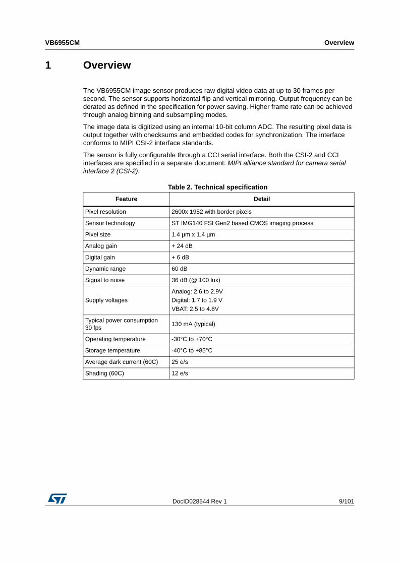
1.1 VB6955CM use in system with software image processing
The VB6955CM image sensor can be directly connected to a baseband or multimedia processor. The image processing is done in software or hardware within the baseband processor.
Figure 1. VB6955CM in system with software image processing
1.2 Reference documents
PixelarrayY
-de
c
Col ADC
Power ma
nag
em
ent
Video engine
CCI
Test ctrl
Sys ctrl
Clk mngt
PLL
Module
Mobile
baseband
processor
EXTCLK
CSI-2
Output data I/F
Derating
Video timing
CSI-2
Dark cal
Defect Corr.
Table 3. Reference documents
Title Date
MIPI Alliance Standard for Camera Serial Interface 2 (CSI-2) v1.0 29/11/2005
MIPI Alliance D-PHY Specification (v1.00.00) 14/05/2009
DocID028544 Rev 1 11/101
VB6955CM Device pinout
22
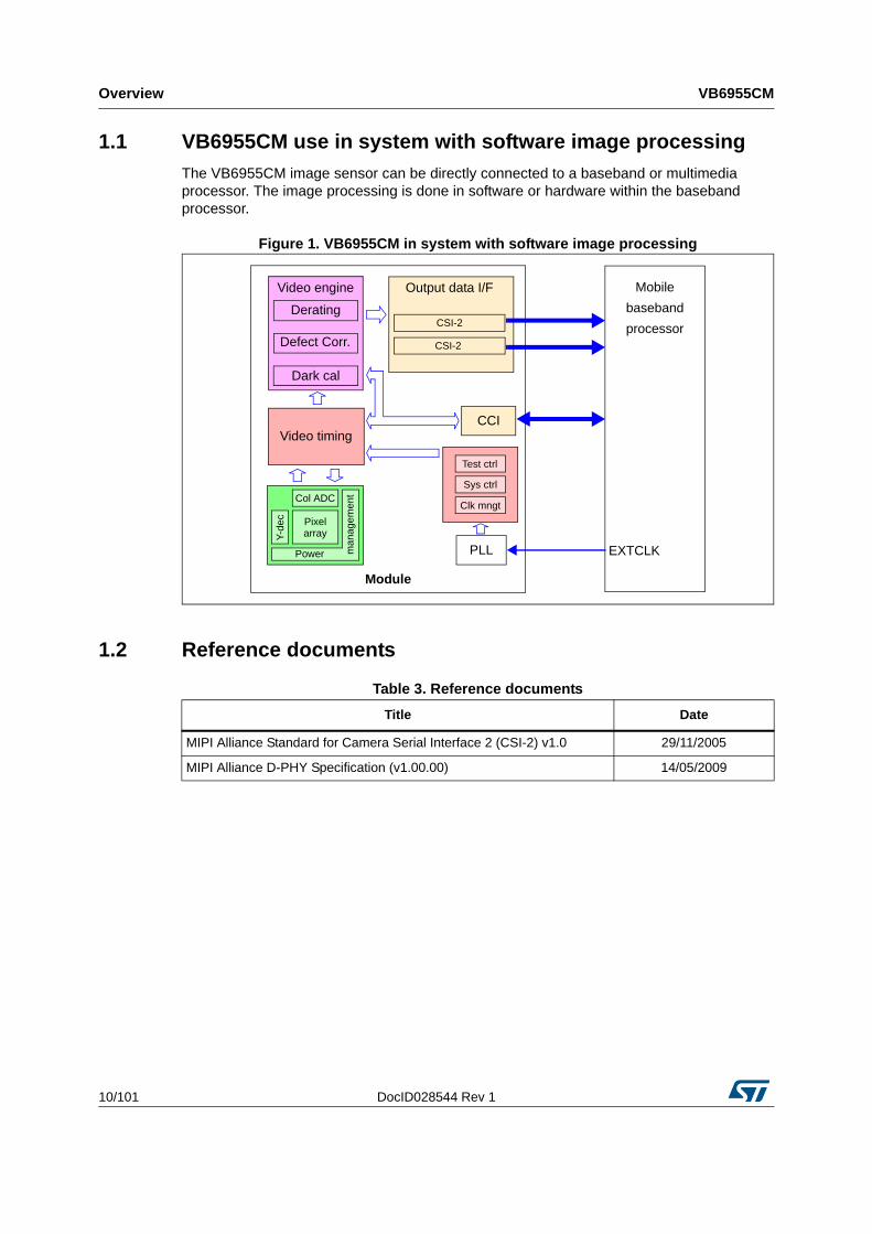
2 Device pinout
Figure 2 shows the position of the pins on the module and Table 4 provides the signal descriptions.
Figure 2. VB6955CM module pinout (viewed from bottom of camera module)
Table 4. Pin description
Pad number Pad name Description
Power supplies
3 VBAT VCM power
7, 11 DGND, AGND Digital and analog ground
8 VANA Analog power
14 VCM_GND VCM ground
1 VDIG Digital power
System
6 FSTROBE Flash strobe
5 EXTCLK System clock input
Control
4 SCL Serial communication clock
2 SDA Serial communication data
18
169
T1
Device pinout VB6955CM
12/101 DocID028544 Rev 1
Data
12 CLK-(1) Output qualifying clock
13 CLK+(1) Output qualifying clock
9 DATA1-(1) Serial output data
10 DATA1+(1) Serial output data
15 DATA2-(1)/ CCP DATA+ Serial output data
16 DATA2+(1)/ CCP DATA- Serial output data
ST test
T1 ST test pin Do not connect(2)
1. By default, the polarity of the CSI-2 data lanes and clock lanes are swapped. It is necessary to swap them by writing 0x02 to the registers 0x6006, 0x6007 and 0x6008. It is not possible to swap the CCP data lanes.
2. Test pin is not floating.
Table 4. Pin description (continued)
Pad number Pad name Description
DocID028544 Rev 1 13/101
VB6955CM Functional description
22
3 Functional description
3.1 External clock
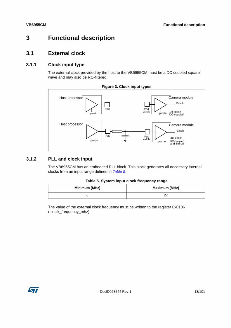
3.1.1 Clock input type
The external clock provided by the host to the VB6955CM must be a DC coupled square wave and may also be RC-filtered.
Figure 3. Clock input types
3.1.2 PLL and clock input
The VB6955CM has an embedded PLL block. This block generates all necessary internal clocks from an input range defined in Table 5.
The value of the external clock frequency must be written to the register 0x0136 (extclk_frequency_mhz).
Pad Pad
Extclk
extclk
Camera moduleHost processor
Pad Pad
Extclk
extclk
Camera moduleHost processor
1st optionDC-coupled
2nd optionDC-coupledand filtered
pwrdn
pwrdnpwrdn
pwrdn
Table 5. System input clock frequency range
Minimum (MHz) Maximum (MHz)
6 27
Functional description VB6955CM
14/101 DocID028544 Rev 1
3.2 Device operating modes
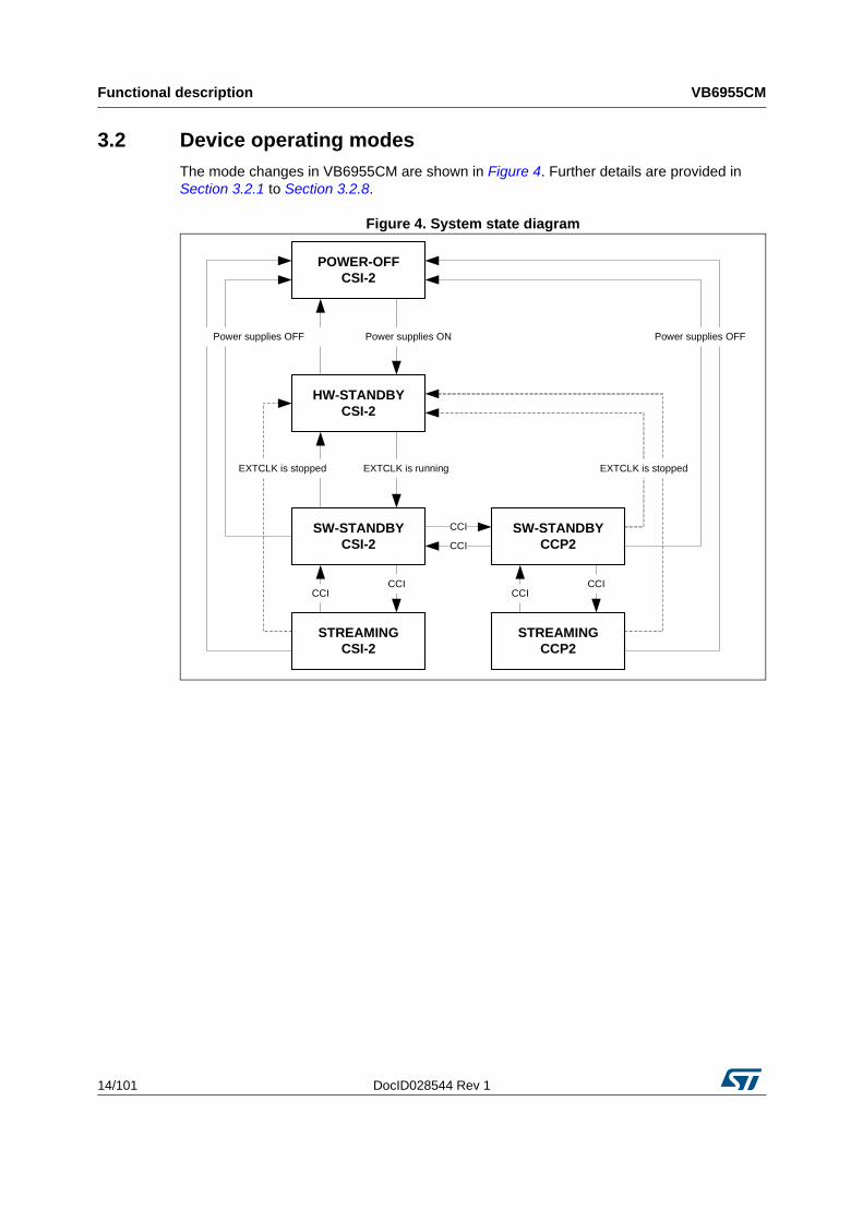
The mode changes in VB6955CM are shown in Figure 4. Further details are provided in Section 3.2.1 to Section 3.2.8.
Figure 4. System state diagram
STREAMINGCSI-2
SW-STANDBYCCP2
SW-STANDBYCSI-2
HW-STANDBYCSI-2
POWER-OFFCSI-2
STREAMINGCCP2
CCICCI
CCICCI
CCI
CCI
EXTCLK is runningEXTCLK is stopped
Power supplies ONPower supplies OFF
EXTCLK is stopped
Power supplies OFF
DocID028544 Rev 1 15/101
VB6955CM Functional description
22
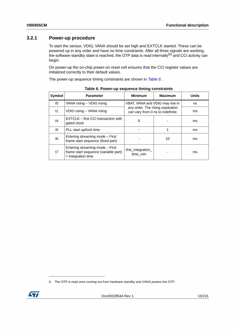
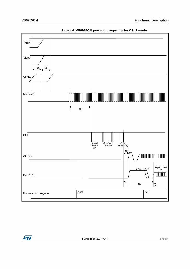
3.2.1 Power-up procedure
To start the sensor, VDIG, VANA should be set high and EXTCLK started. These can be powered up in any order and have no time constraints. After all three signals are working, the software standby state is reached, the OTP data is read internally(b) and CCI activity can begin.
On power-up the on-chip power-on reset cell ensures that the CCI register values are initialized correctly to their default values.
The power-up sequence timing constraints are shown in Table 6.
b. The OTP is read once coming out from hardware standby and VANA powers the OTP.
Table 6. Power-up sequence timing constraints
Symbol Parameter Minimum Maximum Units
t0 VANA rising – VDIG rising VBAT, VANA and VDIG may rise in any order. The rising separation can vary from 0 ns to indefinite.
ns
t1 VDIG rising – VANA rising ms
t4EXTCLK – first CCI transaction with gated clock
5 - ms
t5 PLL start up/lock time - 1 ms
t6Entering streaming mode – First frame start sequence (fixed part)
- 10 ms
t7Entering streaming mode – First frame start sequence (variable part) = Integration time
fine_integration_time_min
- ms
Functional description VB6955CM
16/101 DocID028544 Rev 1
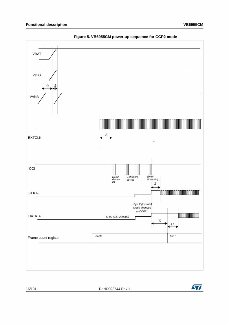
Figure 5. VB6955CM power-up sequence for CCP2 mode
t0 t1
t4
t5
t6
VDIG
VANA
EXTCLK
CCI
CLK+/-
DATA+/-
Frame count register
ReaddeviceID
Configure device
Enterstreaming
0xFF 0x01
t7
High Z (tri-state)
LP00 (CSI-2 mode)
Mode changed to CCP2
VBAT
DocID028544 Rev 1 17/101
VB6955CM Functional description
22
Figure 6. VB6955CM power-up sequence for CSI-2 mode
t6
CCI
CLK+/-
DATA+/-
Frame count register
Readdevice
ID
Configure device
Enterstreaming
0xFF 0x01
High-speedTX
t0 t1
VDIG
VANA
t4
EXTCLK
LP11 LP01
t5
t7
VBAT
Functional description VB6955CM
18/101 DocID028544 Rev 1
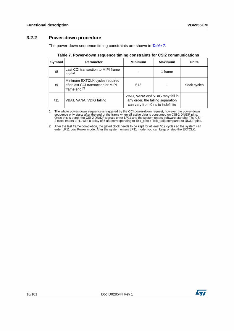
3.2.2 Power-down procedure
The power-down sequence timing constraints are shown in Table 7.
Table 7. Power-down sequence timing constraints for CSI2 communications
Symbol Parameter Minimum Maximum Units
t8Last CCI transaction to MIPI frame end(1)
1. The whole power-down sequence is triggered by the CCI power-down request, however the power-down sequence only starts after the end of the frame when all active data is consumed on CSI-2 DN/DP pins. Once this is done, the CSI-2 DN/DP signals enter LP11 and the system enters software standby. The CSI-2 clock enters LP11 with a delay of 5 us (corresponding to Tclk_post + Tclk_trail) compared to DN/DP pins.
- 1 frame
t9Minimum EXTCLK cycles required after last CCI transaction or MIPI frame end(2)
2. After the last frame completion, the gated clock needs to be kept for at least 512 cycles so the system can enter LP11 Low Power mode. After the system enters LP11 mode, you can keep or stop the EXTCLK.
512 - clock cycles
t11 VBAT, VANA, VDIG fallingVBAT, VANA and VDIG may fall in
any order, the falling separation can vary from 0 ns to indefinite
DocID028544 Rev 1 19/101
VB6955CM Functional description
22
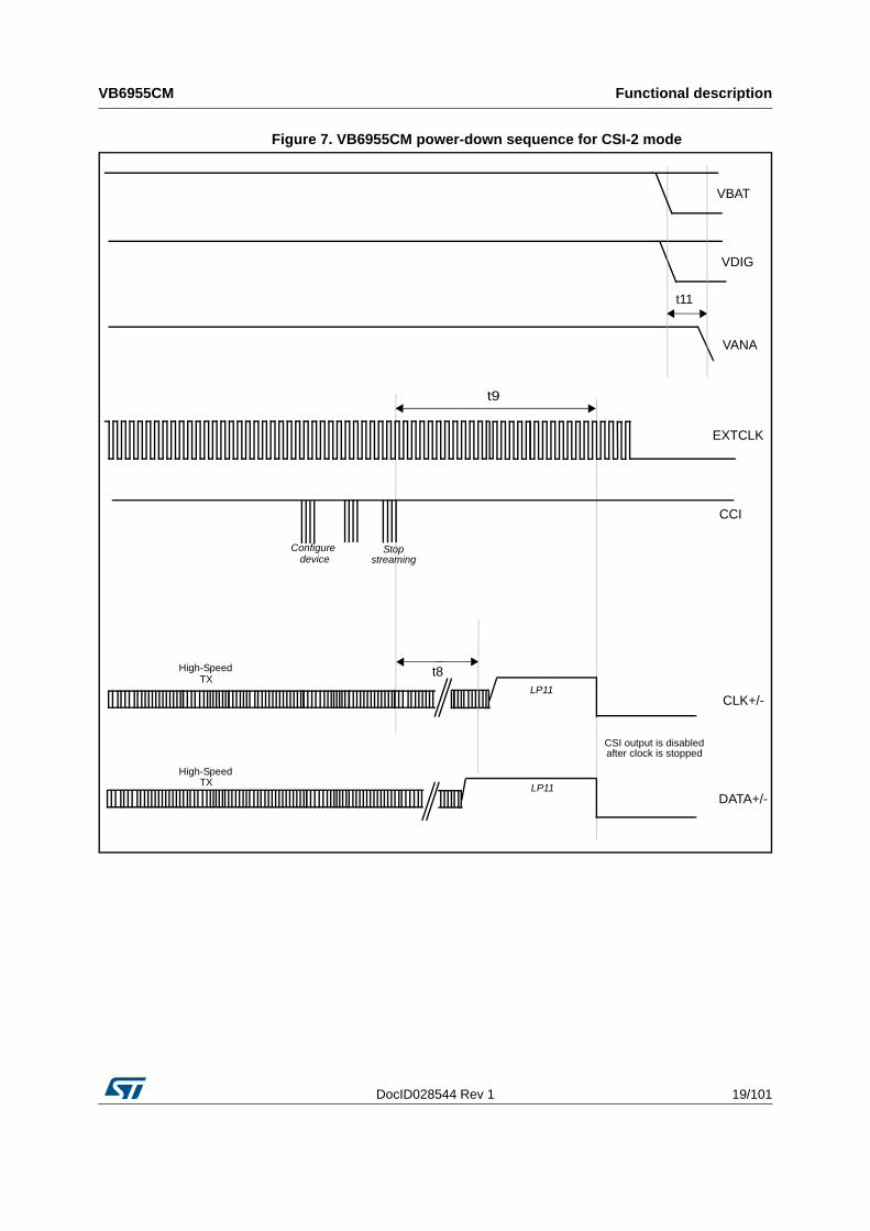
Figure 7. VB6955CM power-down sequence for CSI-2 mode
EXTCLK
CCI
CLK+/-
DATA+/-
Configure device
t8High-SpeedTX
t11
VDIG
High-SpeedTX
Stopstreaming
VANA
LP11
t9
LP11
CSI output is disabled after clock is stopped
VBAT
Functional description VB6955CM
20/101 DocID028544 Rev 1
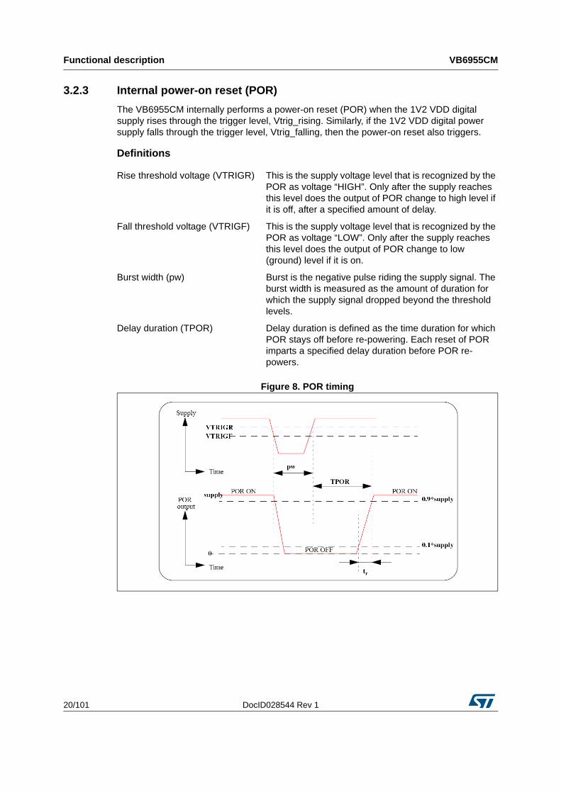
3.2.3 Internal power-on reset (POR)
The VB6955CM internally performs a power-on reset (POR) when the 1V2 VDD digital supply rises through the trigger level, Vtrig_rising. Similarly, if the 1V2 VDD digital power supply falls through the trigger level, Vtrig_falling, then the power-on reset also triggers.
Definitions
Figure 8. POR timing
Rise threshold voltage (VTRIGR) This is the supply voltage level that is recognized by the POR as voltage “HIGH”. Only after the supply reaches this level does the output of POR change to high level if it is off, after a specified amount of delay.
Fall threshold voltage (VTRIGF) This is the supply voltage level that is recognized by the POR as voltage “LOW”. Only after the supply reaches this level does the output of POR change to low (ground) level if it is on.
Burst width (pw) Burst is the negative pulse riding the supply signal. The burst width is measured as the amount of duration for which the supply signal dropped beyond the threshold levels.
Delay duration (TPOR) Delay duration is defined as the time duration for which POR stays off before re-powering. Each reset of POR imparts a specified delay duration before POR re-powers.
DocID028544 Rev 1 21/101
VB6955CM Functional description
22
3.2.4 Power off
The power off state is defined as either or both of the digital and analog supplies not present.
3.2.5 Hardware standby
This is the lowest power consumption mode. CCI communications are not supported in this mode. The PLL and the video blocks are powered down. This state is entered by stopping the external clock. All registers are returned to their default values
3.2.6 Software standby
Software standby mode preserves the contents of the CCI register map. CCI communications are supported in this mode. The software standby mode is selected using a serial interface command. If this state is entered from hardware standby, the data pads remain at LP-00. If this state is entered from streaming then the data pads go to LP-11 at the end of the current frame. The internal video timing is reset to the start of a video frame in preparation for the enabling of active video. The values of the serial interface registers such as exposure and gain are preserved. The system clock must remain active when communicating with the sensor.
This state is entered by releasing the device from hard reset by writing 0x00 to the mode control register (0x0100) or commanding a soft reset by writing 0x01 to the software reset register (0x0103).
Note: After a soft reset, all registers are returned to their default values.
3.2.7 Streaming
The VB6955CM streams live video. This mode is entered by writing 0x01 to the mode control register (0x0100).
Table 8. POR cell characteristics
Symbol Constraint Minimum Typical Maximum Units
VTRIGR POR rise voltage detection 0.95 V
VTRIGF POR fall voltage detection 0.4 V
Tburst (pw) Burst filter 2 8 µs
Tpor Delay duration 20 45 µs
Functional description VB6955CM
22/101 DocID028544 Rev 1
3.2.8 Fast standby mode
The fast software standby mode can be controlled using register 0x0106. By default it is disabled.
If this mode is disabled (that is, standard mode is enabled) and the software standby command is issued while streaming, the transmission of the current frame completes before the VB6955CM enters software standby.
If fast software standby mode is enabled, there are three possibilities for where the VB6955CM may be in the frame that is being read out when the command to go to software standby is received:
• command received during frame blanking
There is no difference in this situation if fast standby mode is enabled or disabled. The VB6955CM immediately enters software standby.
• command received during the active line
In CCP2 mode, the VB6955CM outputs the current line including the line end code and then terminates the frame by transmitting a line start code and a frame end code. The VB6955CM then immediately enters software standby mode.
In CSI-2 mode, the VB6955CM outputs the current packet and terminates the frame with a frame end packet. The VB6955CM then immediately enters software standby mode.
• command received during the line blanking
In CCP2 mode, the VB6955CM terminates the frame by transmitting a line start code and a frame end code. The VB6955CM then immediately enters software standby mode.
In CSI-2 mode, as the VB6955CM is already in an LP idle state, the VB6955CM immediately enters software standby mode.
DocID028544 Rev 1 23/101
VB6955CM Camera control interface (CCI)
50
4 Camera control interface (CCI)
This chapter specifies the camera control interface (CCI). The I2C-type interface uses 1.8 V I/O with two signals: serial data line (SDA) and serial clock line (SCL). CCI is used for control data transfer. Clock signal (SCL) generation is performed by the master device (the camera module is a slave device). The master device initiates data transfer. The CCI bus on the camera module has a maximum speed of 400 Kbits/s and has a software switchable device address. The default device address is 0x20.
Any internal register that can be written to, can also be read from. There are also read only registers that contain device status information, for example, design revision details. A read instruction from an unused register location returns the value 0x00. A read instruction from a reserved address may return any value. A write instruction to a reserved or unused register location is illegal and the effect of such a write is undefined. It is the responsibility of the host system to only write to register locations which have been defined.
4.1 Valid register data types
The contents of the registers can represent a number of different data types (see Table 9). The register map uses this coding to help with the interpretation of the contents of each register.
Table 9. Valid register data types
Data type Name Range Description
8UI 8-bit unsigned integer 0 to 255 -
8SI 8-bit signed integer -128 to 127 Two’s complement notation
16UI 16-bit unsigned integer 0 to 65535 -
16SI 16-bit signed integer -32768 to 32767 Two’s complement notation
16UR 16-bit unsigned iReal 0 to 255.9960937508.08 fixed point number. 8 integer bits (MS Byte), 8 fractional bits (LS Byte)
16SR 16-bit signed iReal -128 to 127.9960375Two’s complement notation, 8 fractional bits
32UR 32-bit unsigned iReal 0 to 65535.9999847416.16 fixed point number. 16 integer bits (MS 2 Bytes), 16 fractional bits (LS 2 Bytes)
32SF32-bit IEEE floating-point number
As per IEEE 754As per IEEE 754. 1 sign bit, 8 exponent bits, 23 fractional bits
8C or 16C 8-bit or 16-bit coded -This indicates that the value is decoded to select one of several functions or modes.
8B or 16B 8 or 16 bits -bEach bit represents a specific function or mode.
Camera control interface (CCI) VB6955CM
24/101 DocID028544 Rev 1
4.2 Register map
The registers default values are expressed as hexadecimal numbers.
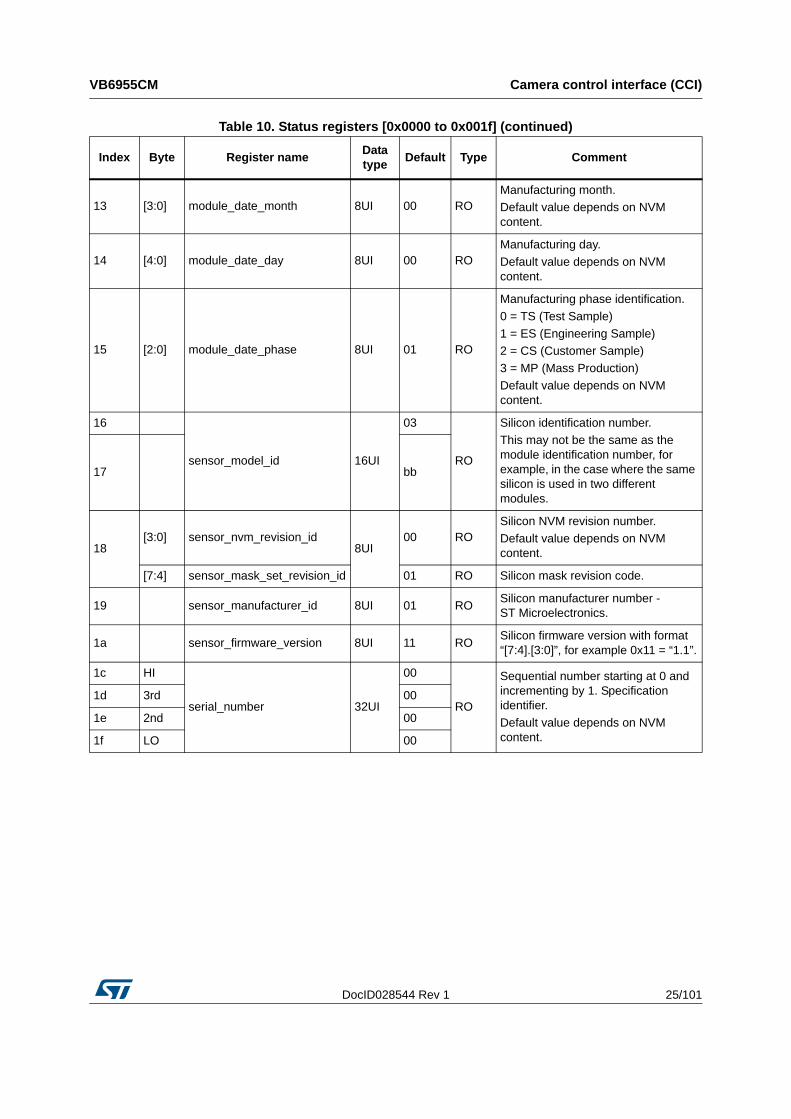
4.2.1 Status registers [0x0000 to 0x001f]
Table 10. Status registers [0x0000 to 0x001f]
Index Byte Register nameData type
Default Type Comment
0 Hi
module_model_id 16UI
07
RO
1955
Camera model identification number.
Default values depend on NVM content.
1 LO a3
2 revision_number_major 8UI 00 RO
Revision identifier of the camera for DCC change.
Default value depends on NVM content.
3 manufacturer_id 8UI 01 ROModule manufacturer number.
Default value depends on NVM content.
4 smia_version 8UI 0a ROSMIA version that sensor complies with
10 - Version 1.0
5 frame_count 8UI ff RWFrame count register. Increments from 1 to 254 when streaming. Reports 255 when idle.
6 pixel_order 8UI 00 RO
Color pixel readout order. Changes with mirror and flip (register 0x0101).
0x00 - GR/BG normal.
0x01 - RG/GB horizontal mirror.
0x02 - BG/GR vertical flip.
0x03 - GB/RG vertical flip and horizontal mirror.
8 HIdata_pedestal 16UI
00RO Offset applied to the video data.
9 LO 40
c pixel_depth 8UI 0a RO Pixel depth resolution of the sensor.
10 revision_number_minor 8UI 00 RO
Revision identifier of the camera for minor changes.
Default value depends on NVM content.
11 additional_spec_ver 8UI 08 RO Additional specification identifier.
12 [3:0] module_date_year 8UI 00 ROLast digit of manufacturing year.
Default value depends on NVM content.
DocID028544 Rev 1 25/101
VB6955CM Camera control interface (CCI)
50
13 [3:0] module_date_month 8UI 00 ROManufacturing month.
Default value depends on NVM content.
14 [4:0] module_date_day 8UI 00 ROManufacturing day.
Default value depends on NVM content.
15 [2:0] module_date_phase 8UI 01 RO
Manufacturing phase identification.
0 = TS (Test Sample)
1 = ES (Engineering Sample)
2 = CS (Customer Sample)
3 = MP (Mass Production)
Default value depends on NVM content.
16
sensor_model_id 16UI
03
RO
Silicon identification number.
This may not be the same as the module identification number, for example, in the case where the same silicon is used in two different modules.
17 bb
18[3:0] sensor_nvm_revision_id
8UI00 RO
Silicon NVM revision number.
Default value depends on NVM content.
[7:4] sensor_mask_set_revision_id 01 RO Silicon mask revision code.
19 sensor_manufacturer_id 8UI 01 ROSilicon manufacturer number - ST Microelectronics.
1a sensor_firmware_version 8UI 11 ROSilicon firmware version with format “[7:4].[3:0]”, for example 0x11 = “1.1”.
1c HI
serial_number 32UI
00
RO
Sequential number starting at 0 and incrementing by 1. Specification identifier.
Default value depends on NVM content.
1d 3rd 00
1e 2nd 00
1f LO 00
Table 10. Status registers [0x0000 to 0x001f] (continued)
Index Byte Register nameData type
Default Type Comment
Camera control interface (CCI) VB6955CM
26/101 DocID028544 Rev 1
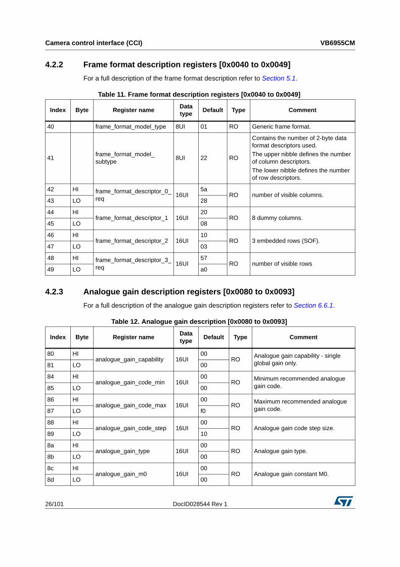
4.2.2 Frame format description registers [0x0040 to 0x0049]
For a full description of the frame format description refer to Section 5.1.
4.2.3 Analogue gain description registers [0x0080 to 0x0093]
For a full description of the analogue gain description registers refer to Section 6.6.1.
Table 11. Frame format description registers [0x0040 to 0x0049]
Index Byte Register nameData type
Default Type Comment
40 frame_format_model_type 8UI 01 RO Generic frame format.
41frame_format_model_ subtype
8UI 22 RO
Contains the number of 2-byte data format descriptors used.
The upper nibble defines the number of column descriptors.
The lower nibble defines the number of row descriptors.
42 HI frame_format_descriptor_0_req
16UI5a
RO number of visible columns.43 LO 28
44 HIframe_format_descriptor_1 16UI
20RO 8 dummy columns.
45 LO 08
46 HIframe_format_descriptor_2 16UI
10RO 3 embedded rows (SOF).
47 LO 03
48 HI frame_format_descriptor_3_req
16UI57
RO number of visible rows49 LO a0
Table 12. Analogue gain description [0x0080 to 0x0093]
Index Byte Register nameData type
Default Type Comment
80 HIanalogue_gain_capability 16UI
00RO
Analogue gain capability - single global gain only.81 LO 00
84 HIanalogue_gain_code_min 16UI
00RO
Minimum recommended analogue gain code.85 LO 00
86 HIanalogue_gain_code_max 16UI
00RO
Maximum recommended analogue gain code.87 LO f0
88 HIanalogue_gain_code_step 16UI
00RO Analogue gain code step size.
89 LO 10
8a HIanalogue_gain_type 16UI
00RO Analogue gain type.
8b LO 00
8c HIanalogue_gain_m0 16UI
00RO Analogue gain constant M0.
8d LO 00
DocID028544 Rev 1 27/101
VB6955CM Camera control interface (CCI)
50
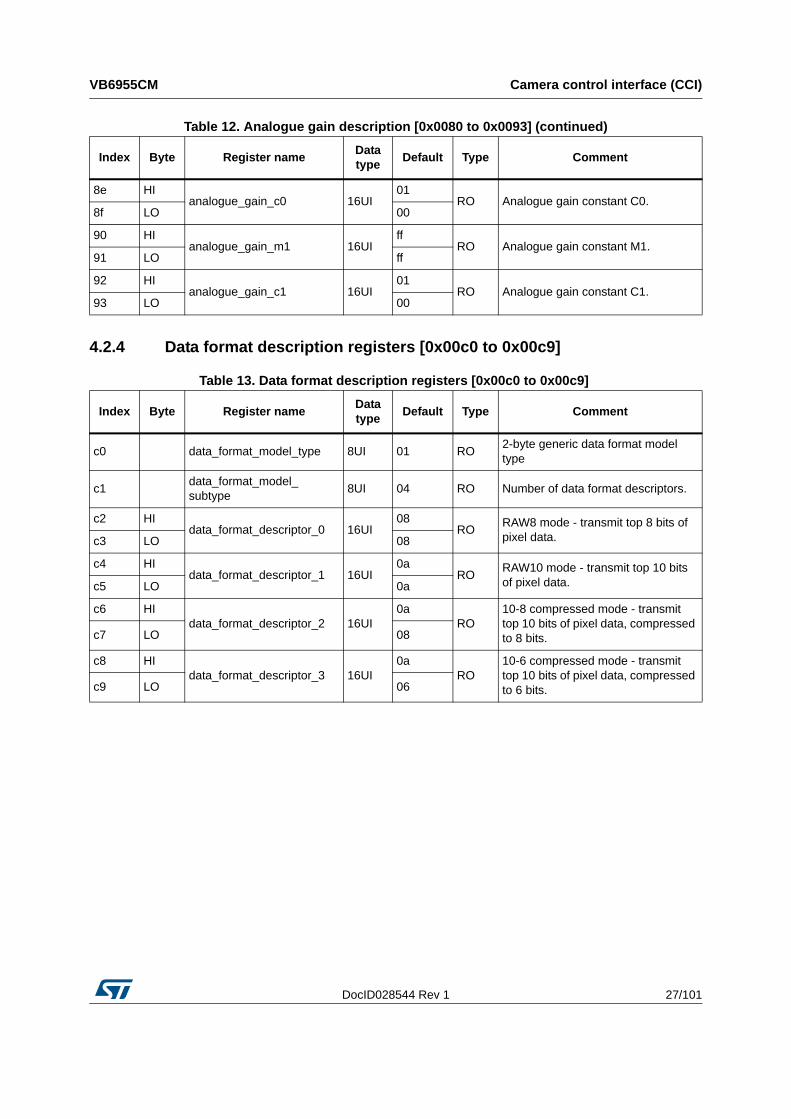
4.2.4 Data format description registers [0x00c0 to 0x00c9]
8e HIanalogue_gain_c0 16UI
01RO Analogue gain constant C0.
8f LO 00
90 HIanalogue_gain_m1 16UI
ffRO Analogue gain constant M1.
91 LO ff
92 HIanalogue_gain_c1 16UI
01RO Analogue gain constant C1.
93 LO 00
Table 12. Analogue gain description [0x0080 to 0x0093] (continued)
Index Byte Register nameData type
Default Type Comment
Table 13. Data format description registers [0x00c0 to 0x00c9]
Index Byte Register nameData type
Default Type Comment
c0 data_format_model_type 8UI 01 RO2-byte generic data format model type
c1data_format_model_ subtype
8UI 04 RO Number of data format descriptors.
c2 HIdata_format_descriptor_0 16UI
08RO
RAW8 mode - transmit top 8 bits of pixel data.c3 LO 08
c4 HIdata_format_descriptor_1 16UI
0aRO
RAW10 mode - transmit top 10 bits of pixel data.c5 LO 0a
c6 HIdata_format_descriptor_2 16UI
0aRO
10-8 compressed mode - transmit top 10 bits of pixel data, compressed to 8 bits.c7 LO 08
c8 HIdata_format_descriptor_3 16UI
0aRO
10-6 compressed mode - transmit top 10 bits of pixel data, compressed to 6 bits.c9 LO 06
Camera control interface (CCI) VB6955CM
28/101 DocID028544 Rev 1
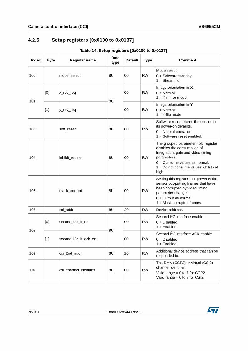
4.2.5 Setup registers [0x0100 to 0x0137]
Table 14. Setup registers [0x0100 to 0x0137]
Index Byte Register nameData type
Default Type Comment
100 mode_select 8UI 00 RWMode select.
0 = Software standby. 1 = Streaming.
101
[0] x_rev_req
8UI
00 RWImage orientation in X.
0 = Normal 1 = X-mirror mode.
[1] y_rev_req 00 RWImage orientation in Y.
0 = Normal 1 = Y-flip mode.
103 soft_reset 8UI 00 RW
Software reset returns the sensor to its power-on defaults.
0 = Normal operation. 1 = Software reset enabled.
104 inhibit_retime 8UI 00 RW
The grouped parameter hold register disables the consumption of integration, gain and video timing parameters.
0 = Consume values as normal. 1 = Do not consume values whilst set high.
105 mask_corrupt 8UI 00 RW
Setting this register to 1 prevents the sensor out-putting frames that have been corrupted by video timing parameter changes.
0 = Output as normal. 1 = Mask corrupted frames.
107 cci_addr 8UI 20 RW Device address.
108
[0] second_i2c_if_en
8UI
00 RWSecond I2C interface enable.
0 = Disabled 1 = Enabled
[1] second_i2c_if_ack_en 00 RWSecond I2C interface ACK enable.
0 = Disabled 1 = Enabled
109 cci_2nd_addr 8UI 20 RWAdditional device address that can be responded to.
110 csi_channel_identifier 8UI 00 RW
The DMA (CCP2) or virtual (CSI2) channel identifier.
Valid range = 0 to 7 for CCP2. Valid range = 0 to 3 for CSI2.

DocID028544 Rev 1 29/101
VB6955CM Camera control interface (CCI)
50
111 csi_signalling_mode 8UI 02 RW
Determines which transmission signalling mode is to be used.
0 = CCP2 data-clock signaling. 1 = CCP2 data-strobe signaling. 2 = CSI2.
112 HI
csi_data_format 16UI
0a
RW
The value of this register contains the pixel width of the uncompressed pixel data.
Valid values are 0xA and 0x8.
113 LO 0a
The value of this register contains the pixel width of the compressed pixel data.
Valid values are 0xA and 0x8.
114 csi_lane_mode 8UI 01 RWNumber of data lanes in use.
0 = 1-lane. 1 = 2-lane.
115 csi2_10_to_8_dt 8UI 30 RWCSI-2 data type for 10-to-8 compression.
117 csi2_10_to_6_dt 8UI 31 RWCSI-2 data type for 10-to-6 compression.
120 gain_mode 8UI 00 ROGlobal gain mode - this device only supports 0x00.
130 HIvana_voltage 16UR
02RW Typical supplied VANA voltage.
131 LO cc
132 HIvdig_voltage 16UR
01RW Typical supplied VDIG voltage.
133 LO cc
134 HIvio_voltage 16UR
01RW Typical IO voltage.
135 LO cc
136 HIext_clkfreq 16UR
06RW
8.8 fixed-point representation of the external clock-frequency, in MHz.137 LO 00
Table 14. Setup registers [0x0100 to 0x0137] (continued)
Index Byte Register nameData type
Default Type Comment
Camera control interface (CCI) VB6955CM
30/101 DocID028544 Rev 1
4.2.6 Integration and gain registers [0x0200 to 0x0215]
These registers are used to control the image exposure. See Section 6.6 for more information.
4.2.7 Video timing registers [0x0300 to 0x0387]
For a full description of the video timing registers refer to Chapter 5.
Table 15. Integration and gain registers [0x0200 to 0x0215]
Index Byte Register nameData type
Default Type Comment
200 HIfine_exp_req 16UI
02RW Fine integration time in pixels.
201 LO ae
202 HIcoarse_exp_req 16UI
00RW Coarse integration time in lines.
203 LO 00
204 gain_req_dummy_hi 8UI 00 RODummy HI byte to ensure presence in SLC test
205 gain_req 8UI 00 RW Gain code for all channels.
20e HIdigital_gain_greenR 16UR
01RW
Green (red row) channel digital gain value20f LO 00
210 HIdigital_gain_red 16UR
01RW Red channel digital gain value
211 LO 00
212 HIdigital_gain_blue 16UR
01RW Blue channel digital gain value
213 LO 00
214 HIdigital_gain_greenB 16UR
01RW
Green (blue row) channel digital gain value.215 LO 00
Table 16. Video timing registers [0x0300 to 0x0387]
Index Byte Register nameData type
Default Type Comment
300 vt_pix_clk_div_dummy_hi 8UI 00 RODummy HI byte to ensure presence in SLC.
301 vt_pix_clk_div 8UI 0a RW Video timing pixel clock divider.
302 vt_sys_clk_div_dummy_hi 8UI 00 RODummy HI byte to ensure presence in SLC.
303 vt_sys_clk_div 8UI 01 RW Video timing system clock divider.
304 pre_pll_div_dummy_hi 8UI 00 RODummy HI byte to ensure presence in SLC.
305 pre_pll_div 8UI 01 RW
Pre-PLL clock divider value.
1 = Divide EXTCLK by 1. 2 = Divide EXTCLK by 2. 4 = Divide EXTCLK by 4.
DocID028544 Rev 1 31/101
VB6955CM Camera control interface (CCI)
50
306 pll_mult_dummy_hi 8UI 00 RODummy HI byte to ensure presence in SLC.
307 pll_mult 8UI 85 RW
PLL multiplier value.
Odd and even values can be used, but odd values result in the nearest lower even value being used (for example, 133 becomes 132).
308 op_pix_clk_div_dummy_hi 8UI 00 RODummy HI byte to ensure presence in SLC.
309 op_pix_clk_div 8UI 0a RW Output timing pixel clock divider.
30a op_sys_clk_div_dummy_hi 8UI 00 RODummy HI byte to ensure presence in SLC.
30b op_sys_clk_div 8UI 01 RW Output timing system clock divider.
340 HIframe_length_req 16UI
08RW Length of the video frame in lines.
341 LO 24
342 HIline_length_req 16UI
0aRW Length of a line of video in pixels.
343 LO be
344 HIx_start_req 16UI
00RW
X pixel address of the top left corner of the visible pixel data.345 LO 00
346 HIy_start_req 16UI
00RW
Y line address of the top left corner of the visible pixel data.347 LO 00
348 HIx_end_req 16UI
0aRW
X pixel address of the bottom right corner of the visible pixel data.349 LO 27
34a HIy_end_req 16UI
07RW
Y line address of bottom right corner of the visible pixel data.34b LO 9f
34c HIx_op_size_req 16UI
0aRW
Width in pixels of the output image from the sensor.34d LO 28
34e HIy_op_size_req 16UI
07RW
Height in lines of the output image from the sensor.34f LO a0
380 x_even_inc_req_dummy_hi 8UI 00 RODummy HI byte to ensure presence in SLC Test
381 x_even_inc_req 8UI 01 RW X address increment for even pixels.
382 x_odd_inc_req_dummy_hi 8UI 00 RODummy HI byte to ensure presence in SLC test
383 x_odd_inc_req 8UI 01 RW X address increment for odd pixels.
384 y_even_inc_req_dummy_hi 8UI 00 RODummy HI byte to ensure presence in SLC test
Table 16. Video timing registers [0x0300 to 0x0387] (continued)
Index Byte Register nameData type
Default Type Comment
Camera control interface (CCI) VB6955CM
32/101 DocID028544 Rev 1
4.2.8 Scaler and digital crop registers [0x0400 to 0x040f]
385 y_even_inc_req 8UI 01 RW Y address increment for even lines.
386 y_odd_inc_req_dummy_hi 8UI 00 RODummy HI byte to ensure presence in SLC test
387 y_odd_inc_req 8UI 01 RW Y address increment for odd lines.
Table 16. Video timing registers [0x0300 to 0x0387] (continued)
Index Byte Register nameData type
Default Type Comment
Table 17. Scaler and digital crop registers [0x0400 to 0x040f]
Index Byte Register nameData type
Default Type Comment
400 scale_mode_req_dummy_hi 8UI 00 RO
401 scale_mode_req 8UI 00 RWScaling mode
0 = No scaling 1 = Horizontal scaling
402scale_cosite_req_dummy_ hi
8UI 00 RO
403 scale_cosite_req 8UI 00 RW
Spatial sampling
0 = Bayer sampling 1 = Co-sited (2- or 4-component) 2 = Co-sited (3-component)
404 scale_m_req_dummy_hi 8UI 00 RO
405 scale_m_req 8UI 10 RW Down scale factor. M component.
406 HIscale_n 16UI
00RO Down scale factor. N component.
407 LO 10
408 HI
digital_crop_x_offset 16UI
00
RW
Offset from X-address of the top left corner of the visible pixel data after analog crop, bin and subsample. Even numbers only (pixels).
409 LO 00
40a HI
digital_crop_y_offset 16UI
00
RW
Offset from Y-address of the top left corner of the visible pixel data after analog crop, bin and subsample. Even numbers only (lines).
40b LO 00
40c HIdigital_crop_image_width 16UI
0aRW
Image width after digital crop. Even numbers only (pixels).40d LO 28
40e HIdigital_crop_image_height 16UI
07RW
Image height after digital crop. Even numbers only (lines).40f LO a0
DocID028544 Rev 1 33/101
VB6955CM Camera control interface (CCI)
50
4.2.9 Compression setup registers [0x0500 to 0x0501]
4.2.10 Test pattern registers [0x0600 to 0x0611]
Table 18. Compression setup registers [0x0500 to 0x0501]
Index Byte Register nameData type
Default Type Comment
500
501compression_algorithm 16UI
00RO
Compression algorithm is DPCM/PCM.01
Table 19. Test pattern registers [0x0600 to 0x0611]
Index Byte Register nameData type
Default Type Comment
600 man_spec_patt_req 8UI 00 RW
Enables maufacturer-specific test patterns.
0 = Enable SMIA test patterns. 1 = Enable manufacturer-specific test patterns.
601 test_pattern_req 8UI 00 RW
SMIA test pattern selector.
Note that the PN9 test pattern replaces data at output TX stage.
bit0 = No pattern bit1 = Solid color bit2 = 100% color bars bit3 = Fade-to-grey color bars bit4 = Pseudo random-PN9
602 HItest_data_red 16UI
00RW
Test data used to replace Red pixel data - range 0 to 1023.603 LO 00
604 HItest_data_greenr 16UI
00RW
Test data used to replace Green pixel data on lines that also have Red pixels - range 0 to 1023.605 LO 00
606 HItest_data_blue 16UI
00RW
Test data used to replace Blue pixel data - range 0 to 1023.607 LO 00
608 HItest_data_greenb 16UI
00RW
Test data used to replace Green pixel data on lines that also have Blue pixels - range 0 to 1023.609 LO 00
60a HItest_hcur_width 16UI
00RW
Defines the width in pixels of the horizontal cursor.60b LO 00
60c HItest_hcur_posn 16UI
00RW
Defines the position of the top edge of the horizontal cursor.60d LO 00
60e HItest_vcur_width 16UI
00RW
Defines the width in pixels of the vertical cursor. 60f LO 00
Camera control interface (CCI) VB6955CM
34/101 DocID028544 Rev 1
4.2.11 CSI2 registers [0x808]
4.2.12 DPHY registers [0x820 to 0x823]
610 HI
test_vcur_posn 16UI
00
RW
Defines the left hand edge of the vertical cursor
The value can be set to 0xFFFF which enables an automatic mode whereby the cursor advances every frame.
Can be used to visually check the frame count.
611 LO 00
Table 19. Test pattern registers [0x0600 to 0x0611] (continued)
Index Byte Register nameData type
Default Type Comment
Table 20. CSI2 registers [0x808]
Index Byte Register nameData type
Default Type Comment
808 dphy_ctrl 8UI 00 RWCSI2 DPHY control
1 = Use UI control. 2 = Use register control.
Table 21. DPHY registers [0x820 to 0x823]
Index Byte Register nameData type
Default Type Comment
820 HI
dphy_channel_mbps_for_ui 32UR00.00
00.00RW
CSI2 DPHY requested (target) channel rate in Mbps (16.16 fixed-point representation)
This is used to calculate the DPHY unit-interval (UI) value.
It does not control the sensor clock setup, but should normally correspond to those settings.
0 = Sensor automatically calculates UI from host-programmed EXTCLK and clock divider values and reports in MAN_SPEC_DPHY__CLKLANE_ UIX4 register. 80-800 = Sensor calculates UI from Mbps value.
821 3rd
822 2nd
823 LO
DocID028544 Rev 1 35/101
VB6955CM Camera control interface (CCI)
50
4.2.13 Binning registers [0x900 to 0x902]
4.2.14 Data transfer registers [0x0a00 to 0x0a43]
Table 22. Binning registers [0x900 to 0x902]
Index Byte Register nameData type
Default Type Comment
900 binning_mode 8UI 00 RWBinning mode.
0 = Disabled 1 = Enabled
901 binning_type 8UI 00 RWHigh-nibble = Column binning factor. High-nibble = Row binning factor.
902 binning_weighting 8UI 00 RWBinning weighting type:
0 = Averaged.
Table 23. Data transfer registers [0x0a00 to 0x0a43]
Index Byte Register nameData type
Default Type Comment
a00 data_xfer_if1_ctrl 8UI 00 RW
bit0: 0 = Disable Xfer IF1. 1 = Enable Xfer IF1.
bit1: 0 = Read enable on IF1 1 = Write enable on IF1
bit2: 0 = Disabled 1 = Clear error bits on IF1
a01 data_xfer_if1_status 8UI 00 RO
bit0: Read IF ready
bit1: Write IF ready.
bit2: Data corrupt.
bit3: Improper IF usage.
a02 data_xfer_if1_page_select 8UI 00 RWSelect RW Pages from 0 to 255 for IF1.
a04 DataXfer_Data0 8UI 00 RW Data Xfer Interface - DataLoc0
-- -- --
a43 DataXfer_Data63 8UI 00 RW Data Xfer Interface - DataLoc63
Camera control interface (CCI) VB6955CM
36/101 DocID028544 Rev 1
4.2.15 Ideal raw registers [0x0b04 to 0x0b05]
4.2.16 Flash registers [0x0c12 to 0x0c2a]
Table 24. Ideal raw registers [0x0b04 to 0x0b05]
Index Byte Register nameData type
Default Type Comment
b04black_level_correction_ enable
8UI 01 RWBlack level correction.
0 = Disabled 1 = Enabled
b05mapped_couplet_correct_enable
8UI 01 RWMapped couplet correction enable.
0 = Disabled 1 = Enabled
Table 25. Flash registers [0x0c12 to 0x0c2a]
Index Byte Register nameData type
Default Type Comment
c12 flash_strobe_adjustment 8UI 00 RWRegister to control pre-divider for flash_strobe_width counter.
c14 HIflash_strobe_start_point 16UI
00RW
Register to select reference point for flash strobe. Adjustable in one line steps. Range 0 - last line.c15 LO 00
c16 HI tFlash_strobe_delay_rs_ ctrl
16UI00
RW 1H step. 0-65535.c17 LO 00
c18 HI tFlash_strobe_width_high_rs_ctrl
16UI00
RWUsed to control flash strobe width in rolling shutter mode. 1-65535.c19 LO 00
c1a Flash_mode_rs 8UI 00 RW
Bit[0] - Flash mode (rolling shutter):
0 = strobe usage in single trigger mode. 1 = strobe usage in continuous mode.
c1b Flash_trigger_rs 8UI 00 RW
Bit[0] - Flash trigger (rolling shutter):
0 = disable strobe generation. 1 = trigger flash (auto clear in single mode).
c1c Flash_status 8UI 00 RO
Bit[0] - Flash status:
0 = flash strobe is not retimed to this frame. 1 = flash strobe is retimed to this frame.
Bit[1]:
0 = flash is not active in global reset. 1 = flash is active in global reset mode.
DocID028544 Rev 1 37/101
VB6955CM Camera control interface (CCI)
50
4.2.17 Sensor - high level auto focus registers [0x0d80 to 0x0d89]
c26 HI tFlash_strobe_width_ high_rs_ctrl
16UI00
RWUsed to control flash strobe width in rolling shutter mode. 1-65535. c27 LO 00
c28 HI tFlash_strobe_width_low_ rs_ctrl
16UI00
RWUsed to control flash strobe width in rolling shutter mode. 1-65535. c29 LO 00
c2atFlash_strobe_count_rs_ ctrl
8UI 00 RWUsed to control flash strobe width in rolling shutter mode. 1-255.
Table 25. Flash registers [0x0c12 to 0x0c2a] (continued)
Index Byte Register nameData type
Default Type Comment
Table 26. Sensor - high level auto focus registers [0x0d80 to 0x0d89]
Index Byte Register nameData type
Default Type Comment
d80 HIFOCUS_CHANGE 16UI
00RW
This register is used to change the focus point.d81 LO 00
d82 HIFOCUS_CHANGE_CONTROL
16UI00
RWBit[0] - fcc_enable
Bit[9] - Automatic ringing compensation enabled83 LO 00
d84 HIFOCUS_CHANGE_NUMBER_ PHASE1
16UI
00
RW
Specifies the increased or decreased value from focus change register and specifies the amount of focus change at each strobe. Applicable for phase 1 sequence.
d85 LO 00
d86 HIFOCUS_CHANGE_NUMBER_ PHASE2
16UI
00
RW
Specifies the increased or decreased value from focus change register and specifies the amount of focus change at each strobe. Applicable for phase 2 sequence.
d87 LO 00
d88STROBE_COUNT_PHASE1
8UI 00 RWSpecifies how many strobes are counted during Phase1 of two types of sequences.
d89STROBE_COUNT_PHASE2
8UI 00 RWSpecifies how many strobes are counted for Phase2 sequence.
Camera control interface (CCI) VB6955CM
38/101 DocID028544 Rev 1
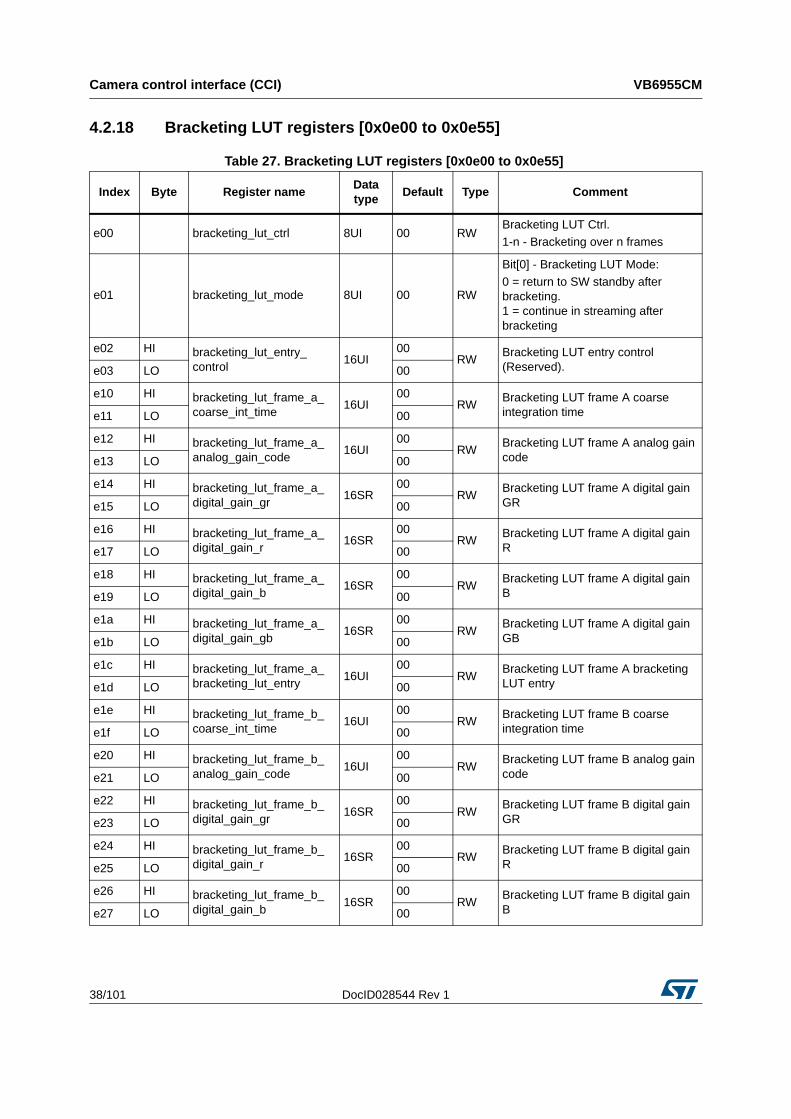
4.2.18 Bracketing LUT registers [0x0e00 to 0x0e55]
Table 27. Bracketing LUT registers [0x0e00 to 0x0e55]
Index Byte Register nameData type
Default Type Comment
e00 bracketing_lut_ctrl 8UI 00 RWBracketing LUT Ctrl.
1-n - Bracketing over n frames
e01 bracketing_lut_mode 8UI 00 RW
Bit[0] - Bracketing LUT Mode:
0 = return to SW standby after bracketing. 1 = continue in streaming after bracketing
e02 HI bracketing_lut_entry_ control
16UI00
RWBracketing LUT entry control (Reserved).e03 LO 00
e10 HI bracketing_lut_frame_a_ coarse_int_time
16UI00
RWBracketing LUT frame A coarse integration timee11 LO 00
e12 HI bracketing_lut_frame_a_ analog_gain_code
16UI00
RWBracketing LUT frame A analog gain codee13 LO 00
e14 HI bracketing_lut_frame_a_ digital_gain_gr
16SR00
RWBracketing LUT frame A digital gain GRe15 LO 00
e16 HI bracketing_lut_frame_a_ digital_gain_r
16SR00
RWBracketing LUT frame A digital gain Re17 LO 00
e18 HI bracketing_lut_frame_a_ digital_gain_b
16SR00
RWBracketing LUT frame A digital gain Be19 LO 00
e1a HI bracketing_lut_frame_a_ digital_gain_gb
16SR00
RWBracketing LUT frame A digital gain GBe1b LO 00
e1c HI bracketing_lut_frame_a_ bracketing_lut_entry
16UI00
RWBracketing LUT frame A bracketing LUT entrye1d LO 00
e1e HI bracketing_lut_frame_b_ coarse_int_time
16UI00
RWBracketing LUT frame B coarse integration timee1f LO 00
e20 HI bracketing_lut_frame_b_ analog_gain_code
16UI00
RWBracketing LUT frame B analog gain codee21 LO 00
e22 HI bracketing_lut_frame_b_ digital_gain_gr
16SR00
RWBracketing LUT frame B digital gain GRe23 LO 00
e24 HI bracketing_lut_frame_b_ digital_gain_r
16SR00
RWBracketing LUT frame B digital gain Re25 LO 00
e26 HI bracketing_lut_frame_b_ digital_gain_b
16SR00
RWBracketing LUT frame B digital gain Be27 LO 00
DocID028544 Rev 1 39/101
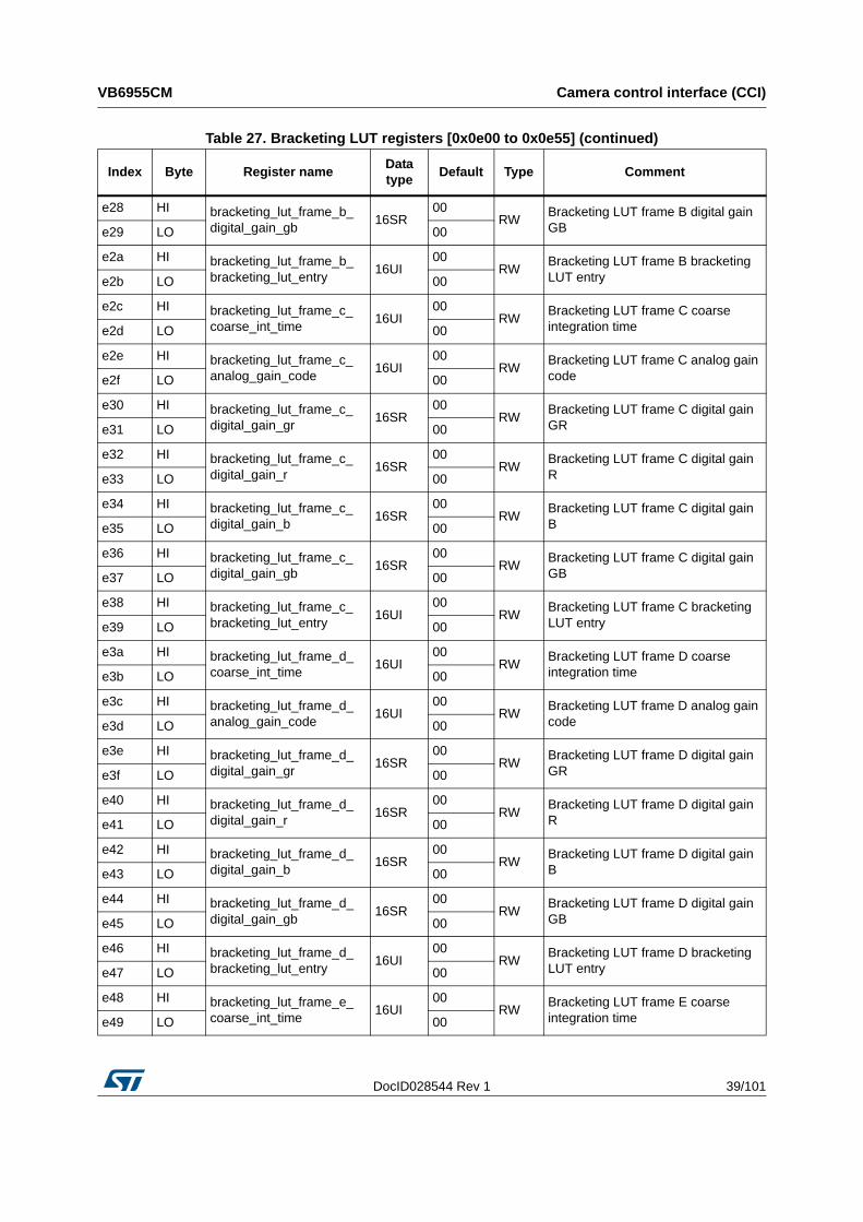
VB6955CM Camera control interface (CCI)
50
e28 HI bracketing_lut_frame_b_ digital_gain_gb
16SR00
RWBracketing LUT frame B digital gain GBe29 LO 00
e2a HI bracketing_lut_frame_b_ bracketing_lut_entry
16UI00
RWBracketing LUT frame B bracketing LUT entrye2b LO 00
e2c HI bracketing_lut_frame_c_ coarse_int_time
16UI00
RWBracketing LUT frame C coarse integration timee2d LO 00
e2e HI bracketing_lut_frame_c_ analog_gain_code
16UI00
RWBracketing LUT frame C analog gain codee2f LO 00
e30 HI bracketing_lut_frame_c_ digital_gain_gr
16SR00
RWBracketing LUT frame C digital gain GRe31 LO 00
e32 HI bracketing_lut_frame_c_ digital_gain_r
16SR00
RWBracketing LUT frame C digital gain Re33 LO 00
e34 HI bracketing_lut_frame_c_ digital_gain_b
16SR00
RWBracketing LUT frame C digital gain Be35 LO 00
e36 HI bracketing_lut_frame_c_ digital_gain_gb
16SR00
RWBracketing LUT frame C digital gain GBe37 LO 00
e38 HI bracketing_lut_frame_c_ bracketing_lut_entry
16UI00
RWBracketing LUT frame C bracketing LUT entrye39 LO 00
e3a HI bracketing_lut_frame_d_ coarse_int_time
16UI00
RWBracketing LUT frame D coarse integration timee3b LO 00
e3c HI bracketing_lut_frame_d_ analog_gain_code
16UI00
RWBracketing LUT frame D analog gain codee3d LO 00
e3e HI bracketing_lut_frame_d_ digital_gain_gr
16SR00
RWBracketing LUT frame D digital gain GRe3f LO 00
e40 HI bracketing_lut_frame_d_ digital_gain_r
16SR00
RWBracketing LUT frame D digital gain Re41 LO 00
e42 HI bracketing_lut_frame_d_ digital_gain_b
16SR00
RWBracketing LUT frame D digital gain Be43 LO 00
e44 HI bracketing_lut_frame_d_ digital_gain_gb
16SR00
RWBracketing LUT frame D digital gain GBe45 LO 00
e46 HI bracketing_lut_frame_d_ bracketing_lut_entry
16UI00
RWBracketing LUT frame D bracketing LUT entrye47 LO 00
e48 HI bracketing_lut_frame_e_ coarse_int_time
16UI00
RWBracketing LUT frame E coarse integration timee49 LO 00
Table 27. Bracketing LUT registers [0x0e00 to 0x0e55] (continued)
Index Byte Register nameData type
Default Type Comment
Camera control interface (CCI) VB6955CM
40/101 DocID028544 Rev 1
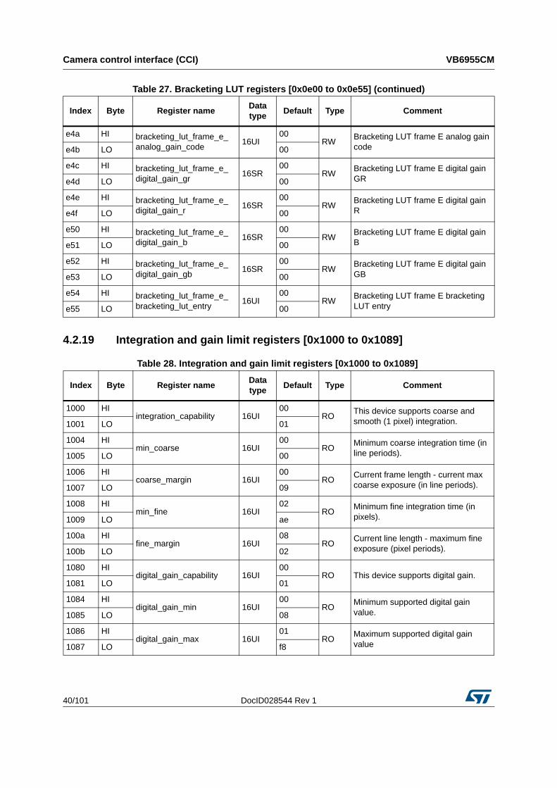
4.2.19 Integration and gain limit registers [0x1000 to 0x1089]
e4a HI bracketing_lut_frame_e_ analog_gain_code
16UI00
RWBracketing LUT frame E analog gain codee4b LO 00
e4c HI bracketing_lut_frame_e_ digital_gain_gr
16SR00
RWBracketing LUT frame E digital gain GRe4d LO 00
e4e HI bracketing_lut_frame_e_ digital_gain_r
16SR00
RWBracketing LUT frame E digital gain Re4f LO 00
e50 HI bracketing_lut_frame_e_ digital_gain_b
16SR00
RWBracketing LUT frame E digital gain Be51 LO 00
e52 HI bracketing_lut_frame_e_ digital_gain_gb
16SR00
RWBracketing LUT frame E digital gain GBe53 LO 00
e54 HI bracketing_lut_frame_e_ bracketing_lut_entry
16UI00
RWBracketing LUT frame E bracketing LUT entrye55 LO 00
Table 27. Bracketing LUT registers [0x0e00 to 0x0e55] (continued)
Index Byte Register nameData type
Default Type Comment
Table 28. Integration and gain limit registers [0x1000 to 0x1089]
Index Byte Register nameData type
Default Type Comment
1000 HIintegration_capability 16UI
00RO
This device supports coarse and smooth (1 pixel) integration.1001 LO 01
1004 HImin_coarse 16UI
00RO
Minimum coarse integration time (in line periods).1005 LO 00
1006 HIcoarse_margin 16UI
00RO
Current frame length - current max coarse exposure (in line periods).1007 LO 09
1008 HImin_fine 16UI
02RO
Minimum fine integration time (in pixels).1009 LO ae
100a HIfine_margin 16UI
08RO
Current line length - maximum fine exposure (pixel periods).100b LO 02
1080 HIdigital_gain_capability 16UI
00RO This device supports digital gain.
1081 LO 01
1084 HIdigital_gain_min 16UI
00RO
Minimum supported digital gain value.1085 LO 08
1086 HIdigital_gain_max 16UI
01RO
Maximum supported digital gain value1087 LO f8
DocID028544 Rev 1 41/101
VB6955CM Camera control interface (CCI)
50
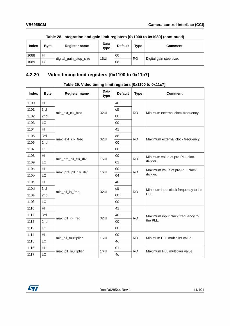
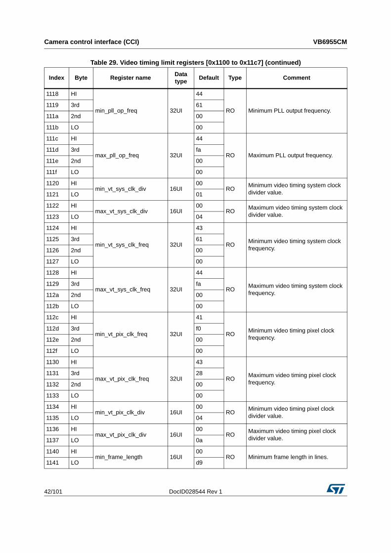
4.2.20 Video timing limit registers [0x1100 to 0x11c7]
1088 HIdigital_gain_step_size 16UI
00RO Digital gain step size.
1089 LO 08
Table 28. Integration and gain limit registers [0x1000 to 0x1089] (continued)
Index Byte Register nameData type
Default Type Comment
Table 29. Video timing limit registers [0x1100 to 0x11c7]
Index Byte Register nameData type
Default Type Comment
1100 HI
min_ext_clk_freq 32UI
40
RO Minimum external clock frequency.1101 3rd c0
1102 2nd 00
1103 LO 00
1104 HI
max_ext_clk_freq 32UI
41
RO Maximum external clock frequency.1105 3rd d8
1106 2nd 00
1107 LO 00
1108 HImin_pre_pll_clk_div 16UI
00RO
Minimum value of pre-PLL clock divider.1109 LO 01
110a HImax_pre_pll_clk_div 16UI
00RO
Maximum value of pre-PLL clock divider.110b LO 04
110c HI
min_pll_ip_freq 32UI
40
ROMinimum input clock frequency to the PLL.
110d 3rd c0
110e 2nd 00
110f LO 00
1110 HI
max_pll_ip_freq 32UI
41
ROMaximum input clock frequency to the PLL.
1111 3rd 40
1112 2nd 00
1113 LO 00
1114 HImin_pll_multiplier 16UI
00RO Minimum PLL multiplier value.
1115 LO 4c
1116 HImax_pll_multiplier 16UI
01RO Maximum PLL multiplier value.
1117 LO 4c
Camera control interface (CCI) VB6955CM
42/101 DocID028544 Rev 1
1118 HI
min_pll_op_freq 32UI
44
RO Minimum PLL output frequency.1119 3rd 61
111a 2nd 00
111b LO 00
111c HI
max_pll_op_freq 32UI
44
RO Maximum PLL output frequency.111d 3rd fa
111e 2nd 00
111f LO 00
1120 HImin_vt_sys_clk_div 16UI
00RO
Minimum video timing system clock divider value.1121 LO 01
1122 HImax_vt_sys_clk_div 16UI
00RO
Maximum video timing system clock divider value.1123 LO 04
1124 HI
min_vt_sys_clk_freq 32UI
43
ROMinimum video timing system clock frequency.
1125 3rd 61
1126 2nd 00
1127 LO 00
1128 HI
max_vt_sys_clk_freq 32UI
44
ROMaximum video timing system clock frequency.
1129 3rd fa
112a 2nd 00
112b LO 00
112c HI
min_vt_pix_clk_freq 32UI
41
ROMinimum video timing pixel clock frequency.
112d 3rd f0
112e 2nd 00
112f LO 00
1130 HI
max_vt_pix_clk_freq 32UI
43
ROMaximum video timing pixel clock frequency.
1131 3rd 28
1132 2nd 00
1133 LO 00
1134 HImin_vt_pix_clk_div 16UI
00RO
Minimum video timing pixel clock divider value.1135 LO 04
1136 HImax_vt_pix_clk_div 16UI
00RO
Maximum video timing pixel clock divider value.1137 LO 0a
1140 HImin_frame_length 16UI
00RO Minimum frame length in lines.
1141 LO d9
Table 29. Video timing limit registers [0x1100 to 0x11c7] (continued)
Index Byte Register nameData type
Default Type Comment
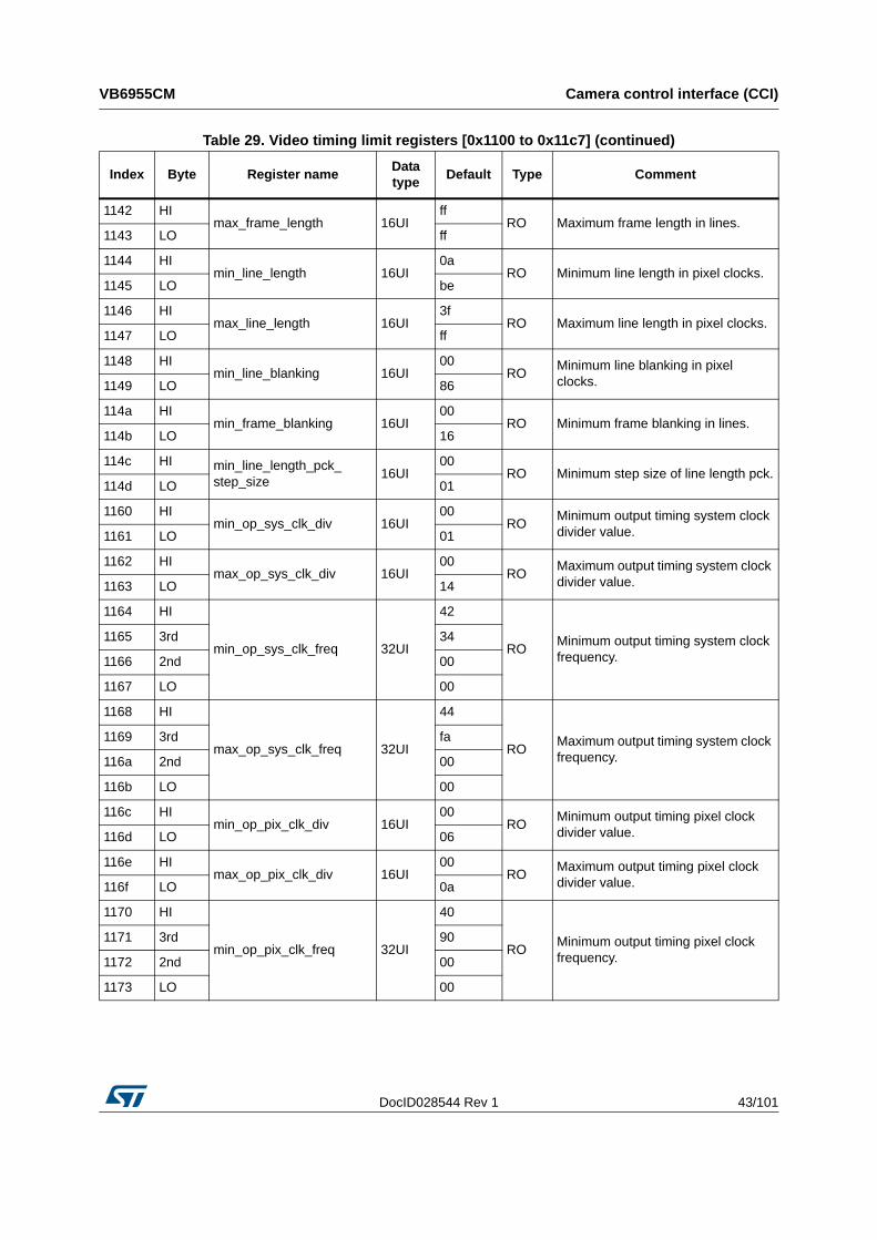
DocID028544 Rev 1 43/101
VB6955CM Camera control interface (CCI)
50
1142 HImax_frame_length 16UI
ffRO Maximum frame length in lines.
1143 LO ff
1144 HImin_line_length 16UI
0aRO Minimum line length in pixel clocks.
1145 LO be
1146 HImax_line_length 16UI
3fRO Maximum line length in pixel clocks.
1147 LO ff
1148 HImin_line_blanking 16UI
00RO
Minimum line blanking in pixel clocks.1149 LO 86
114a HImin_frame_blanking 16UI
00RO Minimum frame blanking in lines.
114b LO 16
114c HI min_line_length_pck_ step_size
16UI00
RO Minimum step size of line length pck.114d LO 01
1160 HImin_op_sys_clk_div 16UI
00RO
Minimum output timing system clock divider value.1161 LO 01
1162 HImax_op_sys_clk_div 16UI
00RO
Maximum output timing system clock divider value.1163 LO 14
1164 HI
min_op_sys_clk_freq 32UI
42
ROMinimum output timing system clock frequency.
1165 3rd 34
1166 2nd 00
1167 LO 00
1168 HI
max_op_sys_clk_freq 32UI
44
ROMaximum output timing system clock frequency.
1169 3rd fa
116a 2nd 00
116b LO 00
116c HImin_op_pix_clk_div 16UI
00RO
Minimum output timing pixel clock divider value.116d LO 06
116e HImax_op_pix_clk_div 16UI
00RO
Maximum output timing pixel clock divider value.116f LO 0a
1170 HI
min_op_pix_clk_freq 32UI
40
ROMinimum output timing pixel clock frequency.
1171 3rd 90
1172 2nd 00
1173 LO 00
Table 29. Video timing limit registers [0x1100 to 0x11c7] (continued)
Index Byte Register nameData type
Default Type Comment
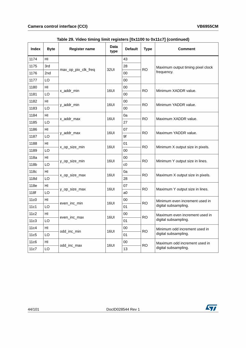
Camera control interface (CCI) VB6955CM
44/101 DocID028544 Rev 1
1174 HI
max_op_pix_clk_freq 32UI
43
ROMaximum output timing pixel clock frequency.
1175 3rd 28
1176 2nd 00
1177 LO 00
1180 HIx_addr_min 16UI
00RO Minimum XADDR value.
1181 LO 00
1182 HIy_addr_min 16UI
00RO Minimum YADDR value.
1183 LO 00
1184 HIx_addr_max 16UI
0aRO Maximum XADDR value.
1185 LO 27
1186 HIy_addr_max 16UI
07RO Maximum YADDR value.
1187 LO 9f
1188 HIx_op_size_min 16UI
01RO Minimum X output size in pixels.
1189 LO 00
118a HIy_op_size_min 16UI
00RO Minimum Y output size in lines.
118b LO c0
118c HIx_op_size_max 16UI
0aRO Maximum X output size in pixels.
118d LO 28
118e HIy_op_size_max 16UI
07RO Maximum Y output size in lines.
118f LO a0
11c0 HIeven_inc_min 16UI
00RO
Minimum even increment used in digital subsampling.11c1 LO 01
11c2 HIeven_inc_max 16UI
00RO
Maximum even increment used in digital subsampling.11c3 LO 01
11c4 HIodd_inc_min 16UI
00RO
Minimum odd increment used in digital subsampling.11c5 LO 01
11c6 HIodd_inc_max 16UI
00RO
Maximum odd increment used in digital subsampling.11c7 LO 13
Table 29. Video timing limit registers [0x1100 to 0x11c7] (continued)
Index Byte Register nameData type
Default Type Comment
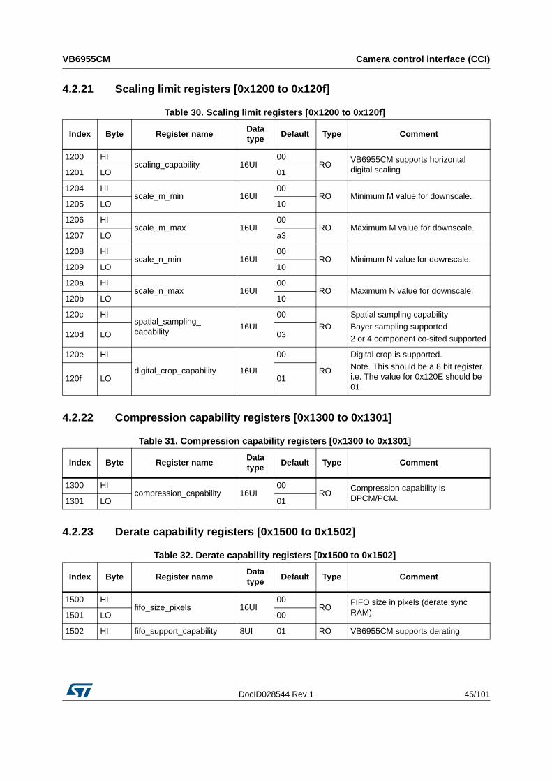
DocID028544 Rev 1 45/101
VB6955CM Camera control interface (CCI)
50
4.2.21 Scaling limit registers [0x1200 to 0x120f]
4.2.22 Compression capability registers [0x1300 to 0x1301]
4.2.23 Derate capability registers [0x1500 to 0x1502]
Table 30. Scaling limit registers [0x1200 to 0x120f]
Index Byte Register nameData type
Default Type Comment
1200 HIscaling_capability 16UI
00RO
VB6955CM supports horizontal digital scaling1201 LO 01
1204 HIscale_m_min 16UI
00RO Minimum M value for downscale.
1205 LO 10
1206 HIscale_m_max 16UI
00RO Maximum M value for downscale.
1207 LO a3
1208 HIscale_n_min 16UI
00RO Minimum N value for downscale.
1209 LO 10
120a HIscale_n_max 16UI
00RO Maximum N value for downscale.
120b LO 10
120c HIspatial_sampling_ capability
16UI
00
RO
Spatial sampling capability
Bayer sampling supported
2 or 4 component co-sited supported120d LO 03
120e HI
digital_crop_capability 16UI
00
RO
Digital crop is supported.
Note. This should be a 8 bit register. i.e. The value for 0x120E should be 01
120f LO 01
Table 31. Compression capability registers [0x1300 to 0x1301]
Index Byte Register nameData type
Default Type Comment
1300 HIcompression_capability 16UI
00RO
Compression capability is DPCM/PCM.1301 LO 01
Table 32. Derate capability registers [0x1500 to 0x1502]
Index Byte Register nameData type
Default Type Comment
1500 HIfifo_size_pixels 16UI
00RO
FIFO size in pixels (derate sync RAM).1501 LO 00
1502 HI fifo_support_capability 8UI 01 RO VB6955CM supports derating

Camera control interface (CCI) VB6955CM
46/101 DocID028544 Rev 1
4.2.24 DPHY capability registers [0x1600 to 0x1604]
4.2.25 Bitrate limit registers [0x1608 to 0x1617]
Table 33. DPHY capability registers [0x1600 to 0x1604]
Index Byte Register nameData type
Default Type Comment
1600 dphy_ctrl_capability 8UI 03 RO
CSI2 DPHY control capability:
Automatic DPHY control supported.
UI based DPHY control supported.
1601 csi_lane_mode_capability 8UI 03 RO 1 and 2 lane supported.
1602csi_signalling_mode_ capability
8UI 07 RO
CCP2 data/clock supported.
CCP2 data/strobe supported.
CSI2 supported.
1603 fast_standby_capability 8UI 01 ROFast standby is supported for rolling shutter).
1604cci_address_control_ capability
8UI 07 RO
VB6955CM supports:
– SW changeable CCI address
– 2nd CCI address.
– 2nd SW changeable CCI address.
Table 34. Bitrate limit registers [0x1608 to 0x1617]
Index Byte Register nameData type
Default Type Comment
1608 HI
max_per_lane_bitrate_1_ lane_mode_mbps
32UR
03
ROMaximum bitrate for a 1 lane configuration.
1609 3rd e8
160a 2nd 00
160b LO 00
160c HI
max_per_lane_bitrate_2_ lane_mode_mbps
32UR
03
ROMaximum bitrate for a 2 lane configuration.
160d 3rd e8
160e 2nd 00
160f LO 00
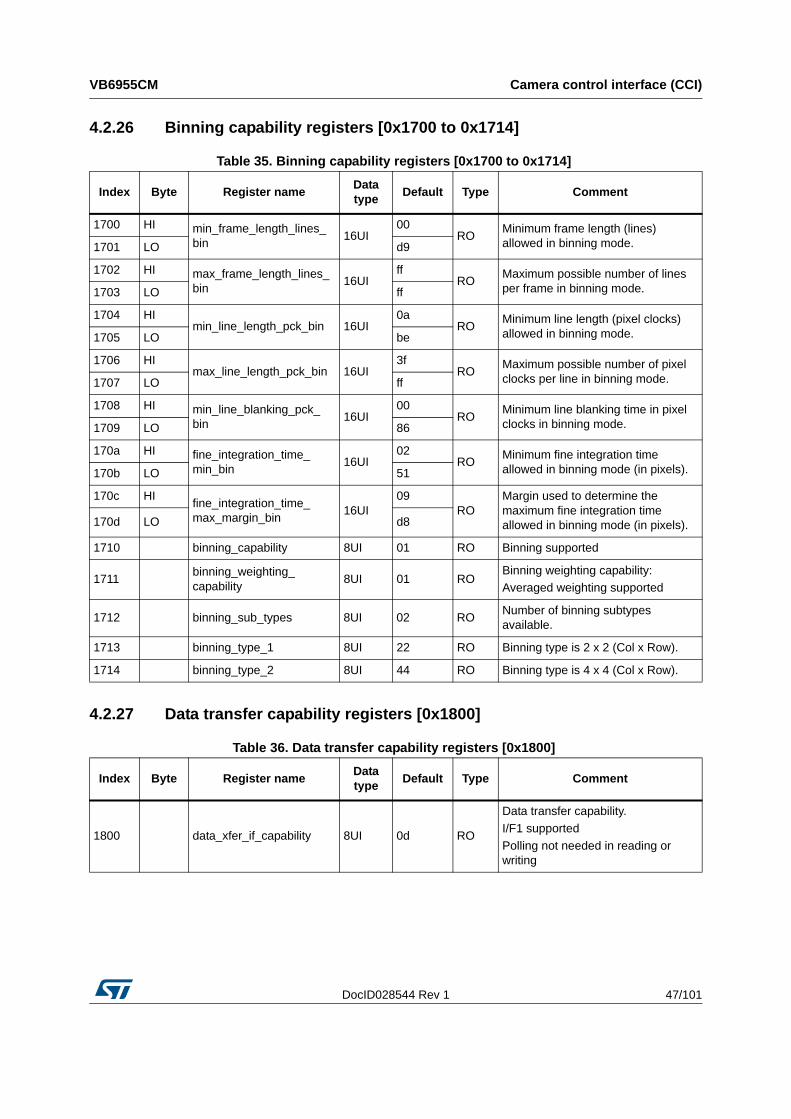
DocID028544 Rev 1 47/101
VB6955CM Camera control interface (CCI)
50
4.2.26 Binning capability registers [0x1700 to 0x1714]
4.2.27 Data transfer capability registers [0x1800]
Table 35. Binning capability registers [0x1700 to 0x1714]
Index Byte Register nameData type
Default Type Comment
1700 HI min_frame_length_lines_ bin
16UI00
ROMinimum frame length (lines) allowed in binning mode.1701 LO d9
1702 HI max_frame_length_lines_bin
16UIff
ROMaximum possible number of lines per frame in binning mode.1703 LO ff
1704 HImin_line_length_pck_bin 16UI
0aRO
Minimum line length (pixel clocks) allowed in binning mode.1705 LO be
1706 HImax_line_length_pck_bin 16UI
3fRO
Maximum possible number of pixel clocks per line in binning mode.1707 LO ff
1708 HI min_line_blanking_pck_ bin
16UI00
ROMinimum line blanking time in pixel clocks in binning mode.1709 LO 86
170a HI fine_integration_time_ min_bin
16UI02
ROMinimum fine integration time allowed in binning mode (in pixels).170b LO 51
170c HIfine_integration_time_ max_margin_bin
16UI09
ROMargin used to determine the maximum fine integration time allowed in binning mode (in pixels).170d LO d8
1710 binning_capability 8UI 01 RO Binning supported
1711binning_weighting_ capability
8UI 01 ROBinning weighting capability:
Averaged weighting supported
1712 binning_sub_types 8UI 02 RONumber of binning subtypes available.
1713 binning_type_1 8UI 22 RO Binning type is 2 x 2 (Col x Row).
1714 binning_type_2 8UI 44 RO Binning type is 4 x 4 (Col x Row).
Table 36. Data transfer capability registers [0x1800]
Index Byte Register nameData type
Default Type Comment
1800 data_xfer_if_capability 8UI 0d RO
Data transfer capability.
I/F1 supported
Polling not needed in reading or writing
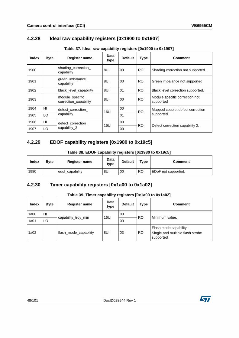
Camera control interface (CCI) VB6955CM
48/101 DocID028544 Rev 1
4.2.28 Ideal raw capability registers [0x1900 to 0x1907]
4.2.29 EDOF capability registers [0x1980 to 0x19c5]
4.2.30 Timer capability registers [0x1a00 to 0x1a02]
Table 37. Ideal raw capability registers [0x1900 to 0x1907]
Index Byte Register nameData type
Default Type Comment
1900shading_correction_ capability
8UI 00 RO Shading correction not supported.
1901green_imbalance_ capability
8UI 00 RO Green imbalance not supported
1902 black_level_capability 8UI 01 RO Black level correction supported.
1903module_specific_ correction_capability
8UI 00 ROModule specific correction not supported
1904 HI defect_correction_ capability
16UI00
ROMapped couplet defect correction supported.1905 LO 01
1906 HI defect_correction_ capability_2
16UI00
RO Defect correction capability 2.1907 LO 00
Table 38. EDOF capability registers [0x1980 to 0x19c5]
Index Byte Register nameData type
Default Type Comment
1980 edof_capability 8UI 00 RO EDoF not supported.
Table 39. Timer capability registers [0x1a00 to 0x1a02]
Index Byte Register nameData type
Default Type Comment
1a00 HIcapability_trdy_min 16UI
00RO Minimum value.
1a01 LO 00
1a02 flash_mode_capability 8UI 03 ROFlash mode capability:
Single and multiple flash strobe supported
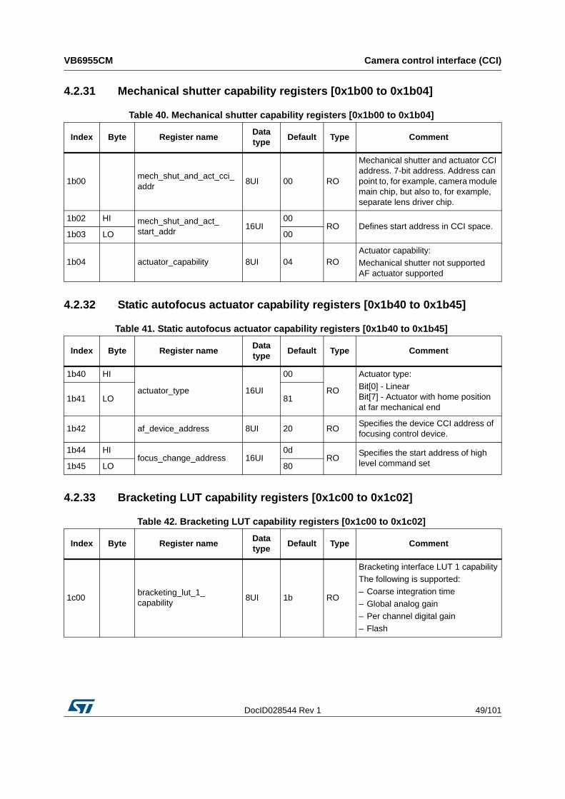
DocID028544 Rev 1 49/101
VB6955CM Camera control interface (CCI)
50
4.2.31 Mechanical shutter capability registers [0x1b00 to 0x1b04]
4.2.32 Static autofocus actuator capability registers [0x1b40 to 0x1b45]
4.2.33 Bracketing LUT capability registers [0x1c00 to 0x1c02]
Table 40. Mechanical shutter capability registers [0x1b00 to 0x1b04]
Index Byte Register nameData type
Default Type Comment
1b00mech_shut_and_act_cci_ addr
8UI 00 RO
Mechanical shutter and actuator CCI address. 7-bit address. Address can point to, for example, camera module main chip, but also to, for example, separate lens driver chip.
1b02 HI mech_shut_and_act_ start_addr
16UI00
RO Defines start address in CCI space.1b03 LO 00
1b04 actuator_capability 8UI 04 ROActuator capability:
Mechanical shutter not supported AF actuator supported
Table 41. Static autofocus actuator capability registers [0x1b40 to 0x1b45]
Index Byte Register nameData type
Default Type Comment
1b40 HI
actuator_type 16UI
00
RO
Actuator type:
Bit[0] - Linear Bit[7] - Actuator with home position at far mechanical end
1b41 LO 81
1b42 af_device_address 8UI 20 ROSpecifies the device CCI address of focusing control device.
1b44 HIfocus_change_address 16UI
0dRO
Specifies the start address of high level command set 1b45 LO 80
Table 42. Bracketing LUT capability registers [0x1c00 to 0x1c02]
Index Byte Register nameData type
Default Type Comment
1c00bracketing_lut_1_ capability
8UI 1b RO
Bracketing interface LUT 1 capability
The following is supported:
– Coarse integration time
– Global analog gain
– Per channel digital gain
– Flash
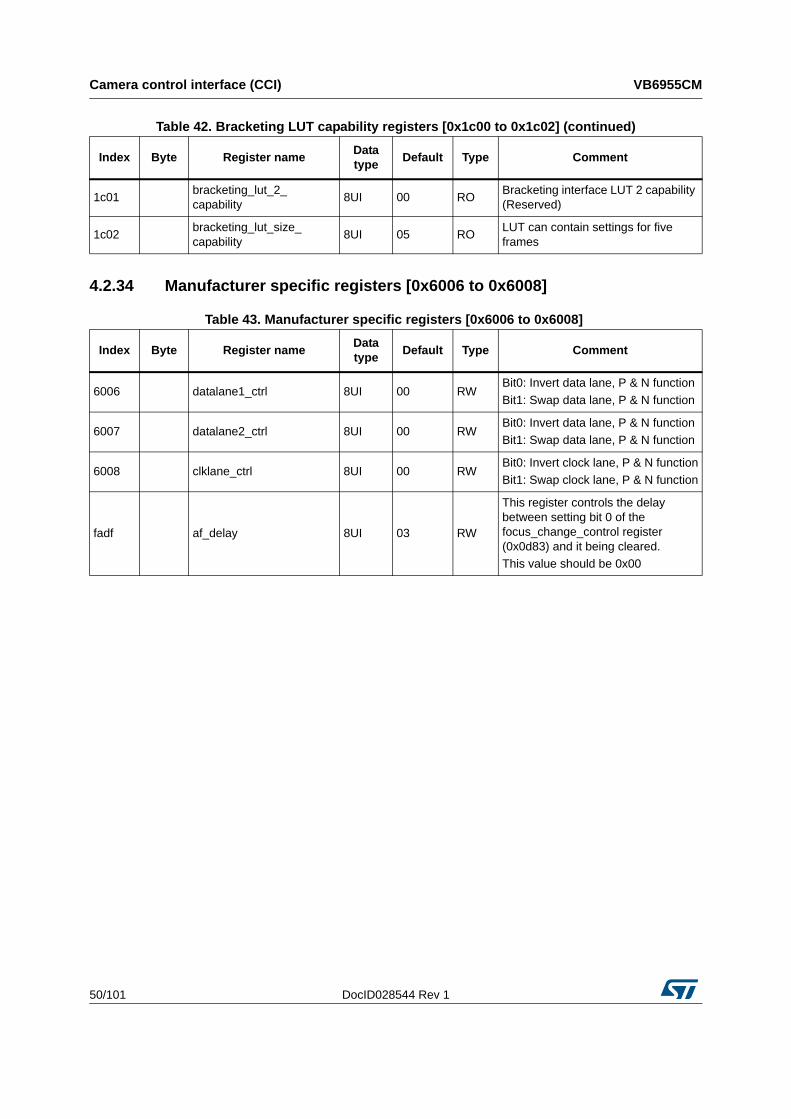
Camera control interface (CCI) VB6955CM
50/101 DocID028544 Rev 1
4.2.34 Manufacturer specific registers [0x6006 to 0x6008]
1c01bracketing_lut_2_ capability
8UI 00 ROBracketing interface LUT 2 capability (Reserved)
1c02bracketing_lut_size_ capability
8UI 05 ROLUT can contain settings for five frames
Table 42. Bracketing LUT capability registers [0x1c00 to 0x1c02] (continued)
Index Byte Register nameData type
Default Type Comment
Table 43. Manufacturer specific registers [0x6006 to 0x6008]
Index Byte Register nameData type
Default Type Comment
6006 datalane1_ctrl 8UI 00 RWBit0: Invert data lane, P & N function
Bit1: Swap data lane, P & N function
6007 datalane2_ctrl 8UI 00 RWBit0: Invert data lane, P & N function
Bit1: Swap data lane, P & N function
6008 clklane_ctrl 8UI 00 RWBit0: Invert clock lane, P & N function
Bit1: Swap clock lane, P & N function
fadf af_delay 8UI 03 RW
This register controls the delay between setting bit 0 of the focus_change_control register (0x0d83) and it being cleared.
This value should be 0x00
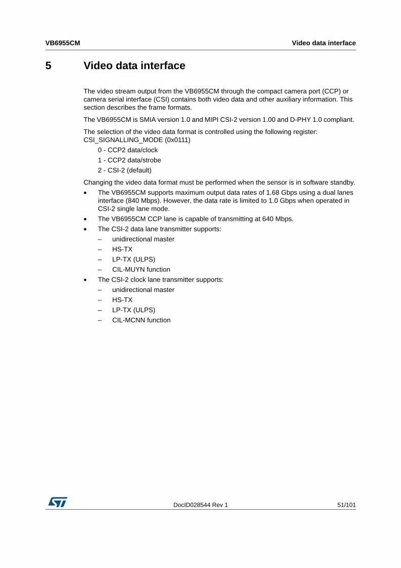
DocID028544 Rev 1 51/101
VB6955CM Video data interface
70
5 Video data interface
The video stream output from the VB6955CM through the compact camera port (CCP) or camera serial interface (CSI) contains both video data and other auxiliary information. This section describes the frame formats.
The VB6955CM is SMIA version 1.0 and MIPI CSI-2 version 1.00 and D-PHY 1.0 compliant.
The selection of the video data format is controlled using the following register: CSI_SIGNALLING_MODE (0x0111)
0 - CCP2 data/clock
1 - CCP2 data/strobe
2 - CSI-2 (default)
Changing the video data format must be performed when the sensor is in software standby.
• The VB6955CM supports maximum output data rates of 1.68 Gbps using a dual lanes interface (840 Mbps). However, the data rate is limited to 1.0 Gbps when operated in CSI-2 single lane mode.
• The VB6955CM CCP lane is capable of transmitting at 640 Mbps.
• The CSI-2 data lane transmitter supports:
– unidirectional master
– HS-TX
– LP-TX (ULPS)
– CIL-MUYN function
• The CSI-2 clock lane transmitter supports:
– unidirectional master
– HS-TX
– LP-TX (ULPS)
– CIL-MCNN function
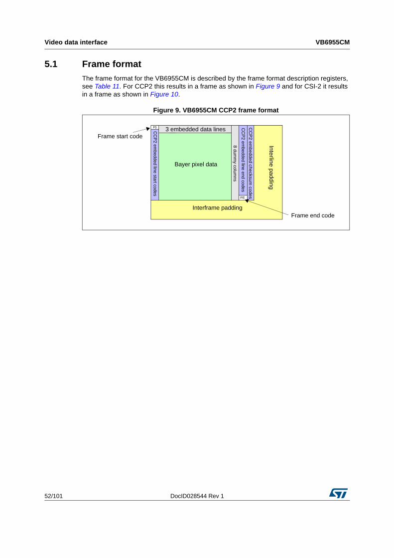
Video data interface VB6955CM
52/101 DocID028544 Rev 1
5.1 Frame format
The frame format for the VB6955CM is described by the frame format description registers, see Table 11. For CCP2 this results in a frame as shown in Figure 9 and for CSI-2 it results in a frame as shown in Figure 10.
Figure 9. VB6955CM CCP2 frame format
Inte
rline pa
dding
Interframe padding
Bayer pixel data
CC
P2 em
bedded line start codes
CC
P2
emb
ed
ded
checksu
m co
de
s
CC
P2 em
bedded line end codes
FE
FS 3 embedded data linesFrame start code
Frame end code
8 dumm
y columns
DocID028544 Rev 1 53/101
VB6955CM Video data interface
70
Figure 10. VB6955CM CSI-2 frame format
Embedded data lines
The embedded data lines provide a mechanism to embed non-image data such as sensor configuration details within the output data stream. The number of embedded data lines at the start and end of the frame is specified as part of the frame format description. VB6955CM has three embedded data lines.
Dummy pixel data
This is invalid pixel data. The receiver should always ignore dummy pixel data. The VB6955CM has eight dummy columns.
Bayer pixeldata
Embedded data
Frame start packet
Frame end packet
Lineblanking
Pac
ket f
oote
r (P
F)
Pac
ket h
ead
er (
PH
)
Frameblanking
FE
FS
Video data interface VB6955CM
54/101 DocID028544 Rev 1
Visible pixel data
The visible pixels contain valid image data.The correct integration time and analog gain for the visible pixels is specified in the blank lines at the start of the frame.The number of visible pixels can be varied with the requested frame size.
Dark pixel data (light shielded pixels)
The VB6955CM has 0 dark pixels.
Black pixel data (zero integration time)
The VB6955CM has 0 black pixels.
Manufacturer specific pixel data
The VB6955CM has 0 manufacturer specific pixels.
Interline padding/line blanking
During interline padding all bits in the data stream in a CCP2 frame are set to 1.
In a CSI-2 frame there is no concept of line blanking being transmitted, the sensor simply spends a longer time in the LP state between active line data.
Interframe padding/frame blanking
During interframe padding all bits in the data stream in a CCP2 frame are set to 1.
In a CSI-2 frame there is no concept of frame blanking being transmitted, the sensor simply spends a longer time in the LP state at the end of the active data for a frame.
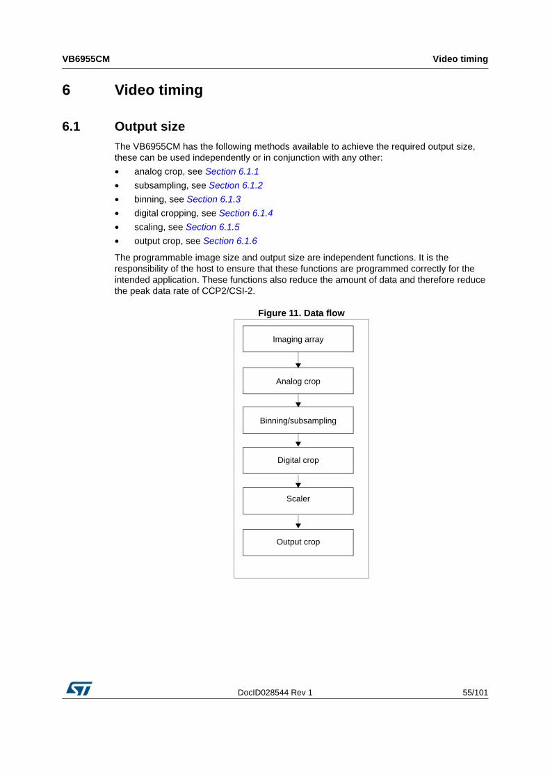
DocID028544 Rev 1 55/101
VB6955CM Video timing
70
6 Video timing
6.1 Output size
The VB6955CM has the following methods available to achieve the required output size, these can be used independently or in conjunction with any other:
• analog crop, see Section 6.1.1
• subsampling, see Section 6.1.2
• binning, see Section 6.1.3
• digital cropping, see Section 6.1.4
• scaling, see Section 6.1.5
• output crop, see Section 6.1.6
The programmable image size and output size are independent functions. It is the responsibility of the host to ensure that these functions are programmed correctly for the intended application. These functions also reduce the amount of data and therefore reduce the peak data rate of CCP2/CSI-2.
Figure 11. Data flow
Digital crop
Analog crop
Binning/subsampling
Imaging array
Scaler
Output crop
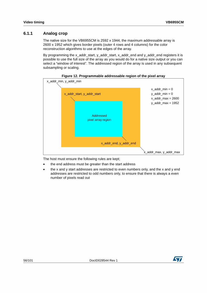
Video timing VB6955CM
56/101 DocID028544 Rev 1
6.1.1 Analog crop
The native size for the VB6955CM is 2592 x 1944, the maximum addressable array is 2600 x 1952 which gives border pixels (outer 4 rows and 4 columns) for the color reconstruction algorithms to use at the edges of the array.
By programming the x_addr_start, y_addr_start, x_addr_end and y_addr_end registers it is possible to use the full size of the array as you would do for a native size output or you can select a “window of interest”. The addressed region of the array is used in any subsequent subsampling or scaling.
Figure 12. Programmable addressable region of the pixel array
The host must ensure the following rules are kept;
• the end address must be greater than the start address
• the x and y start addresses are restricted to even numbers only, and the x and y end addresses are restricted to odd numbers only, to ensure that there is always a even number of pixels read out
y_addr_max = 1952
x_addr_max = 2600
y_addr_min = 0
x_addr_min = 0
x_addr_max, y_addr_max
x_addr_end, y_addr_end
Addressedpixel array region
x_addr_start, y_addr_start
x_addr_min, y_addr_min
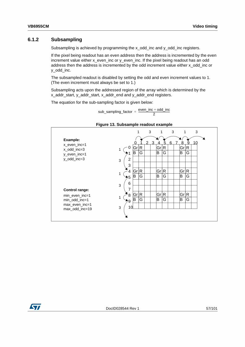
DocID028544 Rev 1 57/101
VB6955CM Video timing
70
6.1.2 Subsampling
Subsampling is achieved by programming the x_odd_inc and y_odd_inc registers.
If the pixel being readout has an even address then the address is incremented by the even increment value either x_even_inc or y_even_inc. If the pixel being readout has an odd address then the address is incremented by the odd increment value either x_odd_inc or y_odd_inc.
The subsampled readout is disabled by setting the odd and even increment values to 1. (The even increment must always be set to 1.)
Subsampling acts upon the addressed region of the array which is determined by the x_addr_start, y_addr_start, x_addr_end and y_addr_end registers.
The equation for the sub-sampling factor is given below:
Figure 13. Subsample readout example
sub_sampling_factoreven_inc odd_inc+
2---------------------------------------------------=
8
5
6
7
GGr RB
GGr RB
GGr RB
GGr RB
GGr RB
GGr RB
GGr RB
GGr RB
GGr RB
4
1
2
3
9
10
85 6 74 1 2 3 90 100
1 1 13 3 3
1
1
1
3
3
3
Example:x_even_inc=1x_odd_inc=3y_even_inc=1y_odd_inc=3
Control range:
min_even_inc=1min_odd_inc=1max_even_inc=1max_odd_inc=19
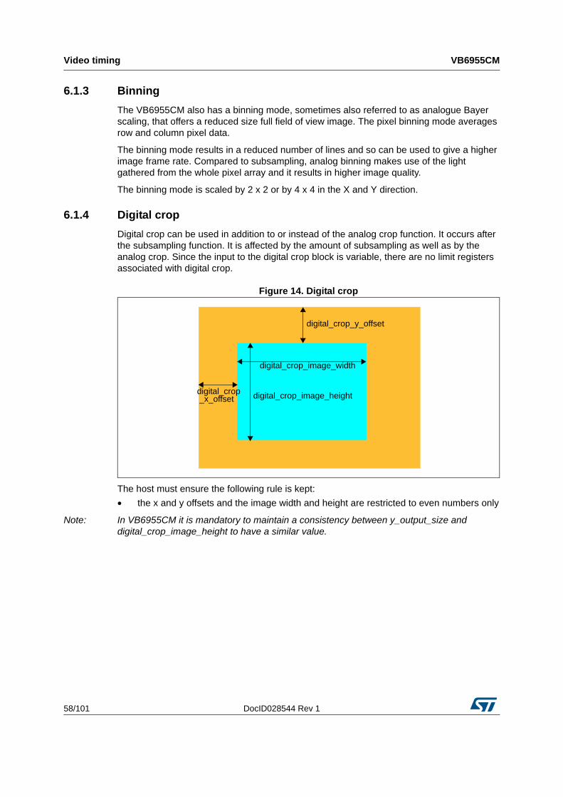
Video timing VB6955CM
58/101 DocID028544 Rev 1
6.1.3 Binning
The VB6955CM also has a binning mode, sometimes also referred to as analogue Bayer scaling, that offers a reduced size full field of view image. The pixel binning mode averages row and column pixel data.
The binning mode results in a reduced number of lines and so can be used to give a higher image frame rate. Compared to subsampling, analog binning makes use of the light gathered from the whole pixel array and it results in higher image quality.
The binning mode is scaled by 2 x 2 or by 4 x 4 in the X and Y direction.
6.1.4 Digital crop
Digital crop can be used in addition to or instead of the analog crop function. It occurs after the subsampling function. It is affected by the amount of subsampling as well as by the analog crop. Since the input to the digital crop block is variable, there are no limit registers associated with digital crop.
Figure 14. Digital crop
The host must ensure the following rule is kept:
• the x and y offsets and the image width and height are restricted to even numbers only
Note: In VB6955CM it is mandatory to maintain a consistency between y_output_size and digital_crop_image_height to have a similar value.
digital_crop_image_height
digital_crop_image_width
digital_crop_y_offset
digital_crop_x_offset
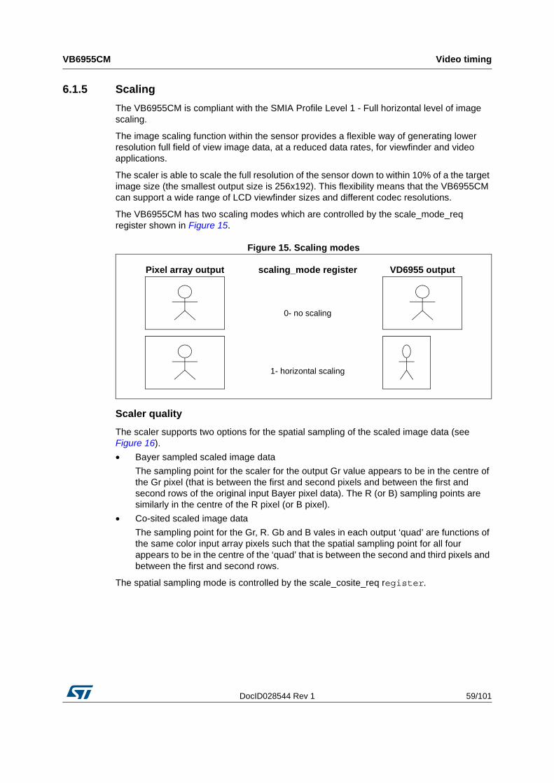
DocID028544 Rev 1 59/101
VB6955CM Video timing
70
6.1.5 Scaling
The VB6955CM is compliant with the SMIA Profile Level 1 - Full horizontal level of image scaling.
The image scaling function within the sensor provides a flexible way of generating lower resolution full field of view image data, at a reduced data rates, for viewfinder and video applications.
The scaler is able to scale the full resolution of the sensor down to within 10% of a the target image size (the smallest output size is 256x192). This flexibility means that the VB6955CM can support a wide range of LCD viewfinder sizes and different codec resolutions.
The VB6955CM has two scaling modes which are controlled by the scale_mode_req register shown in Figure 15.
Figure 15. Scaling modes
Scaler quality
The scaler supports two options for the spatial sampling of the scaled image data (see Figure 16).
• Bayer sampled scaled image data
The sampling point for the scaler for the output Gr value appears to be in the centre of the Gr pixel (that is between the first and second pixels and between the first and second rows of the original input Bayer pixel data). The R (or B) sampling points are similarly in the centre of the R pixel (or B pixel).
• Co-sited scaled image data
The sampling point for the Gr, R. Gb and B vales in each output ‘quad’ are functions of the same color input array pixels such that the spatial sampling point for all four appears to be in the centre of the ‘quad’ that is between the second and third pixels and between the first and second rows.
The spatial sampling mode is controlled by the scale_cosite_req register.
Pixel array output scaling_mode register VD6955 output
0- no scaling
1- horizontal scaling
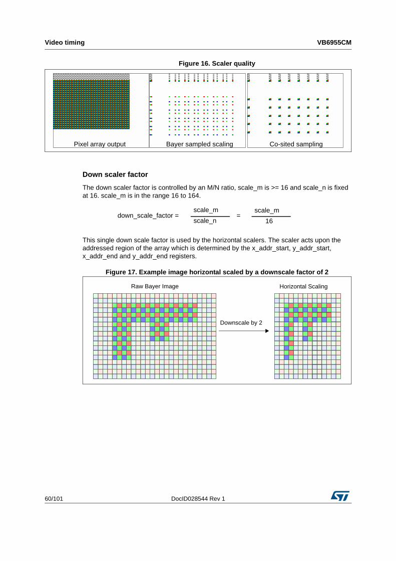
Video timing VB6955CM
60/101 DocID028544 Rev 1
Figure 16. Scaler quality
Down scaler factor
The down scaler factor is controlled by an M/N ratio, scale_m is >= 16 and scale_n is fixed at 16. scale_m is in the range 16 to 164.
This single down scale factor is used by the horizontal scalers. The scaler acts upon the addressed region of the array which is determined by the x_addr_start, y_addr_start, x_addr_end and y_addr_end registers.
Figure 17. Example image horizontal scaled by a downscale factor of 2
Pixel array output Bayer sampled scaling Co-sited sampling
down_scale_factor =scale_m scale_m
scale_n 16=
Raw Bayer Image
Downscale by 2
Horizontal Scaling
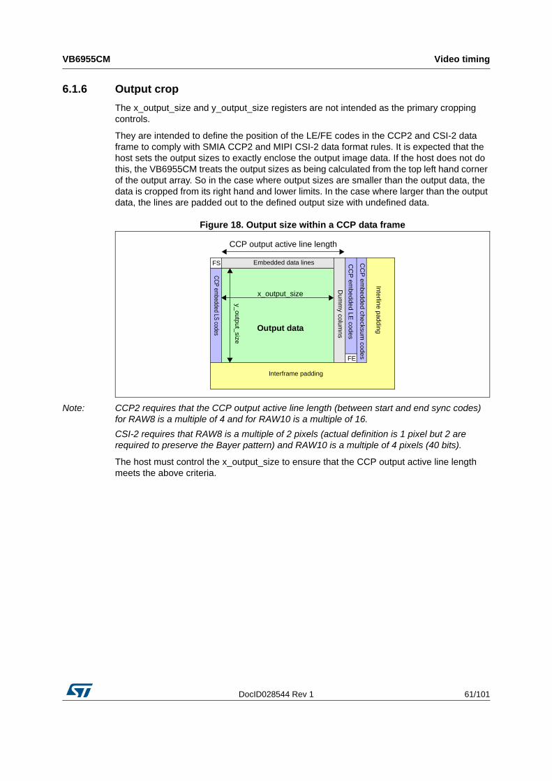
DocID028544 Rev 1 61/101
VB6955CM Video timing
70
6.1.6 Output crop
The x_output_size and y_output_size registers are not intended as the primary cropping controls.
They are intended to define the position of the LE/FE codes in the CCP2 and CSI-2 data frame to comply with SMIA CCP2 and MIPI CSI-2 data format rules. It is expected that the host sets the output sizes to exactly enclose the output image data. If the host does not do this, the VB6955CM treats the output sizes as being calculated from the top left hand corner of the output array. So in the case where output sizes are smaller than the output data, the data is cropped from its right hand and lower limits. In the case where larger than the output data, the lines are padded out to the defined output size with undefined data.
Figure 18. Output size within a CCP data frame
Note: CCP2 requires that the CCP output active line length (between start and end sync codes) for RAW8 is a multiple of 4 and for RAW10 is a multiple of 16.
CSI-2 requires that RAW8 is a multiple of 2 pixels (actual definition is 1 pixel but 2 are required to preserve the Bayer pattern) and RAW10 is a multiple of 4 pixels (40 bits).
The host must control the x_output_size to ensure that the CCP output active line length meets the above criteria.
CCP output active line length
Inte
rline
pad
ding
Interframe padding
x_output_size
y_ou
tpu
t_size
Output dataC
CP em
bedded LS codes
CC
P e
mb
ed
ded
che
cksum co
des
CC
P e
mb
ed
ded
LE
cod
es
FE
FS Embedded data lines
Du
mm
y colum
ns
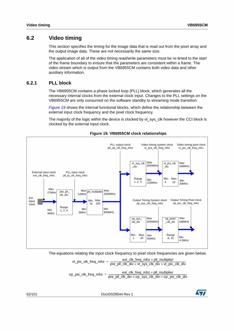
Video timing VB6955CM
62/101 DocID028544 Rev 1
6.2 Video timing
This section specifies the timing for the image data that is read out from the pixel array and the output image data. These are not necessarily the same size.
The application of all of the video timing read/write parameters must be re-timed to the start of the frame boundary to ensure that the parameters are consistent within a frame. The video stream which is output from the VB6955CM contains both video data and other auxiliary information.
6.2.1 PLL block
The VB6955CM contains a phase locked loop (PLL) block, which generates all the necessary internal clocks from the external clock input. Changes to the PLL settings on the VB6955CM are only consumed on the software standby to streaming mode transition.
Figure 19 shows the internal functional blocks, which define the relationship between the external input clock frequency and the pixel clock frequency.
The majority of the logic within the device is clocked by vt_sys_clk however the CCI block is clocked by the external input clock.
Figure 19. VB6955CM clock relationships
The equations relating the input clock frequency to pixel clock frequencies are given below.
Min.76
Max.332
pll_multiplierpre_pll_clk_div
Range1, 2, 4
Ext. input clock
External input clockext_clk_freq_mhz
PLL input clockpll_ip_clk_freq_mhz
PLL output clockpll_op_clk_freq_mhz
Video timing pixel clockvt_pix_clk_freq_mhz
Video timing system clockvt_sys_clk_freq_mhz
Range1, 2, 4
vt_sys_clk_div
vt_pix_clk_div
Min.4
Max.10
Output Timing System clockop_sys_clk_freq_mhz
Output Timing Pixel clockop_pix_clk_freq_mhz
op_pixel_clk_div
op_sys_clk_div
Min.1
Max.20
Range6, 10
Max27MHz
6MHzMin Min Min
Min Min
MinMin
MaxMax
MaxMax
MaxMax
2000MHz 168MHz
30MHz225MHz
4.5MHz
168MHz2000MHz
45MHz
900MHz
2000MHz
6MHz
12MHz
vt_pix_clk_freq_mhzext_clk_freq_mhz pll_multiplier×
pre_pll_clk_div vt_sys_clk_div vt_pix_clk_div××--------------------------------------------------------------------------------------------------------------------------------=
op_pix_clk_freq_mhzext_clk_freq_mhz pll_multiplier×
pre_pll_clk_div op_sys_clk_div op_pix_clk_div××-------------------------------------------------------------------------------------------------------------------------------------=
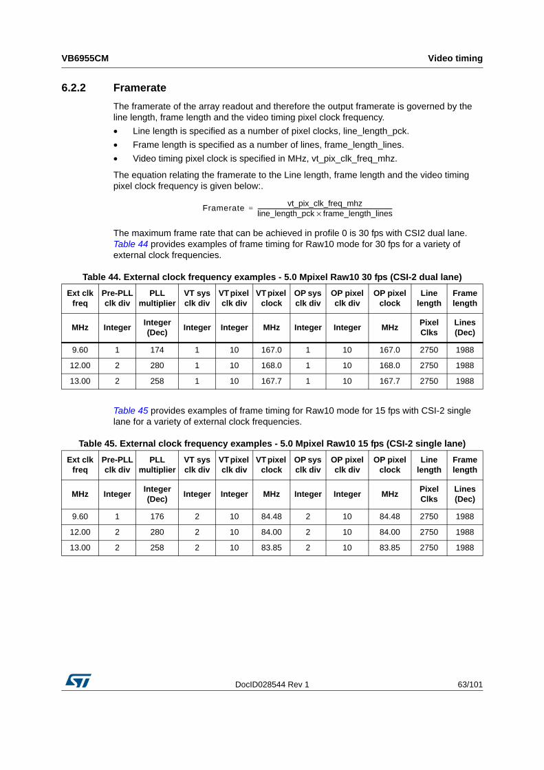
DocID028544 Rev 1 63/101
VB6955CM Video timing
70
6.2.2 Framerate
The framerate of the array readout and therefore the output framerate is governed by the line length, frame length and the video timing pixel clock frequency.
• Line length is specified as a number of pixel clocks, line_length_pck.
• Frame length is specified as a number of lines, frame_length_lines.
• Video timing pixel clock is specified in MHz, vt_pix_clk_freq_mhz.
The equation relating the framerate to the Line length, frame length and the video timing pixel clock frequency is given below:.
The maximum frame rate that can be achieved in profile 0 is 30 fps with CSI2 dual lane. Table 44 provides examples of frame timing for Raw10 mode for 30 fps for a variety of external clock frequencies.
Table 45 provides examples of frame timing for Raw10 mode for 15 fps with CSI-2 single lane for a variety of external clock frequencies.
Frameratevt_pix_clk_freq_mhz
line_length_pck frame_length_lines×--------------------------------------------------------------------------------------------------=
Table 44. External clock frequency examples - 5.0 Mpixel Raw10 30 fps (CSI-2 dual lane)
Ext clk freq
Pre-PLL clk div
PLL multiplier
VT sys clk div
VT pixel clk div
VT pixel clock
OP sys clk div
OP pixel clk div
OP pixel clock
Line length
Frame length
MHz IntegerInteger (Dec)
Integer Integer MHz Integer Integer MHzPixel Clks
Lines (Dec)
9.60 1 174 1 10 167.0 1 10 167.0 2750 1988
12.00 2 280 1 10 168.0 1 10 168.0 2750 1988
13.00 2 258 1 10 167.7 1 10 167.7 2750 1988
Table 45. External clock frequency examples - 5.0 Mpixel Raw10 15 fps (CSI-2 single lane)
Ext clk freq
Pre-PLL clk div
PLL multiplier
VT sys clk div
VT pixel clk div
VT pixel clock
OP sys clk div
OP pixel clk div
OP pixel clock
Line length
Frame length
MHz IntegerInteger (Dec)
Integer Integer MHz Integer Integer MHzPixel Clks
Lines (Dec)
9.60 1 176 2 10 84.48 2 10 84.48 2750 1988
12.00 2 280 2 10 84.00 2 10 84.00 2750 1988
13.00 2 258 2 10 83.85 2 10 83.85 2750 1988
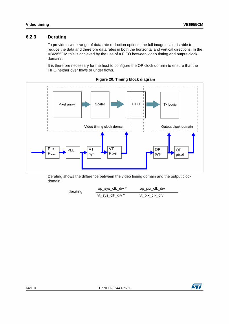
Video timing VB6955CM
64/101 DocID028544 Rev 1
6.2.3 Derating
To provide a wide range of data rate reduction options, the full image scaler is able to reduce the data and therefore data rates in both the horizontal and vertical directions. In the VB6955CM this is achieved by the use of a FIFO between video timing and output clock domains.
It is therefore necessary for the host to configure the OP clock domain to ensure that the FIFO neither over flows or under flows.
Figure 20. Timing block diagram
Derating shows the difference between the video timing domain and the output clock domain.
Pre PLL
PLL VT sys
VT Pixel
OP sys
OP pixel
Pixel array Scaler FIFO
Tx Logic
Output clock domainVideo timing clock domain
derating =vt_sys_clk_div *
op_pix_clk_divop_sys_clk_div *
vt_pix_clk_div
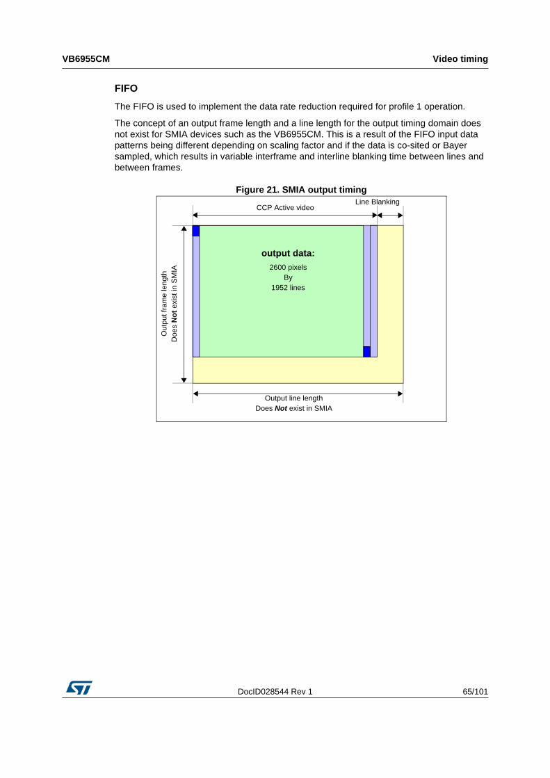
DocID028544 Rev 1 65/101
VB6955CM Video timing
70
FIFO
The FIFO is used to implement the data rate reduction required for profile 1 operation.
The concept of an output frame length and a line length for the output timing domain does not exist for SMIA devices such as the VB6955CM. This is a result of the FIFO input data patterns being different depending on scaling factor and if the data is co-sited or Bayer sampled, which results in variable interframe and interline blanking time between lines and between frames.
Figure 21. SMIA output timing
output data:
CCP Active video
2600 pixelsBy
1952 lines
Line Blanking
Out
put f
ram
e le
ngt
hD
oes
No
t ex
ist i
n S
MIA
Output line lengthDoes Not exist in SMIA
Video timing VB6955CM
66/101 DocID028544 Rev 1
6.3 Image and video size capabilities
The VB6955CM supports various video modes ranging from VGA@120 fps to HD formats like 3.8 Mpixel @ 42 fps, 1080p30 and 720p30.
The VB6955CM has two CSI-2 data lanes capable of transmitting up to:
• 1.68 Gbps in dual lane mode (840 Mbps per lane)
• 1.0 Gbps in single lane mode
6.4 Bayer pattern
The three color (Red, Green, Blue) filters are arranged over the pixel array in a repeated 2 x 2 arrangement known as the Bayer Pattern. When the pixel array is read, the output order of red, green, blue depends on the settings of vertical flip and horizontal mirror.
Figure 22 shows the read-out order for the default settings of vertical flip and horizontal mirror both turned off. Vertical flip changes the first line to be output from a green/red line to a blue/green line and horizontal mirror changes the sequence within a line, for example, green/red to red/green.
As shown in Figure 22, the first pixel to be readout from the imaging array is green followed by red.
Table 46. Examples of video mode capabilities
Resolution FPS Mode FormatNumber of
CSI2 interfaces
Lane data rate (Mbps)
Full FOV2600 x 1952 23 (max) 5 Mpixel 4:3 RAW8, 10/8 1 lane 996
2600 x 1952 31 (max) 5 Mpixel 4:3 RAW10 2 lanes 840
HD video capture
1080p 41 (max)16:9 (full horizontal + vertical crop)
RAW8, 10/8 1 lane 996
1080p 55 (max)16:9 (full horizontal + vertical crop)
RAW8, 10/8 2 lanes 672
1080p 33 (max)16:9 (full horizontal + vertical crop)
RAW10 1 lane 996
1080p 55 (max)16:9 (full horizontal + vertical crop)
RAW10 2 lanes 840
720p 61 (max)3.8 Mpixel 16:9 + Binning 2x2
RAW8, 10/8 1 lane 996
720p 82 (max)3.8 Mpixel 16:9 + Binning 2x2
RAW10 2 lanes 840
VGA
VGA (648x488) 895 Mpixel 4:3 with Binning 2x2 + 2x2 subsampling
RAW8, 10/8 1 lane 996
VGA (648x488) 1205 Mpixel 4:3 with Binning 2x2 + 2x2 subsampling
RAW8, 10/8 2 lanes 672
VGA (648x488) 1205 Mpixel 4:3 with Binning 2x2 + 2x2 subsampling
RAW10 2 lanes 840
WVGA WVGA (800x480) 120 1.5 Mpixel + Binning 2x2 RAW10 2 lanes 840
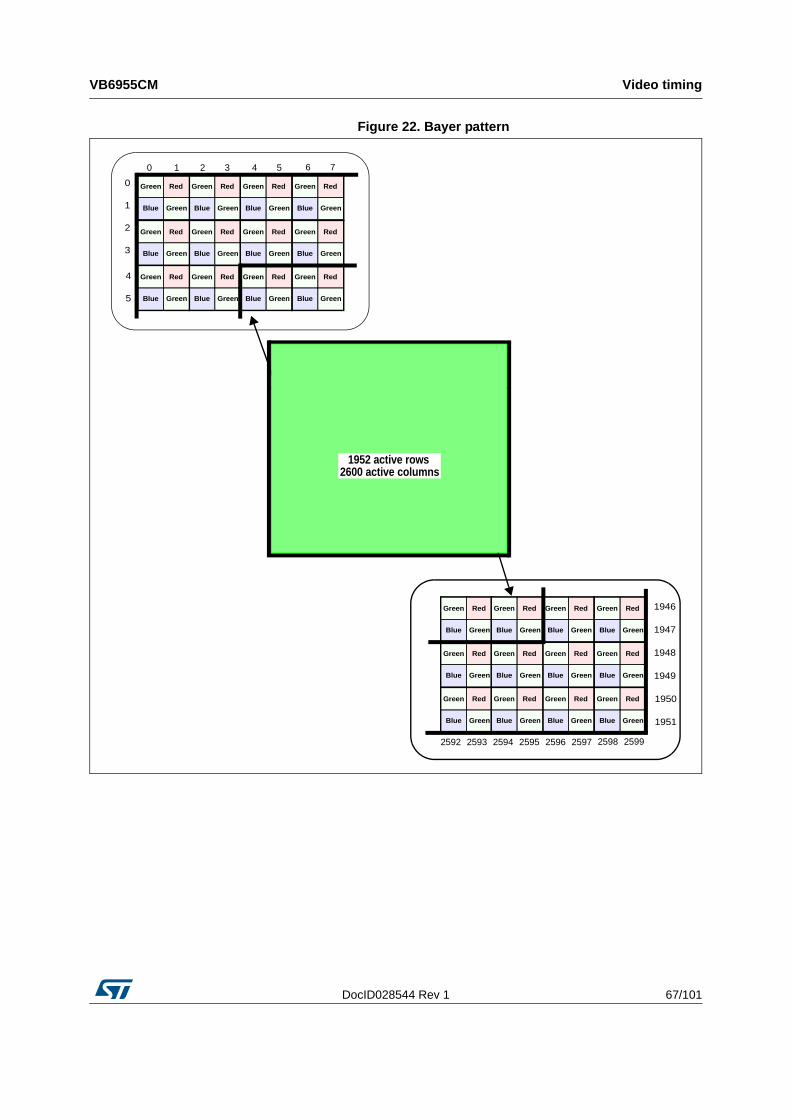
DocID028544 Rev 1 67/101
VB6955CM Video timing
70
Figure 22. Bayer pattern
Blue Green
Green Red
Blue Green
Green Red
3210
1
3
2
0
54
Blue Green
Green Red
5
4
76
2595259425932592
1947
1949
1948
1946
25972596
1951
1950
25992598
Blue Green
Green Red
Blue Green
Green Red
Blue Green
Green Red
Blue Green
Green Red
Blue Green
Green Red
Blue Green
Green Red
Blue Green
Green Red
Blue Green
Green Red
Blue Green
Green Red
Blue Green
Green Red
Blue Green
Green Red
Blue Green
Green Red
Blue Green
Green Red
Blue Green
Green Red
Blue Green
Green Red
Blue Green
Green Red
Blue Green
Green Red
Blue Green
Green Red
Blue Green
Green Red
Blue Green
Green Red
Blue Green
Green Red
1952 active rows2600 active columns
Video timing VB6955CM
68/101 DocID028544 Rev 1
6.5 Image compression
The objective of image compression is to reduce the required bandwidth in transmission between the sensor and the host.
The key features of the DPCM/PCM compression algorithm are:
• visually lossless
• low cost implementation (no line memories are required)
• fixed rate compression
The 10-bit to 8-bit DPCM/PCM image compression algorithm is supported by VB6955CM. 10-bit to 8-bit compression has the additional advantage that one pixel value equals one byte of data.
The level of compression is controlled through the CSI_data_format register. The same register is also used to enable and disable compression.
The compression_mode register is used to select which compression algorithm is used. Currently only the DPCM/PCM technique is supported. Therefore the value of this register is always 0x01.
The compression_capability register tells the host whether a sensor does or does not have compression and if it has compression then what is the compression technique. Currently only the DPCM/PCM technique is supported.
Also refer to section 10 of the SMIA1.0 specification document.
6.6 Exposure and gain control
VB6955CM does not contain any form of automatic exposure control. To produce a correctly exposed image the integration period and analogue gain for the pixels must be calculated by an exposure control algorithm implemented externally. The parameters are then written to the VB6955CM through the CCI interface.
The exposure control parameters available on VB6955CM are:
• fine integration time
• coarse integration time
• analog gain
• digital gain
The exposure control parameter registers are defined in Section 4.2.6.
Integration time and analogue gain capability registers should be used to determine the exposure control parameter limits for a given video timing configuration. See Section 6.7 of the SMIA 1.0 part 1 specification for more information on how to interpret the integration and gain capability registers and how to calculate exposure and gain limits.
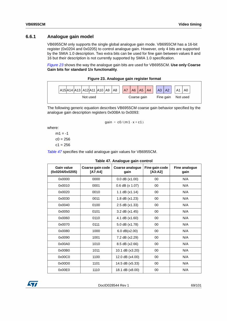
DocID028544 Rev 1 69/101
VB6955CM Video timing
70
6.6.1 Analogue gain model
VB6955CM only supports the single global analogue gain mode. VB6955CM has a 16-bit register (0x0204 and 0x0205) to control analogue gain. However, only 4 bits are supported by the SMIA 1.0 description. Two extra bits can be used for fine gain between values 8 and 16 but their description is not currently supported by SMIA 1.0 specification.
Figure 23 shows the way the analogue gain bits are used for VB6955CM. Use only Coarse Gain bits for standard 1/x functionality.
Figure 23. Analogue gain register format
The following generic equation describes VB6955CM coarse gain behavior specified by the analogue gain description registers 0x008A to 0x0093:
where:
m1 = -1
c0 = 256
c1 = 256
Table 47 specifies the valid analogue gain values for VB6955CM.
Table 47. Analogue gain control
Gain value (0x0204/0x0205)
Coarse gain code [A7:A4]
Coarse analogue gain
Fine gain code [A3:A2]
Fine analogue gain
0x0000 0000 0.0 dB (x1.00) 00 N/A
0x0010 0001 0.6 dB (x 1.07) 00 N/A
0x0020 0010 1.1 dB (x1.14) 00 N/A
0x0030 0011 1.8 dB (x1.23) 00 N/A
0x0040 0100 2.5 dB (x1.33) 00 N/A
0x0050 0101 3.2 dB (x1.45) 00 N/A
0x0060 0110 4.1 dB (x1.60) 00 N/A
0x0070 0111 5.0 dB (x1.78) 00 N/A
0x0080 1000 6.0 dB(x2.00) 00 N/A
0x0090 1001 7.2 dB (x2.29) 00 N/A
0x00A0 1010 8.5 dB (x2.66) 00 N/A
0x00B0 1011 10.1 dB (x3.20) 00 N/A
0x00C0 1100 12.0 dB (x4.00) 00 N/A
0x00D0 1101 14.5 dB (x5.33) 00 N/A
0x00E0 1110 18.1 dB (x8.00) 00 N/A
A7 A6 A5 A4 A3 A1 A0A8A9A15 A14 A13 A12 A11 A10 A2
Coarse gain Fine gain Not usedNot used
gain c0 m( 1 x⋅⁄ c1 )+=
Video timing VB6955CM
70/101 DocID028544 Rev 1
Also refer to section 6.3 of the SMIA1.0 specification document.
6.6.2 Digital gain
To help compensate for the relatively coarse analogue gain steps, VB6955CM contains a digital multiplier to “fill” in the missing steps. By mixing analogue and digital gain it is possible to implement 3% gain steps across the full 1x to 16x gain range
The details of the digital gain implementation are listed below:
• four individual 16-bit digital channel gains - one per Bayer channel
– digital_gain_greenR (0x020E and 0x020F)
– digital_gain_red (0x0210 and 0x0211)
– digital_gain_blue (0x0212 and 0x0213)
– digital_gain_greenB (0x0214 and 0x0215)
• the digital gain range for each channel is 1.000 to 1.96875 in steps of 0.03125 (1/32), that is, 5 fractional bits
– digital_gain_min {0x1084:0x1085} = 0x0100 (1.00)
– digital_gain_max {0x1086:0x1087} = 0x01F8 (1.96875)
– digital_gain_step {0x1088:0x1089} = 0x0008 (0.03125)
6.6.3 Integration and gain parameter re-timing
The modification of exposure parameter (integration time, analog and digital gain) register values does not take effect immediately.
The exact time at which changes to certain parameters take effect is controlled both to ensure that each frame of image data produced has consistent settings and that changes in groups of related parameters can be synchronized.
A group of parameter changes is marked by the host using a dedicated Boolean control parameter, grouped_parameter_hold (register 0x0104). Any changes made to ‘retimed’ parameters while the grouped_parameter_hold signal is in the ‘hold’ state will be considered part of the same group. Only when the grouped_parameter_hold control signal is moved back to the default ‘no-hold’ state will the group of changes be executed.
0x00E4 1110 fine ctrl 01 19.2 dB (x9.14)
0x00E8 1110 fine ctrl 10 20.6 dB (x10.66)
0x00EC 1110 fine ctrl 11 22.1 dB (x12.80)
0x00F0 1111 24.1 dB (x16.00) 00 N/A
Table 47. Analogue gain control (continued)
Gain value (0x0204/0x0205)
Coarse gain code [A7:A4]
Coarse analogue gain
Fine gain code [A3:A2]
Fine analogue gain
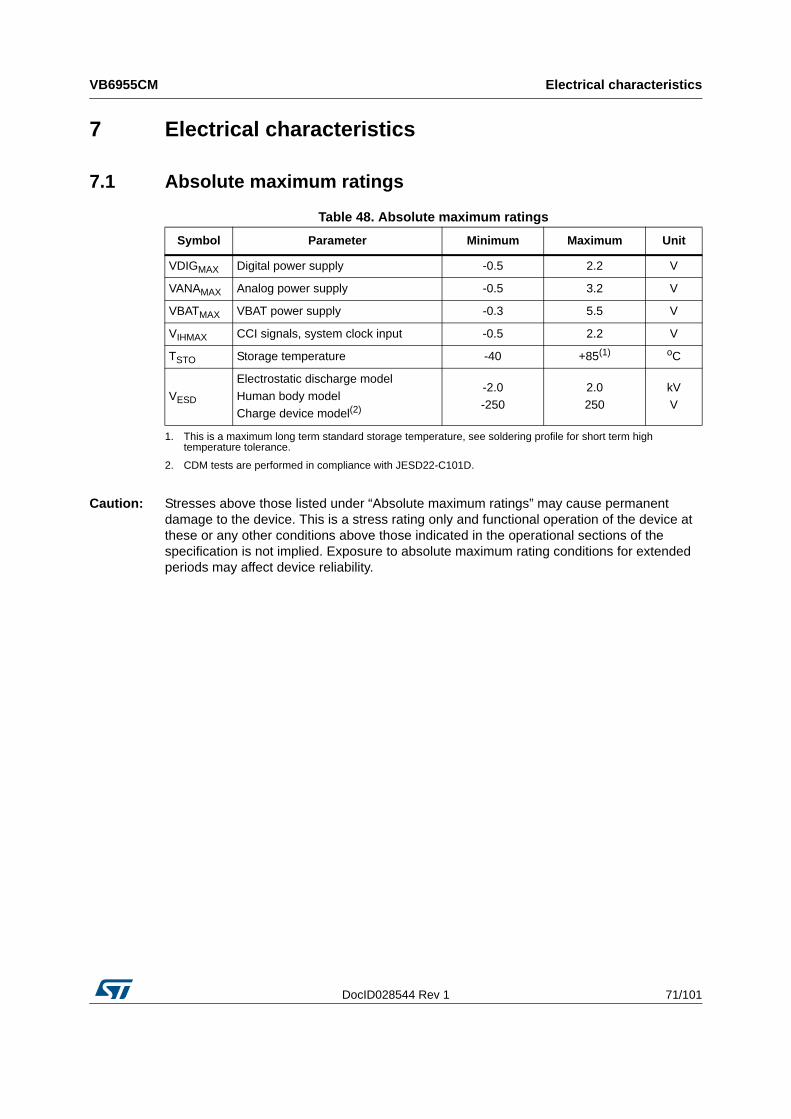
DocID028544 Rev 1 71/101
VB6955CM Electrical characteristics
76
7 Electrical characteristics
7.1 Absolute maximum ratings
Caution: Stresses above those listed under “Absolute maximum ratings” may cause permanent damage to the device. This is a stress rating only and functional operation of the device at these or any other conditions above those indicated in the operational sections of the specification is not implied. Exposure to absolute maximum rating conditions for extended periods may affect device reliability.
Table 48. Absolute maximum ratings
Symbol Parameter Minimum Maximum Unit
VDIGMAX Digital power supply -0.5 2.2 V
VANAMAX Analog power supply -0.5 3.2 V
VBATMAX VBAT power supply -0.3 5.5 V
VIHMAX CCI signals, system clock input -0.5 2.2 V
TSTO Storage temperature -40 +85(1)
1. This is a maximum long term standard storage temperature, see soldering profile for short term high temperature tolerance.
oC
VESD
Electrostatic discharge model
Human body model
Charge device model(2)
2. CDM tests are performed in compliance with JESD22-C101D.
-2.0
-250
2.0
250
kV
V
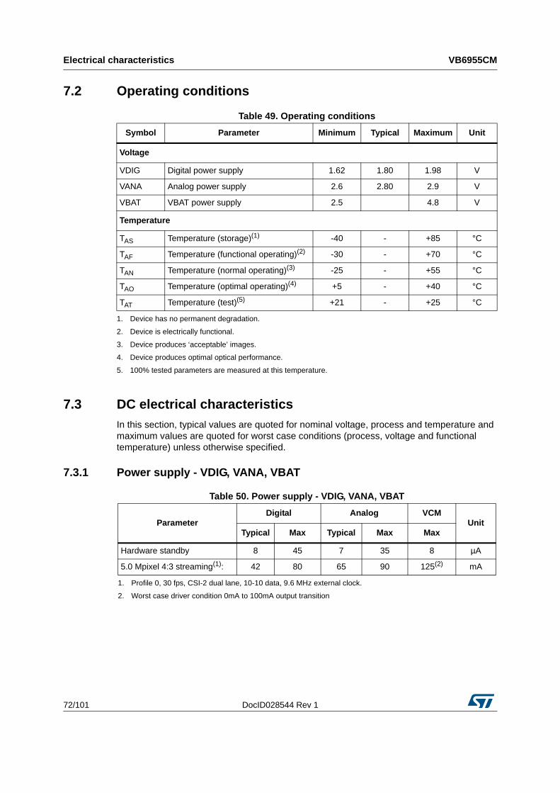
Electrical characteristics VB6955CM
72/101 DocID028544 Rev 1
7.2 Operating conditions
7.3 DC electrical characteristics
In this section, typical values are quoted for nominal voltage, process and temperature and maximum values are quoted for worst case conditions (process, voltage and functional temperature) unless otherwise specified.
7.3.1 Power supply - VDIG, VANA, VBAT
Table 49. Operating conditions
Symbol Parameter Minimum Typical Maximum Unit
Voltage
VDIG Digital power supply 1.62 1.80 1.98 V
VANA Analog power supply 2.6 2.80 2.9 V
VBAT VBAT power supply 2.5 4.8 V
Temperature
TAS Temperature (storage)(1)
1. Device has no permanent degradation.
-40 - +85 °C
TAF Temperature (functional operating)(2)
2. Device is electrically functional.
-30 - +70 °C
TAN Temperature (normal operating)(3)
3. Device produces ‘acceptable’ images.
-25 - +55 °C
TAO Temperature (optimal operating)(4)
4. Device produces optimal optical performance.
+5 - +40 °C
TAT Temperature (test)(5)
5. 100% tested parameters are measured at this temperature.
+21 - +25 °C
Table 50. Power supply - VDIG, VANA, VBAT
ParameterDigital Analog VCM
UnitTypical Max Typical Max Max
Hardware standby 8 45 7 35 8 µA
5.0 Mpixel 4:3 streaming(1):
1. Profile 0, 30 fps, CSI-2 dual lane, 10-10 data, 9.6 MHz external clock.
42 80 65 90 125(2)
2. Worst case driver condition 0mA to 100mA output transition
mA
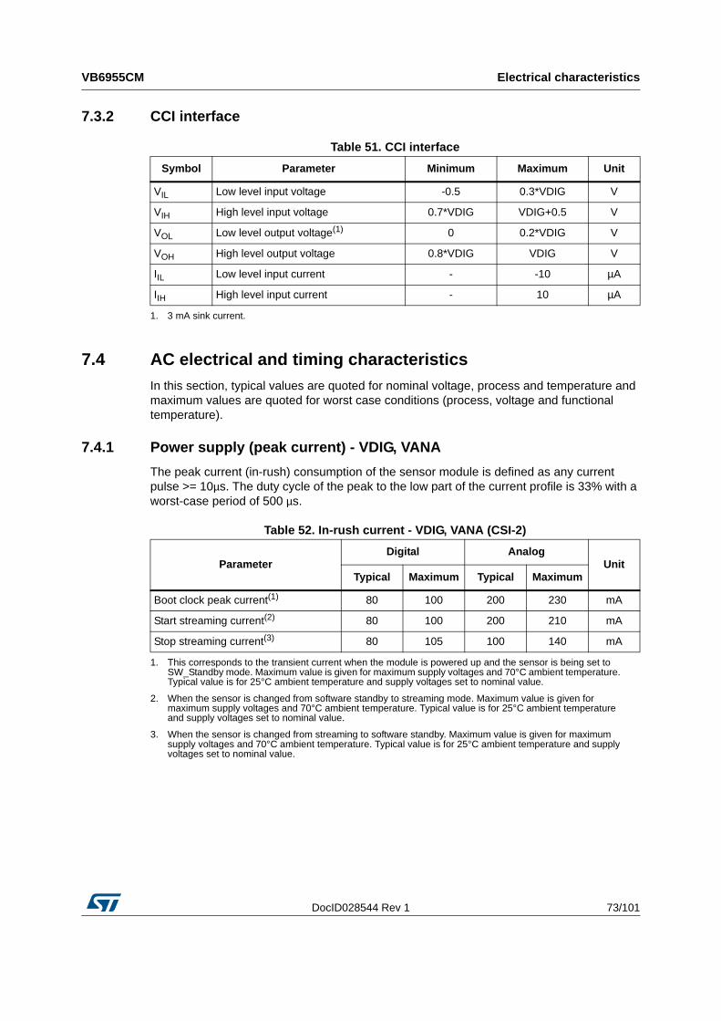
DocID028544 Rev 1 73/101
VB6955CM Electrical characteristics
76
7.3.2 CCI interface
7.4 AC electrical and timing characteristics
In this section, typical values are quoted for nominal voltage, process and temperature and maximum values are quoted for worst case conditions (process, voltage and functional temperature).
7.4.1 Power supply (peak current) - VDIG, VANA
The peak current (in-rush) consumption of the sensor module is defined as any current pulse >= 10µs. The duty cycle of the peak to the low part of the current profile is 33% with a worst-case period of 500 µs.
Table 51. CCI interface
Symbol Parameter Minimum Maximum Unit
VIL Low level input voltage -0.5 0.3*VDIG V
VIH High level input voltage 0.7*VDIG VDIG+0.5 V
VOL Low level output voltage(1)
1. 3 mA sink current.
0 0.2*VDIG V
VOH High level output voltage 0.8*VDIG VDIG V
IIL Low level input current - -10 µA
IIH High level input current - 10 µA
Table 52. In-rush current - VDIG, VANA (CSI-2)
ParameterDigital Analog
UnitTypical Maximum Typical Maximum
Boot clock peak current(1)
1. This corresponds to the transient current when the module is powered up and the sensor is being set to SW_Standby mode. Maximum value is given for maximum supply voltages and 70°C ambient temperature. Typical value is for 25°C ambient temperature and supply voltages set to nominal value.
80 100 200 230 mA
Start streaming current(2)
2. When the sensor is changed from software standby to streaming mode. Maximum value is given for maximum supply voltages and 70°C ambient temperature. Typical value is for 25°C ambient temperature and supply voltages set to nominal value.
80 100 200 210 mA
Stop streaming current(3)
3. When the sensor is changed from streaming to software standby. Maximum value is given for maximum supply voltages and 70°C ambient temperature. Typical value is for 25°C ambient temperature and supply voltages set to nominal value.
80 105 100 140 mA
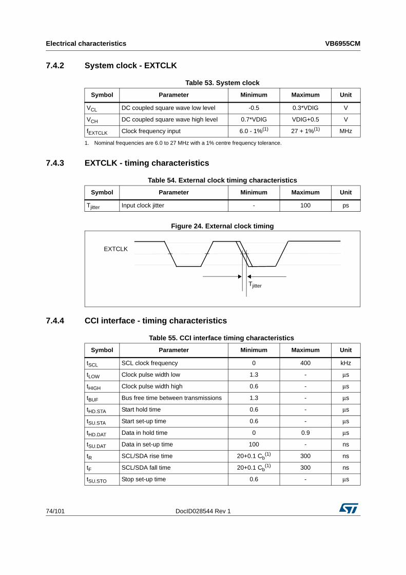
Electrical characteristics VB6955CM
74/101 DocID028544 Rev 1
7.4.2 System clock - EXTCLK
7.4.3 EXTCLK - timing characteristics
Figure 24. External clock timing
7.4.4 CCI interface - timing characteristics
Table 53. System clock
Symbol Parameter Minimum Maximum Unit
VCL DC coupled square wave low level -0.5 0.3*VDIG V
VCH DC coupled square wave high level 0.7*VDIG VDIG+0.5 V
fEXTCLK Clock frequency input 6.0 - 1%(1)
1. Nominal frequencies are 6.0 to 27 MHz with a 1% centre frequency tolerance.
27 + 1%(1) MHz
Table 54. External clock timing characteristics
Symbol Parameter Minimum Maximum Unit
Tjitter Input clock jitter - 100 ps
EXTCLK
Tjitter
Table 55. CCI interface timing characteristics
Symbol Parameter Minimum Maximum Unit
tSCL SCL clock frequency 0 400 kHz
tLOW Clock pulse width low 1.3 - μs
tHIGH Clock pulse width high 0.6 - μs
tBUF Bus free time between transmissions 1.3 - μs
tHD.STA Start hold time 0.6 - μs
tSU.STA Start set-up time 0.6 - μs
tHD.DAT Data in hold time 0 0.9 μs
tSU.DAT Data in set-up time 100 - ns
tR SCL/SDA rise time 20+0.1 Cb(1) 300 ns
tF SCL/SDA fall time 20+0.1 Cb(1) 300 ns
tSU.STO Stop set-up time 0.6 - μs
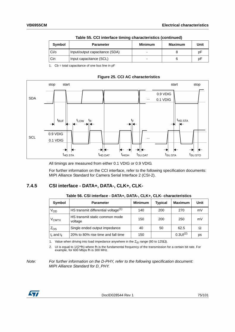
DocID028544 Rev 1 75/101
VB6955CM Electrical characteristics
76
Figure 25. CCI AC characteristics
All timings are measured from either 0.1 VDIG or 0.9 VDIG.
For further information on the CCI interface, refer to the following specification documents: MIPI Alliance Standard for Camera Serial Interface 2 (CSI-2).
7.4.5 CSI interface - DATA+, DATA-, CLK+, CLK-
Note: For further information on the D-PHY, refer to the following specification document: MIPI Alliance Standard for D_PHY.
Ci/o Input/output capacitance (SDA) - 8 pF
Cin Input capacitance (SCL) - 6 pF
1. Cb = total capacitance of one bus line in pF
Table 55. CCI interface timing characteristics (continued)
Symbol Parameter Minimum Maximum Unit
SDA
SCL
tHD.STA
tR
tHIGH
tF
tSU.DATtHD.DAT tSU.STA tSU.STO
...
...
tHD.STAtLOWtBUF
stopstartstop start
0.9 VDIG
0.1 VDIG
0.1 VDIG
0.9 VDIG
Table 56. CSI interface - DATA+, DATA-, CLK+, CLK- characteristics
Symbol Parameter Minimum Typical Maximum Unit
VOD HS transmit differential voltage(1)
1. Value when driving into load impedance anywhere in the ZID range (80 to 125Ω).
140 200 270 mV
VCMTXHS transmit static common mode voltage
150 200 250 mV
ZOS Single ended output impedance 40 50 62.5 Ω
tr and tf 20% to 80% rise time and fall time 150 0.3UI(2)
2. UI is equal to 1/(2*fh) where fh is the fundamental frequency of the transmission for a certain bit rate. For example, for 600 Mbps fh is 300 MHz.
ps
Optical specification VB6955CM
76/101 DocID028544 Rev 1
8 Optical specification
8.1 Lens characteristics
8.2 User precaution
As is common with many CMOS imagers, the camera should not be pointed at bright static objects for long periods of time as permanent damage to the sensor may occur.
Table 57. Lens design characteristics for first source lens supplier
Parameter Value
Construction 4-element plastic lens
F/number 2.4
Effective focal length 2.99 mm (primary wavelength 530 nm used)
Diagonal FOV 74° +/- 1°
Closest focusing distance 100 mm
DistortionTV: <|2%|
Absolute: <|1.0%| across whole field (by design)
Relative illumination (lens only) 40% at full image height, typical design value
Spectral weighting:
Wavlength (nm)
Weight
656.28
151
587.56
318
546.07
312
486.13
157
435.84
49
404.66
13
Lateral chromatic aberration from 435 nm to 656 nm
<2.8um
Coating reflectance - All surfaces are coated.
<1%
Maximum chief ray angle 29°
IR coating filter cut-off wavelength 650 nm +/-10 nm
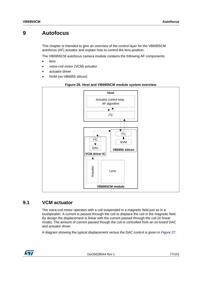
DocID028544 Rev 1 77/101
VB6955CM Autofocus
83
9 Autofocus
This chapter is intended to give an overview of the control layer for the VB6955CM autofocus (AF) actuator and explain how to control the lens position.
The VB6955CM autofocus camera module contains the following AF components:
• lens
• voice-coil motor (VCM) actuator
• actuator driver
• NVM (on VB6955 silicon)
Figure 26. Host and VB6955CM module system overview
9.1 VCM actuator
The voice-coil motor operates with a coil suspended in a magnetic field just as in a loudspeaker. A current is passed through the coil to displace the coil in the magnetic field. By design the displacement is linear with the current passed through the coil (in linear mode). The amount of current passed though the coil is controlled from an on-board DAC and actuator driver.
A diagram showing the typical displacement versus the DAC control is given in Figure 27.
Host
VB6955CM module
I2C
Lens
Act
uato
r
I2C
Actuator control loop,
DAC
NVM
VB6955 silicon
AF algorithm
I2C
VCM driver IC
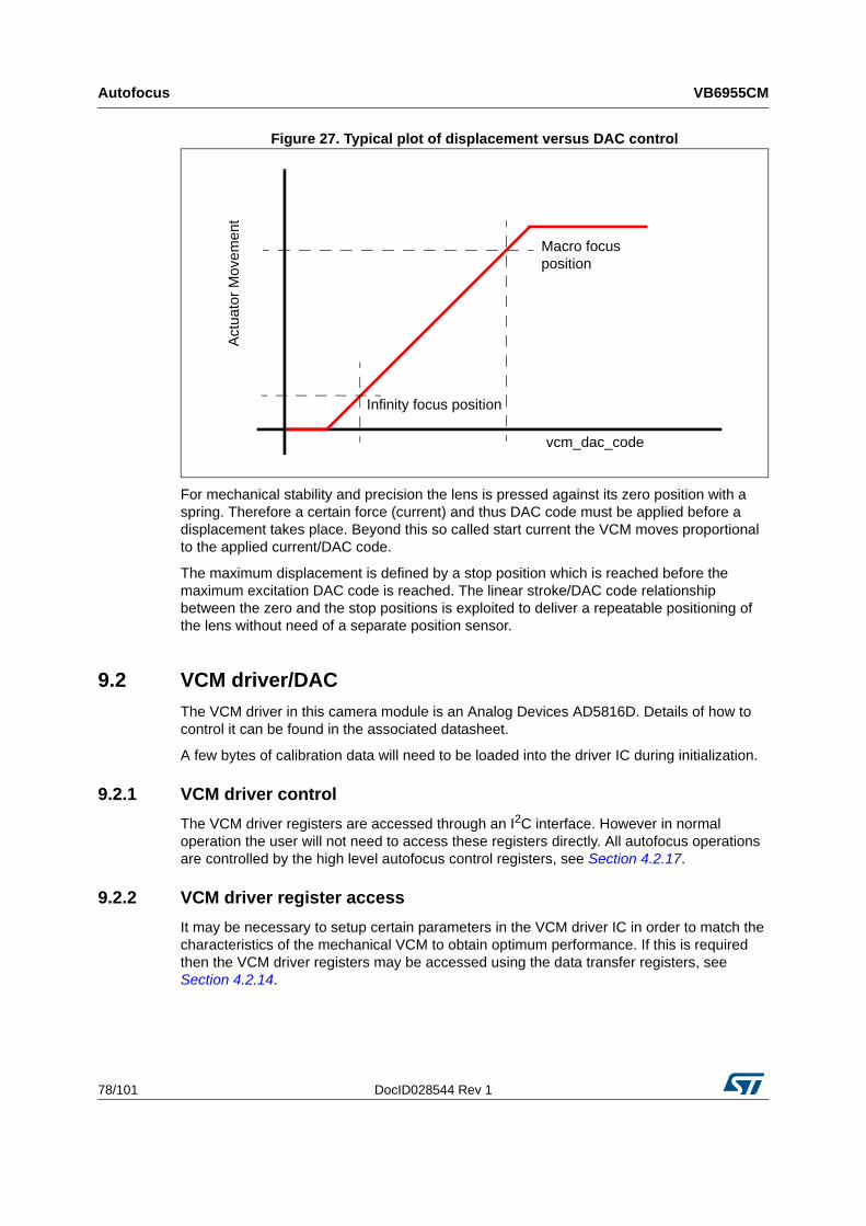
Autofocus VB6955CM
78/101 DocID028544 Rev 1
Figure 27. Typical plot of displacement versus DAC control
For mechanical stability and precision the lens is pressed against its zero position with a spring. Therefore a certain force (current) and thus DAC code must be applied before a displacement takes place. Beyond this so called start current the VCM moves proportional to the applied current/DAC code.
The maximum displacement is defined by a stop position which is reached before the maximum excitation DAC code is reached. The linear stroke/DAC code relationship between the zero and the stop positions is exploited to deliver a repeatable positioning of the lens without need of a separate position sensor.
9.2 VCM driver/DAC
The VCM driver in this camera module is an Analog Devices AD5816D. Details of how to control it can be found in the associated datasheet.
A few bytes of calibration data will need to be loaded into the driver IC during initialization.
9.2.1 VCM driver control
The VCM driver registers are accessed through an I2C interface. However in normal operation the user will not need to access these registers directly. All autofocus operations are controlled by the high level autofocus control registers, see Section 4.2.17.
9.2.2 VCM driver register access
It may be necessary to setup certain parameters in the VCM driver IC in order to match the characteristics of the mechanical VCM to obtain optimum performance. If this is required then the VCM driver registers may be accessed using the data transfer registers, see Section 4.2.14.
vcm_dac_code
Act
ua
tor
Mo
vem
en
tMacro focus position
Infinity focus position
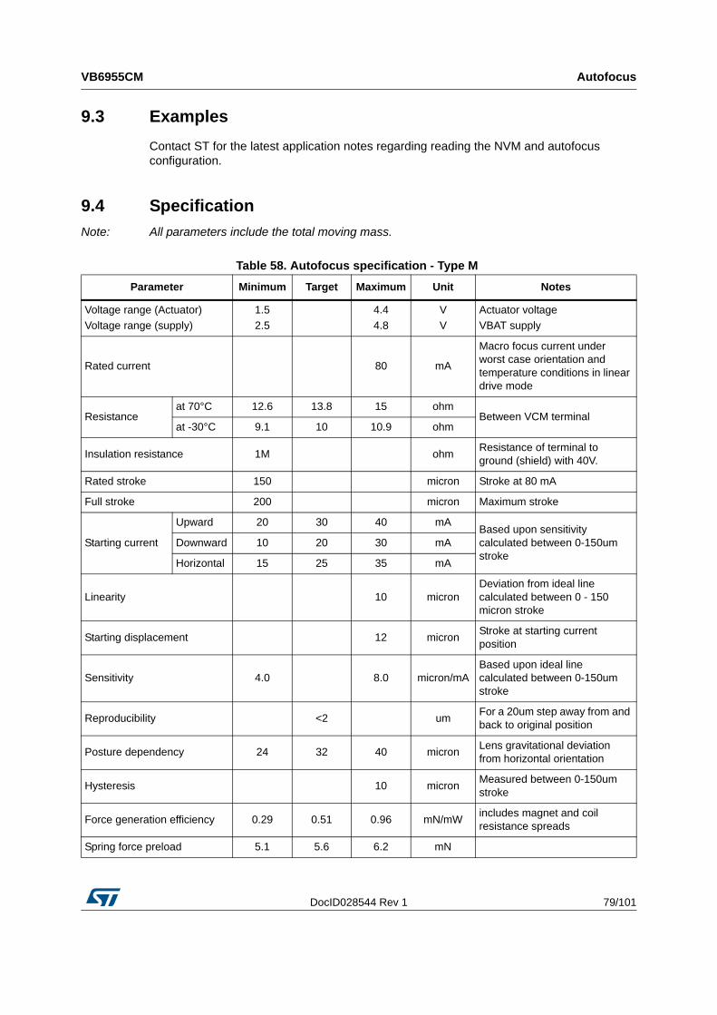
DocID028544 Rev 1 79/101
VB6955CM Autofocus
83
9.3 Examples
Contact ST for the latest application notes regarding reading the NVM and autofocus configuration.
9.4 Specification
Note: All parameters include the total moving mass.
Table 58. Autofocus specification - Type M
Parameter Minimum Target Maximum Unit Notes
Voltage range (Actuator)
Voltage range (supply)
1.5
2.5
4.4
4.8
V
V
Actuator voltage
VBAT supply
Rated current 80 mA
Macro focus current under worst case orientation and temperature conditions in linear drive mode
Resistance at 70°C 12.6 13.8 15 ohm
Between VCM terminalat -30°C 9.1 10 10.9 ohm
Insulation resistance 1M ohmResistance of terminal to ground (shield) with 40V.
Rated stroke 150 micron Stroke at 80 mA
Full stroke 200 micron Maximum stroke
Starting current
Upward 20 30 40 mABased upon sensitivity calculated between 0-150um stroke
Downward 10 20 30 mA
Horizontal 15 25 35 mA
Linearity 10 micronDeviation from ideal line calculated between 0 - 150 micron stroke
Starting displacement 12 micronStroke at starting current position
Sensitivity 4.0 8.0 micron/mABased upon ideal line calculated between 0-150um stroke
Reproducibility <2 umFor a 20um step away from and back to original position
Posture dependency 24 32 40 micronLens gravitational deviation from horizontal orientation
Hysteresis 10 micronMeasured between 0-150um stroke
Force generation efficiency 0.29 0.51 0.96 mN/mWincludes magnet and coil resistance spreads
Spring force preload 5.1 5.6 6.2 mN
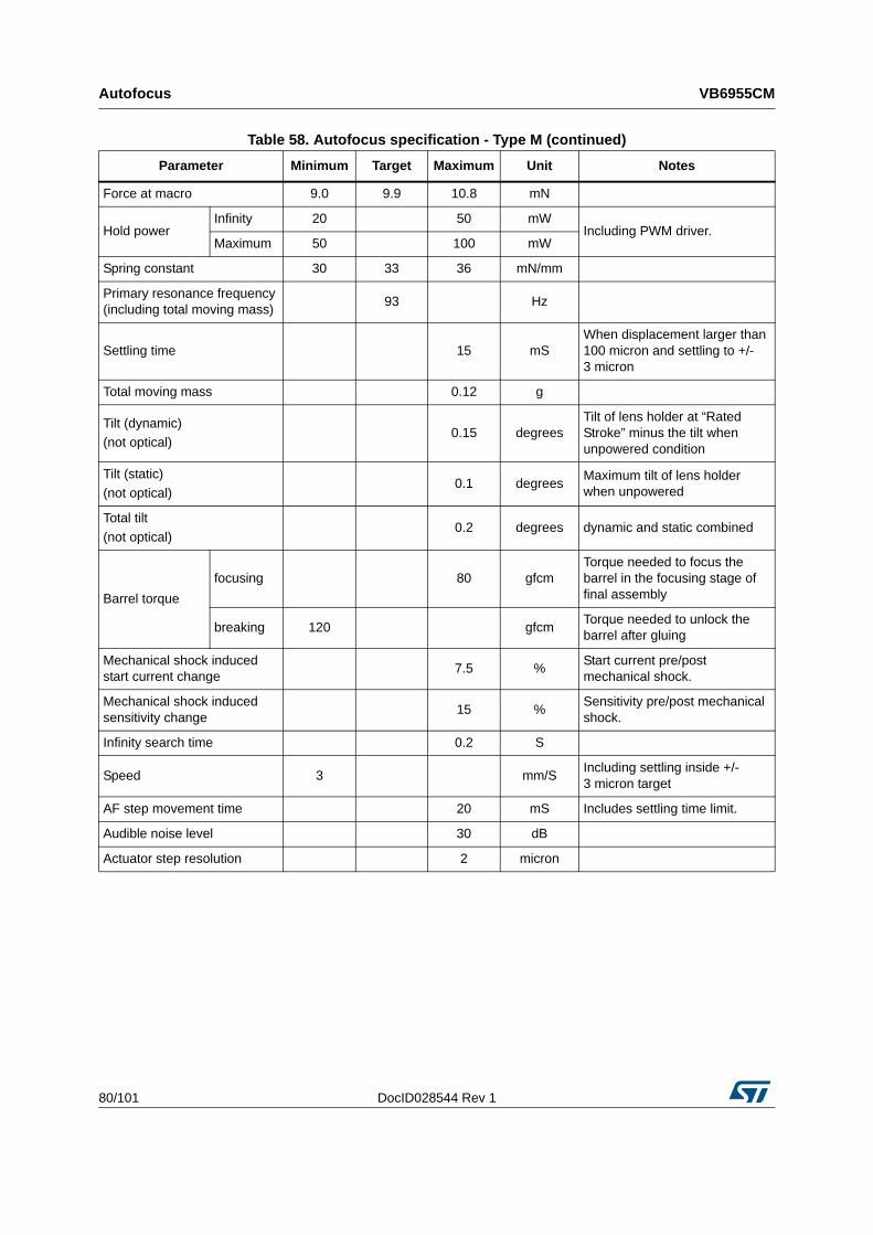
Autofocus VB6955CM
80/101 DocID028544 Rev 1
Force at macro 9.0 9.9 10.8 mN
Hold powerInfinity 20 50 mW
Including PWM driver. Maximum 50 100 mW
Spring constant 30 33 36 mN/mm
Primary resonance frequency (including total moving mass)
93 Hz
Settling time 15 mSWhen displacement larger than 100 micron and settling to +/-3 micron
Total moving mass 0.12 g
Tilt (dynamic)
(not optical)0.15 degrees
Tilt of lens holder at “Rated Stroke” minus the tilt when unpowered condition
Tilt (static)
(not optical)0.1 degrees
Maximum tilt of lens holder when unpowered
Total tilt
(not optical)0.2 degrees dynamic and static combined
Barrel torque
focusing 80 gfcmTorque needed to focus the barrel in the focusing stage of final assembly
breaking 120 gfcmTorque needed to unlock the barrel after gluing
Mechanical shock induced start current change
7.5 %Start current pre/post mechanical shock.
Mechanical shock induced sensitivity change
15 %Sensitivity pre/post mechanical shock.
Infinity search time 0.2 S
Speed 3 mm/SIncluding settling inside +/-3 micron target
AF step movement time 20 mS Includes settling time limit.
Audible noise level 30 dB
Actuator step resolution 2 micron
Table 58. Autofocus specification - Type M (continued)
Parameter Minimum Target Maximum Unit Notes
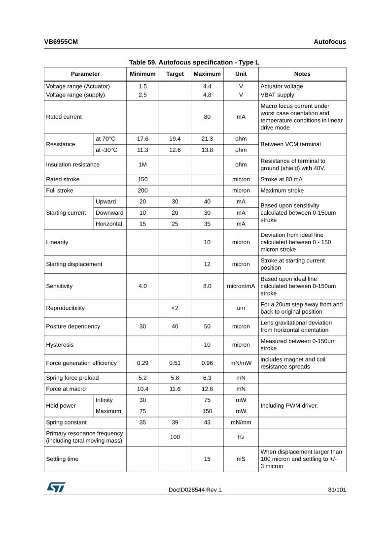
DocID028544 Rev 1 81/101
VB6955CM Autofocus
83
Table 59. Autofocus specification - Type L
Parameter Minimum Target Maximum Unit Notes
Voltage range (Actuator)
Voltage range (supply)
1.5
2.5
4.4
4.8
V
V
Actuator voltage
VBAT supply
Rated current 80 mA
Macro focus current under worst case orientation and temperature conditions in linear drive mode
Resistance at 70°C 17.6 19.4 21.3 ohm
Between VCM terminalat -30°C 11.3 12.6 13.8 ohm
Insulation resistance 1M ohmResistance of terminal to ground (shield) with 40V.
Rated stroke 150 micron Stroke at 80 mA
Full stroke 200 micron Maximum stroke
Starting current
Upward 20 30 40 mABased upon sensitivity calculated between 0-150um stroke
Downward 10 20 30 mA
Horizontal 15 25 35 mA
Linearity 10 micronDeviation from ideal line calculated between 0 - 150 micron stroke
Starting displacement 12 micronStroke at starting current position
Sensitivity 4.0 8.0 micron/mABased upon ideal line calculated between 0-150um stroke
Reproducibility <2 umFor a 20um step away from and back to original position
Posture dependency 30 40 50 micronLens gravitational deviation from horizontal orientation
Hysteresis 10 micronMeasured between 0-150um stroke
Force generation efficiency 0.29 0.51 0.96 mN/mWincludes magnet and coil resistance spreads
Spring force preload 5.2 5.8 6.3 mN
Force at macro 10.4 11.6 12.6 mN
Hold powerInfinity 30 75 mW
Including PWM driver. Maximum 75 150 mW
Spring constant 35 39 43 mN/mm
Primary resonance frequency (including total moving mass)
100 Hz
Settling time 15 mSWhen displacement larger than 100 micron and settling to +/-3 micron
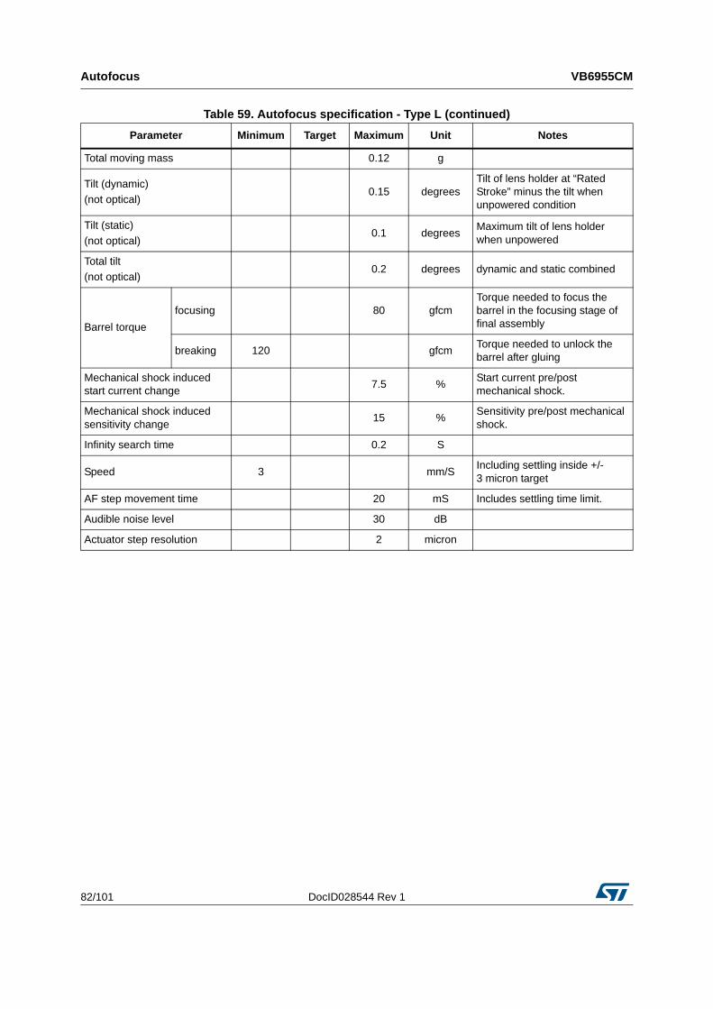
Autofocus VB6955CM
82/101 DocID028544 Rev 1
Total moving mass 0.12 g
Tilt (dynamic)
(not optical)0.15 degrees
Tilt of lens holder at “Rated Stroke” minus the tilt when unpowered condition
Tilt (static)
(not optical)0.1 degrees
Maximum tilt of lens holder when unpowered
Total tilt
(not optical)0.2 degrees dynamic and static combined
Barrel torque
focusing 80 gfcmTorque needed to focus the barrel in the focusing stage of final assembly
breaking 120 gfcmTorque needed to unlock the barrel after gluing
Mechanical shock induced start current change
7.5 %Start current pre/post mechanical shock.
Mechanical shock induced sensitivity change
15 %Sensitivity pre/post mechanical shock.
Infinity search time 0.2 S
Speed 3 mm/SIncluding settling inside +/-3 micron target
AF step movement time 20 mS Includes settling time limit.
Audible noise level 30 dB
Actuator step resolution 2 micron
Table 59. Autofocus specification - Type L (continued)
Parameter Minimum Target Maximum Unit Notes
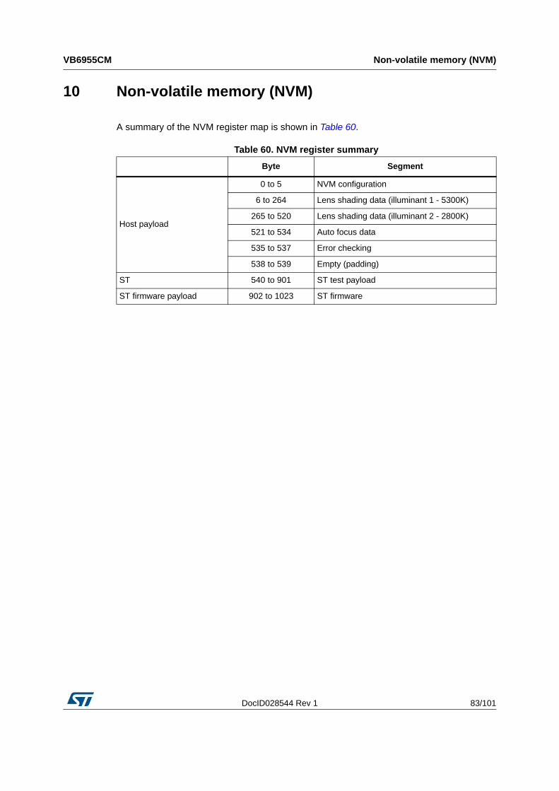
DocID028544 Rev 1 83/101
VB6955CM Non-volatile memory (NVM)
83
10 Non-volatile memory (NVM)
A summary of the NVM register map is shown in Table 60.
Table 60. NVM register summary
Byte Segment
Host payload
0 to 5 NVM configuration
6 to 264 Lens shading data (illuminant 1 - 5300K)
265 to 520 Lens shading data (illuminant 2 - 2800K)
521 to 534 Auto focus data
535 to 537 Error checking
538 to 539 Empty (padding)
ST 540 to 901 ST test payload
ST firmware payload 902 to 1023 ST firmware
Defect categorization VB6955CM
84/101 DocID028544 Rev 1
11 Defect categorization
11.1 Pixel defects
11.1.1 Overview
Pixel defect density measures the average number of defective pixels per color channel under “Diffuse” and “Dark” conditions, refer to Table 61.
11.1.2 Defect detection
Defect detection is performed in two parts; once in diffuse conditions and once in dark conditions, as defined in Table 61. The methods used for these differ to account for the differing conditions and for the difference in the failure modes detected by each.
In both the dark and light cases, two images are averaged pixel-by-pixel in order to reduce the impact of temporal noise. Detection is performed individually on the four colour channels.
“Dark defects” are those which appear too bright in a dark image, either due to dark current or a stuck-at fault. These are measured by thresholding against the difference between the actual pixel value and the local or full-frame average (this is dependent on the uniformity of the dark image). The threshold is defined such that it can identify gain error above the normal noise distribution of photon shot noise and sensor noise and so pixels that deviate by more than the dark threshold are declared defective.
“Light defects” tend to be caused by small foreign material or damage to the die surface. The diffused image is processed to remove very low frequency variation by gaining the image towards the centre peak value for each colour channel, mimicking the lens shading gains applied in the application. Pixels that deviate from the local average by more than the light threshold in either direction are defined as defective. The 64-code pedestal is not removed from this relative calculation.
Table 61. Pixel defect specification
Reference Area Threshold
Dark Full Channel 64 codes
Light 9x9 +/-12%
Table 62. Image settings
Dark Diffuse
Exposure 100ms 33ms(1)
1. Image exposure targets 75% of full-scale deflection in the green channels at the centre of the image.
Analog gain x8 x1
Digital gain x1 x1
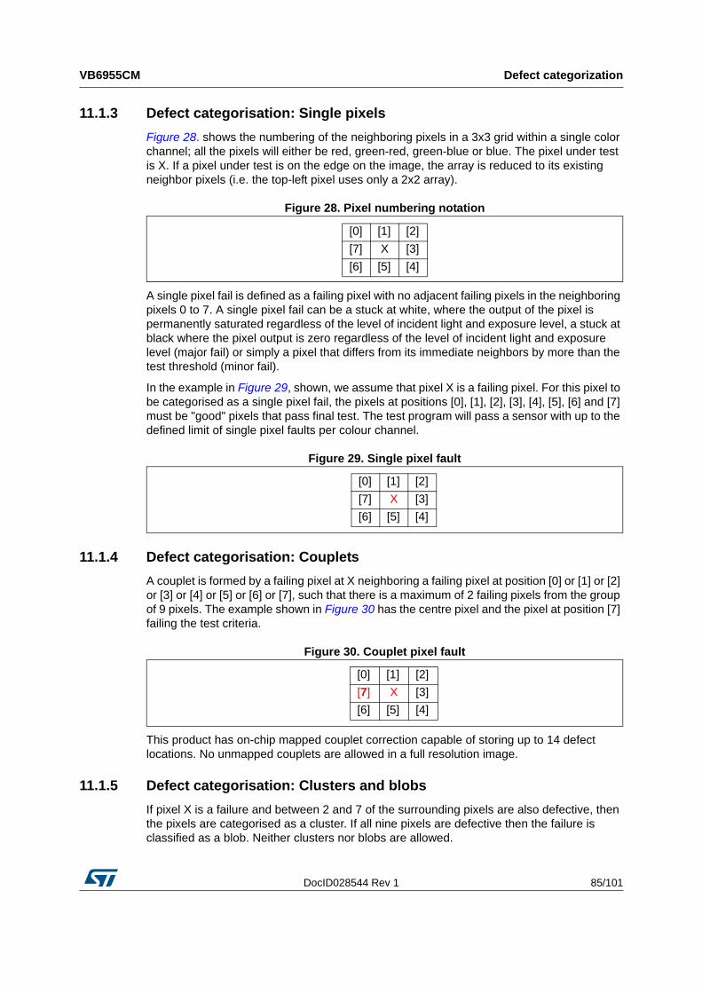
DocID028544 Rev 1 85/101
VB6955CM Defect categorization
96
11.1.3 Defect categorisation: Single pixels
Figure 28. shows the numbering of the neighboring pixels in a 3x3 grid within a single color channel; all the pixels will either be red, green-red, green-blue or blue. The pixel under test is X. If a pixel under test is on the edge on the image, the array is reduced to its existing neighbor pixels (i.e. the top-left pixel uses only a 2x2 array).
Figure 28. Pixel numbering notation
A single pixel fail is defined as a failing pixel with no adjacent failing pixels in the neighboring pixels 0 to 7. A single pixel fail can be a stuck at white, where the output of the pixel is permanently saturated regardless of the level of incident light and exposure level, a stuck at black where the pixel output is zero regardless of the level of incident light and exposure level (major fail) or simply a pixel that differs from its immediate neighbors by more than the test threshold (minor fail).
In the example in Figure 29, shown, we assume that pixel X is a failing pixel. For this pixel to be categorised as a single pixel fail, the pixels at positions [0], [1], [2], [3], [4], [5], [6] and [7] must be "good" pixels that pass final test. The test program will pass a sensor with up to the defined limit of single pixel faults per colour channel.
Figure 29. Single pixel fault
11.1.4 Defect categorisation: Couplets
A couplet is formed by a failing pixel at X neighboring a failing pixel at position [0] or [1] or [2] or [3] or [4] or [5] or [6] or [7], such that there is a maximum of 2 failing pixels from the group of 9 pixels. The example shown in Figure 30 has the centre pixel and the pixel at position [7] failing the test criteria.
Figure 30. Couplet pixel fault
This product has on-chip mapped couplet correction capable of storing up to 14 defect locations. No unmapped couplets are allowed in a full resolution image.
11.1.5 Defect categorisation: Clusters and blobs
If pixel X is a failure and between 2 and 7 of the surrounding pixels are also defective, then the pixels are categorised as a cluster. If all nine pixels are defective then the failure is classified as a blob. Neither clusters nor blobs are allowed.
[0] [1] [2]
[7] X [3]
[6] [5] [4]
[0] [1] [2]
[7] X [3]
[6] [5] [4]
[0] [1] [2]
[7] X [3]
[6] [5] [4]
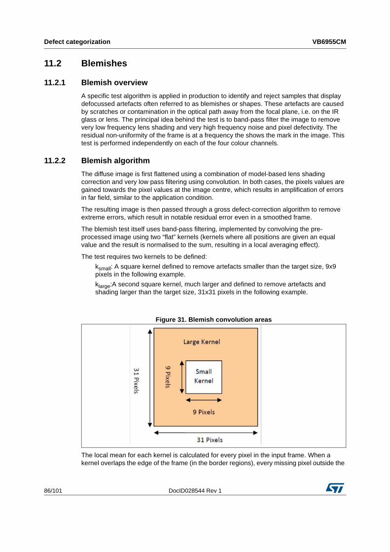
Defect categorization VB6955CM
86/101 DocID028544 Rev 1
11.2 Blemishes
11.2.1 Blemish overview
A specific test algorithm is applied in production to identify and reject samples that display defocussed artefacts often referred to as blemishes or shapes. These artefacts are caused by scratches or contamination in the optical path away from the focal plane, i.e. on the IR glass or lens. The principal idea behind the test is to band-pass filter the image to remove very low frequency lens shading and very high frequency noise and pixel defectivity. The residual non-uniformity of the frame is at a frequency the shows the mark in the image. This test is performed independently on each of the four colour channels.
11.2.2 Blemish algorithm
The diffuse image is first flattened using a combination of model-based lens shading correction and very low pass filtering using convolution. In both cases, the pixels values are gained towards the pixel values at the image centre, which results in amplification of errors in far field, similar to the application condition.
The resulting image is then passed through a gross defect-correction algorithm to remove extreme errors, which result in notable residual error even in a smoothed frame.
The blemish test itself uses band-pass filtering, implemented by convolving the pre-processed image using two “flat” kernels (kernels where all positions are given an equal value and the result is normalised to the sum, resulting in a local averaging effect).
The test requires two kernels to be defined:
ksmall: A square kernel defined to remove artefacts smaller than the target size, 9x9 pixels in the following example.
klarge:A second square kernel, much larger and defined to remove artefacts and shading larger than the target size, 31x31 pixels in the following example.
Figure 31. Blemish convolution areas
The local mean for each kernel is calculated for every pixel in the input frame. When a kernel overlaps the edge of the frame (in the border regions), every missing pixel outside the
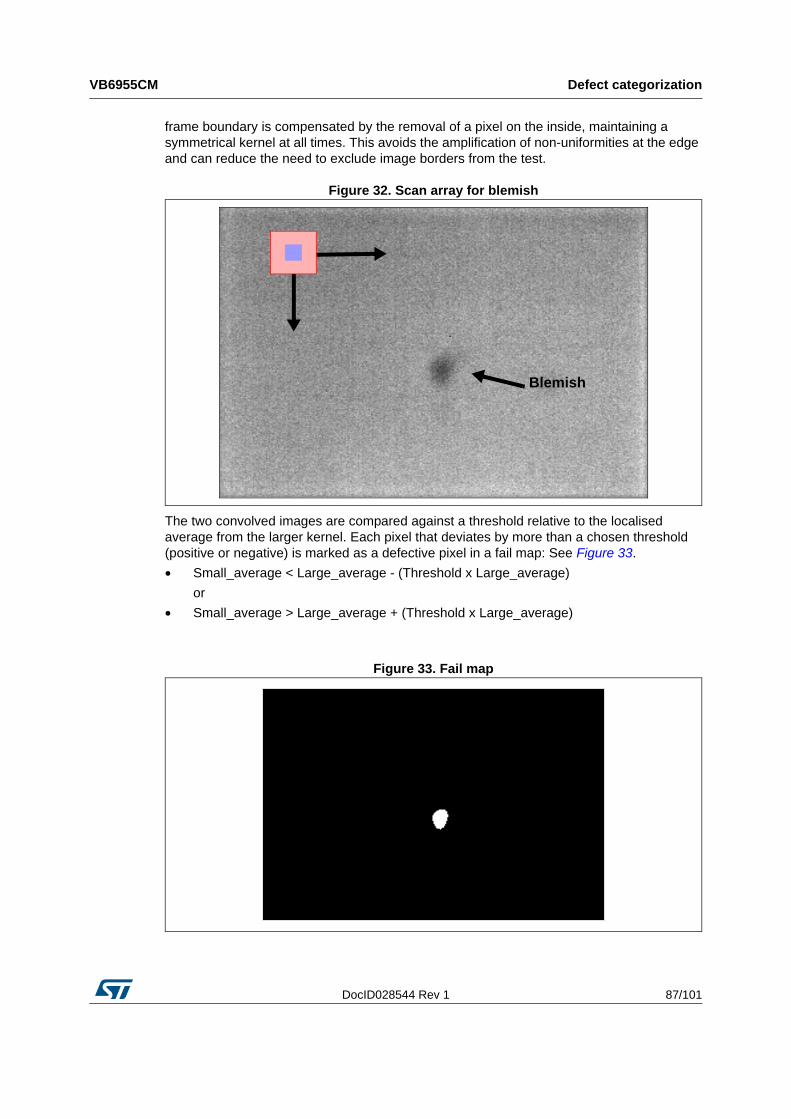
DocID028544 Rev 1 87/101
VB6955CM Defect categorization
96
frame boundary is compensated by the removal of a pixel on the inside, maintaining a symmetrical kernel at all times. This avoids the amplification of non-uniformities at the edge and can reduce the need to exclude image borders from the test.
Figure 32. Scan array for blemish
The two convolved images are compared against a threshold relative to the localised average from the larger kernel. Each pixel that deviates by more than a chosen threshold (positive or negative) is marked as a defective pixel in a fail map: See Figure 33.
• Small_average < Large_average - (Threshold x Large_average)
or
• Small_average > Large_average + (Threshold x Large_average)
Figure 33. Fail map
Blemish
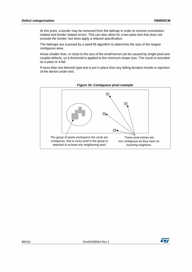
Defect categorization VB6955CM
88/101 DocID028544 Rev 1
At this point, a border may be removed from the failmap in order to remove convolution related and border related errors. This can also allow for a two pass test that does not exclude the border, but does apply a relaxed specification.
The failmaps are scanned by a seed-fill algorithm to determine the size of the largest contiguous area.
Areas smaller than, or close to the size of the small kernel can be caused by single pixel and couplet defects, so a threshold is applied to the minimum shape size. The result is recorded as a pass or a fail.
If more than one blemish type test is put in place then any failing iteration results in rejection of the device under test.
Figure 34. Contiguous pixel example
The group of pixels enclosed in the circle are contiguous, that is every pixel in the group is
attached to at least one neighboring pixel.
These pixel entries arenon contiguous as they have no
touching neighbors.
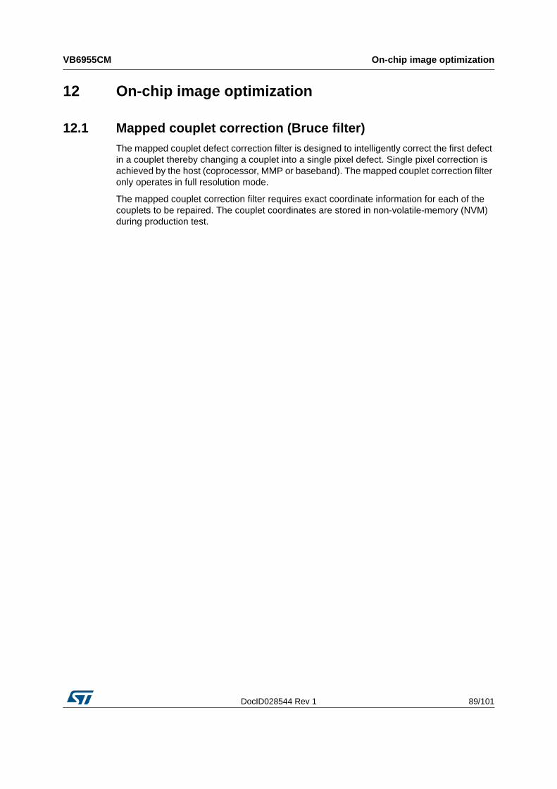
DocID028544 Rev 1 89/101
VB6955CM On-chip image optimization
96
12 On-chip image optimization
12.1 Mapped couplet correction (Bruce filter)
The mapped couplet defect correction filter is designed to intelligently correct the first defect in a couplet thereby changing a couplet into a single pixel defect. Single pixel correction is achieved by the host (coprocessor, MMP or baseband). The mapped couplet correction filter only operates in full resolution mode.
The mapped couplet correction filter requires exact coordinate information for each of the couplets to be repaired. The couplet coordinates are stored in non-volatile-memory (NVM) during production test.
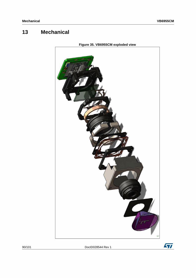
Mechanical VB6955CM
90/101 DocID028544 Rev 1
13 Mechanical
Figure 35. VB6955CM exploded view
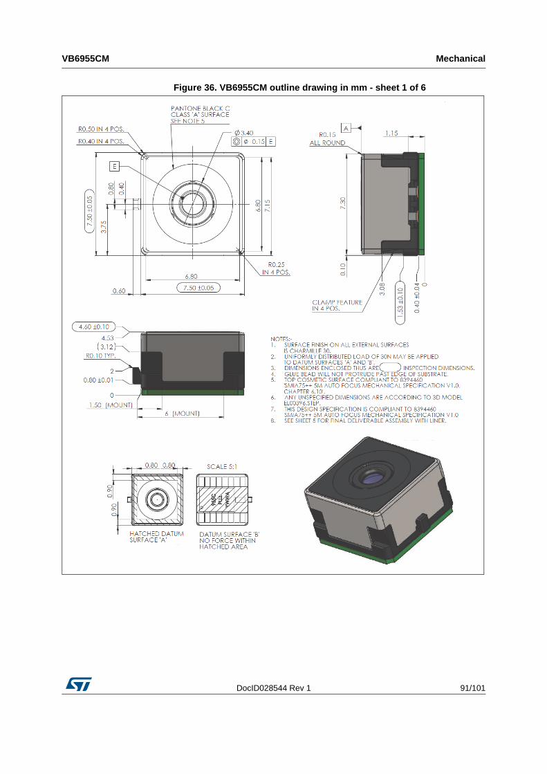
DocID028544 Rev 1 91/101
VB6955CM Mechanical
96
Figure 36. VB6955CM outline drawing in mm - sheet 1 of 6
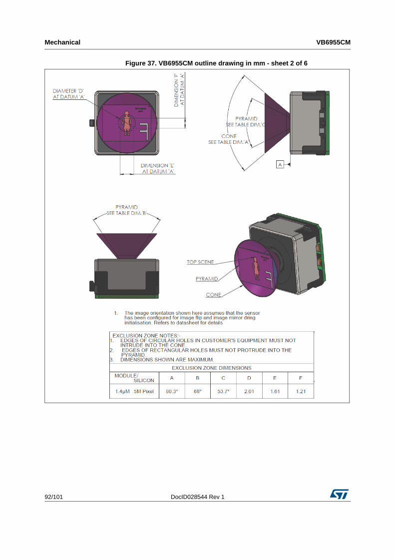
Mechanical VB6955CM
92/101 DocID028544 Rev 1
Figure 37. VB6955CM outline drawing in mm - sheet 2 of 6
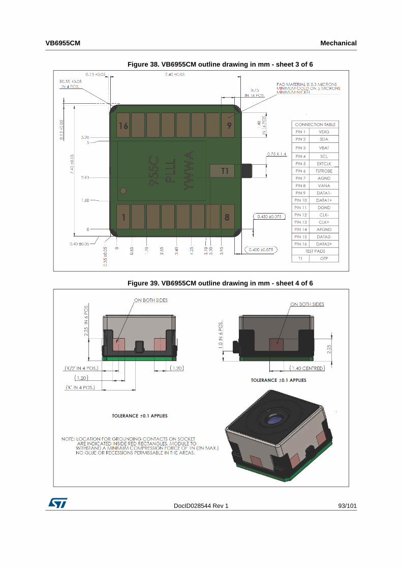
DocID028544 Rev 1 93/101
VB6955CM Mechanical
96
Figure 38. VB6955CM outline drawing in mm - sheet 3 of 6
Figure 39. VB6955CM outline drawing in mm - sheet 4 of 6
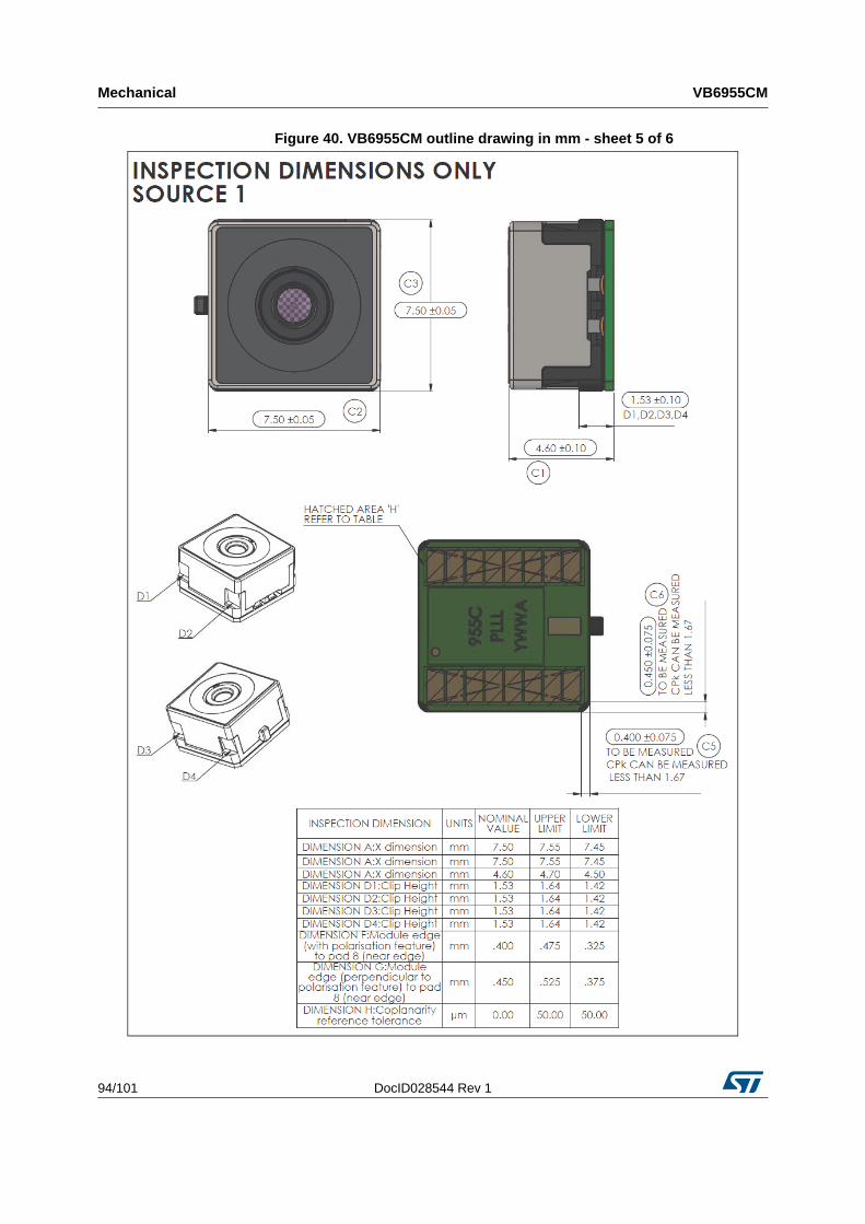
Mechanical VB6955CM
94/101 DocID028544 Rev 1
Figure 40. VB6955CM outline drawing in mm - sheet 5 of 6
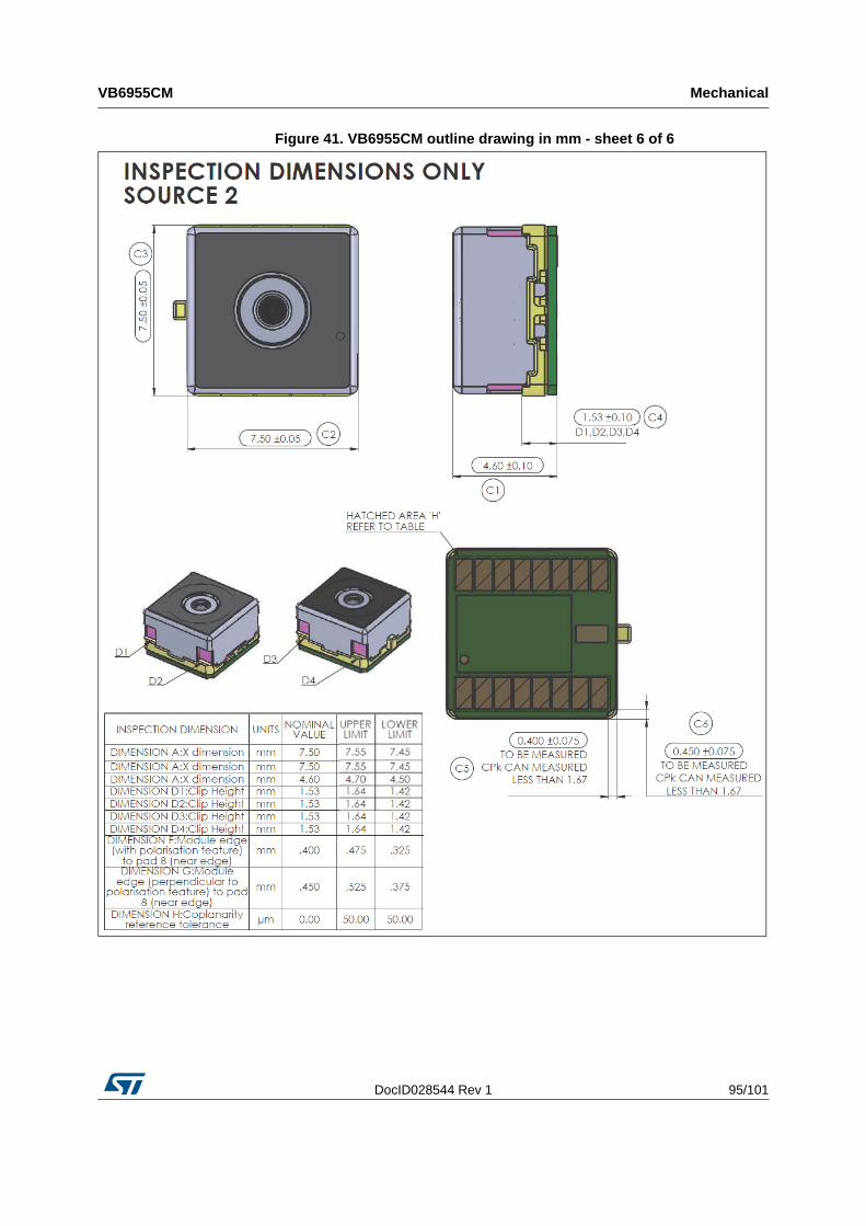
DocID028544 Rev 1 95/101
VB6955CM Mechanical
96
Figure 41. VB6955CM outline drawing in mm - sheet 6 of 6
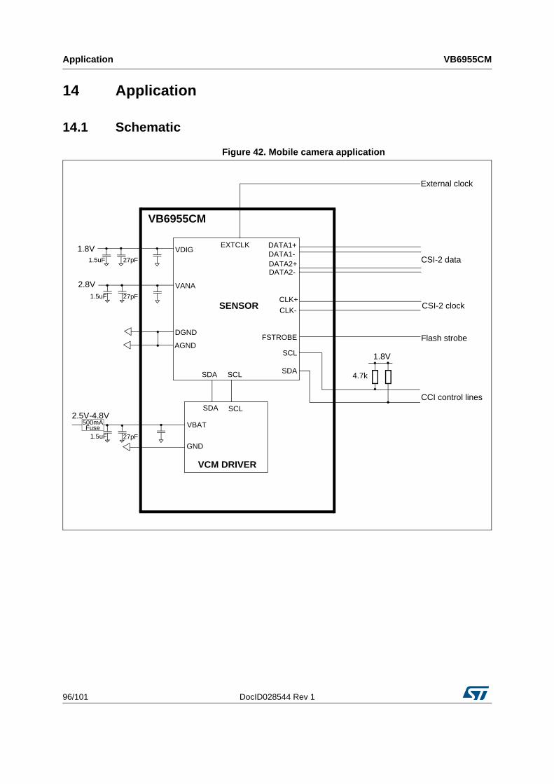
Application VB6955CM
96/101 DocID028544 Rev 1
14 Application
14.1 Schematic
Figure 42. Mobile camera application
VB6955CM
1.8V EXTCLK DATA1+
CLK-
DGND
AGNDSCL
SDA
1.8V
External clock
Flash strobe
4.7k
FSTROBE
DATA1-
CLK+
CSI-2 data
CSI-2 clock
CCI control lines
VDIG
2.8V VANA
SENSOR
VCM DRIVER
SDA SCL
GND
VBAT2.5V-4.8V
DATA2-DATA2+
SCLSDA
1.5uF 27pF
1.5uF 27pF
1.5uF 27pF
500mAFuse
DocID028544 Rev 1 97/101
VB6955CM Acronyms and abbreviations
98
15 Acronyms and abbreviations
Table 63. Acronyms and abbreviations
Acronym/abbreviation
Definition
CCI Camera control interface
CMI Camera module integrator
CSI Camera serial interface
DPCM Differential pulse code modulation
EMC Electromagnetic compatibility
EMI Electromagnetic interference
EOF End of frame
EOT End of transmission
FE Frame end
fps Frames per second
FS Frame start
HS High speed; identifier for operation mode
HS-RX High speed receiver (low-swing differential)
HS-TX High speed transmitter (low-swing differential)
I2C Inter ICbus
LE Line end
LLP Low level protocol
LS Line start
LSB Least significant byte
LP Low power; identifier for operation mode
LP-RX Low power receiver (large-swing single ended)
LP-TX Low power transmitter (large-swing single ended)
LVDS Low voltage differential signaling
Mbps Megabits per second
MIPI Mobile industry processor interface
MSB Most significant byte
PCK Pixel clock
PCM Pulse code modulation
PF Packet footer
PH Packet header
PI Packet identifier
PT Packet type
Acronyms and abbreviations VB6955CM
98/101 DocID028544 Rev 1
PHY Physical layer
PLL Phase locked loop
RO Read only
RW Read/write
SCL Serial clock (for CCI)
SDA Serial data (for CCI)
SMIA Standard mobile imaging architecture
SOT Start of transmission
SOF Start of frame
SSCG Spread spectrum clock generator
SubLVDS Sub-low voltage differential signaling
WDR Wide dynamic reconstructor
ULPM Ultra low power mode
Table 63. Acronyms and abbreviations (continued)
Acronym/abbreviation
Definition
DocID028544 Rev 1 99/101
VB6955CM ECOPACK®
100
16 ECOPACK®
In order to meet environmental requirements, ST offers these devices in different grades of ECOPACK® packages, depending on their level of environmental compliance. ECOPACK® specifications, grade definitions and product status are available at: www.st.com. ECOPACK® is an ST trademark.
Revision history VB6955CM
100/101 DocID028544 Rev 1
17 Revision history
Table 64. Document revision history
Date Revision Changes
22-Oct-2015 1 Initial release
DocID028544 Rev 1 101/101
VB6955CM
101
IMPORTANT NOTICE – PLEASE READ CAREFULLY
STMicroelectronics NV and its subsidiaries (“ST”) reserve the right to make changes, corrections, enhancements, modifications, and improvements to ST products and/or to this document at any time without notice. Purchasers should obtain the latest relevant information on ST products before placing orders. ST products are sold pursuant to ST’s terms and conditions of sale in place at the time of order acknowledgement.
Purchasers are solely responsible for the choice, selection, and use of ST products and ST assumes no liability for application assistance or the design of Purchasers’ products.
No license, express or implied, to any intellectual property right is granted by ST herein.
Resale of ST products with provisions different from the information set forth herein shall void any warranty granted by ST for such product.
ST and the ST logo are trademarks of ST. All other product or service names are the property of their respective owners.
Information in this document supersedes and replaces information previously supplied in any prior versions of this document.
© 2015 STMicroelectronics – All rights reserved