Embed Size (px)
Citation preview
5 kV rms Signal Isolated High Speed CAN Transceiver with Bus Protection
Data Sheet ADM3054
Rev. D Document Feedback Information furnished by Analog Devices is believed to be accurate and reliable. However, no responsibility is assumed by Analog Devices for its use, nor for any infringements of patents or other rights of third parties that may result from its use. Specifications subject to change without notice. No license is granted by implication or otherwise under any patent or patent rights of Analog Devices. Trademarks and registered trademarks are the property of their respective owners.
One Technology Way, P.O. Box 9106, Norwood, MA 02062-9106, U.S.A.Tel: 781.329.4700 ©2011–2017 Analog Devices, Inc. All rights reserved. Technical Support www.analog.com
FEATURES 5 kV rms signal isolated CAN transceiver 5 V or 3.3 V operation on VDD1 5 V operation on VDD2 VDD2SENSE to detect loss of power on VDD2 Complies with ISO 11898 standard High speed data rates of up to 1 Mbps Short-circuit protection on CANH and CANL against shorts to
power/ground in 24 V systems Unpowered nodes do not disturb the bus Connect 110 or more nodes on the bus Thermal shutdown protection High common-mode transient immunity: >25 kV/μs Safety and regulatory approvals
UL recognition 5000 V rms for 1 minute per UL 1577
VDE Certificates of Conformity DIN V VDE V 0884-10 (VDE V 0884-10): 2006-12 VIORM = 846 V peak
Industrial operating temperature range: −40°C to +125°C Wide-body, 16-lead SOIC package Qualified for automotive applications
APPLICATIONS CAN data buses Industrial field networks
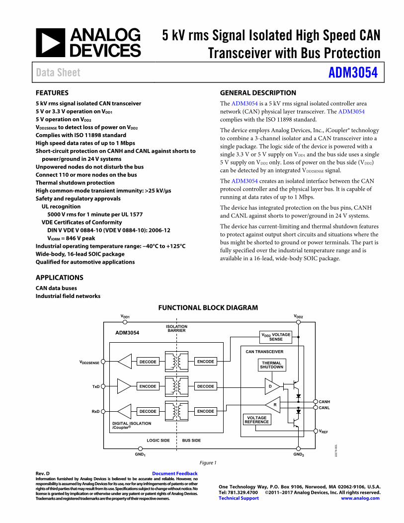
GENERAL DESCRIPTION The ADM3054 is a 5 kV rms signal isolated controller area network (CAN) physical layer transceiver. The ADM3054 complies with the ISO 11898 standard.
The device employs Analog Devices, Inc., iCoupler® technology to combine a 3-channel isolator and a CAN transceiver into a single package. The logic side of the device is powered with a single 3.3 V or 5 V supply on VDD1 and the bus side uses a single 5 V supply on VDD2 only. Loss of power on the bus side (VDD2) can be detected by an integrated VDD2SENSE signal.
The ADM3054 creates an isolated interface between the CAN protocol controller and the physical layer bus. It is capable of running at data rates of up to 1 Mbps.
The device has integrated protection on the bus pins, CANH and CANL against shorts to power/ground in 24 V systems.
The device has current-limiting and thermal shutdown features to protect against output short circuits and situations where the bus might be shorted to ground or power terminals. The part is fully specified over the industrial temperature range and is available in a 16-lead, wide-body SOIC package.
FUNCTIONAL BLOCK DIAGRAM
Figure 1
TxD
RxD
ISOLATIONBARRIER
GND1
DECODE
DECODE
DECODE
VDD2SENSE ENCODE
ENCODE
ENCODE
VREF
VDD1
ADM3054
VOLTAGEREFERENCE
CAN TRANSCEIVER
LOGIC SIDE BUS SIDE
VDD2
CANL
CANH
DIGITAL ISOLATIONiCoupler®
R
D
VDD2 VOLTAGESENSE
THERMALSHUTDOWN
GND2 1027
4-00
1
ADM3054 Data Sheet
Rev. D | Page 2 of 20
TABLE OF CONTENTS Features .............................................................................................. 1 Applications ....................................................................................... 1 General Description ......................................................................... 1 Functional Block Diagram .............................................................. 1 Revision History ............................................................................... 2 Specifications ..................................................................................... 3
Timing Specifications .................................................................. 4 Regulatory Information ............................................................... 5 Insulation and Safety-Related Specifications ............................ 5 VDE 0884 Insulation Characteristics ........................................ 6 Absolute Maximum Ratings ....................................................... 7 ESD Caution .................................................................................. 7
Pin Configuration and Function Descriptions ............................. 8 Typical Performance Characteristics ............................................. 9
Test Circuits and Switching Characteristics................................ 13 Theory of Operation ...................................................................... 15
CAN Transceiver Operation ..................................................... 15 Thermal Shutdown .................................................................... 15 Truth Tables................................................................................. 15 Electrical Isolation ...................................................................... 16 Magnetic Field Immunity ......................................................... 17
Applications Information .............................................................. 18 Typical Applications ................................................................... 18
Packaging and Ordering Information ......................................... 20 Outline Dimensions ................................................................... 20 Ordering Guide .......................................................................... 20 Automotive Products ................................................................. 20
REVISION HISTORY 3/2017—Rev. C to Rev. D Change to Tracking Resistance (Comparative Tracking Index) Parameter, Table 4 ............................................................................. 5 Change to ≤300 V rms Parameter, Table 5 and ≤400 V rms Parameter, Table 5 ............................................................................. 6 1/2017—Rev. B to Rev. C Change to Isolation Group Parameter, Table 4 ............................. 5 Deleted Endnote 3, Ordering Guide; Renumbered Sequentially .. 20 9/2013—Rev. A to Rev. B Changes to Features Section............................................................ 1 Changes to Ordering Guide .......................................................... 20 Added Automotive Products Section........................................... 20
12/2012—Rev. 0 to Rev. A Changes to Features Section ............................................................ 1 Changed Regulatory Information (Pending) Section to Regulatory Information Section ...................................................... 5 Changes to Table 3 Caption ............................................................. 5 Changed VDE 0884 Insulation Characteristics (Pending) Section to VDE 0884 Insulation Characteristics Section ............. 6 10/2011—Revision 0: Initial Version
Data Sheet ADM3054
Rev. D | Page 3 of 20
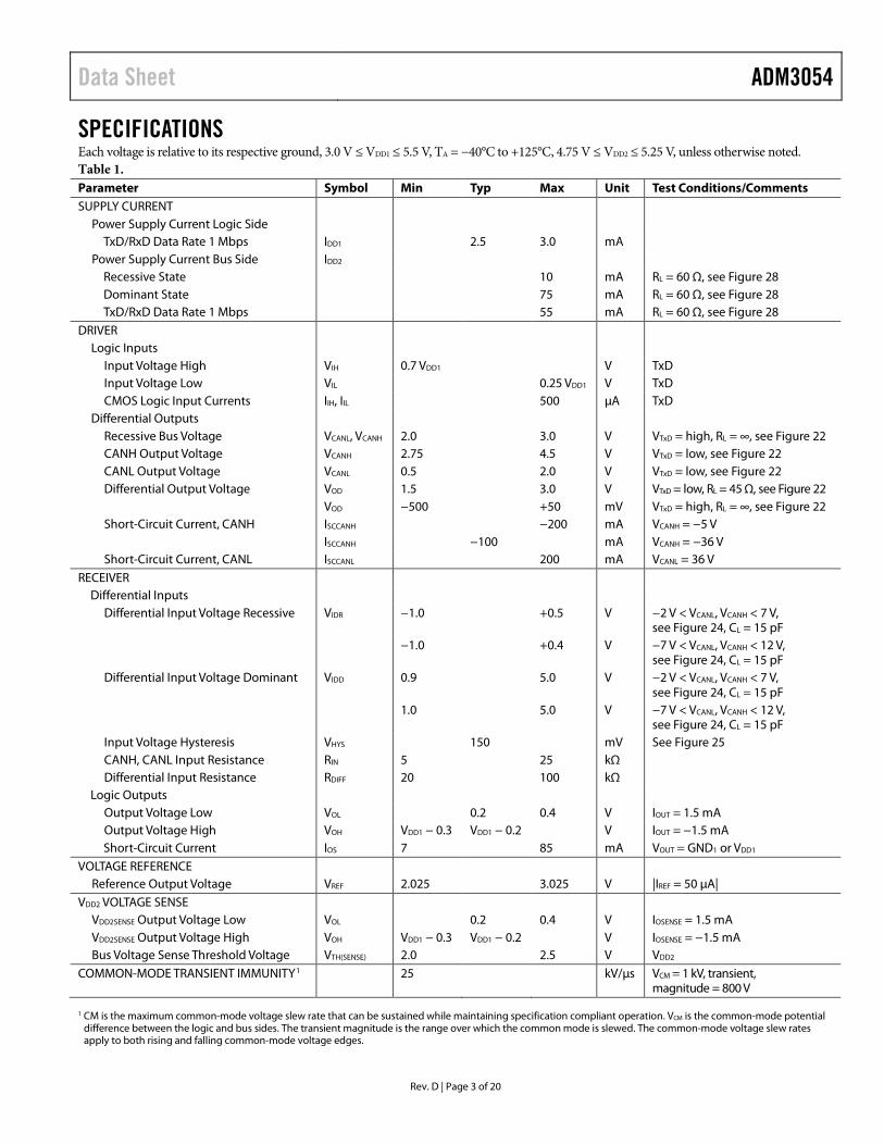
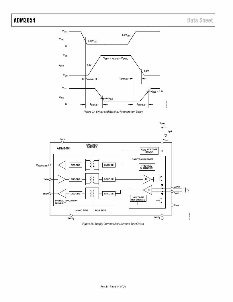
SPECIFICATIONS Each voltage is relative to its respective ground, 3.0 V ≤ VDD1 ≤ 5.5 V, TA = −40°C to +125°C, 4.75 V ≤ VDD2 ≤ 5.25 V, unless otherwise noted. Table 1. Parameter Symbol Min Typ Max Unit Test Conditions/Comments SUPPLY CURRENT
Power Supply Current Logic Side TxD/RxD Data Rate 1 Mbps IDD1 2.5 3.0 mA
Power Supply Current Bus Side IDD2 Recessive State 10 mA RL = 60 Ω, see Figure 28 Dominant State 75 mA RL = 60 Ω, see Figure 28 TxD/RxD Data Rate 1 Mbps 55 mA RL = 60 Ω, see Figure 28
DRIVER Logic Inputs
Input Voltage High VIH 0.7 VDD1 V TxD Input Voltage Low VIL 0.25 VDD1 V TxD CMOS Logic Input Currents IIH, IIL 500 µA TxD
Differential Outputs Recessive Bus Voltage VCANL, VCANH 2.0 3.0 V VTxD = high, RL = ∞, see Figure 22 CANH Output Voltage VCANH 2.75 4.5 V VTxD = low, see Figure 22 CANL Output Voltage VCANL 0.5 2.0 V VTxD = low, see Figure 22 Differential Output Voltage VOD 1.5 3.0 V VTxD = low, RL = 45 Ω, see Figure 22
VOD −500 +50 mV VTxD = high, RL = ∞, see Figure 22
Short-Circuit Current, CANH ISCCANH −200 mA VCANH = −5 V ISCCANH −100 mA VCANH = −36 V Short-Circuit Current, CANL ISCCANL 200 mA VCANL = 36 V
RECEIVER Differential Inputs
Differential Input Voltage Recessive VIDR −1.0 +0.5 V −2 V < VCANL, VCANH < 7 V, see Figure 24, CL = 15 pF
−1.0 +0.4 V −7 V < VCANL, VCANH < 12 V, see Figure 24, CL = 15 pF
Differential Input Voltage Dominant VIDD 0.9 5.0 V −2 V < VCANL, VCANH < 7 V, see Figure 24, CL = 15 pF
1.0 5.0 V −7 V < VCANL, VCANH < 12 V, see Figure 24, CL = 15 pF
Input Voltage Hysteresis VHYS 150 mV See Figure 25 CANH, CANL Input Resistance RIN 5 25 kΩ Differential Input Resistance RDIFF 20 100 kΩ
Logic Outputs Output Voltage Low VOL 0.2 0.4 V IOUT = 1.5 mA
Output Voltage High VOH VDD1 − 0.3 VDD1 − 0.2 V IOUT = −1.5 mA
Short-Circuit Current IOS 7 85 mA VOUT = GND1 or VDD1 VOLTAGE REFERENCE
Reference Output Voltage VREF 2.025 3.025 V |IREF = 50 µA| VDD2 VOLTAGE SENSE
VDD2SENSE Output Voltage Low VOL 0.2 0.4 V IOSENSE = 1.5 mA
VDD2SENSE Output Voltage High VOH VDD1 − 0.3 VDD1 − 0.2 V IOSENSE = −1.5 mA
Bus Voltage Sense Threshold Voltage VTH(SENSE) 2.0 2.5 V VDD2 COMMON-MODE TRANSIENT IMMUNITY1 25 kV/µs VCM = 1 kV, transient,
magnitude = 800 V 1 CM is the maximum common-mode voltage slew rate that can be sustained while maintaining specification compliant operation. VCM is the common-mode potential
difference between the logic and bus sides. The transient magnitude is the range over which the common mode is slewed. The common-mode voltage slew rates apply to both rising and falling common-mode voltage edges.
ADM3054 Data Sheet
Rev. D | Page 4 of 20
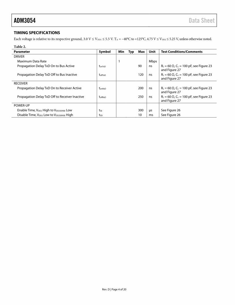
TIMING SPECIFICATIONS Each voltage is relative to its respective ground, 3.0 V ≤ VDD1 ≤ 5.5 V. TA = −40°C to +125°C, 4.75 V ≤ VDD2 ≤ 5.25 V, unless otherwise noted.
Table 2. Parameter Symbol Min Typ Max Unit Test Conditions/Comments DRIVER
Maximum Data Rate 1 Mbps Propagation Delay TxD On to Bus Active tonTxD 90 ns RL = 60 Ω, CL = 100 pF, see Figure 23
and Figure 27 Propagation Delay TxD Off to Bus Inactive toffTxD 120 ns RL = 60 Ω, CL = 100 pF, see Figure 23
and Figure 27 RECEIVER
Propagation Delay TxD On to Receiver Active tonRxD 200 ns RL = 60 Ω, CL = 100 pF, see Figure 23 and Figure 27
Propagation Delay TxD Off to Receiver Inactive toffRxD 250 ns RL = 60 Ω, CL = 100 pF, see Figure 23 and Figure 27
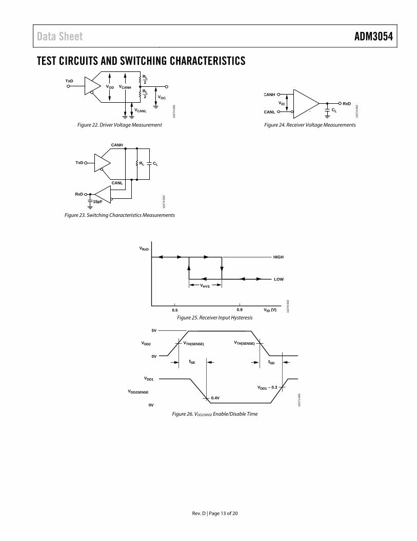
POWER-UP Enable Time, VDD2 High to VDD2SENSE Low tSE 300 µs See Figure 26 Disable Time, VDD2 Low to VDD2SENSE High tSD 10 ms See Figure 26
Data Sheet ADM3054
Rev. D | Page 5 of 20
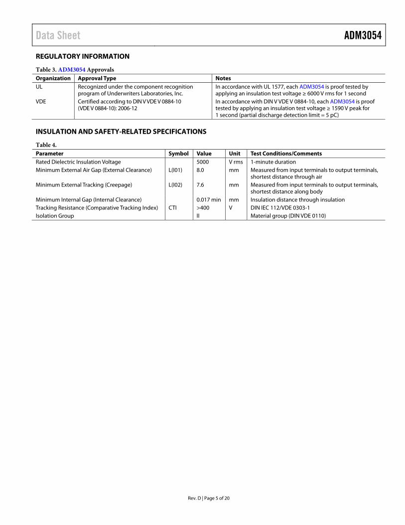
REGULATORY INFORMATION
Table 3. ADM3054 Approvals Organization Approval Type Notes UL Recognized under the component recognition
program of Underwriters Laboratories, Inc. In accordance with UL 1577, each ADM3054 is proof tested by applying an insulation test voltage ≥ 6000 V rms for 1 second
VDE Certified according to DIN V VDE V 0884-10 (VDE V 0884-10): 2006-12
In accordance with DIN V VDE V 0884-10, each ADM3054 is proof tested by applying an insulation test voltage ≥ 1590 V peak for 1 second (partial discharge detection limit = 5 pC)
INSULATION AND SAFETY-RELATED SPECIFICATIONS
Table 4. Parameter Symbol Value Unit Test Conditions/Comments Rated Dielectric Insulation Voltage 5000 V rms 1-minute duration Minimum External Air Gap (External Clearance) L(I01) 8.0 mm Measured from input terminals to output terminals,
shortest distance through air Minimum External Tracking (Creepage) L(I02) 7.6 mm Measured from input terminals to output terminals,
shortest distance along body Minimum Internal Gap (Internal Clearance) 0.017 min mm Insulation distance through insulation Tracking Resistance (Comparative Tracking Index) CTI >400 V DIN IEC 112/VDE 0303-1 Isolation Group II Material group (DIN VDE 0110)
ADM3054 Data Sheet
Rev. D | Page 6 of 20
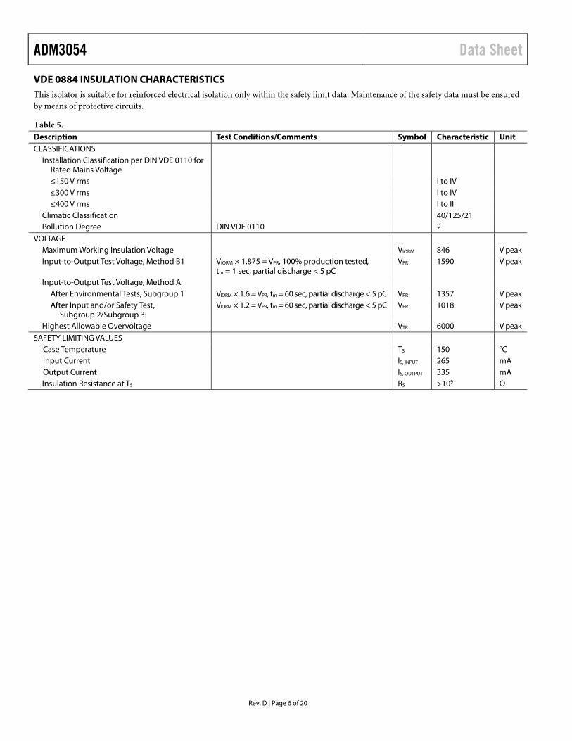
VDE 0884 INSULATION CHARACTERISTICS This isolator is suitable for reinforced electrical isolation only within the safety limit data. Maintenance of the safety data must be ensured by means of protective circuits.
Table 5. Description Test Conditions/Comments Symbol Characteristic Unit CLASSIFICATIONS
Installation Classification per DIN VDE 0110 for Rated Mains Voltage
≤150 V rms I to IV ≤300 V rms I to IV ≤400 V rms I to III
Climatic Classification 40/125/21 Pollution Degree DIN VDE 0110 2
VOLTAGE Maximum Working Insulation Voltage VIORM 846 V peak Input-to-Output Test Voltage, Method B1 VIORM × 1.875 = VPR, 100% production tested,
tm = 1 sec, partial discharge < 5 pC VPR 1590 V peak
Input-to-Output Test Voltage, Method A After Environmental Tests, Subgroup 1 VIORM × 1.6 = VPR, tm = 60 sec, partial discharge < 5 pC VPR 1357 V peak After Input and/or Safety Test,
Subgroup 2/Subgroup 3: VIORM × 1.2 = VPR, tm = 60 sec, partial discharge < 5 pC VPR 1018 V peak
Highest Allowable Overvoltage VTR 6000 V peak SAFETY LIMITING VALUES
Case Temperature TS 150 °C Input Current IS, INPUT 265 mA Output Current IS, OUTPUT 335 mA Insulation Resistance at TS RS >109 Ω
Data Sheet ADM3054
Rev. D | Page 7 of 20
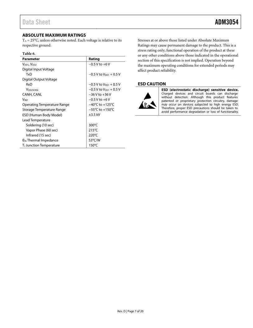
ABSOLUTE MAXIMUM RATINGS TA = 25°C, unless otherwise noted. Each voltage is relative to its respective ground.
Table 6. Parameter Rating VDD1, VDD2 −0.5 V to +6 V Digital Input Voltage
TxD −0.5 V to VDD1 + 0.5 V Digital Output Voltage
RxD −0.5 V to VDD1 + 0.5 V VDD2SENSE −0.5 V to VDD1 + 0.5 V
CANH, CANL −36 V to +36 V VREF −0.5 V to +6 V Operating Temperature Range −40°C to +125°C Storage Temperature Range −55°C to +150°C
ESD (Human Body Model) ±3.5 kV
Lead Temperature Soldering (10 sec) 300°C Vapor Phase (60 sec) 215°C Infrared (15 sec) 220°C
θJA Thermal Impedance 53°C/W TJ Junction Temperature 150°C
Stresses at or above those listed under Absolute Maximum Ratings may cause permanent damage to the product. This is a stress rating only; functional operation of the product at these or any other conditions above those indicated in the operational section of this specification is not implied. Operation beyond the maximum operating conditions for extended periods may affect product reliability.
ESD CAUTION
ADM3054 Data Sheet
Rev. D | Page 8 of 20
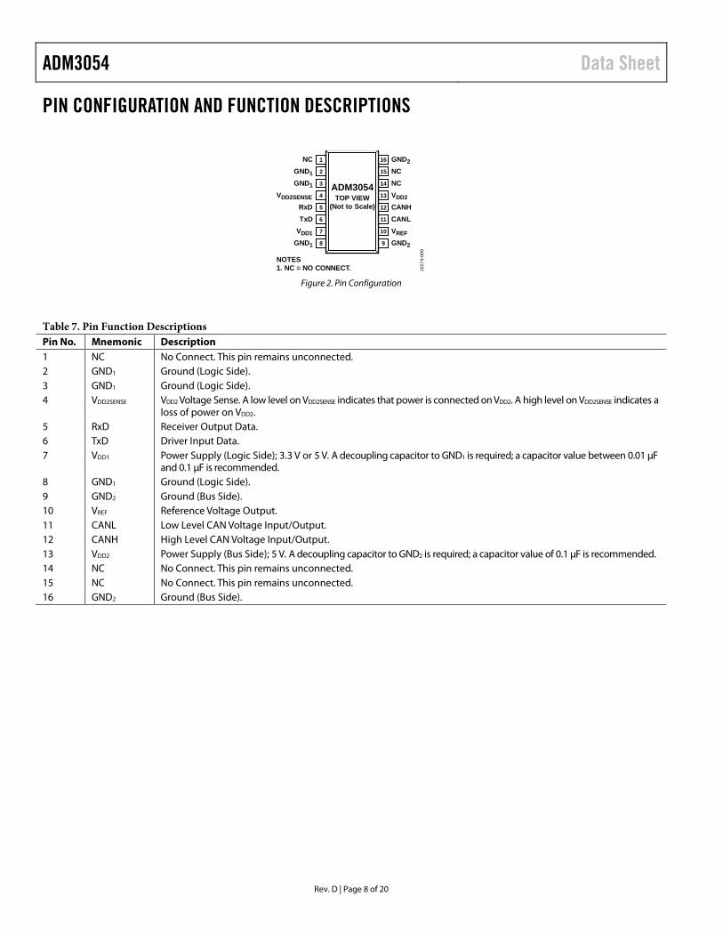
PIN CONFIGURATION AND FUNCTION DESCRIPTIONS
Figure 2. Pin Configuration
Table 7. Pin Function Descriptions Pin No. Mnemonic Description 1 NC No Connect. This pin remains unconnected. 2 GND1 Ground (Logic Side). 3 GND1 Ground (Logic Side). 4 VDD2SENSE VDD2 Voltage Sense. A low level on VDD2SENSE indicates that power is connected on VDD2. A high level on VDD2SENSE indicates a
loss of power on VDD2. 5 RxD Receiver Output Data. 6 TxD Driver Input Data. 7 VDD1 Power Supply (Logic Side); 3.3 V or 5 V. A decoupling capacitor to GND1 is required; a capacitor value between 0.01 µF
and 0.1 µF is recommended. 8 GND1 Ground (Logic Side). 9 GND2 Ground (Bus Side). 10 VREF Reference Voltage Output. 11 CANL Low Level CAN Voltage Input/Output. 12 CANH High Level CAN Voltage Input/Output. 13 VDD2 Power Supply (Bus Side); 5 V. A decoupling capacitor to GND2 is required; a capacitor value of 0.1 µF is recommended. 14 NC No Connect. This pin remains unconnected. 15 NC No Connect. This pin remains unconnected. 16 GND2 Ground (Bus Side).
NC 1
GND1 2
GND1 3
VDD2SENSE 4
GND216
NC15
NC14
VDD213
RxD 5 CANH12
TxD 6 CANL11
VDD1 7 VREF10
GND1 8 GND29
NOTES1. NC = NO CONNECT.
ADM3054TOP VIEW
(Not to Scale)
1027
4-00
9
Data Sheet ADM3054
Rev. D | Page 9 of 20
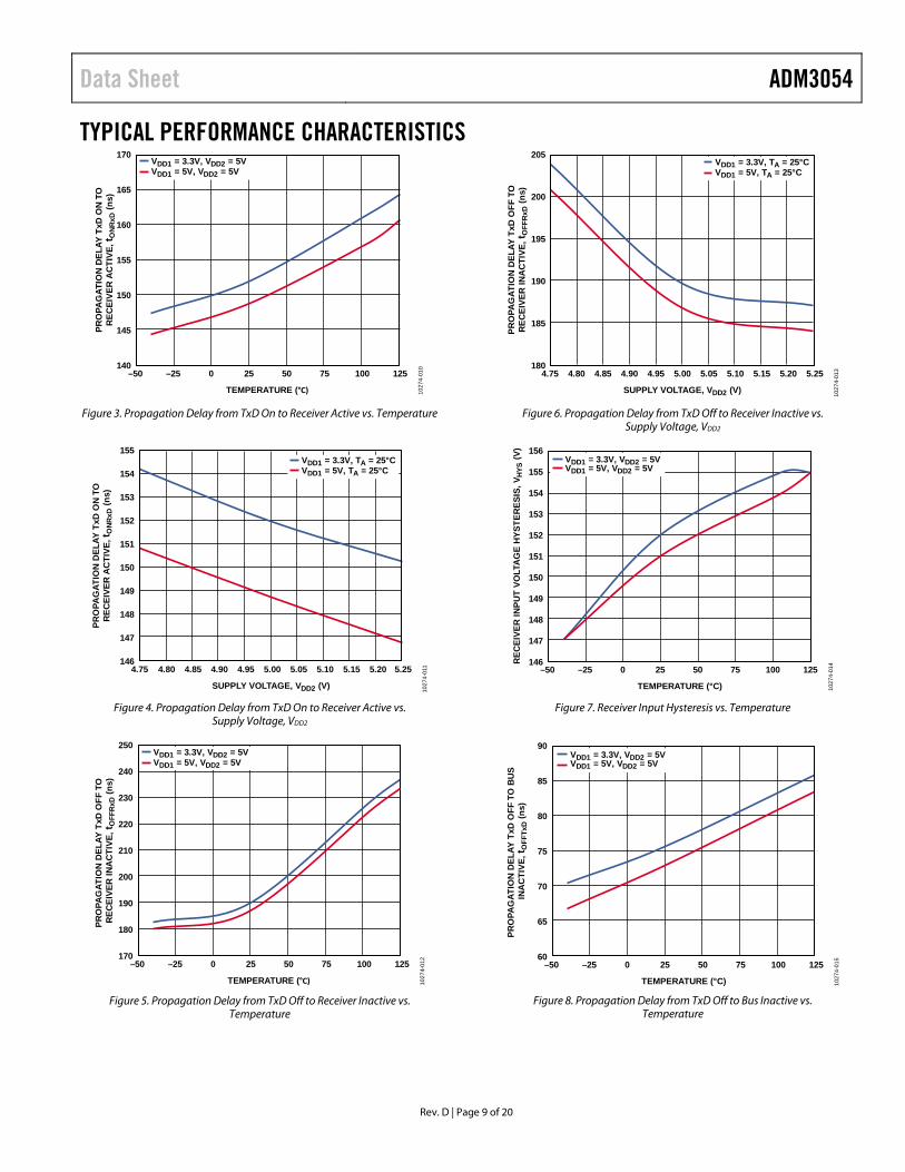
TYPICAL PERFORMANCE CHARACTERISTICS
Figure 3. Propagation Delay from TxD On to Receiver Active vs. Temperature
Figure 4. Propagation Delay from TxD On to Receiver Active vs.
Supply Voltage, VDD2
Figure 5. Propagation Delay from TxD Off to Receiver Inactive vs.
Temperature
Figure 6. Propagation Delay from TxD Off to Receiver Inactive vs.
Supply Voltage, VDD2
Figure 7. Receiver Input Hysteresis vs. Temperature
Figure 8. Propagation Delay from TxD Off to Bus Inactive vs.
Temperature
140
145
150
155
160
165
170
–50 –25 0 25 50 75 100 125
PRO
PAG
ATIO
N D
ELAY
TxD
ON
TOR
ECEI
VER
AC
TIVE
,tO
NR
xD (n
s)
TEMPERATURE (°C)
VDD1 = 3.3V, VDD2 = 5VVDD1 = 5V, VDD2 = 5V
1027
4-01
0
PRO
PAG
ATIO
N D
ELAY
TxD
ON
TOR
ECEI
VER
AC
TIVE
,tO
NR
xD (n
s)
146
147
148
149
150
151
152
153
154
155
4.75 4.80 4.85 4.90 4.95 5.00 5.05 5.10 5.15 5.20 5.25
SUPPLY VOLTAGE, VDD2 (V)
VDD1 = 3.3V, TA = 25°CVDD1 = 5V, TA = 25°C
1027
4-01
1
TEMPERATURE (°C)
170
180
190
200
210
220
230
240
250
–50 –25 0 25 50 75 100 125
PRO
PAG
ATIO
N D
ELAY
TxD
OFF
TOR
ECEI
VER
INA
CTI
VE,t
OFF
RxD
(ns)
VDD1 = 3.3V, VDD2 = 5VVDD1 = 5V, VDD2 = 5V
1027
4-01
2
180
185
190
195
200
205
4.75 4.80 4.85 4.90 4.95 5.00 5.05 5.10 5.15 5.20 5.25
PRO
PAG
ATIO
N D
ELA Y
TxD
OFF
TOR
ECEI
VER
INA
CTI
VE,t
OFF
RxD
(ns)
SUPPLY VOLTAGE, VDD2 (V)
VDD1 = 3.3V, TA = 25°CVDD1 = 5V, TA = 25°C
1027
4-01
3
146
147
148
149
150
151
152
153
154
155
156
–50 –25 0 25 50 75 100 125
REC
EIVE
R IN
PUT
VOLT
AG
E H
YSTE
RES
IS, V
HYS
(V)
TEMPERATURE (°C)
VDD1 = 3.3V, VDD2 = 5VVDD1 = 5V, VDD2 = 5V
1027
4-01
4
60
65
70
75
80
85
90
–50 –25 0 25 50 75 100 125
PRO
PAG
ATIO
N D
ELAY
TxD
OFF
TO B
US
INA
CTI
VE,t
OFF
TxD
(ns)
TEMPERATURE (°C)
VDD1 = 3.3V, VDD2 = 5VVDD1 = 5V, VDD2 = 5V
1027
4-01
5
ADM3054 Data Sheet
Rev. D | Page 10 of 20
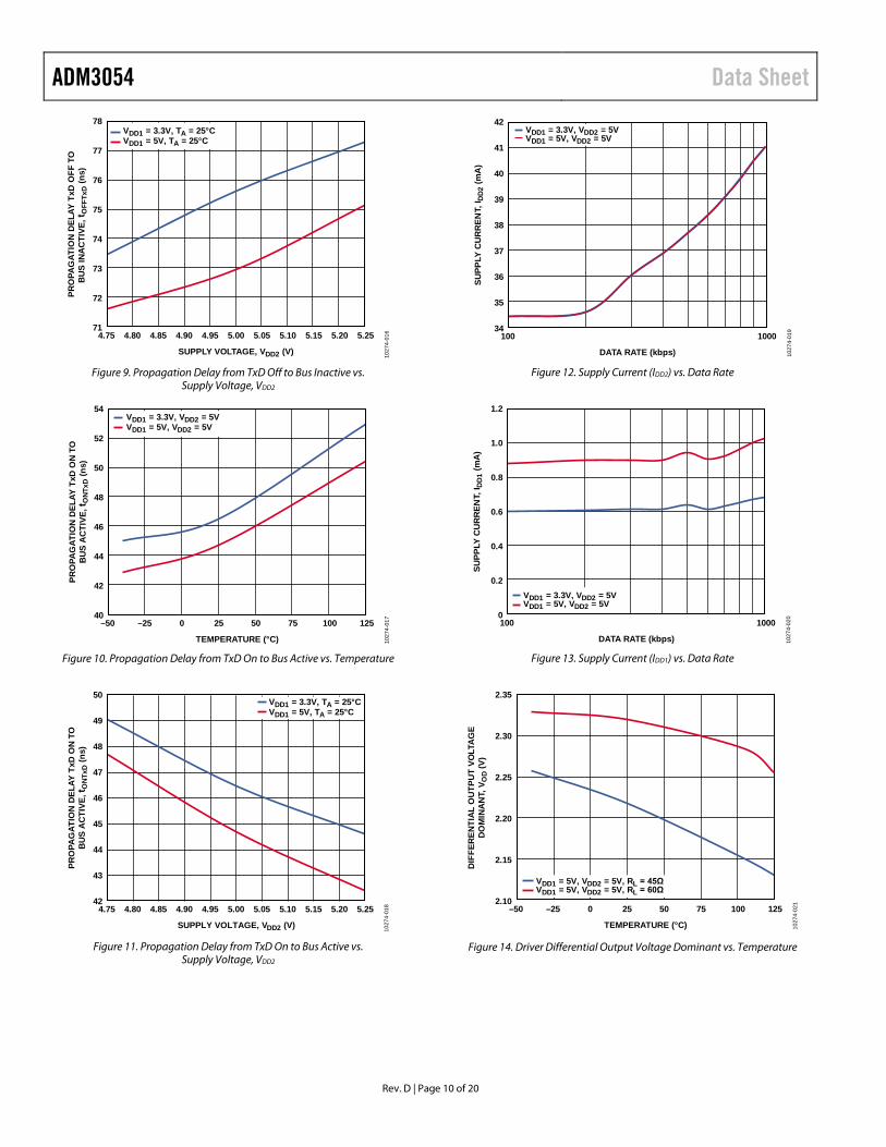
Figure 9. Propagation Delay from TxD Off to Bus Inactive vs.
Supply Voltage, VDD2
Figure 10. Propagation Delay from TxD On to Bus Active vs. Temperature
Figure 11. Propagation Delay from TxD On to Bus Active vs.
Supply Voltage, VDD2
Figure 12. Supply Current (IDD2) vs. Data Rate
Figure 13. Supply Current (IDD1) vs. Data Rate
Figure 14. Driver Differential Output Voltage Dominant vs. Temperature
71
72
73
74
75
76
77
78
4.75 4.80 4.85 4.90 4.95 5.00 5.05 5.10 5.15 5.20 5.25
PRO
PAG
ATIO
N D
ELAY
TxD
OFF
TOB
US
INA
CTI
VE,t
OFF
TxD
(ns)
SUPPLY VOLTAGE, VDD2 (V)
VDD1 = 3.3V, TA = 25°CVDD1 = 5V, TA = 25°C
1027
4-01
6
40
42
44
46
48
50
52
54
–50 –25 0 25 50 75 100 125
PRO
PAG
ATIO
N D
ELAY
TxD
ON
TOB
US
AC
TIVE
,tO
NTx
D (n
s)
TEMPERATURE (°C)
VDD1 = 3.3V, VDD2 = 5VVDD1 = 5V, VDD2 = 5V
1027
4-01
7
42
43
44
45
46
47
48
49
50
4.75 4.80 4.85 4.90 4.95 5.00 5.05 5.10 5.15 5.20 5.25
PRO
PAG
ATIO
N D
ELAY
TxD
ON
TOB
US
AC
TIVE
, tO
NTx
D (n
s)
VDD1 = 3.3V, TA = 25°CVDD1 = 5V, TA = 25°C
SUPPLY VOLTAGE, VDD2 (V)
1027
4-01
8
34
35
36
37
38
39
40
41
42
100 1000
SUPP
LY C
UR
REN
T, I D
D2
(mA
)
DATA RATE (kbps)
VDD1 = 3.3V, VDD2 = 5VVDD1 = 5V, VDD2 = 5V
1027
4-01
9
0
0.2
0.4
0.6
0.8
1.0
1.2
100 1000
SUPP
LY C
UR
REN
T, I D
D1
(mA
)
DATA RATE (kbps)
VDD1 = 3.3V, VDD2 = 5VVDD1 = 5V, VDD2 = 5V
1027
4-02
0
2.10
2.15
2.20
2.25
2.30
2.35
–50 –25 0 25 50 75 100 125
DIF
FER
ENTI
AL O
UTP
UT
VOLT
AG
ED
OM
INA
NT,
VO
D (V
)
TEMPERATURE (°C)
VDD1 = 5V, VDD2 = 5V, RL = 45ΩVDD1 = 5V, VDD2 = 5V, RL = 60Ω
1027
4-02
1
Data Sheet ADM3054
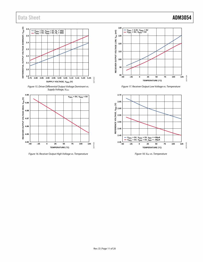
Rev. D | Page 11 of 20
Figure 15. Driver Differential Output Voltage Dominant vs.
Supply Voltage, VDD2
Figure 16. Receiver Output High Voltage vs. Temperature
Figure 17. Receiver Output Low Voltage vs. Temperature
Figure 18. VREF vs. Temperature
1.9
2.0
2.1
2.2
2.3
2.4
2.5
2.6
4.75 4.80 4.85 4.90 4.95 5.00 5.05 5.10 5.15 5.20 5.25DIF
FER
ENTI
AL O
UTP
UT
VOLT
AG
E D
OM
INA
NT,
VO
D (V
)
SUPPLY VOLTAGE, VDD2 (V)
VDD1 = 5V, VDD2 = 5V, RL = 45ΩVDD1 = 5V, VDD2 = 5V, RL = 60Ω
1027
4-02
2
4.84
4.85
4.86
4.87
4.88
4.89
4.90
–50 –25 0 25 50 75 100 125
REC
EIVE
R O
UTP
UT
VOLT
AG
E H
IGH
, VO
H(V
)
TEMPERATURE (°C)
VDD1 = 5V, VDD2 = 5V
1027
4-02
3
80
90
100
110
120
130
140
–50 –25 0 25 50 75 100 125
REC
EIVE
R O
UTP
UT
VOLT
AG
E LO
W, V
OL
(mV)
TEMPERATURE (°C)
VDD1 = 3.3V, VDD2 = 5VVDD1 = 5V, VDD2 = 5V
1027
4-02
4
TEMPERATURE (°C)
2.35
2.40
2.45
2.50
2.55
2.60
2.65
2.70
–50 –25 0 25 50 75 100 125
REF
EREN
CE
VOLT
AG
E, V
REF
(V)
VDD1 = 5V, VDD2 = 5V, IREF = +50μAVDD1 = 5V, VDD2 = 5V, IREF = –50μA
1027
4-02
5
ADM3054 Data Sheet
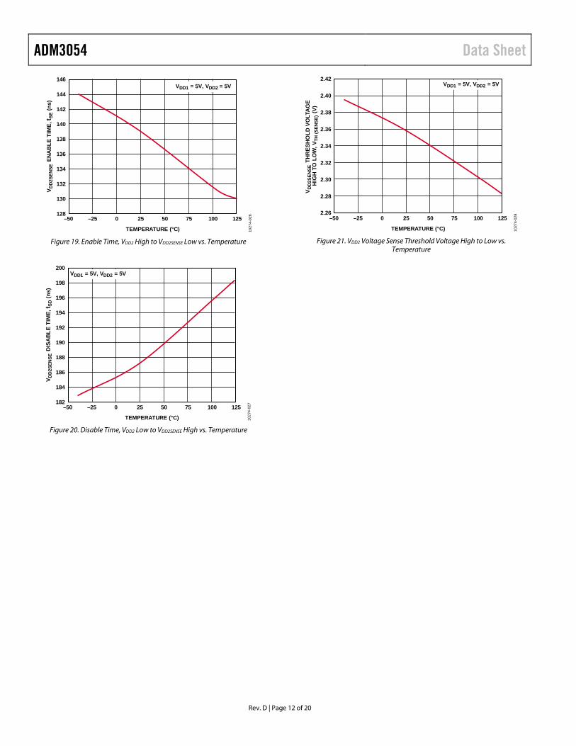
Rev. D | Page 12 of 20
Figure 19. Enable Time, VDD2 High to VDD2SENSE Low vs. Temperature
Figure 20. Disable Time, VDD2 Low to VDD2SENSE High vs. Temperature
Figure 21. VDD2 Voltage Sense Threshold Voltage High to Low vs.
Temperature
128
130
132
134
136
138
140
142
144
146
–50 –25 0 25 50 75 100 125
TEMPERATURE (°C)
V DD
2SEN
SE E
NA
BLE
TIM
E,t S
E (n
s)
VDD1 = 5V, VDD2 = 5V
1027
4-02
6
182
184
186
188
190
192
194
196
198
200
–50 –25 0 25 50 75 100 125
V DD
2SEN
SE D
ISA
BLE
TIM
E,t S
D (n
s)
VDD1 = 5V, VDD2 = 5V
TEMPERATURE (°C) 1027
4-02
7
2.26
2.28
2.30
2.32
2.34
2.36
2.38
2.40
2.42
–50 –25 0 25 50 75 100 125
V DD
2SEN
SE T
HR
ESH
OLD
VO
LTA
GE
HIG
HTO
LO
W, V
TH (S
ENSE
) (V)
VDD1 = 5V, VDD2 = 5V
TEMPERATURE (°C) 1027
4-02
8
Data Sheet ADM3054
Rev. D | Page 13 of 20
TEST CIRCUITS AND SWITCHING CHARACTERISTICS
Figure 22. Driver Voltage Measurement
Figure 23. Switching Characteristics Measurements
Figure 24. Receiver Voltage Measurements
Figure 25. Receiver Input Hysteresis
Figure 26. VDD2SENSE Enable/Disable Time
VOC
VOD
VCANL
VCANH
RL2
RL2
TxD
1027
4-00
6
CANH
CANL
TxD
RxD
CLRL
15pF
1027
4-00
3
CL
RxD
CANH
VID
CANL
1027
4-00
2
0.5 0.9
VRxD
HIGH
LOWVHYS
VID (V)
1027
4-00
4
VDD2SENSE
VTH(SENSE) VTH(SENSE)
tSE
0.4V
VDD1 – 0.3
tSD
0V
VDD1
1027
4-00
5
0V
5V
VDD2
ADM3054 Data Sheet
Rev. D | Page 14 of 20
Figure 27. Driver and Receiver Propagation Delay
Figure 28. Supply Current Measurement Test Circuit
0.25VDD1
0.9V
VOR
VOD
0V
0V
VDD1
0.5V
0.4VCC
VDIFF
VRxD
VDD1
VTxD
VDD1 – 0.3V
0.7VDD1
VDIFF = VCANH – VCANL
tONTxD tOFFTxD
tONRxD tOFFRxD
1027
4-00
7
TxD
RxD
ISOLATIONBARRIER
GND1
DECODE
DECODE
DECODE
VDD2SENSE ENCODE
ENCODE
ENCODE
VDD1
ADM3054
VOLTAGEREFERENCE
CAN TRANSCEIVER
LOGIC SIDE BUS SIDE
VDD2
VDD2
CANL
CANH
1µF
DIGITAL ISOLATIONiCoupler®
R
D
VDD2 VOLTAGESENSE
THERMALSHUTDOWN
GND2
VREF
RL10
274-
008
Data Sheet ADM3054
Rev. D | Page 15 of 20
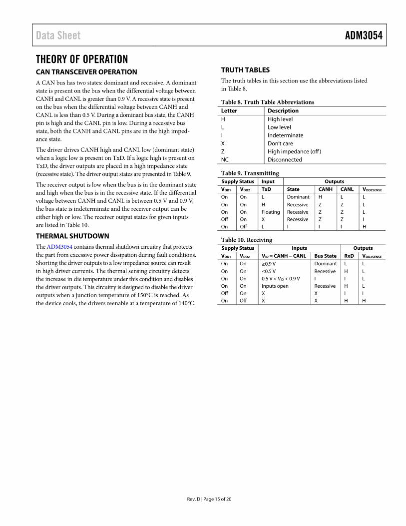
THEORY OF OPERATION CAN TRANSCEIVER OPERATION A CAN bus has two states: dominant and recessive. A dominant state is present on the bus when the differential voltage between CANH and CANL is greater than 0.9 V. A recessive state is present on the bus when the differential voltage between CANH and CANL is less than 0.5 V. During a dominant bus state, the CANH pin is high and the CANL pin is low. During a recessive bus state, both the CANH and CANL pins are in the high imped-ance state.
The driver drives CANH high and CANL low (dominant state) when a logic low is present on TxD. If a logic high is present on TxD, the driver outputs are placed in a high impedance state (recessive state). The driver output states are presented in Table 9.
The receiver output is low when the bus is in the dominant state and high when the bus is in the recessive state. If the differential voltage between CANH and CANL is between 0.5 V and 0.9 V, the bus state is indeterminate and the receiver output can be either high or low. The receiver output states for given inputs are listed in Table 10.
THERMAL SHUTDOWN The ADM3054 contains thermal shutdown circuitry that protects the part from excessive power dissipation during fault conditions. Shorting the driver outputs to a low impedance source can result in high driver currents. The thermal sensing circuitry detects the increase in die temperature under this condition and disables the driver outputs. This circuitry is designed to disable the driver outputs when a junction temperature of 150°C is reached. As the device cools, the drivers reenable at a temperature of 140°C.
TRUTH TABLES The truth tables in this section use the abbreviations listed in Table 8.
Table 8. Truth Table Abbreviations Letter Description H High level L Low level I Indeterminate X Don’t care Z High impedance (off ) NC Disconnected
Table 9. Transmitting Supply Status Input Outputs
VDD1 VDD2 TxD State CANH CANL VDD2SENSE On On L Dominant H L L
On On H Recessive Z Z L On On Floating Recessive Z Z L Off On X Recessive Z Z I On Off L I I I H
Table 10. Receiving Supply Status Inputs Outputs
VDD1 VDD2 VID = CANH − CANL Bus State RxD VDD2SENSE On On ≥0.9 V Dominant L L
On On ≤0.5 V Recessive H L On On 0.5 V < VID < 0.9 V I I L On On Inputs open Recessive H L Off On X X I I On Off X X H H
ADM3054 Data Sheet
Rev. D | Page 16 of 20
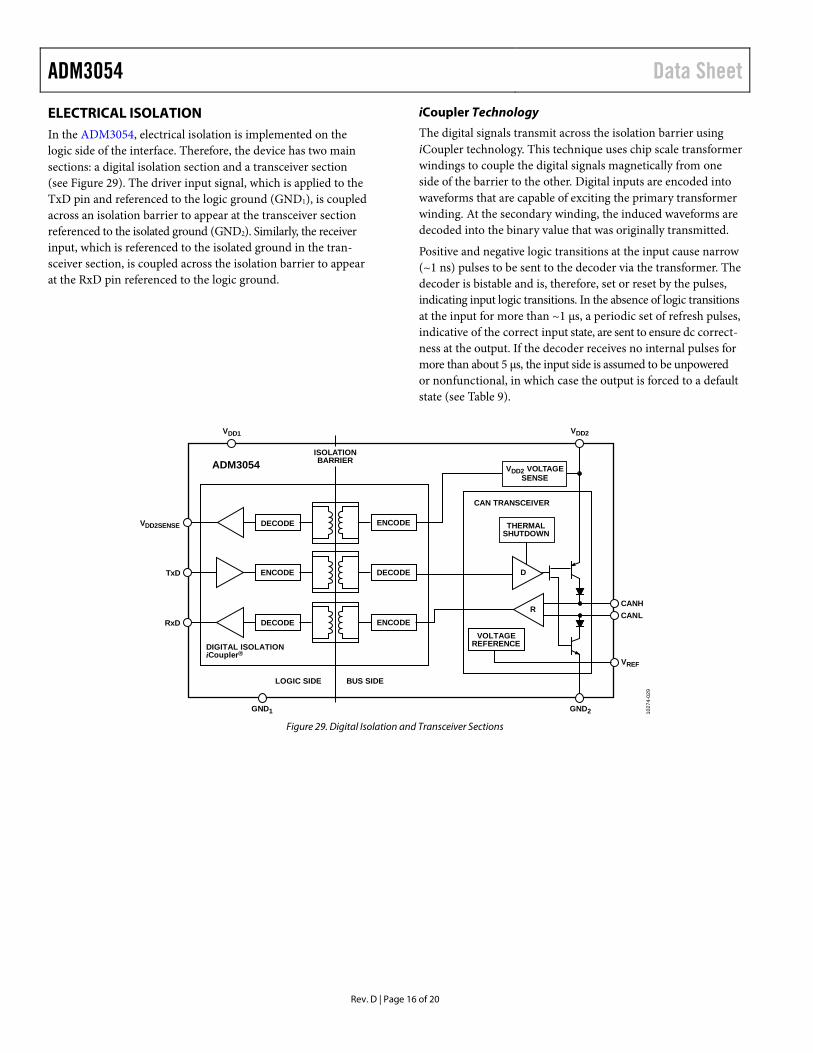
ELECTRICAL ISOLATION In the ADM3054, electrical isolation is implemented on the logic side of the interface. Therefore, the device has two main sections: a digital isolation section and a transceiver section (see Figure 29). The driver input signal, which is applied to the TxD pin and referenced to the logic ground (GND1), is coupled across an isolation barrier to appear at the transceiver section referenced to the isolated ground (GND2). Similarly, the receiver input, which is referenced to the isolated ground in the tran-sceiver section, is coupled across the isolation barrier to appear at the RxD pin referenced to the logic ground.
iCoupler Technology
The digital signals transmit across the isolation barrier using iCoupler technology. This technique uses chip scale transformer windings to couple the digital signals magnetically from one side of the barrier to the other. Digital inputs are encoded into waveforms that are capable of exciting the primary transformer winding. At the secondary winding, the induced waveforms are decoded into the binary value that was originally transmitted.
Positive and negative logic transitions at the input cause narrow (~1 ns) pulses to be sent to the decoder via the transformer. The decoder is bistable and is, therefore, set or reset by the pulses, indicating input logic transitions. In the absence of logic transitions at the input for more than ~1 μs, a periodic set of refresh pulses, indicative of the correct input state, are sent to ensure dc correct-ness at the output. If the decoder receives no internal pulses for more than about 5 μs, the input side is assumed to be unpowered or nonfunctional, in which case the output is forced to a default state (see Table 9).
Figure 29. Digital Isolation and Transceiver Sections
TxD
RxD
ISOLATIONBARRIER
GND1
DECODE
DECODE
DECODE
VDD2SENSE ENCODE
ENCODE
ENCODE
VREF
VDD1
ADM3054
VOLTAGEREFERENCE
CAN TRANSCEIVER
LOGIC SIDE BUS SIDE
VDD2
CANLCANH
DIGITAL ISOLATIONiCoupler®
R
D
VDD2 VOLTAGESENSE
THERMALSHUTDOWN
GND2 1027
4-02
9
Data Sheet ADM3054
Rev. D | Page 17 of 20
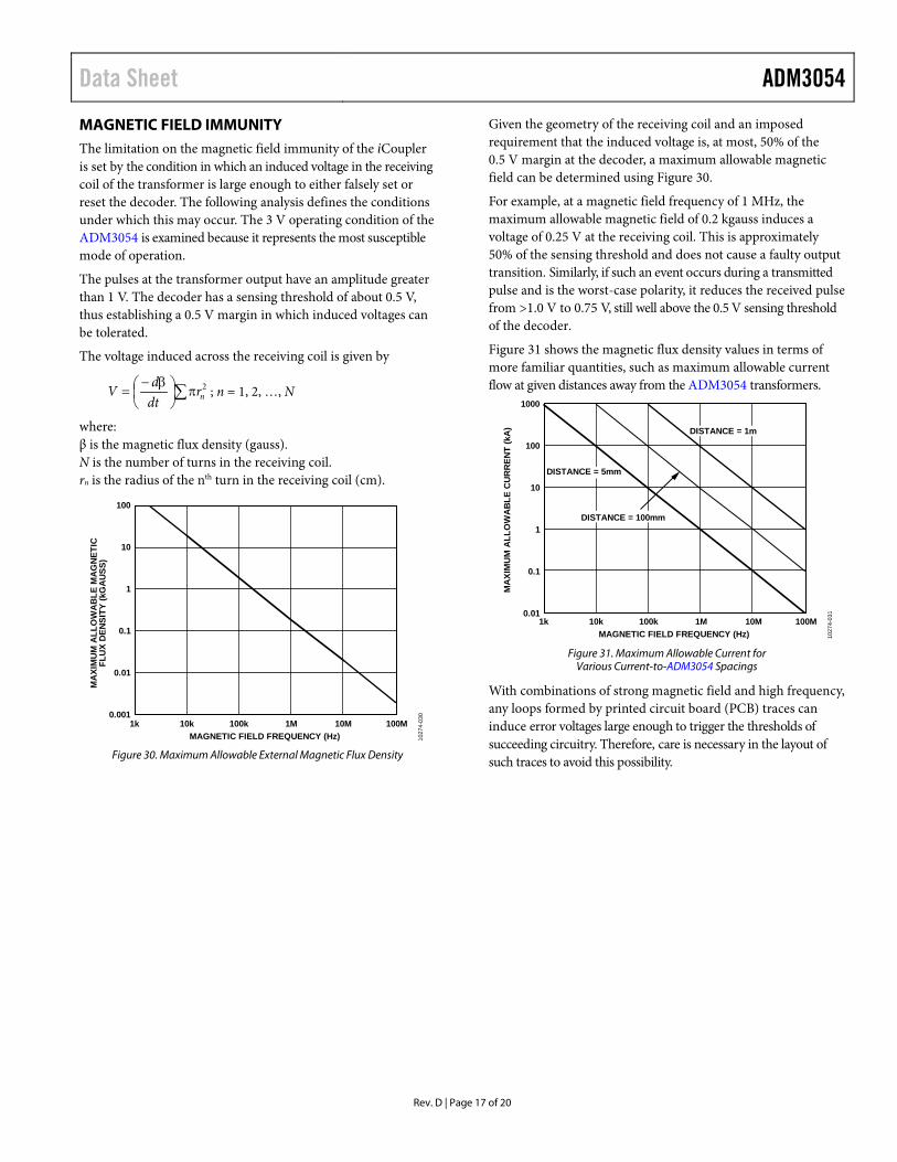
MAGNETIC FIELD IMMUNITY The limitation on the magnetic field immunity of the iCoupler is set by the condition in which an induced voltage in the receiving coil of the transformer is large enough to either falsely set or reset the decoder. The following analysis defines the conditions under which this may occur. The 3 V operating condition of the ADM3054 is examined because it represents the most susceptible mode of operation.
The pulses at the transformer output have an amplitude greater than 1 V. The decoder has a sensing threshold of about 0.5 V, thus establishing a 0.5 V margin in which induced voltages can be tolerated.
The voltage induced across the receiving coil is given by
∑π
β−
= 2nrdt
dV ; n = 1, 2, …, N
where: β is the magnetic flux density (gauss). N is the number of turns in the receiving coil. rn is the radius of the nth turn in the receiving coil (cm).
Figure 30. Maximum Allowable External Magnetic Flux Density
Given the geometry of the receiving coil and an imposed requirement that the induced voltage is, at most, 50% of the 0.5 V margin at the decoder, a maximum allowable magnetic field can be determined using Figure 30.
For example, at a magnetic field frequency of 1 MHz, the maximum allowable magnetic field of 0.2 kgauss induces a voltage of 0.25 V at the receiving coil. This is approximately 50% of the sensing threshold and does not cause a faulty output transition. Similarly, if such an event occurs during a transmitted pulse and is the worst-case polarity, it reduces the received pulse from >1.0 V to 0.75 V, still well above the 0.5 V sensing threshold of the decoder.
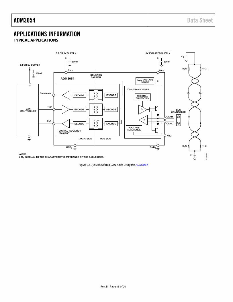
Figure 31 shows the magnetic flux density values in terms of more familiar quantities, such as maximum allowable current flow at given distances away from the ADM3054 transformers.
Figure 31. Maximum Allowable Current for
Various Current-to-ADM3054 Spacings
With combinations of strong magnetic field and high frequency, any loops formed by printed circuit board (PCB) traces can induce error voltages large enough to trigger the thresholds of succeeding circuitry. Therefore, care is necessary in the layout of such traces to avoid this possibility.
MAGNETIC FIELD FREQUENCY (Hz)1k 10k 100k 100M1M 10M
100
10
1
0.1
0.01
0.001
MA
XIM
UM
ALL
OW
AB
LE M
AG
NET
ICFL
UX
DEN
SITY
(kG
AU
SS)
1027
4-03
0
MAGNETIC FIELD FREQUENCY (Hz)1k 10k 100k 100M1M 10M
DISTANCE = 1m
DISTANCE = 100mm
DISTANCE = 5mm
1000
100
0.1
1
10
0.01
MA
XIM
UM
ALL
OW
AB
LE C
UR
REN
T (k
A)
1027
4-03
1
ADM3054 Data Sheet
Rev. D | Page 18 of 20
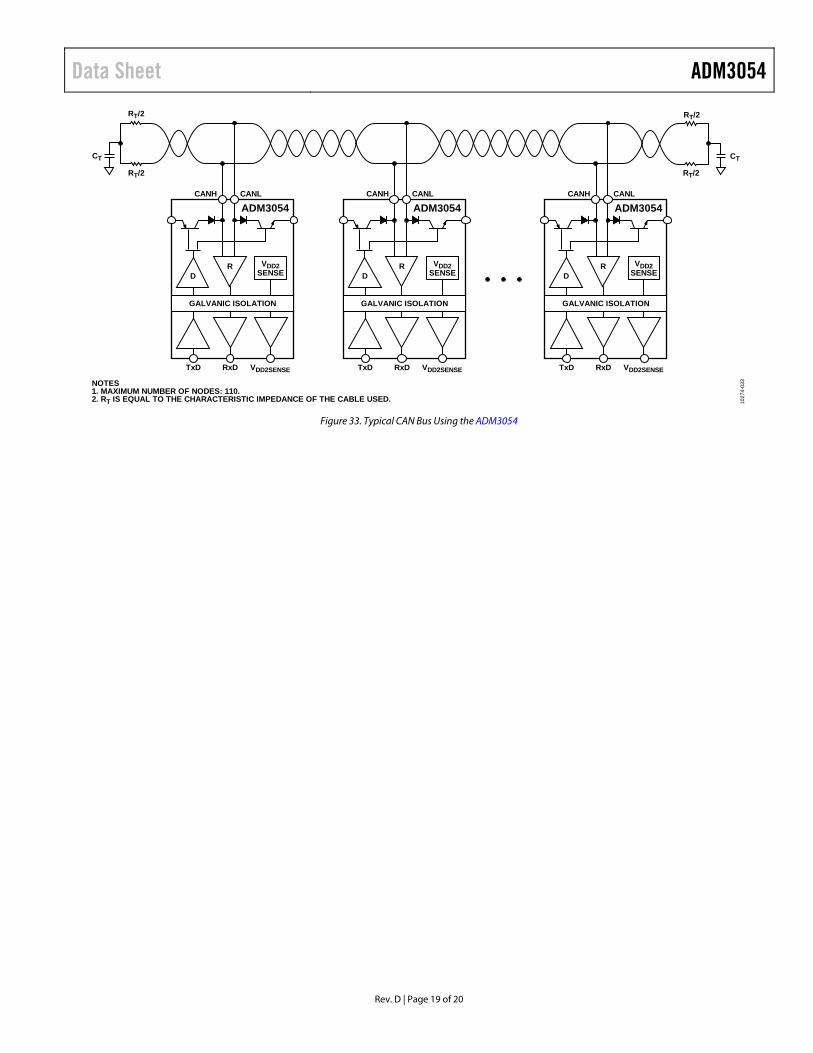
APPLICATIONS INFORMATION TYPICAL APPLICATIONS
Figure 32. Typical Isolated CAN Node Using the ADM3054
GND1
TxD
RxD
ISOLATIONBARRIER
DECODE
DECODE
VDD2SENSE
ENCODE
VDD1
ADM3054
VOLTAGEREFERENCE
CAN TRANSCEIVER
LOGIC SIDE
NOTES1. RT iS EQUAL TO THE CHARACTERISTIC IMPEDANCE OF THE CABLE USED.
BUS SIDE
VDD2
CANL
CANH
BUSCONNECTOR
100nF
DIGITAL ISOLATIONiCoupler®
R
D
VDD2 VOLTAGESENSE
THERMALSHUTDOWN
GND2
3.3 OR 5V SUPPLY 5V ISOLATED SUPPLY
100nF
VREF
3.3 OR 5V SUPPLY
CANCONTROLLER
100nF
CT
RT/2 RT/2
RT/2 RT/2
CT
DECODE
ENCODE
ENCODE
1027
4-03
2
Data Sheet ADM3054
Rev. D | Page 19 of 20
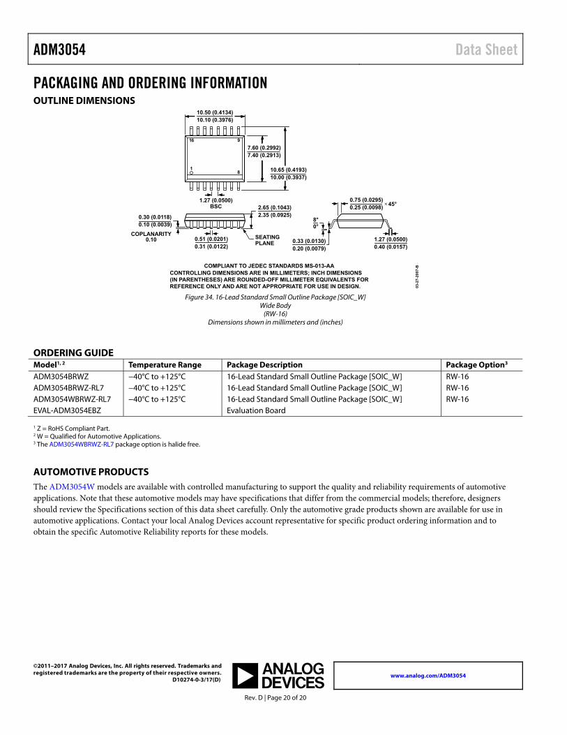
Figure 33. Typical CAN Bus Using the ADM3054
VDD2SENSE
VDD2SENSERxDTxD
ADM3054
RD
CT CT
RT/2
RT/2
RT/2
RT/2
GALVANIC ISOLATION
CANH CANL
VDD2SENSE
VDD2SENSERxDTxD
ADM3054
RD
GALVANIC ISOLATION
NOTES1. MAXIMUM NUMBER OF NODES: 110.2. RT IS EQUAL TO THE CHARACTERISTIC IMPEDANCE OF THE CABLE USED.
CANH CANL
VDD2SENSE
VDD2SENSERxDTxD
ADM3054
RD
GALVANIC ISOLATION
CANH CANL
1027
4-03
3
ADM3054 Data Sheet
Rev. D | Page 20 of 20
PACKAGING AND ORDERING INFORMATION OUTLINE DIMENSIONS
Figure 34. 16-Lead Standard Small Outline Package [SOIC_W]
Wide Body (RW-16)
Dimensions shown in millimeters and (inches)
ORDERING GUIDE Model1, 2 Temperature Range Package Description Package Option3 ADM3054BRWZ −40°C to +125°C 16-Lead Standard Small Outline Package [SOIC_W] RW-16 ADM3054BRWZ-RL7 −40°C to +125°C 16-Lead Standard Small Outline Package [SOIC_W] RW-16 ADM3054WBRWZ-RL7 −40°C to +125°C 16-Lead Standard Small Outline Package [SOIC_W] RW-16 EVAL-ADM3054EBZ Evaluation Board 1 Z = RoHS Compliant Part. 2 W = Qualified for Automotive Applications. 3 The ADM3054WBRWZ-RL7 package option is halide free.
AUTOMOTIVE PRODUCTS The ADM3054W models are available with controlled manufacturing to support the quality and reliability requirements of automotive applications. Note that these automotive models may have specifications that differ from the commercial models; therefore, designers should review the Specifications section of this data sheet carefully. Only the automotive grade products shown are available for use in automotive applications. Contact your local Analog Devices account representative for specific product ordering information and to obtain the specific Automotive Reliability reports for these models.
CONTROLLING DIMENSIONS ARE IN MILLIMETERS; INCH DIMENSIONS(IN PARENTHESES) ARE ROUNDED-OFF MILLIMETER EQUIVALENTS FORREFERENCE ONLY AND ARE NOT APPROPRIATE FOR USE IN DESIGN.
COMPLIANT TO JEDEC STANDARDS MS-013-AA
10.50 (0.4134)10.10 (0.3976)
0.30 (0.0118)0.10 (0.0039)
2.65 (0.1043)2.35 (0.0925)
10.65 (0.4193)10.00 (0.3937)
7.60 (0.2992)7.40 (0.2913)
0.75 (0.0295)0.25 (0.0098)
45°
1.27 (0.0500)0.40 (0.0157)
COPLANARITY0.10 0.33 (0.0130)
0.20 (0.0079)
0.51 (0.0201)0.31 (0.0122)
SEATINGPLANE
8°0°
16 9
81
1.27 (0.0500)BSC
03-2
7-2
007
-B
©2011–2017 Analog Devices, Inc. All rights reserved. Trademarks and registered trademarks are the property of their respective owners.
D10274-0-3/17(D) www.analog.com/ADM3054