Embed Size (px)
Citation preview

November 2008 Rev 7 1/15
15
STGD5NB120SZ
5 A - 1200 V - low drop internally clamped IGBT
Features Low on-voltage drop (VCE(sat))
High current capability
Off losses include tail current
High voltage clamping
Applications Light dimmer
Inrush current limitation
Pre-heating for electronic lamp ballast
DescriptionThis IGBT utilizes the advanced Power MESH™ process resulting in an excellent trade-off between switching performance and low on-state behavior.
Figure 1. Internal schematic diagram
1
3
DPAK IPAK
32
1
Table 1. Device summary
Order codes Marking Package Packaging
STGD5NB120SZ-1 GD5NB120SZ IPAK Tube
STGD5NB120SZT4 GD5NB120SZ DPAK Tape and reel
www.st.com

Contents STGD5NB120SZ
2/15
Contents
1 Electrical ratings . . . . . . . . . . . . . . . . . . . . . . . . . . . . . . . . . . . . . . . . . . . . 3
2 Electrical characteristics . . . . . . . . . . . . . . . . . . . . . . . . . . . . . . . . . . . . . 42.1 Electrical characteristics (curves) . . . . . . . . . . . . . . . . . . . . . . . . . . . . . 6
3 Test circuit . . . . . . . . . . . . . . . . . . . . . . . . . . . . . . . . . . . . . . . . . . . . . . . . 9
4 Package mechanical data . . . . . . . . . . . . . . . . . . . . . . . . . . . . . . . . . . . . 10
5 Packaging mechanical data . . . . . . . . . . . . . . . . . . . . . . . . . . . . . . . . . 13
6 Revision history . . . . . . . . . . . . . . . . . . . . . . . . . . . . . . . . . . . . . . . . . . . 14

STGD5NB120SZ Electrical ratings
3/15
1 Electrical ratings
Table 2. Absolute maximum ratings
Symbol Parameter Value Unit
VCES Collector-emitter voltage (VGE = 0) 1200 V
IC(1)
1. Calculated according to the iterative formula:
Collector current (continuous) at TC = 25 °C 10 A
IC(1) Collector current (continuous) at TC = 100 °C 5 A
ICP(2)
2. Pulse width limited by max. temperature allowed
Pulsed collector current 10 A
ICL (3)
3. VCLAMP = 80% (VCES), VGE = 15 V, RG = 10 Ω, TJ = 150 °C
Turn-off latching current 10 A
VGE Gate-emitter voltage ±20 V
VECR Emitter-collector voltage 20 V
EAS (4)
4. VCE = 50 V , IAV = 3.3 A
Single pulse avalanche energy at TC = 25 °C 10 mJ
Single pulse avalanche energy at TC = 100 °C 7 mJ
PTOT Total dissipation at TC = 25 °C 75 W
Tj Operating junction temperature – 55 to 150 °C
Table 3. Thermal resistance
Symbol Parameter Value Unit
Rthj-case Thermal resistance junction-case IGBT max 1.67 °C/W
Rthj-amb Thermal resistance junction-ambient max 100 °C/W
IC TC( )Tj max( ) TC–
Rthj c– VCE sat( ) max( ) Tj max( ) IC TC( ),( )×-------------------------------------------------------------------------------------------------------=

Electrical characteristics STGD5NB120SZ
4/15
2 Electrical characteristics
(TCASE=25 °C unless otherwise specified)
Table 4. Static electrical characteristics
Symbol Parameter Test conditions Min. Typ. Max. Unit
V(BR)CES
Collector-emitter breakdown voltage
(VGE = 0)IC = 10 mA 1200 V
VCE(sat)Collector-emitter saturation voltage
VGE = 15 V, IC= 5 A
VGE= 15 V, IC= 5 A,TC = 125 °C
1.3
1.2
2.0 V
V
VGE(th) Gate threshold voltage VCE= VGE, IC= 250 µA 2 5 V
VGE Gate emitter voltageVCE= 2.5 V, IC= 2 A,
TC = 25 ÷ 125 °C6.5 V
ICESCollector cut-off current
(VGE = 0)
VCE = 900 V
VCE = 900 VTC= 125 °C
50
250
µA
µA
IGESGate-emitter leakagecurrent (VCE = 0)
VGE = ±20 V ±100 nA
gfs Forward transconductance VCE = 15 V, IC= 5 A 5 S
RG Gate resistance 4 kΩ
Table 5. Dynamic electrical characteristics
Symbol Parameter Test conditions Min. Typ. Max. Unit
Cies
Coes
Cres
Input capacitanceOutput capacitance
Reverse transfer capacitance
VCE = 25 V, f = 1 MHz,
VGE = 0
430
40
7
pF
pF
pF

STGD5NB120SZ Electrical characteristics
5/15
Table 6. Switching on/off (inductive load)
Symbol Parameter Test conditions Min. Typ. Max. Unit
td(on)
tr(di/dt)on
Turn-on delay time
Current rise time
Turn-on current slope
VCC = 960 V, IC = 5A
Rdrive= 1 kΩ, VGE = 15 V,
(see Figure 18)
690
170
39.6
ns
ns
A/µs
td(on)
tr(di/dt)on
Turn-on delay time Current rise time
Turn-on current slope
VCC = 960 V, IC = 5A
Rdrive= 1 kΩ, VGE = 15 V
TC = 125 °C (see Figure 18)
600185
39
nsns
A/µs
tctr(Voff)
td(off)
tf
Cross-over time
Off voltage rise time
Turn-off delay timeCurrent fall time
VCC = 960 V, IC = 5A
Rdrive= 1 kΩ, VGE = 15 V
(see Figure 18)
4
2.2
12.11.13
µs
µs
µsµs
tctr(Voff)
td(off)
tf
Cross-over time
Off voltage rise timeTurn-off delay time
Current fall time
VCC = 960 V, IC = 5A
Rdrive= 1 kΩ, VGE = 15 V,
TC = 125 °C (see Figure 18)
5
2.212.1
2
µs
µsµs
µs
Table 7. Switching energy (inductive load)
Symbol Parameter Test conditions Min. Typ. Max. Unit
Eon (1)
Eoff(2)
Ets
1. Eon is the turn-on losses when a typical diode is used in the test circuit in (see Figure 18). If the IGBT is offered in a package with a co-pak diode, the co-pack diode is used as external diode. IGBTs & Diode are at the same temperature (25°C and 125°C)
2. Turn-off losses include also the tail of the collector current
Turn-on switching losses
Turn-off switching losses
Total switching losses
VCC = 960 V, IC = 5A
Rdrive= 1 kΩ, VGE = 15 V
(see Figure 18)
2.59
9
11.59
mJ
mJ
mJ
Eon (1)
Eoff(2)
Ets
Turn-on switching lossesTurn-off switching losses
Total switching losses
VCC = 960 V, IC = 5A
Rdrive= 1 kΩ, VGE = 15 V,
TC = 125 °C (see Figure 18)
2.6410.2
12.68
mJmJ
mJ
Table 8. Functional test
Symbol Parameter Test conditions Min. Typ. Max. Unit
IASUnclamped inductive switching current
VCC = 50 V, L = 1.8 mH
Tstart = 25 °C, Rdrive= 1 kΩ3.3 A
Electrical characteristics STGD5NB120SZ
6/15
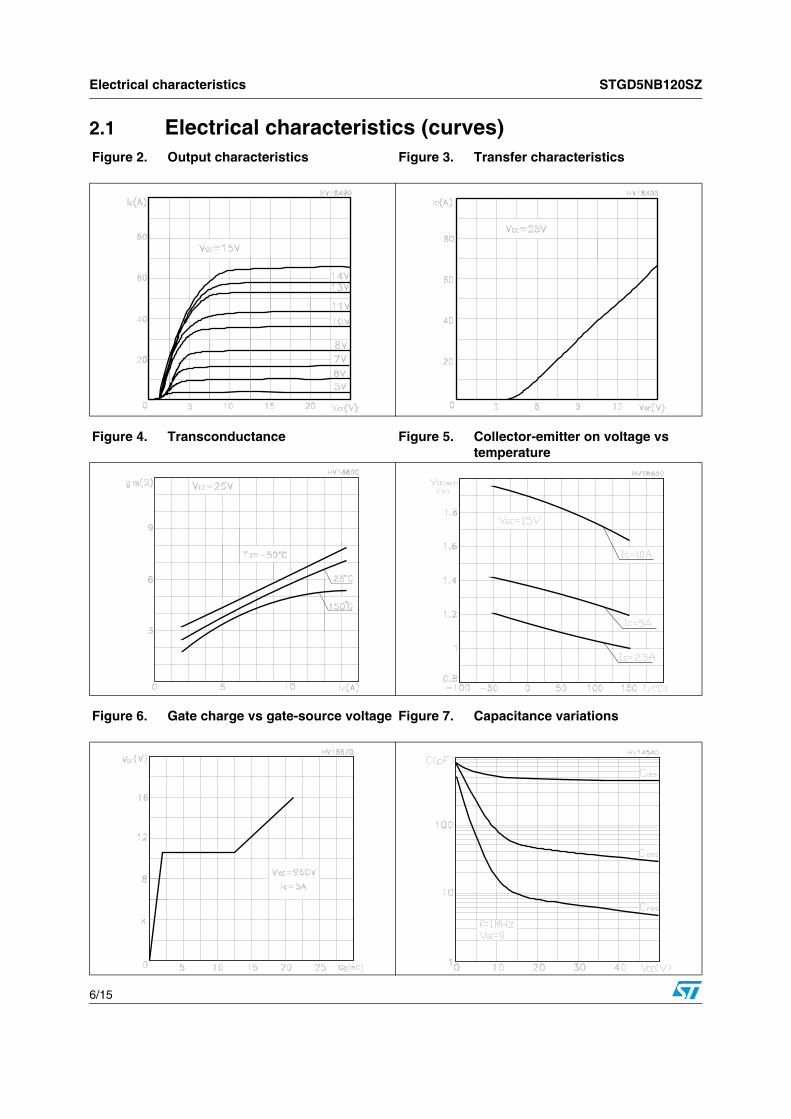
2.1 Electrical characteristics (curves) Figure 2. Output characteristics Figure 3. Transfer characteristics
Figure 4. Transconductance Figure 5. Collector-emitter on voltage vs temperature
Figure 6. Gate charge vs gate-source voltage Figure 7. Capacitance variations
STGD5NB120SZ Electrical characteristics
7/15
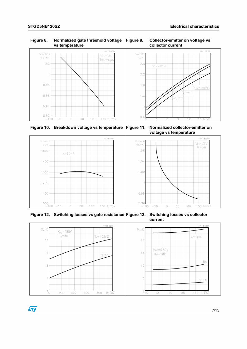
Figure 8. Normalized gate threshold voltage vs temperature
Figure 9. Collector-emitter on voltage vs collector current
Figure 10. Breakdown voltage vs temperature Figure 11. Normalized collector-emitter on voltage vs temperature
Figure 12. Switching losses vs gate resistance Figure 13. Switching losses vs collector current
Electrical characteristics STGD5NB120SZ
8/15
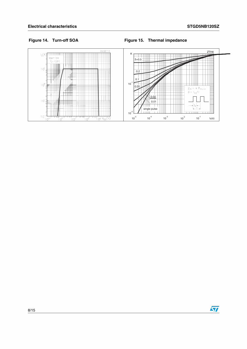
Figure 14. Turn-off SOA Figure 15. Thermal impedance
10
K
δ=0.5
0.2
0.1
0.05
single pulse
0.01
0.02
-2
10-1
10-5
10-4
10-3
10-2
10-1
tp(s)
ZTH4

STGD5NB120SZ Test circuit
9/15
3 Test circuit
Figure 16. Test circuit for inductive load switching
Figure 17. Gate charge test circuit
Figure 18. Switching waveform
Package mechanical data STGD5NB120SZ
10/15
4 Package mechanical data
In order to meet environmental requirements, ST offers these devices in ECOPACK® packages. These packages have a Lead-free second level interconnect. The category of second level interconnect is marked on the package and on the inner box label, in compliance with JEDEC Standard JESD97. The maximum ratings related to soldering conditions are also marked on the inner box label. ECOPACK is an ST trademark. ECOPACK specifications are available at: www.st.com

STGD5NB120SZ Package mechanical data
11/15
DIM.mm.
min. typ max.
A 2.20 2.40
A1 0.90 1.10
A2 0.03 0.23
b 0.64 0.90
b4 5.20 5.40
c 0.45 0.60
c2 0.48 0.60
D 6.00 6.20
D1 5.10
E 6.40 6.60
E1 4.70
e 2.28
e1 4.40 4.60
H 9.35 10.10
L 1
L1 2.80
L2 0.80
L4 0.60 1
R 0.20
V2 0 o 8 o
TO-252 (DPAK) mechanical data
0068772_G

Package mechanical data STGD5NB120SZ
12/15
DIM.mm.
min. typ max.
A 2.20 2.40
A1 0.90 1.10
b 0.64 0.90
b2 0.95
b4 5.20 5.40
c 0.45 0.60
c2 0.48 0.60
D 6.00 6.20
E 6.40 6.60
e 2.28
e1 4.40 4.60
H 16.10
L 9.00 9.40
(L1) 0.80 1.20
L2 0.80
V1 10 o
TO-251 (IPAK) mechanical data
0068771_H
STGD5NB120SZ Packaging mechanical data
13/15
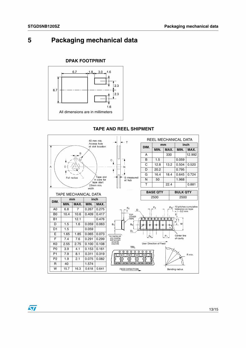
5 Packaging mechanical data
TAPE AND REEL SHIPMENT
DPAK FOOTPRINT
DIM.mm inch
MIN. MAX. MIN. MAX.
A 330 12.992
B 1.5 0.059
C 12.8 13.2 0.504 0.520
D 20.2 0.795
G 16.4 18.4 0.645 0.724
N 50 1.968
T 22.4 0.881
BASE QTY BULK QTY
2500 2500
REEL MECHANICAL DATA
DIM.mm inch
MIN. MAX. MIN. MAX.
A0 6.8 7 0.267 0.275
B0 10.4 10.6 0.409 0.417
B1 12.1 0.476
D 1.5 1.6 0.059 0.063
D1 1.5 0.059
E 1.65 1.85 0.065 0.073
F 7.4 7.6 0.291 0.299
K0 2.55 2.75 0.100 0.108
P0 3.9 4.1 0.153 0.161
P1 7.9 8.1 0.311 0.319
P2 1.9 2.1 0.075 0.082
R 40 1.574
W 15.7 16.3 0.618 0.641
TAPE MECHANICAL DATA
All dimensions are in millimeters

Revision history STGD5NB120SZ
14/15
6 Revision history
Table 9. Document revision history
Date Revision Changes
06-Oct-2003 5 No history because migration
18-Jan-2005 6 Final datasheet
13-Nov-2008 7 Insert new value in Table 2: Absolute maximum ratings

STGD5NB120SZ
15/15
Please Read Carefully:
Information in this document is provided solely in connection with ST products. STMicroelectronics NV and its subsidiaries (“ST”) reserve theright to make changes, corrections, modifications or improvements, to this document, and the products and services described herein at anytime, without notice.
All ST products are sold pursuant to ST’s terms and conditions of sale.
Purchasers are solely responsible for the choice, selection and use of the ST products and services described herein, and ST assumes noliability whatsoever relating to the choice, selection or use of the ST products and services described herein.
No license, express or implied, by estoppel or otherwise, to any intellectual property rights is granted under this document. If any part of thisdocument refers to any third party products or services it shall not be deemed a license grant by ST for the use of such third party productsor services, or any intellectual property contained therein or considered as a warranty covering the use in any manner whatsoever of suchthird party products or services or any intellectual property contained therein.
UNLESS OTHERWISE SET FORTH IN ST’S TERMS AND CONDITIONS OF SALE ST DISCLAIMS ANY EXPRESS OR IMPLIEDWARRANTY WITH RESPECT TO THE USE AND/OR SALE OF ST PRODUCTS INCLUDING WITHOUT LIMITATION IMPLIEDWARRANTIES OF MERCHANTABILITY, FITNESS FOR A PARTICULAR PURPOSE (AND THEIR EQUIVALENTS UNDER THE LAWSOF ANY JURISDICTION), OR INFRINGEMENT OF ANY PATENT, COPYRIGHT OR OTHER INTELLECTUAL PROPERTY RIGHT.
UNLESS EXPRESSLY APPROVED IN WRITING BY AN AUTHORIZED ST REPRESENTATIVE, ST PRODUCTS ARE NOTRECOMMENDED, AUTHORIZED OR WARRANTED FOR USE IN MILITARY, AIR CRAFT, SPACE, LIFE SAVING, OR LIFE SUSTAININGAPPLICATIONS, NOR IN PRODUCTS OR SYSTEMS WHERE FAILURE OR MALFUNCTION MAY RESULT IN PERSONAL INJURY,DEATH, OR SEVERE PROPERTY OR ENVIRONMENTAL DAMAGE. ST PRODUCTS WHICH ARE NOT SPECIFIED AS "AUTOMOTIVEGRADE" MAY ONLY BE USED IN AUTOMOTIVE APPLICATIONS AT USER’S OWN RISK.
Resale of ST products with provisions different from the statements and/or technical features set forth in this document shall immediately voidany warranty granted by ST for the ST product or service described herein and shall not create or extend in any manner whatsoever, anyliability of ST.
ST and the ST logo are trademarks or registered trademarks of ST in various countries.
Information in this document supersedes and replaces all information previously supplied.
The ST logo is a registered trademark of STMicroelectronics. All other names are the property of their respective owners.
© 2008 STMicroelectronics - All rights reserved
STMicroelectronics group of companies
Australia - Belgium - Brazil - Canada - China - Czech Republic - Finland - France - Germany - Hong Kong - India - Israel - Italy - Japan - Malaysia - Malta - Morocco - Singapore - Spain - Sweden - Switzerland - United Kingdom - United States of America
www.st.com