Embed Size (px)
Citation preview
R161 444 NXLLIMETER-WAVE INTEGRATED CIRCUITS(U) ILLINOIS UNJY AT V/2URBANA ELECTROMAGNETIC COMMUNICATION LAB R MITTRAOCT 85 UIEC-B5-8 RRO-18154. 16-EL DRR29-82-K-0084
UNCLASSIFIED F/B 9/5 NL
II EEIIIEIIEIolflnIllllllIIIIIIIIIIII onI//I/I/EEIIIIEEIIIIIIIIIIIIIIIIIIIIIIffIIIf
1 .01 11.5 (*08 ~
IL25 1 .1.
MICR~OCOPY RESOLUTION TEST CHARTMATiONAL buftAu OF STANDARtDS - 1963 -A
*w .17S .

-. N .7 SJ-W W 717- 7.
a SIEtURITY CLASS[IFICATION OF THIS PAGE (Whot Data Entered)ED N RCINREPORT DOCUMENTATION PAGE BEFORE COMPLETING FORM
1REPORT NUMBER 2. GOVT ACCESSION No. 3. RIECIPIENT'S CATALOG NUMBER
I N/A4. TITLE (aid SwbItle) S. TYPE OF REPORT & PERIOD COVERED
MILLIMETER-WAVE INTEGRATED CIRCUITS Final Report
15 Marc~h 1Q9 t-n 7(),S. PERFORMING ORG. REPORT UE
p EC-85-8: UILk NG8-25AR7. AUTHOR(4) 0. CONTRACT OR GRN NUMUER(s)
Raj Mittra DAAG29-82-K-0084
U . PERFORMING ORGANIZATION NAME AND ADDRESS 10. PROGRAM ELEMENT. PROJECT. TASKAREA & WORK UNIT NUMBERSCO Department of Electrical and Computer Engineering
U University of Illinois N/A< 1406 WI. Green Street, Urbana, IL 61801 ______________
II. CONTROLLING OFFICE NAMIE AND ADDRESS 12. REPORT DATE
U. S. Army Research Office October 1985Post Office Box 12211 .NUBROPAE
RpQpnrtrh T 2t1 i( 97 106< 14. MONTOINRAENY WE& AOrES( 1116 iierm, fromt Cotttrolling 01fice) IS. SECURITY CLASS. (of tisl report)
.Unclassified
15a. DECLASSIFICATION/DOWNGRADINGSCHEDULE
16. DISTRIBUTION STATEMENT (el this Report)
Approved for public release; distribution unlimited.
I.DISTRIBUTION STATEMENT (of the abstract attered in Block 20. ii'diffteett 100e, Report)
NA
SO. SUPPLEMENTARY NOTES
The view, opinions, and/or findings contained in this report arethose of the author(s) and should not be construed as an officialDepartment of the Army position, policy, or decision, unless so
19. EY ORDS(Cmtinu onreverse side It neccessay and Identify by block ntmer)
microwave transmission linesmodal characteristicsdiscontinuities in transmission lines
* microstrip thin linesS20. 1A~rUACr (9M10 dw Powwown &Nt noeweumy and Identify by block numbee)
,;- In this report, a number of topics are considered that concern printedScircuits and printed circuit discontinuities. First, propagating and evanescentmuodes of a shielded microstrip are calculated using the spectral Galerkin tech-nique. The characteristic impedance and field configurations of these modes are
L~j also calculated. These modes are then used in a mode matching technique, in order_J to calculate the scattering from abrupt discontinuities in the microstrip.
1j Results are given for various configurations of single and cascaded discontin-uities. Next, the singular integral equation technique is used as an alternative
W JM,0' 1C3 90#lON Of I NOV5 4S 06CLETE (NLSIIDover)
UNCLASSIFIED..........................................C=...........................................o.............
25. .. . ...6
SC9CUMIIY CLASSIFICATION4 OF THIS PAOK(W1 DOW& ftgharod)
to the spectral Galerkin technique, to calculate modes in a shielded microstrip. '
These results are compared to those generated by the spectral Galerkin technique.Finally, the coupling between multiple transmission lines is considered, byusing the coupled-mode theory. Results for the propagation constants of thevarious modes of propagation, as w~ell as for the transfer of current from oneline to the next, are presented.
UNCLASSIFIED
SECURITY CLASS1r'CA-'n-j ')9 1TIS PAGEfWhon, Doets Fn!r-'.
" ,4 4d / e2 t, . /t,- t
UILU-ENG-85-2568
ELECTROMAGNETIC COMMUNICATION LABORATORY REPORT NO. 85-8
MILLIMETER-WAVE INTEGRATED CIRCUITS
Final Report
U. S. Army Research OfficeDAAG29--82-K-0084
NTIS c-ny
D71C T, .
I IT% ~ I ~
-
~Av-ai i : ! ! -C c e s -- -
Raj Mittra
University of Illinois -i
at Urbana-Champaign
3
October 1985
Approved for Public ReleaseDistribution Unlimited
85 11 18 256
.::%
V
TABLE OF CONTENTS
Chapter Page
1. INTRODUCTION ................................................................................... 1
2. UNIFORM NIICROSTRIP ANALYSIS .......................................................... 32.1 Introduction ................................................................................ 32.2 The Spectral Domain Immitance Approach .............................................. 32.3 The Spectral Galerkin Technique.........................................................1I12.4 Basis Functions ............................................................................. 132.5 Characteristic Impedance................................................................... 162.6 Fin Line Calculations....................................................................... 202.7 Field Configurations ........................................................................ 242.8 Results for Uniform Microstrip and Fin Line........................................... 242.9 Conclusion.................................................................................... 36
3. DISCONTINUITY CALCULATIONS .......................................................... 373.1 Introduction .................................................................................. 373.2 Mlode Matching ............................................................................. 383.3 Orthogonality of Inner Products ............. I............................................. 433.4 Condition Number of the Mlatrix.......................................................... 443.5 Mlatrix Theory for Cascaded D~iscontinuities ............................................ 443.0 Results Ifor the Single Discontinuity...................................................... 493.7 Results for Other Discontinuities.......................................................... 533.8 Conclusion.................................................................................... 57
4. THE SINGULAR INTEGRAL EQUATION TECHNIQUE................................... 624.1 Introduction................................................................................ 624.2 Overview of the Mlethod ................................................................... 624.3 Calculations of P,,,. K,. and ............................. .............................. 704.4 Results ........................................................................................ 744.5 Conclusion.................................................................................... 75
5. COUPLED-MODE ANALYSIS OF MULTICONDUCTOR, MICROSTRIP LINES .... 765.1 Introduction .................................................................................. 765.2 Calculation of %lodes .................. .................................................... 785.3 Coupled-mode Theory .................... ................................................. 805.4 Results ........................................................................................ 815.5 Conclusion.................................................................................... 83
6. SUMMARIES OF OTHER ACTIVITIES AND IMPORTANT RESULTS................ 88
LIST OF PUBLICATIONS AND TECHNICAL REPORTS........................................ 90
SCIENTIFIC PERSONNEL AND DEGREES AWARDED......................................... 93
REEENE ...................................................................... 9
-.. . . .. . . . . .. . -... . .
. . . . . . . . . . . . . . . . . .. .
vii
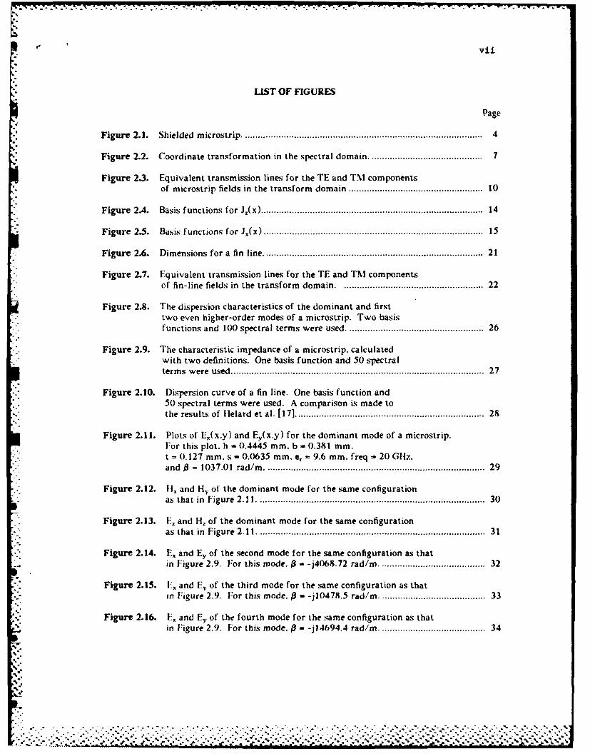
LIST OF FIGURES
Page
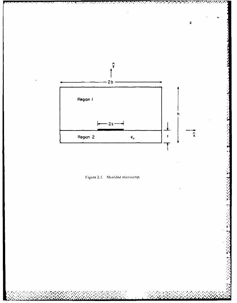
Figure 2.1. Shielded m icrostrip ............................................................................................. 4
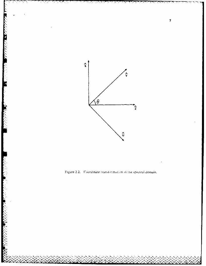
Figure 2.2. Coordinate transformation in the spectral domain ........................................... 7
Figure 2.3. Equivalent transmission lines for the TE and TM componentsof microstrip fields in the transform domain ................................................. 10
Figure 2.4. Basis functions for J,(x) ................................................................................... 14
Figure 2.5. Basis functions for Jx(x) ................................................................................... 15
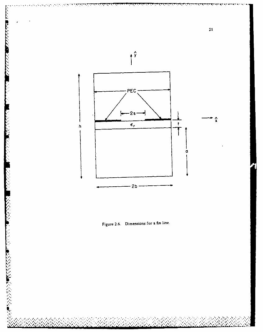
Figure 2.6. Dimensions for a fin line ................................................................................... 21
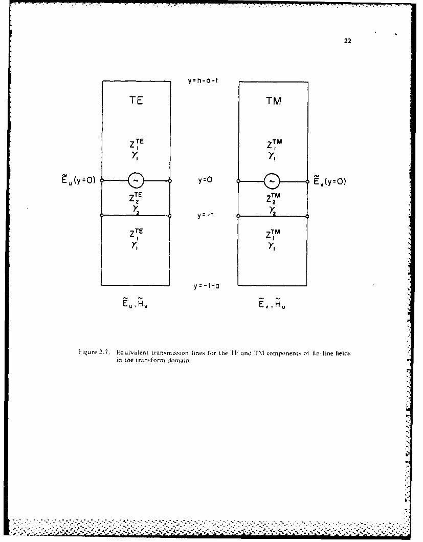
Figure 2.7. Equivalent transmission lines for the TE and TNI componentsof fin-line fields in the transform domain ................................................... 22
Figure 2.8. The dispersion characteristics of the dominant and firsttwo even higher-order modes of a microstrip. Two basisfunctions and 100 spectral terms were used ................................................... 26
Figure 2.9. The characteristic impedance of a microstrip, calculatedwith two definitions. One basis function and 50 spectralterm s w ere used ................................................................................................ 27
Figure 2.10. Dispersion curve of a fin line. One basis function and50 spectral terms were used. A comparison is made tothe results of Helard et al. [17] ...................................................................... 28
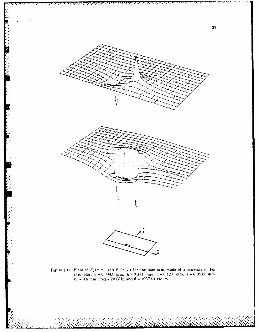
Figure 2.11. Plots of E,(xy) and Ey(x.y) for the dominant mode of a microstrip.For this plot. h = 0.4445 mm. b - 0.381 mm.t = 0.127 mm. s = 0.0635 mm. e, - 9.6 mm. freq - 20 GHz,and B = 1037.01 rad/m .................................................................................. 29
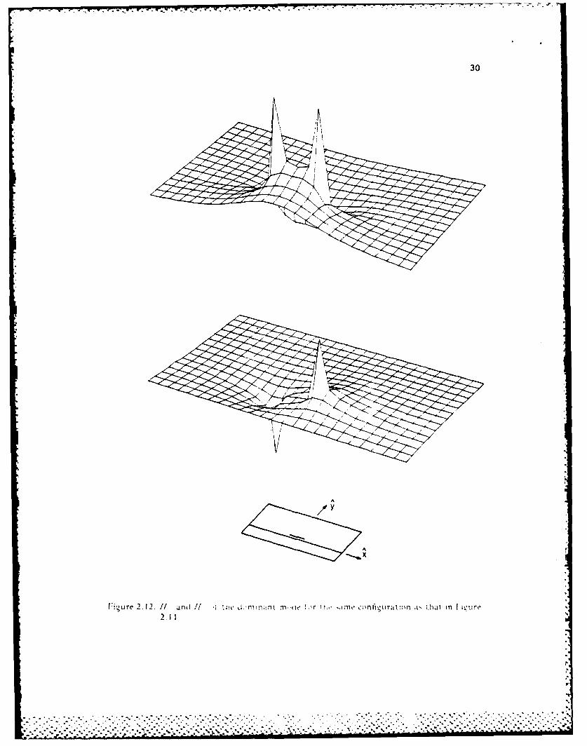
Figure 2.12. ll, and H. of the dominant mode for the same configurationas that in Figure 2.11 ...................................................................................... 30
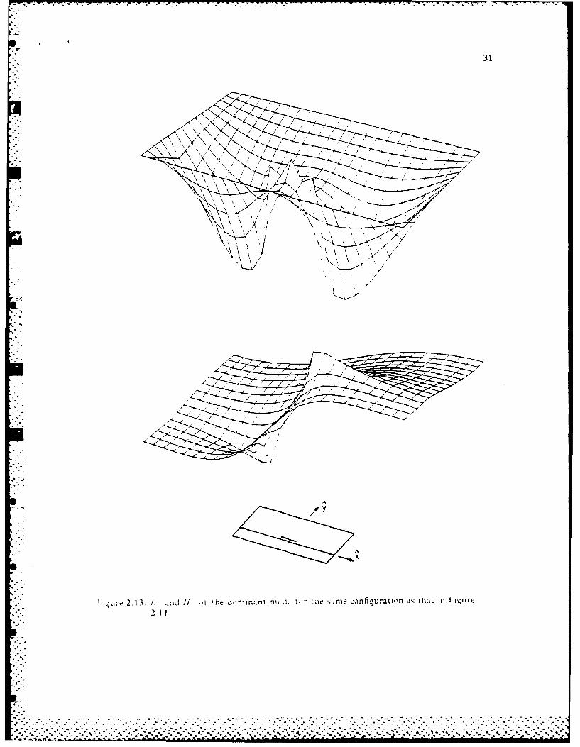
Figure 2.13. Ez and H, of the dominant mode for the same configurationas that in Figure 2.11 ...................................................................................... 31
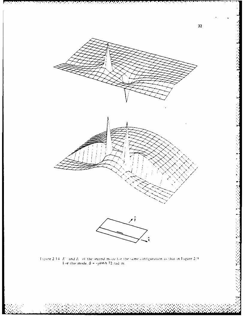
Figure 2.14. E, and Ey of the second mode for the same configuration as thatin Figure 2.9. For this mode. 3 - -j4068.72 rad/m ...................................... 32
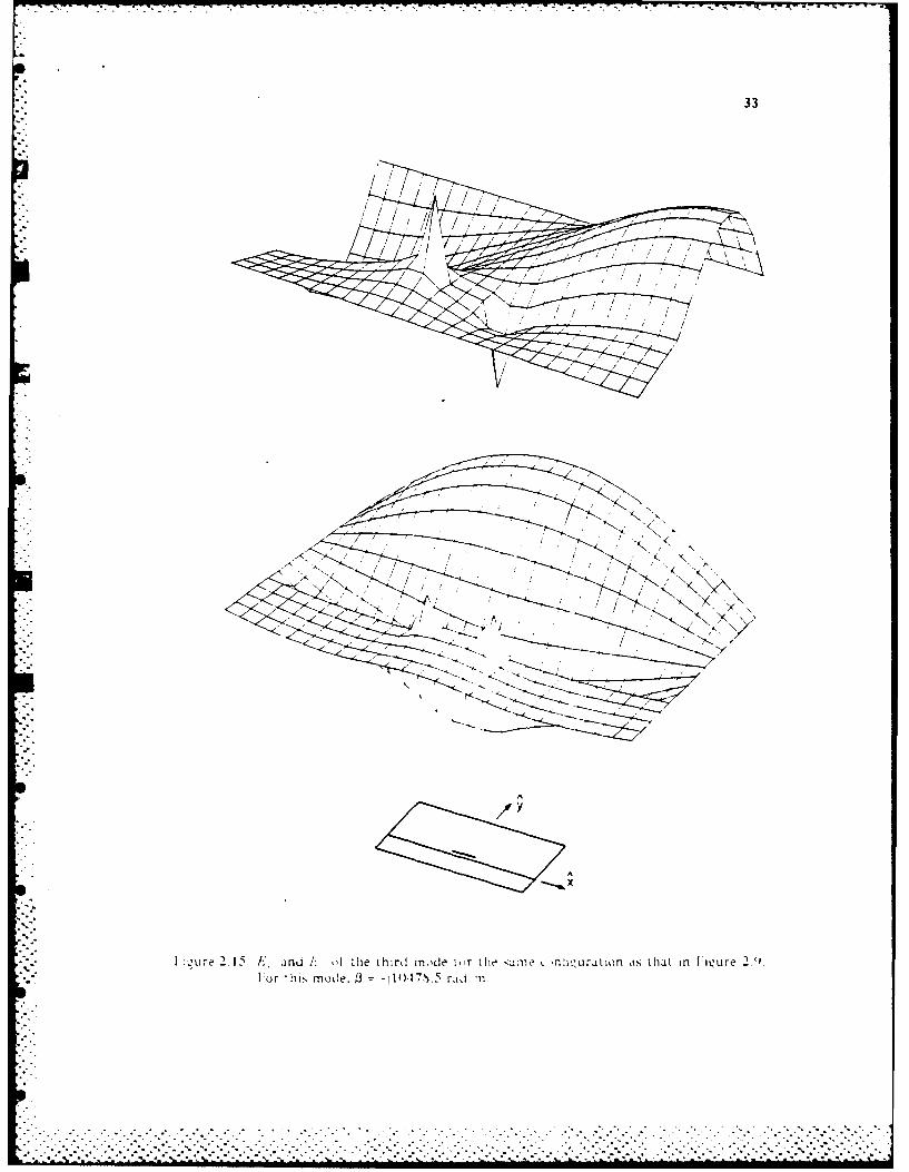
Figure 2.15. Ex and F, of the third mode for the same configuration as thatin Figure 2.9. For this mode. = -j10478.5 rad/m ...................................... 33
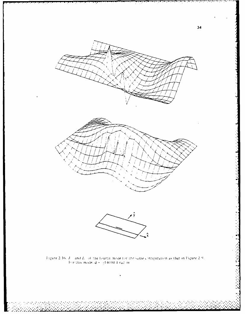
Figure 2.16. F-.2 and E, of the fourth mode for the same configuration as thatin Figure 2.9. For this mode. P = -j14694.4 rad/m. ..................... 34
.i.
. .-- .- .--. .. ... .... . . . . . . . ..-. .. . .. . ..- ..... . ...... .... - ,- -..... .. .-.S. .-.... ......-.-...--.. ....-..-.-.. .. .
viii
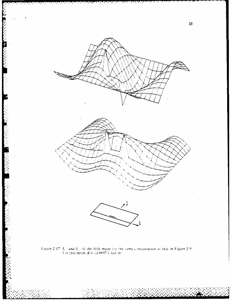
Figure 2.17. E, and Ey of the fifth mode for the same configuration as that
in Figure 2.9. For this mode.0 = -j14897.1 rad/m ...................................... 35
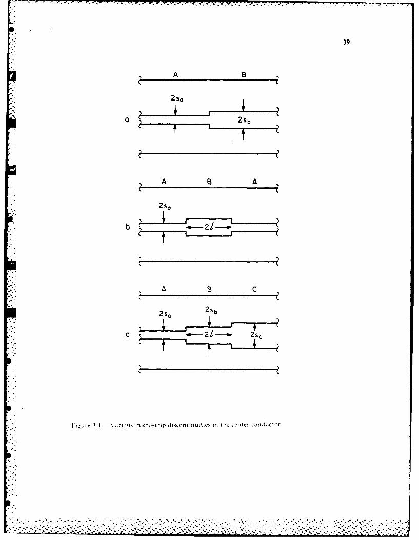
Figure 3.1. Various microstrip discontinuities in the center conductor ............................ 39
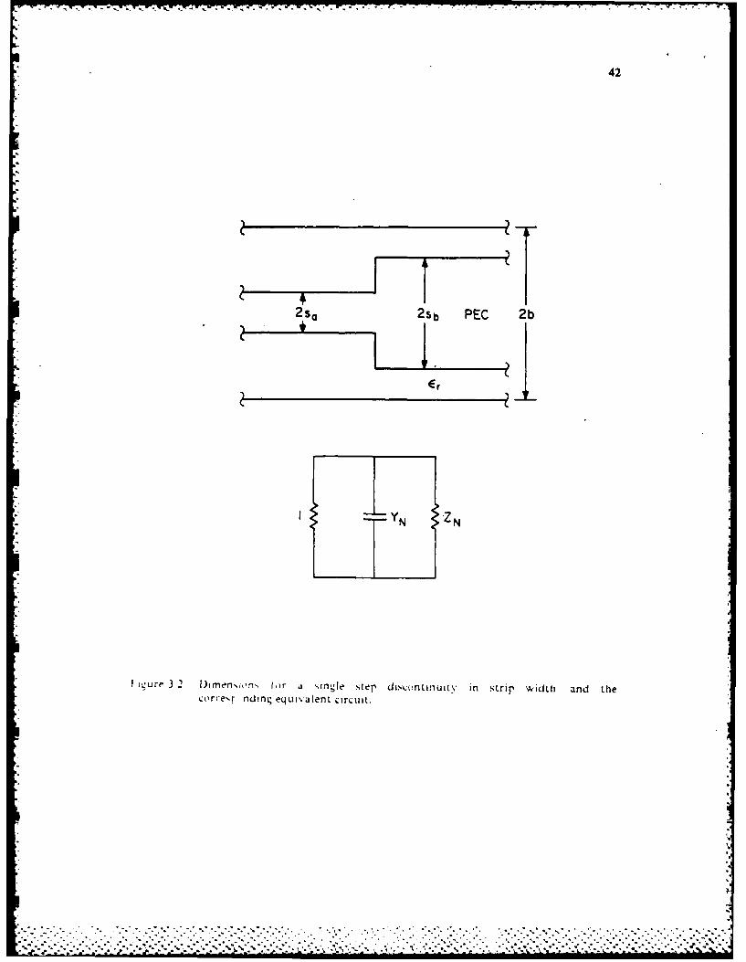
Figure 3.2. Dimensions for a single-step discontinuity in strip widthand the corresponding equivalent circuit . ..................................................... 42
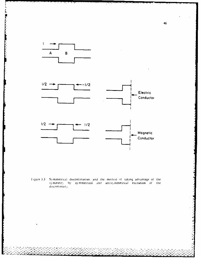
Figure 3.3. Symmetrical discontinuities. and the method of takingadvantage of the symmetry by symmetrical andantisymmetrical excitation of the discontinuity ........................................... 46
Figure 3.4. Input and output parameters of an arbitrary circuit,and a cascade of such circuits ........................................................................... 47
Figure 3.5. Dimensions for a symmetrical double step discontinuity instrip w id th ......................................................................................................... 54
Figure 3.6. Dimensions for a model of a microstrip taper. modeledas a cascade of discrete discontinuities . ........................................................ 58
Figure 3.7. )imensions for a step discontinuity in dielectricconstant. strip width. and substrate thickness ............................................... 60
Figure 4.1. LDimensions of a shielded microstrip for this chapter .................................... 63
Figure 5.1. Configuration of microstrip with five lines. For these calculations.t=2sf= I mm .2s,=0.2 mm. and er=i O ........................................................ 77
Figure 5.2. Dispersion curves for the first five modes of propagationof amicrostrip with five lines. The dimensions are the same as thosein F igu re 5 .1 .............................................. . ........................................... ... 82
Figure 5.3. J,(x) for the first even m ode ............................................................................ 84
Figure 5.4. J,(x) for the second even m ode ........................................................................ 84
Figure 5.5. J,(x) for the third even m ode .......................................................................... 85
Figure 5.6. J,(x) for the first odd m ode .............................................................................. 85
Figure 5.7. J,(x) for the second odd mode .......................................................................... 86
Figure 5.8. Variation of I with z at 1 GHz for each of the five strips ............................... 87
Figure 5.9. Variation of I with z at 10 GIlz for each of the five strips ............................ 87
". . . . . .. . . .- - ' ',.. . .... ".,.. . .- ".,. .-.. .
CHAPTER 1
INTRODUCTION
The primary objective of this effort has been the investigation of dominant and
higher-order model characteristics of microstrip lines and fin lines that find application in
millimeter-wave integrated circuits. The investigation of higher-order modes is important
for the analysis of discontinuity problems in planar transmission lines: these problems have
been the focus of attention in this project during the entire grant period. The study of the
discontinuity problems is of interest from the point of view of designing practical
components, e.g.. filters, impedance matching networks, and transitions between rectangular
waveguides and planar transmission lines. The higher-order modes have been analyzed
using the spectral domain technique introduced by Itoh and Mittra [1. 2]. The propagation
constant. characteristic impedance and field configuration are obtained for the dominant and
higher-order modes in planar lines. The model characteristics are then employed to analyze
some typical discontinuities in planar lines using the mode-matching procedure [3. 41.
which has been extensively employed in the past for the solution of similar problems in
other types of waveguides. Ilowever. the situation with regard to the application of the
mode-matching procedure is found to be quite different for the case of planar waveguides
when compared to that of rectangular guides because accurate generation of higher-order
model fields becomes a formidable problem in planar guides. whereas this task is quite
straightforward for rectangular guides. Thus. it becomes important to investigate
effectiveness of the mode-matching procedure when only a relatively small number of
" modes are available and the higher-order modes are known only approximately.
-- _ In an attempt to enhance the accuracy of the higher-order mode computation. the
singular integral equation technique is used. This technique was originally employed by
Mittra and Itoh [5] for the analysis of planar transmission lines. This technique is further
developed in this work and the results obtained via the application of the singular integral
% %%
2
equation technique are compared with those derived from the spectral domain approach.
Another interesting problem in planar transmission lines, viz.. the coupled multiconductor
lines is analyzed in this work using the spectral domain approach.
To the best of our knowledge a full-wave coupled line analysis of n planar
transmission lines has not appeared elsewhere in the literature.
....................
......................-
o... ~ .. . . .
. . . . . . . . . . . .,. - . . . - ...
3
CHAPTER 2
UNIFORIM NMICROSTRIP ANALYSIS
2.1 Introduction
The analysis of various printed circuits has been of interest for a number of years.
We find it of interest here. because the first step of the mode matching procedure is to
generate the dominant and higher-order modes in a uniform microstrip. A cross section of a
shielded microstrip is shown in Figure 2.1. This and related structures have been analyzed
by a number of workers using a variety of techniques. These techniques include various
quasi-static methods [6-91. nonuniform discretization of integral equations [10]. a modified
Weiner-Hopf technique [11]. a singular integral equation 'technique [5]. and the spectral
Galerkin technique [1.2.12-171. The method that is simplest to implement while giving
excellent results is the spectral Galerkin technique. This is the method considered in this
chapter.
In order to allow mode matching work to a high degree of accuracy. it is necessary
to calculate as many evanescent modes as possible. The feasibility of generating a large
number of higher-order modes imposes the largest constraint upon the accuracy of the
mode matching solutions. To date. there is little information available on evanescent modes
in a shielded microstrip. although the propagating modes have been well studied.
In this chapter, we present data on the dominant and first few evanescent modes of
a microstrip. showing dispersion curves, characteristic impedance calculations, and field
distrbutions. Let us proceed now with the analysis of a uniform microstrip.
2.2 The Spectral Domain Immitance Approach
In order to find information about waveguide modes, the quantity of most
immediate interest is the propagation constant. 0. To find 0. a matrix equation must be
found of the form
o-
bb.
4
Ay
,, 2b .
Region I I'.
Region 2 Er t
ligure 2.1. Shielded microstrip.
ix
%%
S.
.- .-.-....-.........-......--.-.--... '. ...... ....... ...........'...........-. ..... ''' '.. ... ..-..- ".....-..-..-..-.... .-. .....
'. . . . ... ..... ...,,. -.,, ., ,,,. ., , ., * . ,., .,,,, . ,.. ,,* * .,...... . -* .'.., . '.S, .,,.,-,-,.,...,,,.,...,
5
Z h (2.1)i i,(11 .L 1i.(
where J and E are the Fourier transforms of the current and electric field in the plane z-O.
and the Z's form the components of a dyadic Green's function. In order to find this Green's
function, we use the spectral domain immitance approach. This approach is a method of
generating the dyadic Green's function in a straightforward manner, that will be useful for
many different kinds of printed circuits, including microstrip. fin line. and coplanar
waveguides. The work in this section follows Itoh [131.
We begin by setting up a scalar Helmholz equation in each of the regions 1 and 2. as
shown in Figure 1. Assuming an e ( - z dependence. we obtain
Oi (x .y)(V 2 +Ek o2 ) = 0 (2.2a)
.'°.
where
'E e Region 1 (2.2b)Region 2
As the equations now stand. the TE. and TMY fields are coupled. In order to decouple these
equations we must work in the Fourier transform domain. Thus. for example.
0(n.y)= f O(x.y)e 'dx (2.3a)
(x .y ) (n y (2.3b)
=(n -%)v (2.3c)b
The above choice of ck, is suitable for modes that are even in J1, such as the dominant
mode. This choice enforces the boundary conditions at x = ±b. For modes that are odd in
....
* .. ** . . . . . . ...
J.we choose a,,= n rib. In the transform domain. the Helmholtz equations become
2 + 2 +e, k02) (n -' (2.4)
or
S(n). =0 (2.5)
ay 2 ki(n)
where
= o,2 + 02- -, ko2 (2.6)
Thus. in the transform domain we can reduce the problem to two tramsmission line
equations.
Let us now introduce the transformations
:= NZ -N v(2.7)
where
N - __ - sin (2.8a).. ar2 + 02
N, + Coso (2.8b)
This transformation is shown is Figure 2.2. With this transformation. we see that all scalar
potentials and fields are of the form
((n v e = f (x.y)e + 1 (2.9)
The transformed equations are dependent only upon v; hence - 0 = . This decouples
v7
AA
AF
-. Figure 2.2. ('Nordinate tran~l, rnLiun in tue spe-ctraI domain.
.............................................
o. . -
o U ' . . - -- ~:-- - - " . . - .- * .*~*o p*. V % % - ~ ~ .% ~
8
Equation 2.5 into TEy components (Ji,. i.. and ii,) and TMy components (6y E4v. and
H'a ). We now show how this separation takes place. and that the TE, components are due
to Jl . and the TMy components are due to IF.
Let us derive the expressions for the field components. To begin, we express the
vector potentials as
Ti fi ) i (X -y) (2.10Oa)
Ai = 27 , (xy )(2.10b)
Adapting some results from Harrington [181 on the separation of TE and TM fields, and
using the fact that = ', and 0 O. we obtain the TE components
SE, -0 (2.11 a)
(2.11b)
'_ v, ' , (2.11c)j, W1,8
H, =.( + k,2) (2.1 ld)
-. =0 (2.1 le)
and the TM components
-Y, ^0 (2.12a)
Sy + k,2) (2.12b)
= 0 (2.12c)
Ip
* . . .-' " , " "'. . . °• ", "• - ".% •. .. •. . % -. . % ". '."• o •. •a . "."• .". , "°". % %.". . ". %°%" .' '. -." . .g " "• .4.-
9
H~=H 0 (2.12d)
=- (2.12e)
From these equations, we can set up equivalent transmission lines for the TE and TMI cases.
The characteristic impedance of each line is
Z TE, = - = (2.13a)
ZrVI= (2.13b)
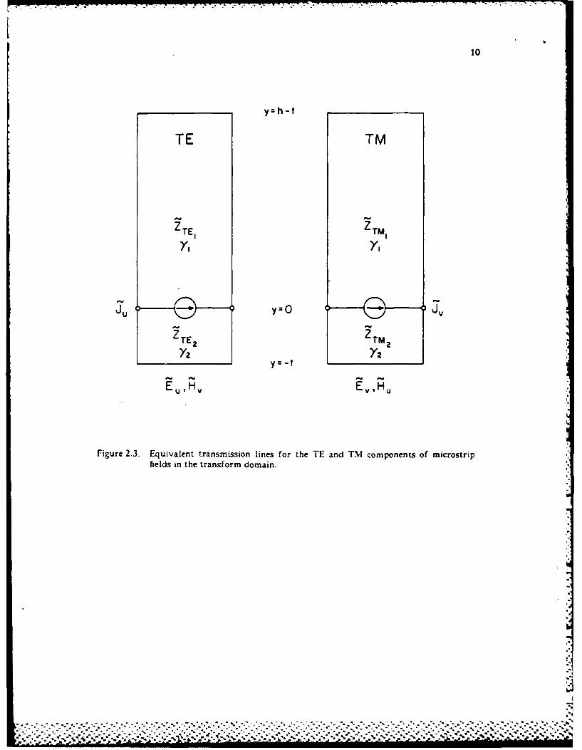
The propagation constant for each line is and the sources for the lines are J,. for the TE
line and i. for the TM line. These equivalent lines are shown is Figure 2.3. From the
input impedance of the shorted line sections. we obtain the input impedance at z =0 as
+ ______(2.14a)
ZrMWtanh y1I(h -tY ZTA 2 tanh y2t
1h + I(2.14b)ZrE~tanh Y,(K-t ZrE2 tanh V21t
* Given this input impedance. we may now write
E(n y=0) =VJ(n y =0) (2.15a)
E(n y =0)Z J~(n y=0) (2.15b)
Furthermore, we can transform these equations back into x and z coordinates using
* . Equations 2.7 and 2.8 to obtain
- - .. (2.16)
P.."
10
TE TM
ZTEI ZTMI
U V
Z TE 2 ZTM2
Y2 ~ y Y-t Y
Figure 2.3. Equivalent transmission lines for the TE and TMI components of microstripfields in the transform domain.
....... ~.. ... .... ... .... ...
i~~i - : -. . . . , .- : . . J: ... .. .. ... . .. . .. .- - .. . . . . . . . . . . . ,-
o. 11
where
ziz N. 2ze + N,2iZ (2.17a)
Z,, =Z = N, N, -i' +i h ) (2.17b)
i = Nx2Zi + NZiZ (2.1 7c)
This is the equation that must be solved to find 0. Once is found. all other quantities of
interest, such as field configurations and characteristic impedance. may be found.
It is helpful at this point to briefly discuss the applicability of the spectral domain
immitance approach to structures related to the microstrip. Since the equations are
separable in the transform domain, we see that if we have multiple layers of dielectric, this
will be equivalent to having extra sections in the transmission line model. Furthermore.
multiple strips can be represented as extra current sources, and slots can be represented by
voltage sources. Therefore, we can use this method of generating the dyadic Green's
function for a large class of planar waveguide structures. These include fin line. coplanar
waveguide. and slot line. The generality in this procedure for generating the Green function
maintains the generality of the mode matching procedure,
2.3 The Spectral Galerkin Technique
Now that we have found Equation 2.16, we must solve it for with the spectral
Galerkin technique. The work in this section follows Schmidt and Itob [15].
We proceed by expanding the currents on the strip as a sum of basis functions
N
I.(x) = (x) (2.18a)._ i=1
... ., (X ) d , 71 (x ) (2.18b)
These basis functions are now Fourier transformed according to Equation 2.3 and
-UU.
,-
~~~~~~~~~.. .... ri ...............- i -i -- --
12
substituted into Equation 2.16. By taking the inner product of the resulting equation with
S(x) and 71i (x ). we can eliminate the E-fields in this equation. This is true because f, (x)
and i,(x ) are non-zero only where E, and E, are constrained to be zero, since they are
tangential to the strip. Since this is true in the space domain. Parseval's theorem [18]
guarantees that it will also be true in the spectral domain. Hence, we obtain the equations
Al1 NKfc, + Kgxd, =0 p =1.. (2.19a)
,%z ,+ Kgj ,=0 q1=I...N (2.19b)
where
= z 4(n)Z, (n0) ,(n) (2.20a)
K,1z 74~i~(n)Zxz(n.03) ,(n) (2.20c)
Kq'7 = 71 (nl Z~ (nl 1 l, (nl (2.20d)
A solution to this equation exists if and only if the determinant of the coefficient matrix is
equal to zero. Thus.
Kz Kz_
where, for example. K is the matrix of coefficients given in Equation 2.20a. We may now
find the zeros of f(13) with a zero-finding algorithm such as Newton's method, thus
completing the solution for .
13
2.4 Basis Functions
One of the most important aspects of the spectral Galerkin procedure involves the
choice of basis functions. A good set of basis functions can greatly increase the efficiency of
the solution. as well as its accuracy.
The basis functions should satisfy three conditions. First. -hey must be
analytically Fourier transformable, since they are used in the transform domain in
Equation 2.16. Second. they should have a shape that is similar to that for the current we
expect to find on the strip. Having this property will reduce the size of the matrix
equation. Finally. they should have the properties that J, (x) hat a 1/"x singularity at
the strip edges and that 1, (x) is zero at the strip edges. This is the result expected for the
current parallel and perpendicular to a knife edge. By not satisfying this last condition,
more basis functions will be required to represent the currents, resulting again in an
increased matrix size.
One appropriate choice of basis functions for modes that are even in J, (x) is
suggested in [15] as
c Cosf(i-l) '(x/s + 1) (2.22a)1 - (xis )2
sin [ir (x Is + 1)] (2.22b)
-,/I - (x Is )2
These functions satisfy all the above criteria. In particular. note that , (x) has a /x
singularity at x =- s and that )i (x=±s) 0. which can be shown by I'Hopital's rule.
The first few functions are shown in Figures 2.4 and 2.5. The Fourier transforms of these
functions are
(-)'-sir [J(Ct s + (i-l)r) +J,(a,s -(i-1)7r)] (2.23a)2
.. "i (n) -) [J, (0" s + V o) - J,, (0, S -W o)] (2.23b)2)
'... ..........................................9, '**.** * ** * **•
* * * %* . *
14
3
2%
E"T
-2 i I
X/S\ ,7
11.0
Figure 2.4. Basis functions for 1. (x
....................-...
X/'
- . ::.-:--:~~:<. *Figur'2..* '*asis functions for .*'*- (.*

*1 15
223 -
-1. .*S 0.0 O.S 1.0
X/s
Figure 2.5. Basis functionS for J. (x)
16
where j = v and 1o (x) is the zeroth order Bessel function. A formula that is useful in
deriving the above transforms comes from the Bateman Manuscripts [191. Hence.
T• (x1)e dx = (-1) i n rJ (y) (2.24)
where T, (x) is the nth order Chebychev polynomial in the interval I x I < I and zero
elsewhere, and T. (x) = 1.
2.5 Characteristic Impedance
The characteristic impedance of a microstrip is a useful parameter to calculate for
several reasons. It serves not only as a useful design tool. but also as a check on the
accuracy of the dominant mode propagation constant. In addition, the inner product we use
in the mode matching procedure uses an inner product that is very similar to characteristic
impedance. Hence, it will be useful to compare our calculated values of characteristic
impedance to previous calculations [11.12].
At this point, mention should be made of the ambiguity inherent in this
characteristic impedance calculation. The characteristic impedance of a transmission line is
usually thought to be a characteristic of TEM transmission lines. The dominant mode of
the microstrip is only quasi-TEM. however, so there are several definitions of characteristic
impedance in this case that make sense and yield similar, but unequal results. A number of
authors have discussed the relative merits of the various definitions [20-23]. These
definitions include
Z= " (2.25)
1-S"7" (2.26)
and
.
c.'
. ,.t .. .a" 'm."b , d i .... ...... ~ i i . ....
* .. -P
17
zo W. (2.27)_2P
where
h b
P =A Re f f E x i dx dy (2.28)
I f 1(x) dx (2.29)-$
0
V - f E, (x =0.y) dy (2.30)
These are the so-called power-current. voltage-current, and power-voltage definitions. It
turns out that the definition most widely accepted is the power-current definition, and that
is what we calculate here. For comparison, we also calculate the characteristic impedance
with the voltage-current definition. Thus. we need to calculate P. I. and V.
First, let us calculate I and V. Proceeding from Equations 2.29 and 2.30. it is
straightforward to show that
NI = c, ,(n =0) (2.31)
i=1
fV - f (n.y )dy (2.32)
Next. we proceed to the power calculation. Beginning with Equation 2.28. and
subsequently using Parseval's theorem [24]. we obtain
P (n) (2.33)
b4where
f (n) f (4, W -i, :) dy (2.34)
--
,.... ° .o.. .. ,..' . •° °°. o .......... °.....°° °b.. °%.. °°......°.. °. °...... °°""°.
........ .........
The task now becomes one of finding expressions for the field components in the transform
domain. In order to find these, we first need to solve the transmission line problem shown
previously in Figure 2.3. The solution is straightforward. and can be adapted from a
number of standard textbooks, for example. Mayes [251. This results in the following set
of equations
H1 (n y A (n) XC(y) (2.35a)
Em (n .y) = -ArE(n ) XoS(y) (2.35b)
H (n .y) = A1r' (n ) XS(y) (2.35c)
E,, (n .y ) - A ,rT(n ) XC(y) (2.35d)
where
cosh yl(Y - (h -t))
sinh V1j(h -t) =1Xc = (2. 36a)= cosh ) 2(y +t) 2 =32
sinh y2t
sinh "yl(y - (h - £
sinh, 1 (h -t) = IXs= (2.36b)
sinh y2(y + t) =2
sinh 72t
and
A4"E -Z sinh y((h -t2V Z - sinhy.-t
(2.3 7 a)
A . -Z sinh -y1(h - )- = Z ___.___s __nh _ _ (2.37b)
4 ~~ r%1Z~sinh yy
.. ....... -. - . ...- . -.- ... -.. -.-.... . - .. . . . -,.-. - .o °°-%'°,•... -. °% . = .
19
AV = -h(n) 23c
coth - 1(h - t ) - - coth y -t
J1 , (n)= [ A r' (2.37d)
cothY 1(h -t)- AFT cothyt(
1 Af
The signs of the current terms in the above equations are determined by the boundary
condition [26]
X x(TI I- T 2) =7, (2.38)
where H I and H 2 are the H-fields just above and below the strip. In the spectral domain
this condition is
."-H /- , -1 , =., (2.39a)
H 1, H 2 , =-J, (2.39b)
This completes the derivation of the fields in the decoupled u.v coordinates.
In order to express the fields in x.y.z coordinates, we need to invoke the coordinate
transformation given previously in Equation 2.7 and then combine the TE and TM parts of
the fields. This results in the following set of equations:
E,(n: y N2 AfEZT + N, A!"' TM X (2.40a)
E,, (n .y) -=f Ar XF (2.40b)
E., (n .y ) = -N, AZTEZrT + N, A!"Z1TMj X8 (2.40c)
Jif n .y) = N. A,Tr -N. Af'!J' Xf (2 .40d)
fe° -' I- P
20
- A z,rIT , X (2.40e)
H[,(n.y ) = N, AITE + N A,r Xf (2.40f)
The y dependence is contained in X c and X s . These fields can now be substituted into
Equation 2.7 to calculate f(n). In order to carry out the integration of f(n). we need only
integrate over the products of hyperbolic cosines and sines, which can be carried out
analytically. This concludes the power calculations and. hence, the characteristic
impedance calculation.
2.6 Fin Line Calculations
Although it is very easy to verify the dominant mode microstrip calculations. very
little data exist for the evanescent modes. We would, however, like to have a comparison
for our calculated evanescent modes. It turns out that fin line evanescent modes have been
calculated. In order to verify our evanescent modes, therefore, the best we can do is to
alter our program to calculate fin line evanescent modes, and compare these to those in the
literature [17]. A diagram of fin line is shown in Figure 2.6.
In order to adapt the spectral domain immitance approach to the fin line. we need to
,e a different matrix equation. This is of the form
Y 7 Y = E, j (2.41)
where E, and E. in the fin line are analogous to J, and J, in the microstrip. respectively.
In order to find the admittances. we must set up transmission lines analogous to those in
Figure 2.3. These are shown in Figure 2.7. From these transmission lines we obtain the
dyadic admittance matrix
SN,2 Y' + N.2 Y Y (2.42a)
%%
"l o . . . " o . q 1. . -. . . . . . . . . . . . . . . . .
PEC
SA
her -t
Figure 2.6. Dimensions for a fin line.
22
yzh-o-t
TE TM
TE TM
E (y =0) ' jyiO - ECY=O)TE TMz 2 z2
y=-t Y
TEZ1M
y:--
F~igure 2-7. Equivalent transmission lines I'r the IT and 'B! components of fin-line fieldsin the transform domain.
23
Y2 X =., = N, N, 1 -17" +1 7J (2.42b)
i,, = N 2 j" + N 2 Y (2.42c)
where
-, 1= Z Te' tanh y 1 (h -a -t)
1 + Z tanh yla tanh ,t+ =Z Zj ' tanh -ya + Z rM tanh ( at
ZrE tanh -- )
S1 Zr +Z7 tanh2 1 ya tanh ,2t+- Z rE tanh y , + Z rE tanh (2.43b)
The matrix equation is now solved in a manner very similar to the microstrip matrix
equation. We expand E, and E. in the same basis functions used previously for 1, and
J, .respectively. These basis functions were given in Equation 2.22.
Finally. we must reconsider the definition of the Fourier transform before we solve
the fin line problem. In the transform used previously in Equation 2.3. we used
", = (n - 1/) r/rb. This value of a,. however, is no longer valid for the even tin E,)
modes of the fin line we are calculating, which include the dominant mode. The correct
choice is now , = n 7r/b. This choice enforces the boundary conditions of the zero
tangential E -field and normal H -field at 1x1 = b. If we were interested in the odd modes of
the fin line, the first definition of a, . = (n - Vz)w/b would be correct.
S. In general. we pick i,, f n 7r/b when (x) is even and k(x) is odd. where x) and
-t(x) were defined previously in Equation 2.2. This occurs for even (in J,) microstrip
modes and in odd (in E,.) fin line modes. Furthermore, we pick a, = (n - V)r/b when
W(x) is odd in Vo(x) is even. This occurs in odd (in .4) microstrip modes and in even (in
E, ) fin line modes.
% %""-., . .. .. • :.... • v ..,.'..........."...'..':....°...,..........,.................,..... ..... y:..... ....................... :
• ,.. ._...F " "" "... ".......... "........ "..... "...."
24
2.7 Field Configurations
It is of great interest to plot the fields due to the dominant and higher-order modes
over the cross section of the waveguide. This provides verification that the boundary
conditions have been satisfied and offers physical insight into the structure of the modes.
The field configurations may be obtained from the transformed fields obtained in the
characteristic impedance calculation, by performing the inverse Fourier transform of
Equations 2.35. Results are presented in the next section.
2.8 Results for Uniform Microstrip and Fin Line
In this section we present numerical results for the techniques discussed previously
in this chapter. The first item we consider is the convergence of the dominant mode
propagation constant with respect to the number of basis functions and number of spectral
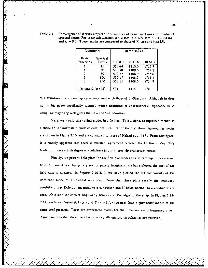
terms used. In Table 2.1 we show these calculations and compare our results to those of
Mittra and Itoh [5]. From this table we can make a number of observations. First, our
values of 03 are in very good agreement with those of Mittra and Itoh. Second. our values
of 0 have converged sufficiently with two basis functions and 50 spectral terms. Note that
"2 basis functions indicates two functions for J, and two for J, . Note furthermore that
50 spectral terms indicates that all series were summed from n - -49 to 50.
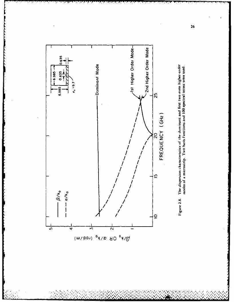
Next, we present a sample dispersion curve for a shielded microstrip. This is shown
in Figure 2.8. Note that the dominant mode is not cut off. while the first higher-order mode
is cut off below about 20 GHz.
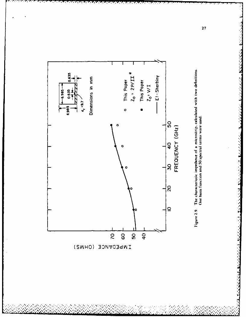
Next, we present data on the characteristic impedance of a shielded microstrip. This
is shown in Figure 2.9. The impedance has been calculated using both the V-I and the V-I
definitions, as discussed in Section 2.5. and the results are compared to those of El-Sherbiny
[11]. Note that in EI-Sherbiny's paper. the impedance was calculated for a shielded
microstrip without side walls. In order to account for this. we chose in our calculations to
move the side walls far enough from the strip to eliminate their effect. Our results for the
.. " . . ... . .
25
Table 2.1 Convergence of j with respect to the number of basis functions and number ofspectral terms. For these calculations. h - 2 mm. b - 1.75 mm. t - s - 0.5 mrm.and e, - 9.0. These results are compared to those of Mittra and Itoh [5].
Number of O(rad/m) at
Basis SpectralFunctions Terms 10 GHz 20 GHz 30 GHz
1 25 530.64 1110.0 1717.71 50 530.50 1109.6 1717.12 50 530.27 1108.9 1715.62 100 530.17 1108.7 1715.13 250 530.11 1108.5 1714.9
Mittra & Itoh [5] 531 1115 1740
V-I definition of a microstrip agree very well with those of El-Sherbiny. Although he does
not in his paper specifically identify which definition of characteristic impedance he is
using. we may very well guess that it is the V-I definition.
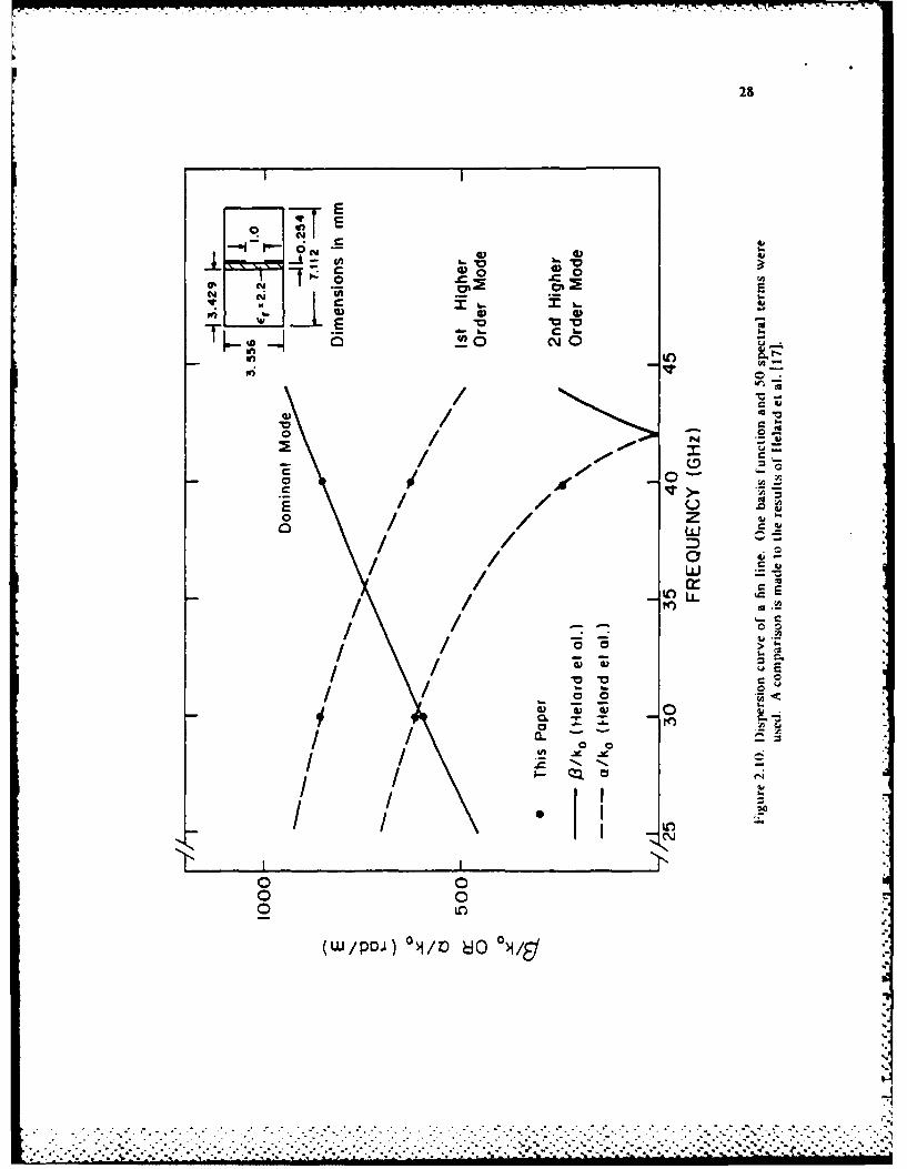
Next, we would like to find modes in a fin line. This is done, as explained earlier, as
a check on the microstrip mode calculations. Results for the first three higher-order modes
are shown in Figure 2.10. and are compared to those of Helard et al. [17]. From this figure.
it is readily apparent that there is excellent agreement between the fin line modes. This
leads us to have a high degree of confidence in our microstrip evanescent modes.
Finally. we present field plots for the first five modes of a microstrip. Since a given
field component is either purely real or purely imaginary, we have plotted the part of the
field that is nonzero. In Figures 2.10-2.13, we have plotted the six components of the
dominant mode of a shielded microstrip. Note that these plots satisfy the boundary
conditions that E-fields tangential to a conductor and H-fields normal to a conductor are
zero. Note also the correct singularity behavior at the edges of the strip. In Figures 2.14-
2.17. we have plotted E, (x .y) and EY (x ,y) for the next four higher-order modes of the
same configuration. These are evanescent modes for the dimensions and frequency given.
Again. we note that the correct boundary conditions and singularities are observed.
° •.
.......
26
0 LO
0C a'j
CLC
2 -
I t-
I -0
(L/ PD)/0 v
27
a 0In a- S~ C
0 1 00
00
ID~~~~l E C 0 - ~'
,-j 2, .N
(0 00
(SINH) 30N03dN
28
T'~ a .C.0 .c
c v
N N000,
S CI~
* a.) Ea a
U, I0'IiO
(L/pj)Iv /
29
Figure 2.11. Plots of E, (x .y)and E, (x .v for the dominant mode of a microstrip. Forthis plot, h-=0.4445 mm. b-=0.381 mm. t -0.127 mm. s -0.0635 mm.
C,=9.6 mm. f req - 20 Glz. and ~3=1037.01 rad/ m.
- .
. - -- S S . . . .T.
30
fi'Liure 2.12. 11 and Hf 1,,d.min~ini m ,,ie :.r it!-ime configurauon .1' Oiai in hl''ure
2.1 1
%.
31
i~u -e 2.13. h anti i ,I !he Jomninl m( tic I r the ' ame configuration -is that. in I i:ure2 11
. .. %
32
I or tht, mode. 13 --40,. 72 rad mi.1 ~ue2 1 4 F. and h ol [tie econd mkI !or ihe a me :ornil-u ralio'n a,.1L :tn F igure 2.9
33
,, /
'NN
'N
/1 -
i // fN -. A
/
K / , / / ~
K -~ . iN. ' N
- - A
7S.
~1~~~
u re 2.15 A anti I: the third n0de r the '~ me n~i~urat nfl ts I hat rn 1,~ure 2.''.[(Jr 'hIS mode. 2 = - 1O47~.5 xii m.
...........
. . -. .
34
I !,Lire 2 10. I: aind h: ,,he lour,.h meoie lr am.ire ln~li.Llraiin as Lhat in Lioure 2 ~H-,r -,his mode. 3 11 4004 4 r", m
- - - - - -
35
(
ivu re 2 17 L: and P. )t the fifth mode o ihe 'd.ine i.,nliiuration ai thati in Figure 2.9For tis moeI 3 - ji 4h'7.1 radt m
p ~7:.
36
2.9 Conclusion
In this section we have demonstrated the capability of calculating microstrip
propagating and evanescent modes. This extends the work of previous authors, as very few
results for evanescent modes were previously available. In addition, we have generated
data on characteristic impedance and fin-line modes, all of which confirm the accuracy of
our calculations. Finally. field configurations of microstrip modes have been generated. and
these have been shown to satisfy the necessary boundary conditions.
All of the above suggest a basic agreement of the mode calculations with the
expected results. The next step is to use these results in a mode matching procedure for
calculating discontinuities.
Let us now proceed to the discontinuity calculatiorn.
..
37
CHAPTER 3
DISCONTINUITY CALCULATIONS
3.1 Introduction
The calculation of discontinuities associated with printed circuits has been of
interest for some time. In particular. abrupt discontinuities in the widths of the strips in
the microstrip and in the slots in the fin line seem to offer the best hope for solution, and
have been studied by a number of authors.
The earliest attempts at solving one of these types of discontinuties occurred in the
realm of microstrip discontinuities. The methods used involved a quasistatic calculation of
a step discontinuity of strip width (27-30]. Although these methods in general yielded
good results, it must be assumed that at sufficiently high frequencies the quasistatic
approximations will break down.
The next generation of solutions involved approximating the microstrip as a
rectangular waveguide with perfect electric conductors on the top and bottom walls and
perfect magnetic conductors on the side walls [31-34]. Although this method yielded a
frequency-dependent solution, it again is expected to break down at higher frequencies due
to the approximations of the model. Furthermore, there are many printed circuit
discontinuities. such as those in the fin line and strip line, for which no waveguide model is
available.
Another attempt at solving this type of problem was made by Lampe [35]. who
presented a three-region analysis of strip line discontinuities. Recall that the strip line and
- fin line are analogous to the microstrip because of the generality of the spectral domain
immitance approach. as discussed in Section 2.2. In his analysis. Lampe begins by breaking
up a discontinuity into three regions. taking the boundaries of the middle region far enough
away from the discontinuity on either side so that most of the evanescent modes have
decayed enough to become insignificant. Next. he finds the dominant and first few higher-
2.o- °
. -... .".,- -.. . ..- ',, -.. .....".-' '..-- -- -...- '-.... -...-.. '> ,,, -.-. '.'>.---.° -. :-i-'
"......... . . ., .. I~'
38
order modes in the first and third regions. Finally, he formulates an integral equation that
relates the magnitude of the mode coefficients in the first and third regions to the unknown
current on the strip in the second region. The solution to this integral equation yields the
desired reflection and transmission coefficients. This method has limitations also, because it
is formulated for an isotropic medium. The strip is assumed to be printed on a thin
dielectric substrate; so thin that it is felt to have little effect. Thus. the entire problem is
formulated in a homogeneous region whose dielectric constant is the volume average'
dielectric constant. This turns out to be a small perturbation from the free-space dielectric
constant of one. This method is appropriate for low frequencies in the strip line, but it
seems likely to break down for higher frequencies. In addition, it is not appropriate for a
microstrip configuration. in which the dielectric material plays an important role. Finally.
this method can not easily be modified to account for the dielectric, since the Green's
function in the second region would then become too complicated.
The most recent attempts at solving this type of problem have occurred in the area
of fin line discontinuities. The methods used in these cases all involved finding a number of
modes for each guide by using a spectral Galerkin method. These modes were then used in
either a mode matching procedure [17.36,37] o- in an iteration procedure [38] to equate the
fields tangent to the plane of the discontinuity.
The results generated in these mode matching papers were not conclusive, but they
did suggest that further study would be in order, and that the method might be applicable
to a shielded microstrip as well as to the fin line. This will be the topic of study for this
chapter.
3.2 Mode Matching
The structure to be analyzed is shown in Figure 3.1a. It involves an abrupt
discontinuity in the strip width of the center conductor of shielded microstrip. whose cross
section is shown in Figure 2.1.
..............................................
39
2 s0
a 2 Sb
2521
2s,3 2 Sb
c -2 1- 2 sc
E~ure I \ mr1lu micri'strr ip Is,.(ofhnuaite' in th ik enler conducior
S. . . . . . . . . . . . . .
40
We begin the analysis by generating the propagation constants and field
configurations for the dominant and first few higher-order modes of each of the two
waveguides. This was discussed in Chapter 2. Next. we express the fields in waveguide A
as a sum of the waveguide modes
"0(x .y z) = . ,a (x.y ) e z (3.1a)".1
Ra (x .y .z) = " a1A 0 (x .y ) e-"" (3.1b)I i=1
where the a, are mode coefficients. -y., are the complex propagation constants of the ith
mode, and 4',, and R,, are the vector mode functions of the ith mode, where
eo, (x .y) = e,,. (x .y )V + e,,, (x .y (3.2a)
F, (x y (x .y )i + h,,,, (x .y (3.2b)
Similar expressions are formulated for waveguide B by replacing "a" with *b" in the above
equations. If we assume the discontinuiLy occurs at z - 0. we may equate the field
components tangential to the interface at z - 0 as
(I1 +p)r, n(x .y ) + E a, 91, (x .y )=tb, t"b (x .y) (3.3a)
=2 11
(l-P). i( .y a R. , (X .Y= b, ,, (X .Y) (3.3b)-' =2 4 =1
This is the equation that is to be solved for the mode coefficients a, and b, and for the
reflection coefficient p.
To solve this equation. we take the inner products of Equation 3.3a with F., (x .y).
and the inner product of Equation 3.3b with ',, (x .y). The inner product is defined as
:,, f f ,,(x.y)xfib,(x.y) dx dy (3.4)S
It is calculated most simply in the spectral domain, in a manner analogous to the power
• o . o . .. .° . . .
,, -"L-- . .."- ..-L. ' ,
;'i '
k I...... .... i. I I I I II
[, . o . . .
41
calculation described in Section 2.5. Thus. the integration over x becomes a sum over
spectral terms. and the integration over y is analytic in the spectral domain. After taking
these inner products. we find
L L-P l 1., E a.. + E b, =a lam m .. L (3.5a)
i =2 iml
L LP Ibma+ E a, 'b,.j + Z bi bmbi bma I m1.L (3.5b)
=:2 i :
This equation can also be written in the form
Ax = b (3.6)
where A is a 2L x 2L matrix of inner products. x is the 2L X I vector containing the
unknown mode coefficients. and b is a known 2L X I matrix of inner products. This can be
solved by a standard linear equation solution routine.
The solution to this matrix equation contains within it the reflection coefficient, p,
and the magnitude of the transmitted wave. b 1. From p. we may calculate an equivalent
circuit of the form shown in Figure 3.2. If we let
p= p, + j p, (3.7)
where p, and pi are both real. then
-( ZN = - (3.8a)Z 1 -21 -pi2
-- I 1 - 2p
P + 1 12 (3.8b)
These parameters are useful because they can be checked with other, more approximate
methods. Therefore. we expect ZN Z,, /Za where Zob and Z, are the characteristic
impedances of the second and first waveguides. as calculated in Section 2.5. Furthermore.
we may compare our values of Y.v to those generated by quasistatic analysis [29]. We
%. "
42
E7r
*NZN
I iure 3 2 lDimen~oons lor ai ,ingle step ds ntuiv in strip width and thecorresr nding equliv-alent circuit.
..................................................... . . . . . .. . . . . . . . . . . S ~S. %
43
should expect only approximate agreement. since we are now using a frequency dependent
method to generate the solution.
A second check we can make on our final answer is to verify that all real power is
accounted for. This is checked by showing that
IS,,i 2 + IS 2 1 12 -- (3.9)
While this condition is not sufficient to guarantee a good solution, it is necessary. and
should be verified.
This concludes the setup of the mode matching procedure. Before we present
calculations, there are a number of related issues that need to be dealt with. These are
discussed in the following three sections.
3.3 Orthogonality of Inner Products
Upon examination of Equation 3.5 we observe a number of inner products of the
form 'aic) where i ; j. We expect the standard orthogonality relationship to hold for the
- normalized modes of uniform waveguides with perfectly conducting side walls [39]
Ia., = f(3.10)
Thus. we are left with the problem of deciding whether or not to retain in the matrix
equation the inner products that are theoretically equal to zero. It must be kept in mind
that our modes have been calculated only to a finite accuracy. dictated by the numerical
accuracy of our methods. If the accuracy in the mode functions is good. then retaining the
cross terms will not matter. If, on the other hand. there is a small error in the mode
functions, then it would seem preferable to retain the cross terms rather than discard what
may be useful numerical information. This is the approach adopted for these calculations.
Oo .
44
3.4 Condition Number of the Matrix
In formulating the mode matching solution, we obtain a matrix equation of the
form Ax - b. A useful parameter associated with this equation is the condition number of
the matrix A. It turns out that if the matrix A has a large condition number, it is very
difficult to obtain accurate solutions for the unknown column vector x.
There are a number of methods that may be used to calculate the condition number
of a matrix, depending on the norm of the matrix chosen for the problem [40,41]. A
reasonable definition of condition number is~.!
IX I (.1C fa ti- IA Ir I .'Co, d (A4=.(~2
manq
where the A's are the maximum and minimum eigenvalues of the matrix AHA and AH is
the transposed complex conjugate of A. If this condition number is large, we have difficulty
in solving the matrix equation. because small errors in the matrix elements generate large
errors in the solution for the unknown vector x. This definition of condition number is .
used in the calculations that follow, in order to check the stability of the matrix equation
solution.
3.5 Matrix Theory for Cascaded Discontinuities
In the case where there are multiple discontinuities. we need a method of keeping
track of a number of modes between one discontinuity and the next. We consider two
cases. First, we study a symmetrical double step. as shown in Figure. 3.1b. This is a
special case of the second case we will study. that of N discontinuities each spaced an
arbitrary distance from the previous discontinuity. An example of this is shown in Figure
3.1c.
In the case of an asymmetrical double step. we may take advantage of symmetry
properties to greatly simplify the problem. Thus. instead of launching the dominant mode
-:.. -.. .
. . . . . . . . . . . . . .. . . . . . . . . .
45
from the left with a magnitude of one, we add the results of launching modes of equal
magnitude and either equal or opposite phase. as shown in Figure 3.3. These cases are
equivalent to placing magnetic and electric conductors at the center of the waveguide B.
The solution for each of these cases may easily be adapted from the solution for the single
discontinuity, since the waveguide modes are reflected from the electric or magnetic
conductor without coupling to other modes. We adapt results from [36] that result in a
slight modification of Equation 3.3. Thus. at z = 0
. "-- (1/2 + p)ro I~x .y )+ .a, (', x .y ) bi 0 + Sbij )er#, (x .y )(3.12a)
i =2=
.oL.I (1/2 - )I(x.y)- , aE°(x'== y , b (I- Sbij ))7b, (x "y) (3.12b:)
where
e for electric conductor at z = I (313)-" -e-2'a" for magnetic conductor at z = 1
and yeb, is the complex propagation constant of the ,th mode in waveguide B. and 21 is the
distance between the discontinuities. The above equation may be solved in a manner
analogous to Equation 3.3 by taking appropriate inner products. as described in Section 3.2.
If. on the other hand. we do not have the luxury of having favorable symmetry
properties. we have to solve the more general case of N discontinuities. each separated by a
length of transmission line. In this case we will have to cascade the generalized S-
parameters of each of the discontinuties. and the transmission lines that separate them, to
form an S matrix for the entire structure. The method that follows is adapted from a
method by Hall [421.
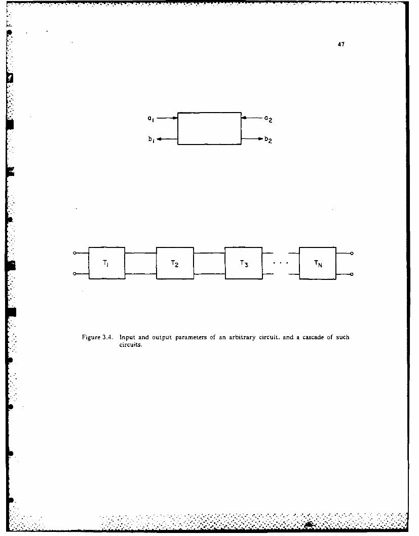
Let us begin with a definition of generalized S- and T-parameters. For the arbitrary
circuits shown in Figure 3.4. we define generalized T- and S-parameters as
... . .
46
A 8
iL7J EiI 1 - E l ElectricI Conductor
I MagneticI Conductor
I:igure 3.3 Symmetrical discontinuities. and the method (i taking advantage of the
symmetr. Ir svmmetrical and antis% rnmetrical excitation ot the
d ison I in u it'.
i b - - . ..i. - i| - -. . .. .
47
a (32Sb, ------- b2
T, T2 T 3 .• . T N
o-.-
Figure 3.4. Input and output parameters of an arbitrary circuit, and a cascade of suchcircuits.
....... , , , . -. . . . . . .
48
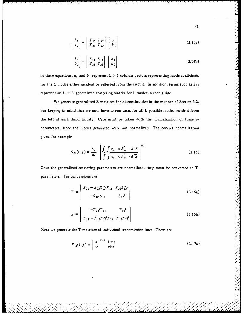
b2 T11 T12 a, (3.14a)a2 T21 T22 b
b2 S21 S22 a2 (3.14b)
In these equations. a, and b, represent L x 1 column vectors representing mode coefficients
for the L modes either incident or reflected from the circuit. In addition, terms such as S 11
represent an L x L generalized scattering matrix for L modes in each guide.
We generate generalized S-matrices for discontinuities in the manner of Section 3.2.
but keeping in mind that we now have to run cases for all L possible modes incident from
the left at each discontinuity. Care must be taken with the normalization of these S-
parameters, since the modes generated were not normalized. The correct normalization
gives, for example
S21( = (3.15)a, f frX~ 'd.
Once the generalized scattering parameters are normalized, they must be converted to T-
parameters. The conversions area
S 21 ~S22S 1-1S 11 S 22S 12T =-1 (3.16a)-S I S 11 12l /
s (3.16b)-1 T"12 Tj-21T2 1 T12T 22'
Next we generate the T-matrices of individual transmission lines. These are
e i=j (3.17a)T11(i.j) = 0 else
.. . . . .. . .. . - -.-
. . . . . . . . .. . . . . . . . . . . . . . . . . . . . . . . . . . .. .. . .. . . . . . . . . . . .. o
. . . . . . . . .. . . . . . . . . . . . . . . . . . . . . . . . . . .
49
i e jyA i~. (3.17b)~T22(i 'J)= 0 else
T 12 = T 21 =0 (3.17c)
Finally. we cascade a number of discontinuities and transmission lines by multiplying the
T-matrices together to obtain a composite T-matrix for the entire structure of N
components. as shown in Figure 3:4.
T = T N • TV -1 ..•. T2 • T, (3.18)
This is now converted to an S matrix using Equation (3.13b). and the problem of cascaded
discontinuities is now formulated. Numerical results for single and cascaded
discontinuities appear in the next two sections.
3.6 Results for the Single Discontinuity
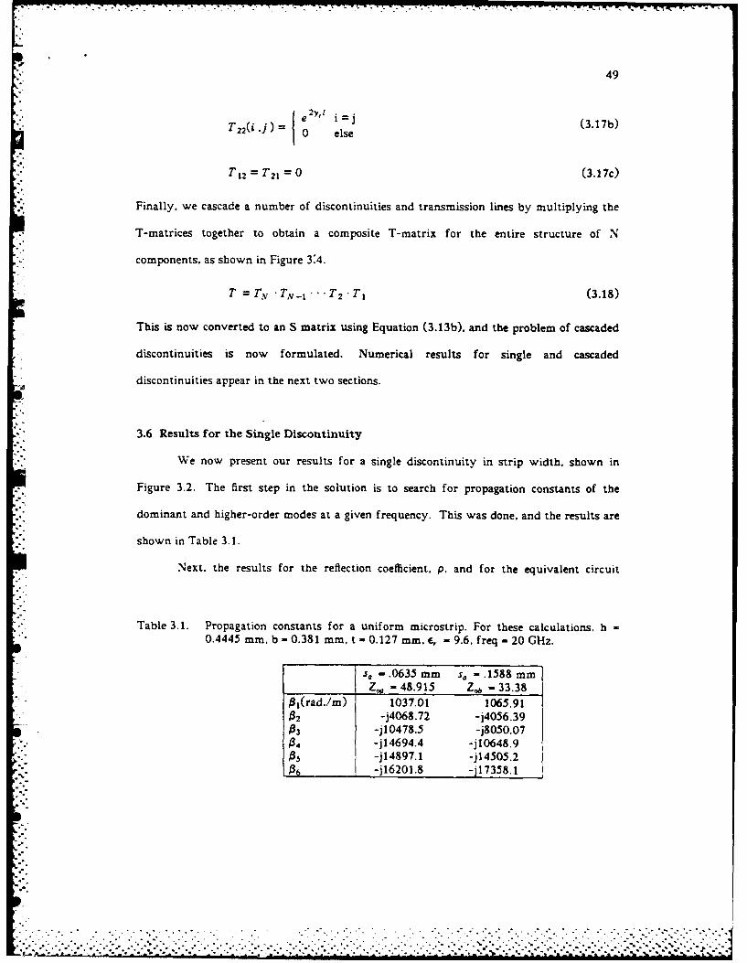
We now present our results for a single discontinuity in strip width, shown in
Figure 3.2. The first step in the solution is to search for propagation constants of the
dominant and higher-order modes at a given frequency. This was done. and the results are
shown in Table 3.1.
Next. the results for the reflection coefficient. p. and for the equivalent circuit
Table 3.1. Propagation constants for a uniform microstrip. For these calculations. h -
0.4445 mm. b - 0.381 mm, t - 0.127 mm. er - 9.6. freq - 20 GHz.
s. =.0635 mm so = .1588 mmZ , -48.915 Z, - 33.38
" 1(rad.!m) 1037.01 1065.9102 -j4068.72 -j4056.39033 -j10478.5 -j8050.0704 -j14694.4 -j10648.9
-j14897.1 -j14505.2086 -j16201.8 -j17358.1
.-.. . . . . .
"'" '" ' " '". .'.". .".. ." '". . . ." " " " " " " . . . . ' '. ' ' ' ' ' " " " " " " " " "
50
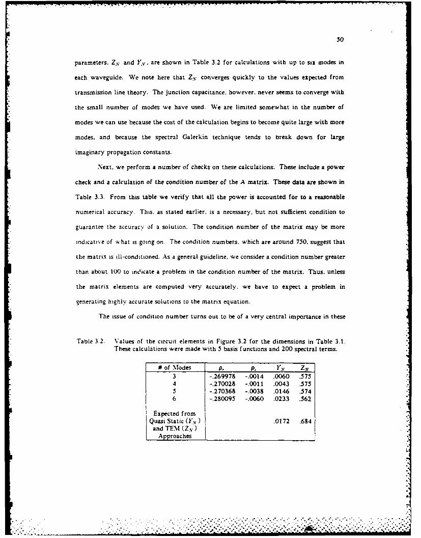
parameters. ZN and Y.V. are shown in Table 3.2 for calculations with up to six modes in
each waveguide. We note here that ZNv converges quickly to the values expected from
transmission line theory. The junction capacitance, however, never seems to converge with
the small number of modes we have used. We are limited somewhat in the number of
modes we can use because the cost of the calculation begins to become quite large with more
modes, and because the spectral Galerkin technique tends to break down for large
imaginary propagation constants.
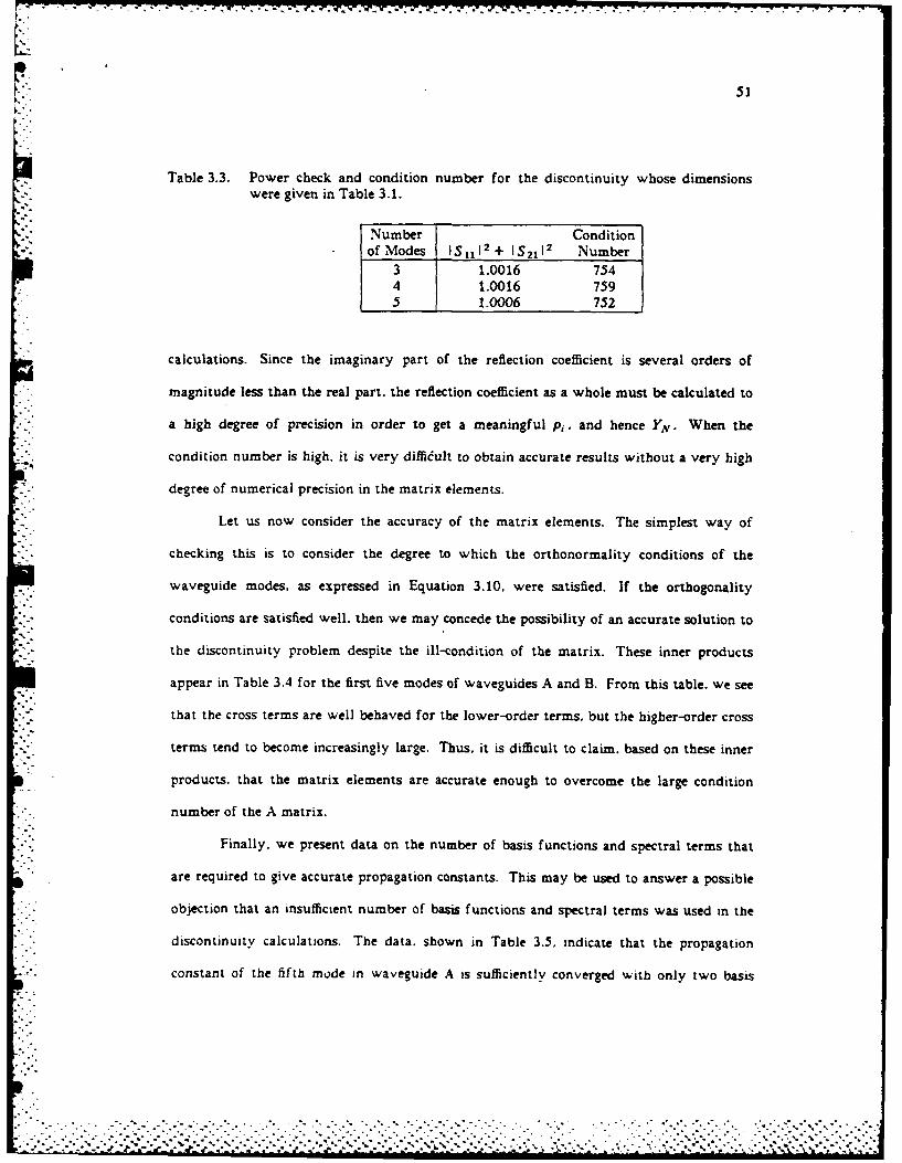
Next. we perform a number of checks on these calculations. These include a power
check and a calculation of the condition number of the A matrix. These data are shown in
Table 3.3. From this table we verify that all the power is accounted for to a reasonable
numerical accuracy. This, as stated earlier, is a necessary. but not sufficient condition to
guarantee the accuracy of a solution. The condition number of the matrix may be more
indicative of Ahat is going on. The condition numbers, which are around 750. suggest that
the matrix is ill-conditioned. As a general guideline. we consider a condition number greater
than about 100 to indicate a problem in the condition number of the matrix. Thus. unless
the matrix elements are computed very accurately, we have to expect a problem in
generating highly accurate solutions to the matrix equation.
The issue of condition number turns out to be of a very central importance in these
Table 3.2. Values of the circuit elements in Figure 3.2 for the dimensions in Table 3.1.These calculations were made with 5 basis functions and 200 spectral terms.
# of Modes p,. P, Yv Zv3 -.269978 -.0014 .0060 .5754 -.270028 -.0011 .0043 .5755 -.270368 -.0038 .0146 .5746 -.280095 -.0060 .0233 .562
Expected fromQuasi Static (Y.v) .0172 .684
and TEM (Zv)"Approaches -
W , %~
.','.'..*-*.
....-.... .. O F. • .
51
Table 3.3. Power check and condition number for the discontinuity whose dimensionswere given in Table 3.1.
Number Conditionof Modes 'S11I2 + IS 2 1 12 Number
3 1.0016 7544 1.0016 7595 1.0006 752
calculations. Since the imaginary part of the reflection coefficient is several orders of
magnitude less than the real part. the reflection coefficient as a whole must be calculated to
a high degree of precision in order to get a meaningful pi. and hence Y1N. When the
condition number is high, it is very diffieult to obtain accurate results without a very high
degree of numerical precision in the matrix elements.
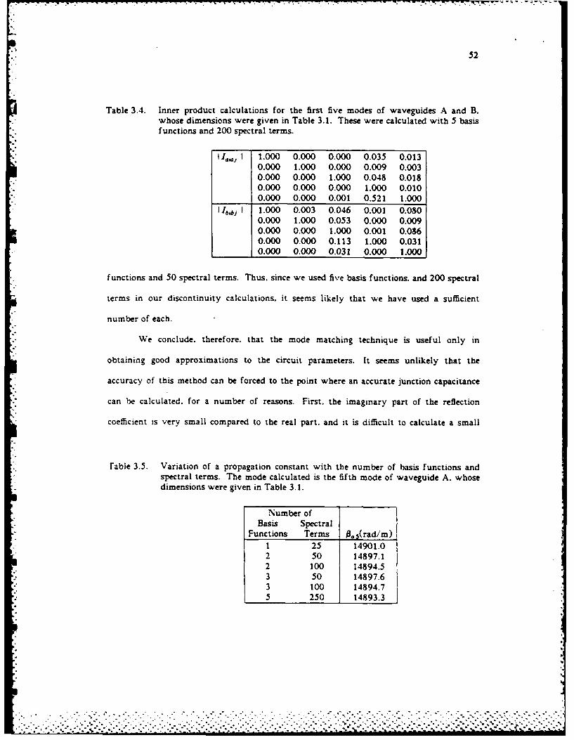
Let us now consider the accuracy of the matrix elements. The simplest way of
checking this is to consider the degree to which the orthonormality conditions of the
waveguide modes, as expressed in Equation 3.10. were satisfied. If the orthogonality
conditions are satisfied well. then we may concede the possibility of an accurate solution to
the discontinuity problem despite the ill-condition of the matrix. These inner products
appear in Table 3.4 for the first five modes of waveguides A and B. From this table, we see
that the cross terms are well behaved for the lower-order terms, but the higher-order cross
terms tend to become increasingly large. Thus. it is difficult to claim, based on these inner
products. that the matrix elements are accurate enough to overcome the large condition
number of the A matrix.
Finally, we present data on the number of basis functions and spectral terms that
are required to give accurate propagation constants. This may be used to answer a possible
objection that an insufficient number of basis functions and spectral terms was used in the
discontinuity calculations. The data, shown in Table 3.5. indicate that the propagation
constant of the fifth mode in waveguide A is sufficiently converged with only two basis
• °>
52
Table 3.4. Inner product calculations for the first five modes of waveguides A and B.whose dimensions were given in Table 3.1. These were calculated with 5 basisfunctions and 200 spectral terms.
' Ilj I 1.000 0.000 0.000 0.035 0.0130.000 1.000 0.000 0.009 0.0030.000 0.000 1.000 0.048 0.0180.000 0.000 0.000 1.000 0.010
"__ 0.000 0.000 0.001 0.521 1.000
J Ibi 1 1.000 0.003 0.046 0.001 0.0800.000 1.000 0.053 0.000 0.0090.000 0.000 1.000 0.001 0.0860.000 0.000 0.113 1.000 0.031
1 0.000 0.000 0.031 0.000 1.000
functions and 50 spectral terms. Thus. since we used five basis functions. and 200 spectral
terms in our discontinuity calculations, it seems likely that we have used a sufficient
number of each.
We conclude, therefore, that the mode matching technique is useful only in
obtaining good approximations to the circuit parameters. It seems unlikely that the
accuracy of this method can be forced to the point where an accurate junction capacitance
can be calculated, for a number of reasons. First. the imaginary part of the reflection
coefficient is very small compared to the real part. and it is difficult to calculate a small
rable 3.5. Variation of a propagation constant with the number of basis functions andspectral terms. The mode calculated is the fifth mode of waveguide A. whosedimensions were given in Table 3.1.
Number ofBasis Spectral
Functions Terms o s(rad/m)1 25 14901.02 50 14897.12 100 14894.53 50 14897.63 100 14894.7
1 5 250 14893.3
.-.
" " - ' -' "--- . ' " " .- ." .- - " . .. '-- -- .. . ' '.". " .-- '." -" - .."- .-' ---. . . . . . -"- . "- -"-. -'- -"----. .'"'. . .- . . , . . .. . .. ...... . ..,,... ..-.-.-. ...- .. ,.. .. ....- .. :q ... ... .-.... ,. . .-. , . , ., , ,, - ,- ,,. - , ,-,
'. T-h -".
53
quantity in the shadow of a larger effect. Second. the condition number of the matrix
indicates an instability in the matrix that can only be overcome if the matrix elements are
calculated to a high degree of accuracy. Finally, the inner product calculations suggest that
the matrix elements can only be calculated to a finite degree of accuracy and that the
spectral Galerkin technique can not be pushed beyond this point for modes of high order.
With these thoughts in mind. let us now turn to other discontinuities to calculate.
Although we have not achieved a high degree of accuracy in the calculations for the single
discontinuity, we have demonstrated that the method generates a good approximation for
the solution. Thus. there may well be reason to consider other types of discontinuities. and
results for these are presented in the section that follows.
3.7 Results for Other Discontinuities
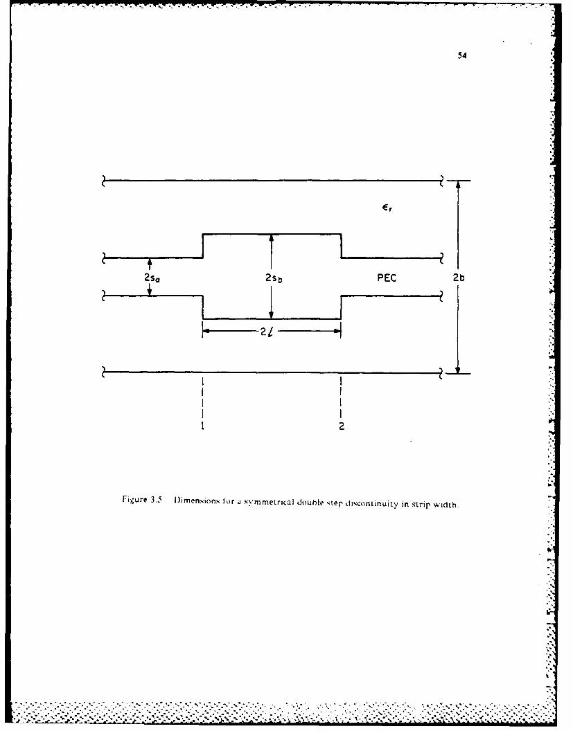
The next configuration we would like to study is the symmetrical double step
discontinuity. This is shown in Figure 3.5. and the theory was presented earlier in Section
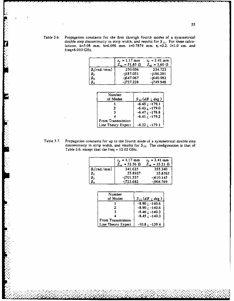
3.5. Results are presented for a typical case at two different frequencies in Tables 3.6 and
3.7. These calculations were made with up to four waveguide mode functions in each
waveguide. Upon examination of these results, we find the reflection coefficient has
converged nicely within four modes to a result that is similar to that expected from the
transmission line theory. We note. furthermore, that the results for one mode are similar
to that for four modes, so in the future we need to use only a single mode for our
calculations.
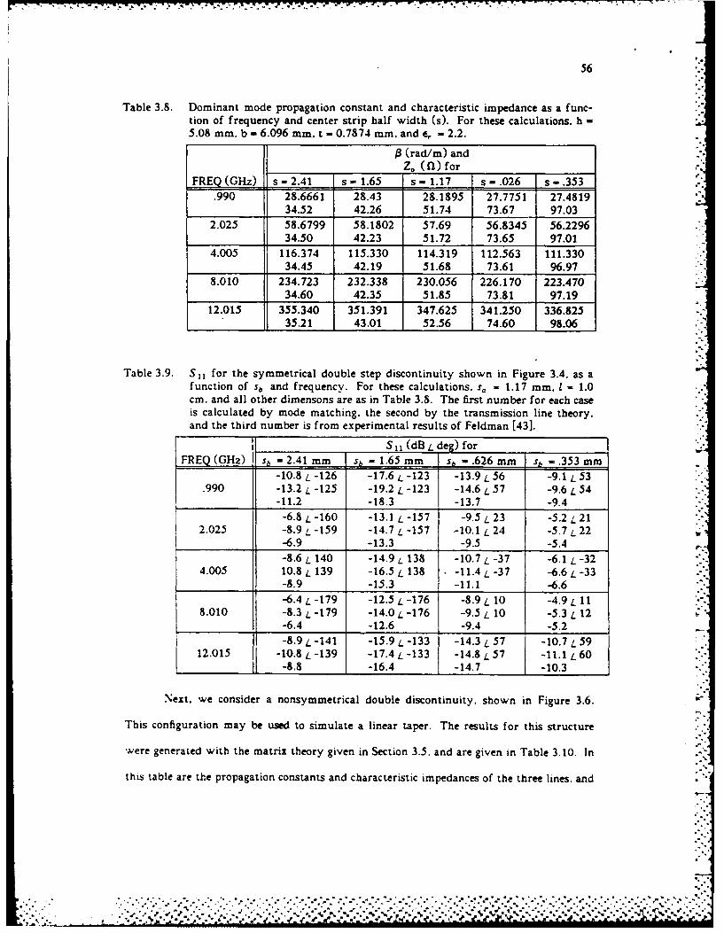
In the next two tables, Tables 3.8 and 3.9. we present data for several of these cases
over a range of frequencies and for various values of Sb. We compare them to experimental
data. which was generated by U. Feldman [43]. and to results generated by the transmission
line theory. Based on the data in these tables. we observe that the data calculated by the
mode matching technique provide a slightly better fit to the experimental data than the
results generated by the transmisison line theory.
t%
54
Er
2so 2 sb PEC 2
1 2
Figure 3.5 D~imensions bor a symnmetrical double ;ter discontinuity mn strip width.
55
Table 3.6. Propagation constants for the first through fourth modes of a symmetricaldouble step discontinuity in strip width. and results for S 11. For these calcu-lations. h-5.08 mm. b-6.096 mm. t-0.7874 mm. e,. -2.2. 1-1.0 cm. andfreq-8.010 GHz.
1 1(rad./mm) 230.056 234.723t32 -j187.051 -jI86.281f33 -j647.067 -j640.983t34 -j727.228 -j749.948
Numberof Modes S 11 (dB L deg)
3 -6.47 L -178.84 -6.41 L -179.2
From TransmissionILine Theory Expect -8.32 L -179.11
Table 3.7. Propagation constants for up to the fourth mode of a symmetrical double stepdiscontinuity in strip width, and results for S I. The configuration is that ofTable 3.6. except that the freq - 12.02 GHz.
s,- .7 mm sb 2 .4 1 rnln___Z__ ,. -25256 fl Z,~ - 35.21 fl
0 1(rad./mm) 341.625 355.3400255.8937 55.8765
033 -j701.537 -j610.145t34 -j723.682 -j904.769
Numberof Modes S 11 (dB L deg)
1 -8.90 L -140.6
4 -8.45 L -140.3From Transmission
ILine Theory Expect -10.8 L -139.4_
56
Table 3.8. Dominant mode propagation constant and characteristic impedance as a func-tion of frequency and center strip half width (s). For these calculations. h .5.08 mm. b - 6.096 mm. t - 0.7874 mm. and E, - 2.2.
0 (rad/m) andZo (fn) for ,-.
FREQ (GHz) s - 2.41 s - 1.65 s - 1.17 s - .026 s = .353.990 28.6661 28.43 28.1895 27.7751 27.4819
34.52 42.26 51.74 73.67 97.032.025 58.6799 58.1802 57.69 56.8345 56.2296
34.50 42.23 51.72 73.65 97.014.005 116.374 115.330 114.319 112.563 111.330
34.45 42.19 51.68 73.61 96.978.010 234.723 232.338 230.056 226.170 223.470
34.60 42.35 51.85 73.81 97.1912.015 355.340 351.391 347.625 341.250 336.825
35.21 43.01 52.56 74.60 98.06
Table 3.9. SII for the symmetrical double step discontinuity shown in Figure 3.4. as afunction of sb and frequency. For these calculations. s, - 1.17 mm. I - 1.0cm. and all other dimensons are as in Table 3.8. The first number for each caseis calculated by mode matching. the second by the transmission line theory.and the third number is from experimental results of Feldman [43].
S11 (dB Ldeg) for _'"
FREQ (GHz) sh - 2.41 mm st - 1.65 mm sh - .626 mm sb - .353 mm-10.8 L -126 -17.6/L -123 -13.9 L 56 -9.1 L 53
.990 -13.2 _ -125 -19.2 L -123 -14.6 L 57 -9.6 L 54-11.2 -18.3 -13.7 -9.4-6.8/- -160 -13.1 L -157 -9.5 L 23 -5.2L 21
2.025 -8.9 L -159 -14.7 L -157 -10.1 L 24 -5.7/- 22 "-6.9 -13.3 -9.5 -5.4-8.6 L 140 -14.9 L 138 -10.71 -37 -6.1 L -32
4.005 10.8 L 139 -16.5 L 138 -11.4 L -37 -6.6 L -33-8.9 -15.3 -11.1 -6.6
-6.4 L -179 -12.5 L -176 -8.9 L 10 -4.9 L 118.010 -8.3/ -179 -14.0 L -176 -9.5 L 10 -5.3 L 12
1 -6.4 -12.6 -9.4 -5.2
-8.9 L -141 -15.9 L -133 -14.3 L. 57 -10.7 L 5912.015 -IO. 8 L- 3 9 -17.4 L- 13 3 - 14 .8L57 -11.1 6 0
- -8.8 -16.4 -14.7 -10.3 -
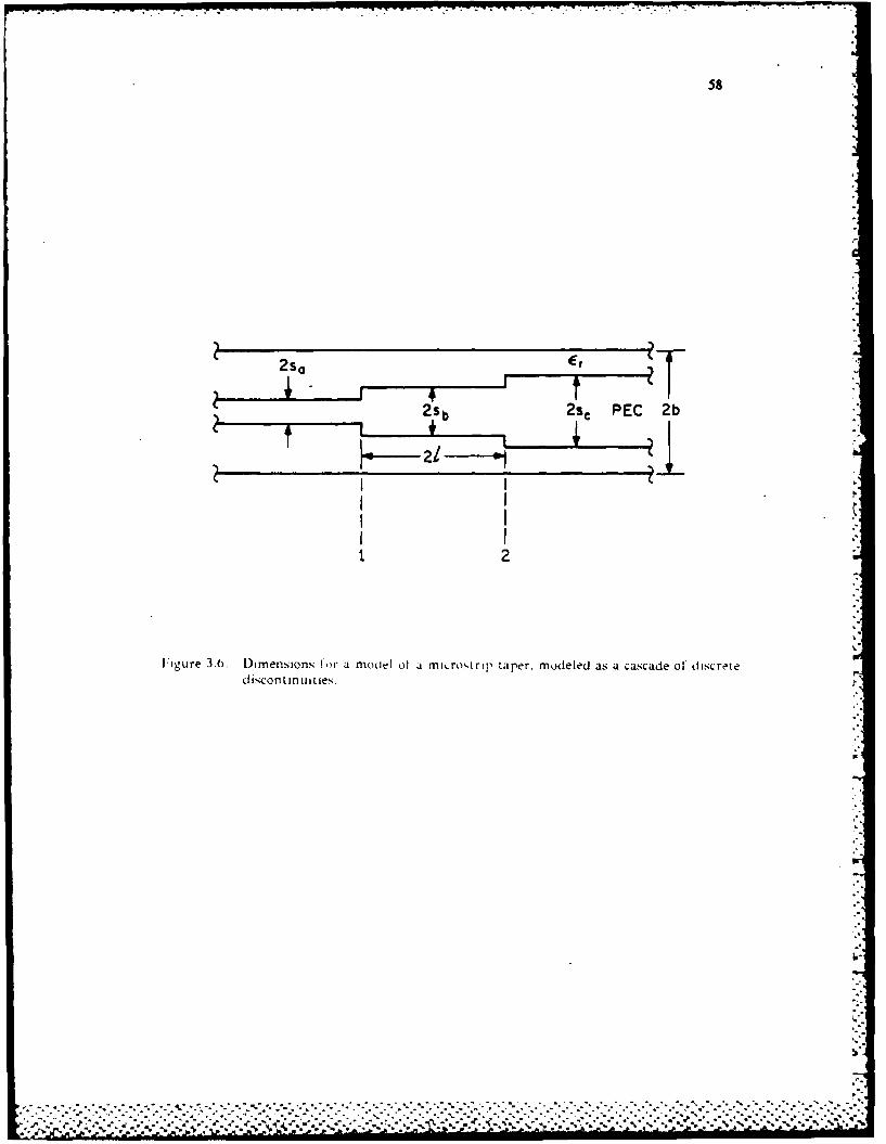
Next, we consider a nonsymmetrical double discontinuity, shown in Figure 3.6.
This configuration may be used to simulate a linear taper. The results for this structure
were generated with the matrix theory given in Section 3.5. and are given in Table 3.10. In
this table are the propagation constants and characteristic impedances of the three lines, and
- ..A
57
the S-parameters of the discontinuity referenced to planes Nos. 1 and 2 as shown in Figure
3.6. In addition. Table 3.10 has a comparison to transmission line theory and a power check
of the mode matching results. The results indicate an overall agreement with the
transmission line approach. although it is difficult to say which approach is more accurate.
Finally, we consider a single discontinuity in the dielectric constant, strip width.
and substrate thickness, a diagram of which is shown in Figure 3.7. This case is one that
might be expected to occur when a microstrip printed on gallium arsenide must mate with a
microstrip printed on duroid board. Because of the difference in dielectric constants. it will
be necessary to have different line widths to maintain a 50 ohm line in each section. Some
typical S-parameter data for this configuraton are shown in Table 3.11. along with data for
a power check and the condition number of the matrix. These data are difficult to interpret
since the condition numbers are very large. and since the power check is off by about 0.06.
Both transmission lines are 50 ohm lines, so we expect a reflection coefficient of zero from
simple transmission line analysis. while we calculate a reflection coefficient of about -10 dB.
This -10 dB reflection corresponds to a value of 0.1 in the power check. Since the power
check is off by 0.06. it is difficult to get a feel for the accuracy of these results. If we
* . ignore. however, the higher-order modes, and look only at the results when a single mode is
,' . used. we still have a reflection coefficient of about -10 dB. but now the power check and
condition number of the matrix are both satisfactory. It appears. therefore. that
experimental work will be required to verify these calcLlations.
3.8 Conclusion
In this chapter we have analyzed a number of discontinuities by using a
combination of the spectral Galerkin technique to generate modes and mode matching to
find the scattering parameters of the discontinuity. In general. our results have been close
to what was expected. but it proves difficult to use this technique to give highly accurate
results. The factors that limit the accuracy include the small number of waveguide modes
... ........... . . . . . . ... .. . . .
.?... .-...-..-."...'..........-..........°...-....,.... .. ..-.-........ . . .....'-.,-.-,....... ..- '...",..,".--.-.-...'... ...': -,[~~~~~~~~~~~~~~~~......,.......-.,,. ... ,.,.,........... .. ,...,....•........-,-.-.... ...-...-. ,. , ... . .. ,.,,,.
"t•" i i i i ll.. .. . . . . . . . . . . . . .. . . . . .. . .. .
58
2S s E 2--
22
Figure 3.0. Dinmensions I'm a rnoota of a MILrostrtr taper. modeled as a cascade of discretediSCOntinUILIeN.
...............
- 4 o * %.
59
Table 3.10. Results for the taper simulation shown in Figure 3.6. For these calculations.h = 5.08 mm. b = 6.096 mm. t = 0.7874 mm. e, - 2.2, and I - 1.0 cm.
_ _ _ _ _ _ 10 GHz 12.5 GHz 15.0 GHz
s - 1.17 mm 0. (rad/m) 288.2 261.8 435.9Zo' (fl) 52.14 52.j7 53.28
Sb = 1.65 mm Ob 291.2 365.7 440.8Zb 42.63 43.11 43.67
s. = 2.41 mm Pc 294.36 269.9 445.9Z 34.86 35.30 35.79
Transmission S12 -14.95 L - 154 -1 9 .7 6 L 122 -15.81 L -1 4 6
Line S21 -0.14 L 26 -0.05 L -59 -0.12 L -146Theory S22 -14.95 L 26 -19.76 L -59 -15.81 L 34
dB L deg I
Mode S11 -12.78 L - 15 2 - 1 7 .6 1 L 114 - 1 2 .9 4 L -143
Matching S 2 1 -0.23 L 26 -0.76 L -58 -0.18 L -146S22 -12.78 L 23 -17.61 L -51 -13.94 L 31IS1112+ lS 21 1
2 1.00000 0.999998 0.999999
Table 3.11. Results for a step discontinuity in e, . t. and s. For these calculations h, =0.889 mm. hb - 0.953 mm. b - 1.27 mm. t, = 0.127 mrxi. tb = 0.191 mm. s. =
0.042 Mm. Sb = 0.298 mm. 6,, = 12.3. e'b = 2.2. freq. = 20 GHz. These calcu-lations were made with 2 basis functions and 50 spectral terms, andZ, = Z = 50.0 (1.
Number Conditionof Modes S 11 (dB Ldeg) S, (dB Ldeg) IS,,12 + IS2112 Number
I -9 .9 2 / 180 -. 4 6 L 0.0 1.00000 262 -1 1.6 9 L -175 -.08 L -2.2 1.066 62403 -11. 6 7 L- 1 7 5 -. 0 1 L -2.0 1.066 67904 -11. 6 7 L- 172 -. 0 2 L -3 .2 1.063 6800 ,
.2.
. . .... •
.° . . .. . .-.. -. ".-.. .... o... .. ,. .,.o.... .,- .. o ..
.. . . . . . . °- ,•. o. -. .' -o . .. o ° o' - , . , . % - '° . , % -
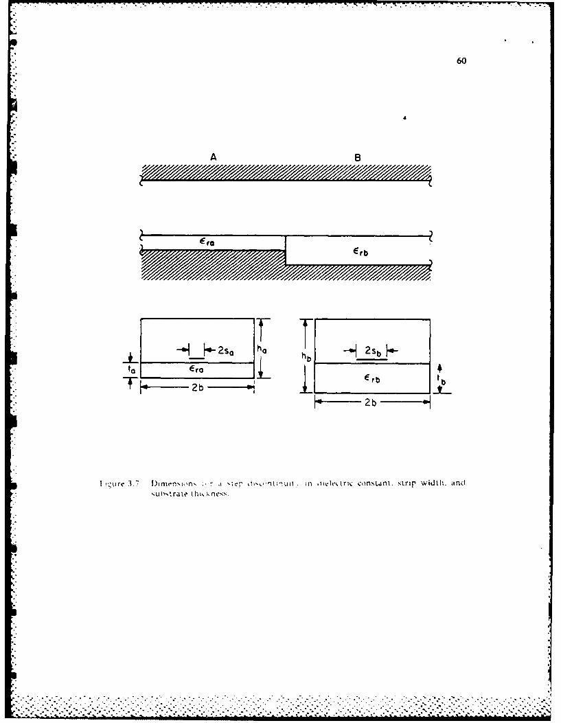
60
A B
.1 Era
T Erb tb
U 2re -3 7 tDirnen,,n, .1 '.:er d'.n.uIII OInICeLtric constint. ,trlr width. aind
. . . ... . . . .
61
one can calculate with the spectral Galerkin technique. the ill-condition of the set of matrix
equations, and the necessity of calculating a small junction capacitance in the shadow of a
comparatively large reflection coefficient.
If this method is to be refined to yield more accurate results, we have to find a way
to generate a large number of very accurate waveguide modes. In the next chapter. we
consider an alternate method of generating these modes, in an effort to increase the accuracy
of the mode matching method. Let us now turn our attention to the singular integral
equation technique.
.... ,-
.-. ,
. . . . . . . . . . . . . . . . . .. . . . . . . . . . . . . . . . . . .
62
CHAPTER 4
THE SINGULAR INTEGRAL EQUATION TECHNIQUE
4.1 Introduction
The singular integral equation technique is an alternate method of finding modes in
printed circuit waveguides. This method was first suggested by Mittra and Itoh [5]. and has
since been expanded upon by Omar and Schunemann [44.45]. Its chief advantage over the
spectral Galerkin method is its very high degree of numerical efficiency. requiring, by
comparison, very little computer time. Its disadvantage, however, is that it is a much more
difficult method to derive and implement. requiring a great deal of effort to derive the
matrix equation.
In this chapter, we outline the work of Mittra and Itoh and expand upon it by
calculdting a larger number of terms in certain series as well as a larger matrix size. In
addition, we compare these results to those obtained with the spectral Galerkin technique
presented earlier.
4.2 Overview of the Method
In this section we outline the singular integral equation technique as applied to the
microstrip. and as explained in (51. Since the method is somewhat involved, we omit a
number of details here that are included in [5]. In spite of this. we include sufficient detail
to demonstrate the reasons for the increased efficiency of the method.
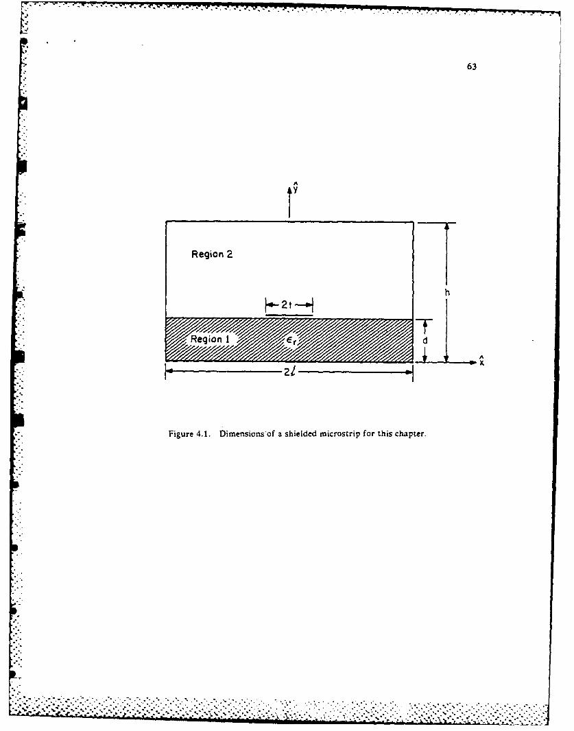
Consider the shielded microstrip structure shown in Figure 4.1. We may write the
fields in the two regions, denoted by i. as a sum of TE and TM components. This leads to
k 2 3 o2 ,(e )e -J 6z (4. la)
" , e -J 3 (4.1b)
. . ., ..
,. . .,_, . . . ... , , .'..-..~~~~~~~~......... ...,. - .. ...' ........., . ..' _.. ,..,,.- '.'.... .. .. . . ,. .
63
Region 2
T
Figure 4. 1. Dimensionsof a shielded microstrip for this chapter.
64
- 7, 2 V r()e -j z (4. 1c)
for the TMI fields and
=z j k?2- p2 0 1 h )e-j Az (4.2a)
T~(h .± 2 xV, 4,(" )e 02 (4.2b)
Ar'() , j,(h) e i1 (4.2c)
for the TE fields. In these equations (3 is the propagation constant in the 2direction.
and *jit) are scalar potentials for the E and H fields, respectively. and the subscript t
indicates the transverse direction. The scalar potentials each satisfy a two-dimensional
Helmholtz equation as in Equation 2.2 of the spectral Galerkin approach. where
k, EI~~ is the propagation constant of the medium in regions I and 2. By satisfying
the boundary conditions on the side and top walls, we expand the scalar potentials as
= A,() sinh ci()y cos i, (4.3a)
n =1
= (f ) csih a,(1)y sin k- x o (4.3b)nj
1: B,( coha2 -h y sink~ (4.3d)
where
.(n 12)1- (4.4)
of1) 2 k (4.5a)
65
an -r . (3 - k02 (4.5b)
and k0 =
We may now apply the boundary conditions at y - d. which is the interface of the
two regions. to obtain
:T,")Cos inx 0. 0 <x < t(4.6a)
;in(,)k in A,(() Coskft x
ft T" Csi x 0 <L (.b
- ,I in si0n . 0 x < L (4.6c)
~ A~',S sin k x
X," AWk sin x =0. 0 < x < L (4.6d)
where
P,,(3)4, -- cotb, I'd + E t2 .a,( 2 ) a( 2 ) -d
1-13 k,,
+,.. coth a (2 (h -d) (4.7a)
f - 0-1
T" ~ ~ , inat Id+ ctha()h d(.b
a7p. n-T
.. *. . . . .. . . . . . . ..-- ~ ...... -... ..
I * m u J nl. ! r' r 'r 4 *4m r . °'.. .. ,. . . -, . ,. ... .. .- . - . .. . . - . ~ r r
66
Qn (j3) = t 1 - coth a(2) (h - d ) (4.7c)
W" (9) = c 4 coth a(I1 d + i coth a2) (h -d) (4.7d)
and 3 -- /ko. This set of equations could be solved in their current form, but there would
be no savings in computation time, since no effort has yet been made to reduce the number
of terms needed for the summation. Let us now consider the method for doing so.
If we differentiate Equation 4.6a with respect to x and substitute the result into
Equation 4.6c. we obtain
A,,Y" sin kfx 0. 0 < x < t (4.8a)
n =1
Next if we differentiate (4.6d) and rearrange. we find
SAftt cos i" x f (x) t < x < L' (4.8c)
E ;T(A ) kf cos kfx g (x). t < x < L (4.Sd)
where
') (am E)+bm:A))cos mx. (4.9a)
(x (cm:T )+ Mnh)cjm (49b.°." (x)= (,,, M'° ) + d,,, g, 1Cos/ x (49b).o=1 m--
and
ain lc P,,(O)W(t)- T(3)Qm()a, = £ 1-P(0)W( )- T(O3)Q(F) (4.1Oa)
- - P' ." -• P--' , ." r '.." "-" ".. . . . .. . . . . . . . . . . . . . . . . . . . . . . . . . . . . . . ..-. . . . . . . .m m l
67
b,,, km T,,, (O)W(0) - T(j)W, (0) (4.lOb)
Cm,, = P(P)Qm (0) Pm (6)Q (0)""m (4.100)PC () W (0J) - r(UT2 07
P(0)Wm (,) - Tm (3)Q (1) (4.10d)dm --km,, I -- P )f3)W(0) - T ()Q(07)
The functions P(03). T(0j).Q( ). and W(P) are the asymptotic limits of Pm(P). Tm (0).
Qm (3). and Wm ( 3). respectively, as m - o. These are
P(P) = 2 E, (4.11a)
T(/3) = 272 (4.11 b)
S(j3) = 2 (4.11c)
I -6
w(p) = 2 + 1 (4.11d)1-i32
It turns out that a,. bm, cm. and d,, can be written in terms of expressions such as P-Pm
and T-Tn . and that these expressions decay rapdily for large m. Thus. for example
P - P, 2Er e -(2m - I)Ird/IL + e - (m - : )wth-d)IL (4.12)
for large m. Since these terms decay very rapidly, the am. b , c,m. and dm coefficients in
Equation 4.9 also decay rapidly. Therefore. only a small number of terms are necessary for
the summations in Equation 4.8. This is the reason that the method is numerically very
efficient.
There is a standard method of solving an equation of the form of Equation 4.8.
which appears in a number of texts [46-49]. as well as in [5]. We therefore forego the
detailed explanation of the solution, and instead quote the result from [5]. The solution to
Equation 4.8 is the following matrix equation.
.*....
. A
68
4(, 8pm a'mD,,. - Mm K)A.
E b.D,,,+ N. Kp)A-(") 0, p =1.2....
S(-"c. D,,. "X.mKq)AA (4.13)
+ (kq8n dn Dqn Yn Kq ) n(A) =0 q 1.2...
where Snm is the Kronecker delta. As before, in the spectral Galerkin technique. the
solution for 13 is found when the determinant of the coefficient matrix vanishes.
Let us identify the missing terms in Equation (4.13). It turns out that
in-1
am q 0 m ' (4.14a)
Mm-
bm E Pmqf (4 4b
where Pis identified by
-ok~ 1 Pm, cos q8 (4.15)cos k x 9 0
and
dO
I f (4.16)
T j cos 9d
f V-d - q =00 1 -0 1 - 2 Cos 8
= Inqsnd 12 r- (4.17)
1 a, - 01) Cos0
NM
69
We note. furthermore. from Equation (4.13) that
Xm= Sm - M QIg - (Qa - Wc )E (4. 1&a)
;-= S - wit (4.18b)
where
" s-sink tS - (W- W, )K, (4.19a)
sin k,(
S 0 sin kt ID ,..(Q Q,)b,,, -(IV W.)d,.+ K(Q -Q.W. (4.19c)
and
g -21 f In - al --C2 € 0S 9 ' + 4 l C 2 dO (4.20)
'(r27f2 q =
""-2" Jo =o n "1- t-a s + !- t - a~ 2 cos ' d- (4.22a
• 1- l a 2 CsOS - r 01 11 a2 1 C - a OS
E, E Pmqv q +P" 1 . (4.21)
where
=. -fIn v + i 1 a odO(4.22a)
VI-i-co s9--fTa+ _1r_,_2,9
= 0n 1 a2 cos + r, -- 01, sin qO' sin G' d9'-' .- J, f In "(4.22b)
-a, - a2 cos 9 - - i - - a2 I t, - a 2 cos 9'
Finally. the last two terms in Equation 4.13 that need to be defined are Kn and Dm. These
I' . - , l i"I . ...... . . . . . ..- . ...
70
are
K 2. cos 1x sink x dx (4.23)
Dnm = COSIX P, sin qO - Pm0 Cos 0 sin x dx (4.24)2.,-- 1ok fl1P si1-P. cosO
T- fw q= sink- dx (24
where the variable 0 is defined by the coordinate transformation
cos . I C2 cosO (4.25)
and
IiI12 o t J(4.26a)This completes the description of the final solution, which was stated in Equation 4.13.
The integrals shown in Equations 4.16 and 4.17 are well behaved, and can be easily
calculated with a numerical quadrature subroutine. The integrals in Equations 4.20 and
4.22. however, have an integrable logarithmic singularity at = 0. We therefore .,ust use
a small angle approximation for cos 9 inside the logarithm in the region 0 < 8' < op.
where Op << 1. and use an integration routine in the region 6, < 9 < 7r.
We now have only to calculate P,,. K,. and D,,,. as shown in Equations 4.15.
4.23. and 4.24. In [5] these terms were calculated only to the second or third order. We
now would like to extend the work of [5] by calculating these terms out to the fifth order.
These are calculated in the next section.
4.3 Calculation of Pmq, K. and D0.,
In reference [5]. Mittra and Itoh calculated P,,. K, and Dn, to the second or third
- .. -~-- - - - -* ..-. - . . .
. . . .. . . . . . . . . . . . . . . . . . . . . . . .
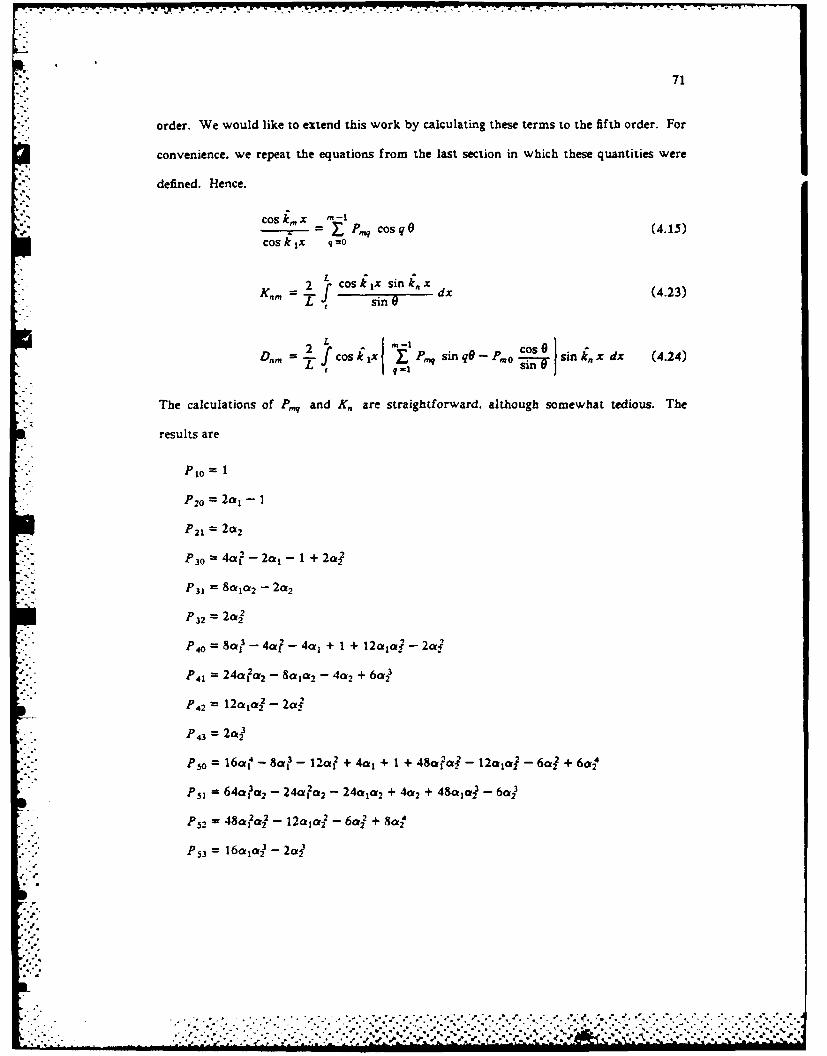
7171
.. 71
order. We would like to extend this work by calculating these terms to the fifth order. For
convenience, we repeat the equations from the last section in which these quantities were
defined. Hence.
Cos X m-I- = q P,,, cos q (4.15)Cos k i
x =0
2 f cos Ix sin x x
Dnm- 2 sin 0 od (4.24)D.. TL cosij qx sin qG - P 0 sin x dx (4.24)
The calculations of P', and K. are straightforward. although somewhat tedious. The
results are
PIo- I
P20 = 2a, - I
P2 1 =2C
P 30 = 4c, - 2a, - 1 + 2a2
P 31 = 8C102 - 2Ck2
P32 = 2c 2
P41 -242a2 -- Sal%2 - 4a2 + 6%
P4 2 = 12a"la 2 - 2az
P43 -2a
P = 16a - 8a - 12a? + 4at + 1 + 480?1a - 12a 1 - 6a? + 6a4
P5, = 64a3a2 - 24a 1 02 - 241a* + 4a¢2 + 48oo -6 3
P 53 = l6aa - 2a2
i . . .. . . . ... ..... .............. ...-................ . ¢ , . .- - -..-. -. ..-..-
:- " " "-" '' --"".""- ' .""," '. "..'..'.,'-.".-' ,'".'".".'"- .-" -"."'.'""" -'""", ', '* "."-''. .'- '-' -'. '.''.'',. " "',..: ., . -"... ..... -.........,.. .... ...-.-. _...... ..... . . %,.,,,-. .... ... .. . ,: ...: ',
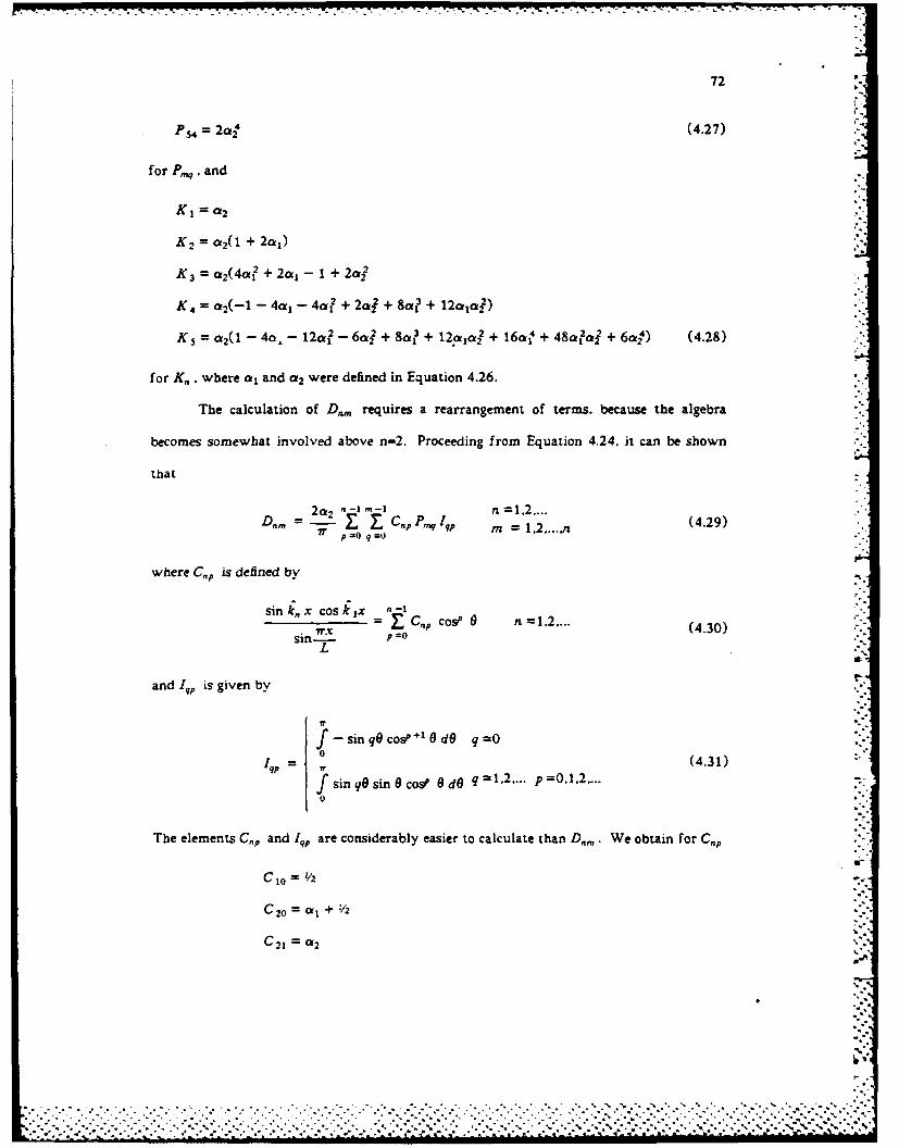
72
P5 = 2a" (4.27)
for P,,. and
K I =a2
K 2 = a 2(1 + 2a 1)
K 3 = a(4a? + 2a, - I + 2ot'
K 4 = a2(-1 - 4a, - 4a2 + 2a2 + 8a 3 + 12aota 2 )
K3 = a21 - 4a. - 12a 2 - 6a2 + 8a3 + 12.fla 2 + 16a 4 + 48at2 + 6a') (4.28)
for K,. where a, and a2 were defined in Equation 4.26.
The calculation of Dm requires a rearrangement of terms, because the algebra
becomes somewhat involved above n-2. Proceeding from Equation 4.24. it can be shown
that
2c 2 -l -- n =1.2....
D.m = p- q0 .'P ~ 9 P m =1.2.....n (4.29)Trp=0 q=O P.'.,Q
where C,, is defined by
sin x cos IX n-1_ = C,, cosP 0 n =1.2.... (4.30)sin w-Ir p =
and Iqp is given by
f sin q9 cosP +10 dO q =001 (4.31)
f sin q sin 0 co9v O dO q .2.... p 0..2....
0
The elements Cp and ,, are considerably easier to calculate than D,,. We obtain for Cnp
CIO = 1/2
C 20 = £k1 + -/Z
C 21 =k
..
, .. ....-. ,•..........,.,...,... ....-. ..---. .. ,-.. -,*.-:-,,., -- ,D,,,.' . ,,,'',
73
C 30 = 1- /z + 2a2
C 31 = 0 2 + 4o10(2
C 32 = 2al
C40 = -- 2 - 2a, + 2a,2 + 4ar1'
C 41 = -2*2 + 4ao1f2 + 12aIa2
C42 = 2a2 + 12a1 ay
C 43 = 4a3
C50 = 1/ - 2a,1 6a,2 + 4a3? + 8a4C 51 = -2 2 - 12ala2 + 12a 2 + 32a3a
Cs 2 = "-6o2 + 12ailaz + 48a2 2
C53 = 4o9 + 32ala3
C 54 = 8 (4.32)
and the values of Iqp are listed in Table 4.1. By using this method of generating D,,,,. we
reduce slightly the efficiency of the program, by introducing a double summation over p
and q. We save. however, a great deal of algebra that would otherwise have to be carried
out by hand. so it seems like a small price to pay.
Now that the singular integral equation technique has been formulated and
extended to the fifth order; we consider some results in the next section.
Table 4.1. Values of Ifp as defined in Equation 4.29.
p1. 0 1 2 3 4q 0 0 -1r/2 0 -3w/8 0
1 7r/2 0 r/8 0 7r/162 0 7r/4 0 #r/8 03 0 0 7r/8 0 3r/324 0 0 0 7r/16 0
.. -
. . . . . .**.. * *.
• .. . , , . .. ... . . . . . .. . .. ... , .-.-.. .. ... . -. ..-...... .-.... ,... . ..-.. : . ,, ., .- ...,-.- .'.,, ,- . .-... -,
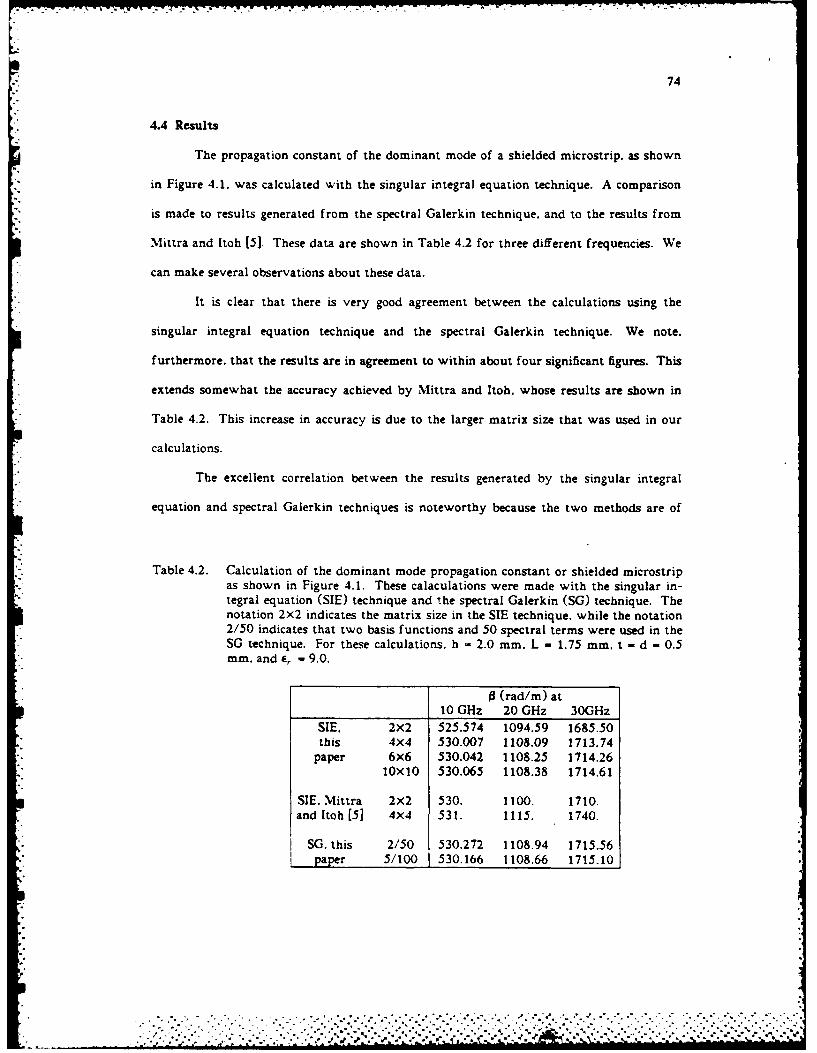
74
4.4 Results
The propagation constant of the dominant mode of a shielded microstrip. as shown
in Figure 4.1. was calculated with the singular integral equation technique. A comparison
is made to results generated from the spectral Galerkin technique, and to the results from
Mittra and Itoh (5]. These data are shown in Table 4.2 for three different frequencies. We
can make several observations about these data.
It is clear that there is very good agreement between the calculations using the
singular integral equation technique and the spectral Galerkin technique. We note.
furthermore, that the results are in agreement to within about four significant figures. This
extends somewhat the accuracy achieved by Mittra and Itoh. whose results are shown in
Table 4.2. This increase in accuracy is due to the larger matrix size that was used in our
calculations.
The excellent correlation between the results generated by the singular integral
equation and spectral Galerkin techniques is noteworthy because the two methods are of
Table 4.2. Calculation of the dominant mode propagation constant or shielded microstripas shown in Figure 4.1. These calaculations were made with the singular in-tegral equation (SIE) technique and the spectral Galerkin (SG) technique. Thenotation 2X2 indicates the matrix size in the SIE technique. while the notation2/50 indicates that two basis functions and 50 spectral terms were used in theSG technique. For these calculations. h - 2.0 mm. L - 1.75 mm. t d - 0.5mm, and e, 9.0.
- (rad/m) at10 GHz 20 GHz 30GHz
SIE. 2x2 525.574 1094.59 1685.50this 4X4 530.007 1108.09 1713.74
paper 6x6 530.042 1108.25 1714.2610xl0 530.065 1108.38 1714.61
SIE. Mittra 2x2 530. 1100. 1710.and toh [5I 4X4 531. 1115. 1740.
SG. this 2/50 530.272 1108.94 1715.56paper 5/100 530.166 1108.66 1715.10
.5... .%. ~
** * * J . ' . ? . ,
. . .
.. ... ,,,,,,., ..-... k L,- -.-- w~i m m k-. V'
. -°

75
very different natures. It was not clear, based on previous work, that the spectral Galerkin
technique could be used to generate the dominant mode propagation constant to such a high
degree of accuracy.
An attempt was made to calculate higher-order evanescent modes with the singular
integral equation technique. This. in theory, is easy to do by changing the propagation
constant from purely- real to purely imaginary. In practice. it turns out that the
determinant function that must go through zero is ill-behaved, and does not have any clear
zeros. Thus, the method doesn't seem to work for evanescent modes. One explanatin for
this result could be that we have only calculated enough matrix elements to fill a lOXlO
matrix. We could, of course. have calculated more elements, but the amount of algebra
required to do so tends to become very large, very fast. This places a practical limit on the
matrix size.
4.5 Conclusion
Although the original goal of the singular integral equation technique. that of
finding higher-order evanescent modes, was not met. we did achieve excellent success in
verifying the propagation constant of the propagating modes. In doing so. we have
demonstrated agreement between two very different methods, the singular integral equation
method and the spectral Galerkin technique. to four significant figures in the final answer.
This degree of accuracy is very high, given the complexity of the calculation and the very
different natures of the two methods used for the comparison.
". . . . . . . . . . . .
',- . . . . . . . . .
Jb '""*"Pw r| . %a l, .lh | 4 % "" . " . """ . .. ."°" % " ' * ' " " " " '" "lm~ lm I~ m l' l ..... '% % " ""'" % " ' * ° ' °- .. m . - •
76
CHAPTER 5
COPULED-MODE ANALYSIS OF MUnLTICONDUCTOR MICROSTRIP LINES
5.1 Introduction
Recent advances in microelectronic packaging have generated a number of difficulties
associated with interconnections between VLSI logic devices. These interconnections are
typically made with large numbers of microstrip lines that run parallel to each other. It is
possible. under certain conditions, that a signal propagating on one line can couple to other
lines. This cross-talk can trigger false signals on nearby lines. Therefore. it is important to
fully analyze multiple microstrip lines, in order to determine the performance of the
overall system. These cross-talk problems become more serious as switching speeds and
packing densities are increased.
Coupled microstrip lines have been analyzed with several different methods
[6.7.50.51]. More recently, multiconductor transmission lines with more than two lines
have received some attention [52,53]. These analyses, however, are all based on a quasi-
static approximation which is valid only for digital devices with switching speeds in the
order of one nanosecond. When the rise time of the switching pulse is reduced to hundreds
of picoseconds. the spectral content of the pulse contains higher-frequency components.
Since quasi-static approximations break down at high frequencies. a full-wave analysis of
multiconductor microstrip transmission lines becomes necessary.
The configuration under study is shown in Figure 5.1. It is composed of five
microstrip lines, each of the same width and strip separation. In this chapter we would like
to demonstrate. using a frequency-dependent analysis, the mechanism whereby current that
is excited on one line is transferred to other lines. We begin with an analysis of the modes
of propagation on the line.
2..
. .. . . . . . . . . . . . . . . .
. . . . . . .
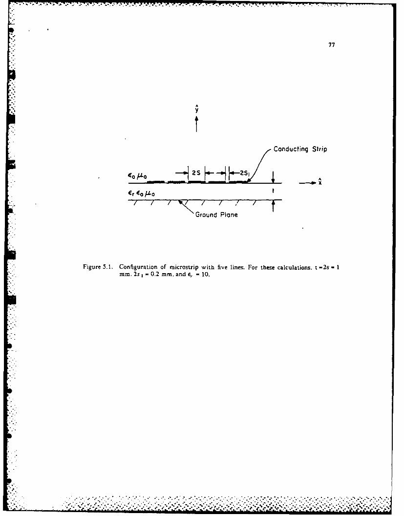
" . . a "--. *- . .
77
Conducting Strip
co .lo -2S 2S- x
er Eo/Jo t": ' I / I , /, I I " / t
Ground Plane
Figure 5.1. Configuration of microstrip with five lines. For these calculations, t -2s - Imm. 2s1 = 0.2 mm. and e, = 10.
%-.................................................
° . . . . . . . . . .-"- * ** .
78
5.2 Calculation of Modes
In a multiple microstrip configuration with N strips, there are N modes of
propagation down these lines. In order to analyze the crosstalk and propagation delay of
these lines, the propagation constant for each of the N propagating modes is needed. The
method we use for this calculation is the spectral Galerkin technique. described in Chapter
2. By making a number of alterations. the same theory can handle multiple lines as well as
a single one.
We begin the analysis with the matrix equation generated by the spectral Galerkin
technique for a single shielded line. This equation was given previously in Equation 2.16.
for the configuration shown in Figure 2.1. In order to remove the top wall, we make a
modification in the spectral Green's function. This is done by replacing the short circuits in
the equivalent transmission lines, at y = h - d. shown in Figure 2.3. with matched loads.
The side walls, on the other hand, are removed by moving them far enough away from the
strips that they have no effect. Care must be taken, however, not to move them too far
away. since the number of spectral terms required for this calculation can become large
with wide side walls.
All that remains now is to generate a reasonable set of basis functions for the
current on the lines. We choose to build our basis functions up from a set of functions that
would be suitable for finding the odd and even modes in a microstrip containing only a
single strip. These building block functions are
(X cos ((i - 1)r(x Is + 1)) (x sin ((i - 1'2)wr(x Is + I))X1 - (x/s 7x "/ - (x/s )2
(X cos(( - z1rr(x /s + 1)) (x sin (i r(x /s + 1))
Vi - x is )2 T -(x s )2
We note that ,, and 71., are the same basis functions used for the even modes in a single
line in Chapter 2. These were given in Equation 2.22 and shown in Figures 2.6 and 2.7.
We now take advantage of the symmetry inherent in the structure to find basis
. . .i
. ... . . . .... .. ., . .. _. ......_, , ..
- 79
functions that are either even in J, and odd in J . or odd in J, and even in J.. Although
the method that follows is general for N lines, we show as an example the basis functions
used for five lines as
'-'.N: S
(X C' =li (X
J, (x) = d Qj (x) (5.2)~j =Ii =1
where, for even J2 and odd J.
Pli (x) = , (x) Q ii (X).i (X
P2 (x) = , (x + q) + ,, (x - q) Q2i (x) = i, (X + q) + 7o.(x - q)i" s,3,(X) =& ,(X +q)-fo,(X -q) O.3,(x)=T),,(x +q)-n,,(x -q)
P.Jx)= ,i(x +2q)+&(x -2q) Q 4o(x)='ro,(X +2q)+7o,(x-2q)
"-* P5j(x)=6,(x +2q)-f.,(x -2q) Q 5,(x)-r (x + 2q)-n,,(x-2q) (5.3a)
and for odd J, and even J.,.
P1, (x ) = 6o, (X ) Q1, (x ) " ,(x)
P2,(X)= ,,(X +q)-,,(x -q) Q, (x)i= 0 o,(x +q)-o 1 (x -q)
.P3,(x)=&o,(x +q)+fo,(x -q) Q3i (X)r(X + q)+ l(x - q
".-P4,(x)=f,,(x + 2q)-fi,,(x -2q) Q., (x ).O, (x + 2q)-T ,(Ux- 2q)
P5,(x)=6o,(x +2q)+fo(x-2q) Q,(x)n,(x + 2q)+ 7,(x-2q) (5.3b)
where
q =2(s +s 1 ) (5.4)
With these basis functions, we now search for the three even-mode and two odd-mode
propagation constants that satisfy Equation 2.16. Results showing dispersion curves and
comparisons to the quasi-static theory are presented in Section 5.4.
lo.. . . . . . . . . . ... . . ..
• ~~~~~~~~~~~~~~~~~~~~~~~~. . ....-..........---..-....-...-.-...---..-<.-. .... -,>-?-;--/-' ...................-.-
80
Let us now turn to the coupled mode theory used to explain the transfer of current
between lines.
5.3 Coupled-mode Theory
When a single line of an N-line system is excited, one may consider this to be an
excitation of a linear combination of the five modes, whose weighting coefficients must be
determined. We may consider the integral of J over an individual strip to be the quantity
that is coupled between the lines. Therefore, we carry out a procedure similar to that
described by Bhartia and Bahl [54] for image guide couplers. For each mode. we find the
longitudinal current on strip i due to mode j as
I, = f J (x)dx i.j 1.....5 (5.5)strip t
We consider an excitation of the first line alone to be one where the first line has a
magnitude of one and the others have a magnitude of zero at z - 0. Therefore, we set up a
fifth-order linear equation to find the combination of modes that satisfies the condition
aj, 0 0 i=2 (5.6)ji =
where the a, 's are the unknown mode coefficients.
Once the mode coefficients are determined, we may assume they propagate down the
five-line system, with their respective propagation constants and mode coefficients that were
calculated in the previous section. Thus.
5l
I(z a, I,, e (5.7)'11
where 0, is the propagation constant of the j' mode, and l,'(z ) is the current on the i'6
strip due to all j modes, at a distance z from the original excitation. This can be calculated
iii " . .. . .. . ,..- . .....-.... .. ,..,--..........-., . .,....-..-....,.,...... '... . , ... ,". ..- , d - . a ~ * ~ ~ - " % .' ~ .... . • " " .% ' .* * . " °o "
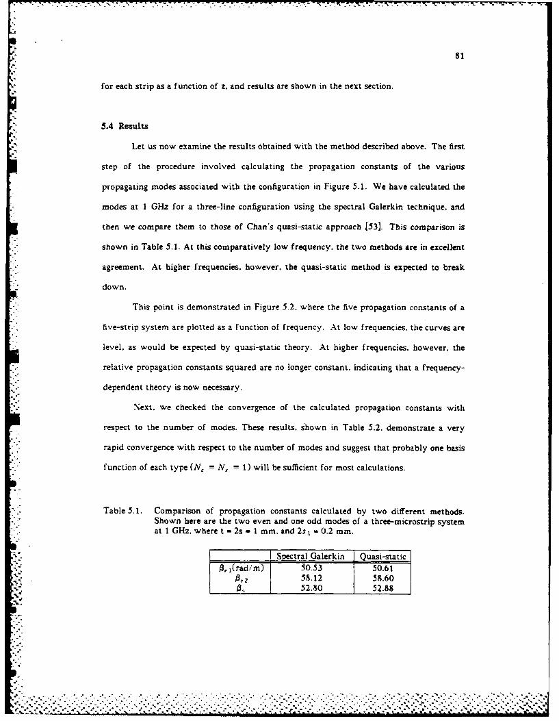
81
for each strip as a function of z. and results are shown in the next section.
5.4 Results
Let us now examine the results obtained with the method described above. The first
step of the procedure involved calculating the propagation constants of the various
propagating modes associated with the configuration in Figure 5.1. We have calculated the
modes at I GHz for a three-line configuration using the spectral Galerkin technique, and
then we compare them to those of Chan's quasi-static approach [53]. This comparison is
shown in Table 5.1. At this comparatively low frequency. the two methods are in excellent
agreement. At higher frequencies. however, the quasi-static method is expected to break
down.
This point is demonstrated in Figure 5.2. where the five propagation constants of a
five-strip system are plotted as a function of frequency. At low frequencies. the curves are
level, as would be expected by quasi-static theory. At higher frequencies. however, the
relative propagation constants squared are no longer constant. indicating that a frequency-
dependent theory is now necessary.
Next. we checked the convergence of the calculated propagation constants with
respect to the number of modes. These results. shown in Table 5.2. demonstrate a very
rapid convergence with respect to the number of modes and suggest that probably one basis
function of each type (N, = N, = 1) will be sufficient for most calculations.
Table 5.1. Comparison of propagation constants calculated by two different methods.Shown here are the two even and one odd modes of a three-microstrip systemat 1 GHz. where t - 2s - 1 mm. and 2s = 0.2 mm.
SSpectral Galerkin Quasi-static
,, 1(rad/m) 50.53 50.610,2 58.12 58.60
52.80 52.88
.. . . . ............ ,. .. . . . . ....... . . . .. . . .. . . . . . . . . . . . . . . . . ..o~N
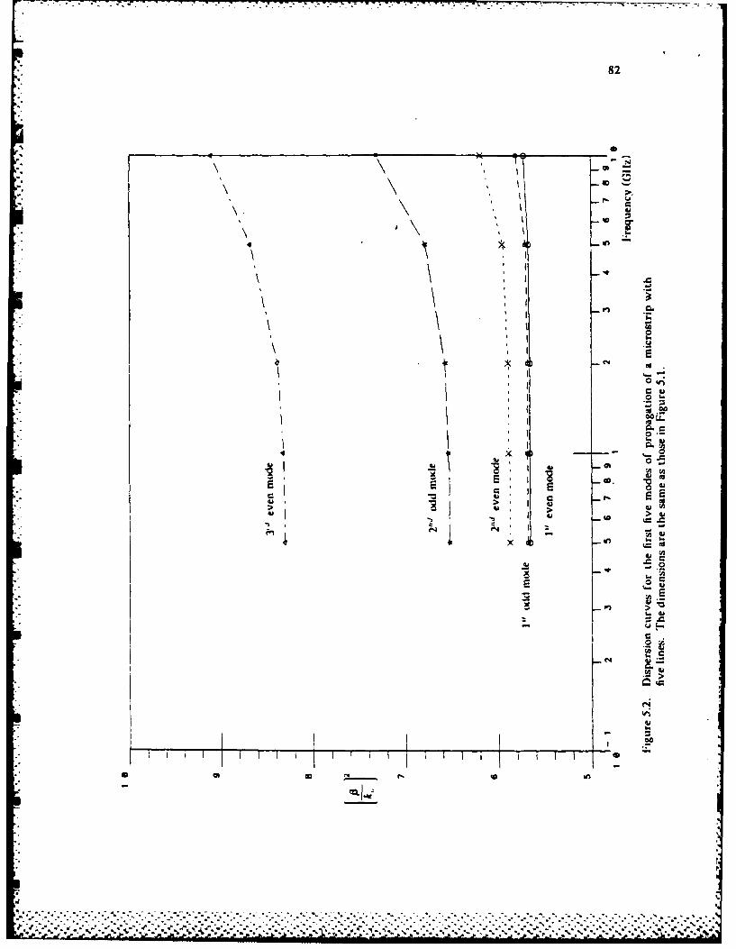
82
(40
C4~
4 x
41
-~~L -3).>
fq I -
cox
4W Q5.
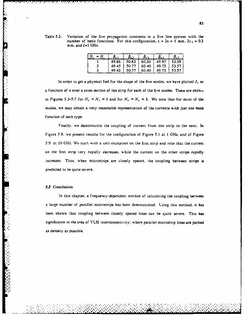
83
Table 5.2. Variation of the five propagation constants in a five line system with thenumber of basis functions. For this configuration. t - 2s = I mm. 2s I = 0.2mm. and f-I GHz.
,'." N.. = N, J3.1o /3 o _
1 49.86 50.83 60.50 49.97 53.582 49.45 50.77 60.40 49.75 53.573 49.42 50.77 60.40 49.73 53.57
In order to get a physical feel for the shape of the five modes, we have plotted J, as
a function of x over a cross section of the strip for each of the five modes. These are shown
in Figures 5.3-5.7 for N, =-N, = 1 and for N. =N, = 3. We note that for most of the
modes, we may obtain a very reasonable representation of the currents with just one basis
function of each type.
Finally. we demonstrate the coupling of current from one strip to the next. In
Figure 5.8. we present results for the configuration of Figure 5.1 at 1 GHz. and of Figure
5.9 at 10 GHz. We start with a unit excitation on the first strip and note that the current
on the first strip very rapidly decreases, while the current on the other strips rapidly
increases. Thus. when microstrips are closely spaced. the coupling between strips is
predicted to be quite severe.
5.5 Conclusion
In this chapter, a frequency-dependent method of calculating the coupling between
a large number of parallel microstrips has been demonstrated. Using this method, it has
been shown that coupling between closely spaced lines can be quite severe. This has
significance in the area of VLSI interconnectivity. where parallel microstrip lines are packed
as densely as possible.
. . .. . . . . .
~~~~~. .. . . . ...................... ,.. ".,', .: . i'-'-,"
=:' ,......... .. .
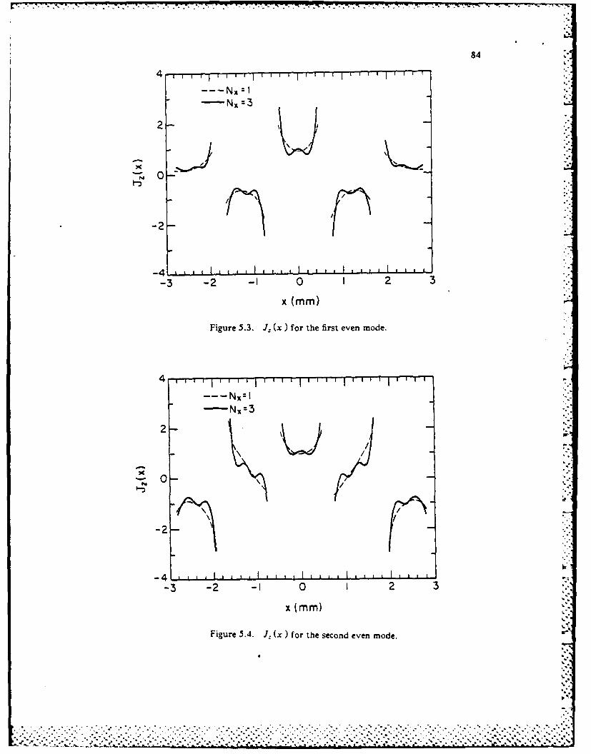
78
48
2-
0/
-2
-2 I In
-3 -2 -i0 I2 3
x (MM)
Figure 5.3. J, (x) for the first even mode.
2-
-
-2-
-3 - I0 I2 3
x (MM)
Figure 5.4. J, (x) for the second even mode.
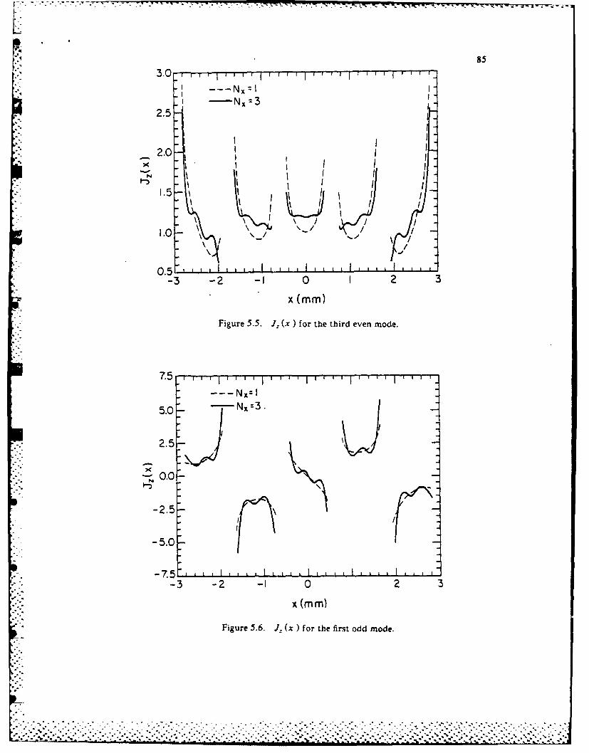
- -. -w~
2.5
2. 1'
2.0
x (M)
7.5 I
-2.5
-3 -2 0Ia 2 3
Figure 5.5. J, (x )for the firdteven mode.
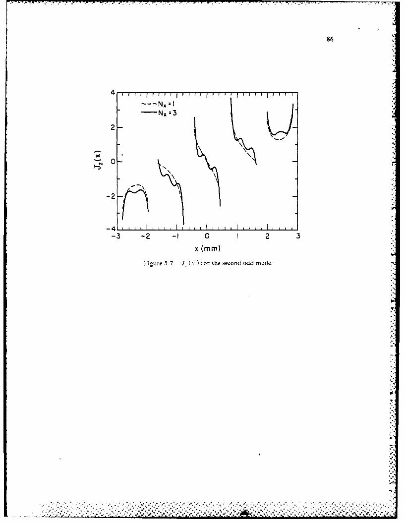
86
-4L,
x (mm)
Figure 5.7. 1. Wx for t~he second odd mode.
. \ \ .. -..
. . . . . .. . . ""
. . . . . . . . . .. . .
. . . . . . . . . .
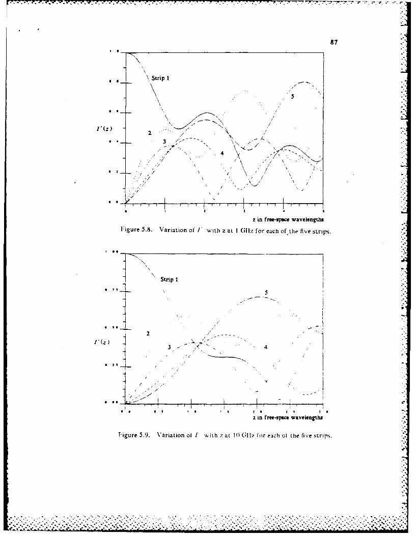
87
\,Strip I
3 -- 6 - - - -
\ *\
. . \
4
... ." ---- \
,/ / ,, .
j '
.', ', I 2 ,, '.
z m free-space wavelengthsFigure 5.8. Variation of f with z at I GIlz for each of the five strips.
Strip I .l '
20
3 -
• ' L .I . ./
I. iO O * j 4 5 2 5 1 5 ,0
z in free-spac wavelengths
Figure 5.9. Variation ol / with z at 10 G11z for each of the five strips.
.. - .. -- - " .o - °- - -. %.. , . . .. . .. - . ° , . . . . . .- ,. . . ,. . . .. * - . . - ,
, %'°-.* °-° '.-'% ,' . '.,''1 .''- %°"° "%"%'°"° "." *°- * ', ". ."
"'" -'° " ' " " °-'°* ."' ° ". '.- ' . . *'. ' ." • . *t '
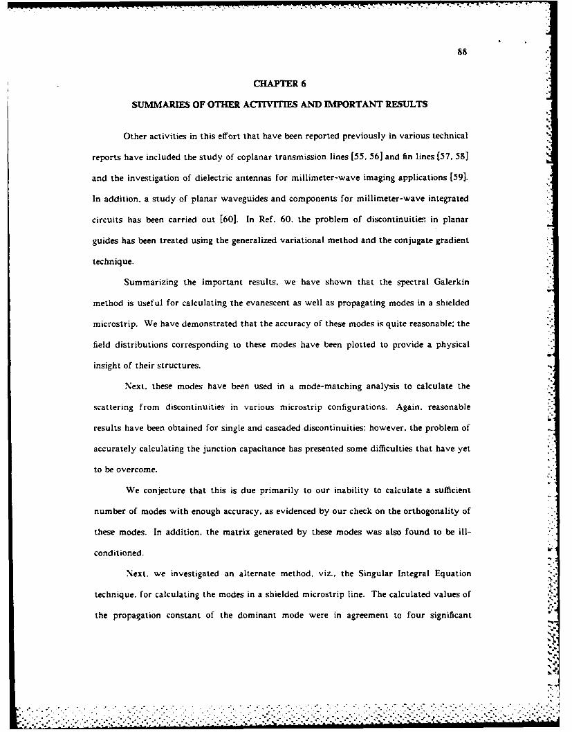
88
CHAPTER 6
SUMMARIES OF OTHER ACTIVITIES AND IMPORTANT RESULTS
Other activities in this effort that have been reported previously in various technical
reports have included the study of coplanar transmission lines [55. 561 and fin lines [57. 581
and the investigation of dielectric antennas for millimeter-wave imaging applications [591.
In addition, a study of planar waveguides and components for millimeter-wave integrated
circuits has been carried out [601. In Ref. 60, the problem of discontinuities in planar
guides has been treated using the generalized variational method and the conjugate gradient
technique.
Summarizing the important results, we have shown that the spectral Galerkin
method is useful for calculating the evanescent as well as propagating modes in a shielded
microstrip. We have demonstrated that the accuracy of these modes is quite reasonable: the
field distributions corresponding to these modes have been plotted to provide a physical
insight of their structures.
Next, these modes have been used in a mode-matching analysis to calculate the
scattering from discontinuities in various microstrip configurations. Again, reasonable
results have been obtained for single and cascaded discontinuities; however, the problem of
accurately calculating the junction capacitance has presented some difficulties that have yet
to be overcome.
We conjecture that this is due primarily to our inability to calculate a sufficient
number of modes with enough accuracy, as evidenced by our check on the orthogonality of
these modes. In addition, the matrix generated by these modes was also found to be ill-
conditioned.
Next, we investigated an alternate method, viz., the Singular Integral Equation8,
technique, for calculating the modes in a shielded microstrip line. The calculated values of
the propagation constant of the dominant mode were in agreement to four significant
.1,
.... -......-.... .....................-... :...-. -......... , .............. ,..- .:-::,,.
% .R .. • " . .° -o -. . - =. . - - . . - -" " - " . . . . . . . . - . .
89
figures. with results generated with the spectral Galerkin technique. This degree of
accuracy is exceptional. because the two methods that are being compared are quite
different. An attempt was made to calculate evanescent modes using the singular integral
equation technique. but these modes were not found. One possible explanation was that the
size of the matrix we could use was too small. Using a larger matrix was not practical
because the complexity of the matrix elements increases rapidly with matrix size.
The generalized variational method and the conjugate gradient method, both of
which are iterative techniques, have been employed to derive the solution to the
discontinuity problems in planar guides, but they have also yielded only limited success in
terms of the realized accuracy of the results. Thus, our conclusion is that further effort in
this direction is critically needed.
Finally. the dielectric antenna we have developed has been demonstrated to be
useful as an array element of an imaging system at 80 Gliz and 220 Gllz. Again, a
monolithic imaging system would be better suited for this purpose and it would be
worthwhile, in the future, to investigate such a monolithic system.
% S,
--| • -I- - . . . . .-... . r r•
90
LIST OF PUBLICATIONS AND TECHNICAL REPORTS
Publications
1. Y. Hayashi and R. Mittra. "An analytical investigation of finlines with magnetized
ferrite substrate." IEEE Trans. Microwave Theory Tech., vol. MTT-31. no. 67, pp. 495-
498. June 1983.
2. N. Deo and R. 'littra, "A technique for analyzing planar dielectric waveguides for
millimeter wave integrated circuits." AEU. Band 37. Heft 7/8. July/Aug. 1983. pp.
236-244.
3. K. Webb and R. Mittra. "Dielectric waveguide grating filter." AEU, Band 38, Heft 1. pp.
51-54. Jan./Feb.. 1984.
4. T. Kitazawa and R. Mittra. "An investigation of striplines and fin lines with periodic
stubs." IEEE Trans. Microwave Theory Tech.. vol. MTT-32. no. 7. pp. 684-688. July
1984.
5. T. Kitazawa and R. Mittra, "Analysis of finline with finite metallizatior, thickness," IEEE
Trans. Microwave Theory Tech., vol. MTT-32. no. 11. pp. 1484-1487. November 1984.
6. E. Farr. K. Webb and R. Mittra. "Studies in fin-line antenna design for imaging array
applications, AFU, Band 39, Heft 2. pp. 87-89, March/April 1985.
7. T. Kitazawa and R. Mittra. "Analysis of Asymmetric Coupled Striplines." IEEE Trans.
Microwave Theory Tech., vol. MTT-33, no. 7, pp. 643-646, July 1985.
8. T. Kitazawa and R. Mittra. "Quasi-static characteristics of asymmetrical and coupled
coplanar-type transmission lines," IEEE Trans. Microwave Theory Tech., vol. MTT-33,
no. 9, pp. 771-778, September 1985.
9. K. J. Webb and R. Mittra. "A variational solution of the fin-line discontinuity problem."
Proceedings o/ the 15th European Microwave Conference. September 1985.
......... .. . .. . . . . . .
~A-il444 NILLINETER-NAVE INTEGRATED CIRCUITSCU ILLINOIS UNIY AT jj22
URBANA ELECTROMAGNETIC COMUNICATION LAS R MITTRA
I UNCLASSIFIED F/G 9/5 Ht7 EEEEEE
1111.0 1211111 Li
LI
1111 5 1 .4 =61.
MICROCOPY RESOLUTIO1N TEST CHART
LZ L
4 7 f
91 h
10. K. Webb. E. Farr and R. Mittra, "A note on the numerical solution for finline and
microstrip modes." to be published in IEEE Trans. Microwave Theory Tech.
11. E. Farr. C. Chan and R. Mittra. "A frequency-dependent coupled-mode analysis of
multiconductor microstrip lines with application to VLSI interconnection problems." to
be published in IEEE Trans. Microwave Theory Tech.
12. K. Webb and R. Mittra. "Solution of the fin-line discontinuity problem using the
generalized variational technique." to be published in IEEE Trans. Microwave Theory
Tech.
Technical Reports
1. Y. Havashi and R. Mittra. "An analytical investigation of fin lines with magnetized
ferrite substrate." EM Lab Report 82-4. University of Illinois. June 1982.
2. J. S. Wilson and R. Mittra. "Analysis of fin-line at millimeter wavelengths." EM Lab
Report 82-6. University of Illinois. July 1982.
3. Y. Hayashi. E. Farr and R. Mittra. "Analysis of dominant and higher-order modes in
unilateral fin lines." EM Lab Report 82-9. University of Illinois. August 1982.
4. K. Webb and R. Mittra. "Dielectric waveguide grating filter." EM Lab Report 82-11.
University of Illinois. November 1982.
5. T. N. Trinh and R. Mittra. "Analysis of the suspended Ht-waveguide and other related
dielectric waveguide structures," EM Lab Repot 83-1. University of Illinois. January
1983.
6. T. Kitazawa and R. Mittra. "Analysis of fin-lines with the finite metallization thickness."
EM Lab Report 83-11. University of Illinois. October 1983.
7. T. Kitazawa and R. Mittra. "An investigation of strip lines and fin lines with periodic
stubs." EM Lab Report 83-13, University of Illinois. October 1983. "
8. E. Farr, K. Webb and R. Mittra. "Studies in fin-line antenna design for phased array
applications." EM Lab Report 83-14. University of Illinois. November 1983.
.
%
%* :TSYO . .4.--. .. 4VS6, it
92
9. T. Kitazawa and R. Mittra. "Asymmetrical coplanar transmission lines." EM Lab Report
84-9. University of Illinois. June 1984.
10. K. Webb and R. Mittra. "Investigation of planar waveguides and components for 4.
rI
millimeter-wave integrated circuits," EM Lab Report 84-3. University of Illinois.
October 1984.
11. S. H. Doran and R. Mittra. "An experimental study of dielectric rod antennas for
millimeter-wave imaging applications." EMC Lab Report 85-3. University of Illinois.
March 1985.
12. T. Kitazawa and R. Mittra. "Quasistatic characteristics of asymmetrical and coupled
coplanar-type transmission lines." EMC Lab Report 85-4. University of Illinois. April
1985.
V.
b-
°1
! -"
.4"4
r . J'.a' 'P d'''' '.,.* , ' '. .. , . d . , .. '., ,r ." .'.,"..." € " -" ." .. .' ." " '..,- a' .' . -. ." ."• "b•
" .5/'
4".
93
SCIENTIFIC PERSONNEL AND DEGREES AWARDED
Scientific Personnel
Professor Raj Mittra, Principal Investigator
Visiting Scholars
Dr. Y. HayashiDr. T. KitazawaDr. Z. Pantic
Research Students
Mr. Sunil BhooshanMr. Chi ChanMr. Albert ChangMr. Sean DoranMr. Everett FarrMr. Ben HalpernMr. Charles SmithMr. Trang TrinhMr. Kevin WebbMr. Scott Wilson
Theses
I. "Analysis of fin-line at millimeter wavelengths." M.S. thesis. John S. Wilson. May 1982.
2. "Analysis of the suspended li-waveguide and other related dielectric waveguidestructures." Ph.D. thesis. Trang N. Trinh. December 1982.
3. "Investigation of planar waveguides and components for millimeter-wave integratedcircuits." Ph.D. thesis. Kevin J. Webb. August 1984.
4. "A novel technique for the analysis of dielectric waveguides." Ph.D. thesis. Sunil V.Bhooshan. January 1985.
5. "Analysis of microstrip discontinuities using the finite element method." M.S. thesis.Albert H. Chang. January 1985.
6. "An experimental study of dielectric rod antennas for millimeter-wave imagingapplications." M.S. thesis. Sean H. Doran. January 1985.
7. "An investigation of modal characteristics and discontinuities in printed circuit- transmission lines," Ph.D. thesis, Everett G. Farr. August 1985.
'.%
a
* . - ..°, * . . . . . . . . . .
4.. 4. ' 4~°' 4 ~ ~ *
94
REFERENCES
[1] T. Itoh and R. Mittra. "Spectral domain approach for calculating the dispersioncharacteristics of microstrip lines," IEEE Trans. Microwave Theory Tech., vol.MTT-19. pp. 30-39. Jan. 1971.
[2] T. Itoh and R. Mittra. *A technique for computing dispersion characteristics ofshielded microstrip lines." 1EEE Trans. Microwave Theory Tech., vol. MTT-22. pp.896-898, Oct. 1974.
[3] R. Mittra and S.W. Lee. Analytical Techniques in the Theory of Guided Waves. NewYork: Macmillan. 1971.
[4] A. Wexler. "Solution of waveguide discontinuities by modal analysis." IEEE Trans.Microwave Theory Tech., vol. MTT-15. pp. 508-517. Sept. 1967.
[5] R. Mittra and T. Itoh, "A new technique for the analysis of the dispersioncharacteristics of microstrip lines." IEEE Trans. Microwave Theory Tech.. vol.MTT-19, pp. 47-56. Jan. 1971.
[6] il.A. Wheeler. "Transmission line properties of parallel strips separated by a
dielectric sheet." IEEE Trans. Microwave Theory Tech.. vol. MTT-13. pp. 172-175.Mar. 1965.
[7] T.G. Bryant and J.A. Weiss, "Parameters of microstrip transmission lines and ofcoupled pairs of microstrip lines." IEEE Trans. Microwave Theory Tech., vol. MTT-16. pp. 1021-1027. Dec. 1968.
[8] R.D. Ward. "Application of Galerkin's Method for Analyzing MicrostripTransmission Line." M.S. Thesis. University of Illinois at Urbana-Champaign. 1971.
[9] Y. Rahmat-Samii. "Application of Fourier and Galerkin Techniques for AnalyzingDiscontinuities and Coupling Phenomena in Microstrip Lines." M.S. Thesis.University of Illinois at Urbana-Champaign. 1972.
[10] E. Yamashita and K. Atsuki. "Analysis of microstrip-like transmission lines bynonuniform discretization of integral equations." IEEE Trans. Microwave TheoryTech., vol. MTT-24. pp. 194-200, Apr. 1976.
[111 A.-M. A. El Sherbiny. "Exact analysis of shielded microstrip lines and bilateral fin-lines." IEEE Trans. Microwave Theory Tech.. vol. MTT-29, pp. 669-675. July 1981.
4 [12] D. Mirshekar-Syahkal and J. Brian Davies. "Accurate solution of microstrip and% coplanar structures for dispersion and for dielectric and conductor losses," IEEE
Trans. Microwave Theory Tech., vol. MTT-27. pp. 694-699. July 1979.
a.-.- "-- %% .. ° -
..'''' -." " •. ."- " ..- S.-.... .........- °" %•"
%. ZW, NNE.-
- .
95
[13] T. Itoh. "Spectral domain immitance approach for dispersion characteristics ofgeneralized printed transmission lines." IEEE Trans. Microwave Theory Tech., vol.MTT-28. pp. 733-736. July 1980.
[14] J.B. Knoor and P.M. Shayda. "Millimeter-wave fin-line characteristics," IEEE Trans.Microwave Theory Tech., vol. NITT-28. pp. 737-743. July 1980.
[15] L.P. Schmidt and T. Itoh. "Spectral domain analysis of dominant and higher-ordermodes in fin-lines." IEEE Trans. Microwave Theory Tech., vol. MTT-28. pp. 981-985.Sept. 1980.
[161 L.P. Schmidt. T. ltoh. and H1. lofmann. "Characteristics of unilateral fin-linestructures with arbitrarily located slots." IEEE Trans. Microwave Theory Tech., vol.MTT-29. pp. 352-355. Apr. 1981.
[17] M. Helard et al.. "Exact calculations of scattering parameters of a step slot widthdiscontinuity in a unilateral fin-line." Electron. Left.. vol. 19. pp. 537-539. July 7.1983.
[18] R.F. Harrington. Time Harmonic Electromagnetic Fields. New York: McGraw Hill.1961. pp. 129-132.
[19] H. Bateman. Tables of Integral Transforms vol. 1. New York: McGraw Hill. 1954. p.139.
[20] F. Arndt and G.V. Paul. "The reflection definition of the characteristic impedance ofmicrostrips." IEEE Trans. Microwave Theory Tech., vol. MTT-27. pp. 724-731. Aug.1979.
[211 R.l. Jansen. "Unified user-oriented computation of shielded, covered, and openplanar microwave and millimeter-wave transmission-line characteristics." IEEEProc. I. HI. Microwaves Opt. Acoust.. vol. MOA-1. pp. 14-22. Jan. 1979.
[22] B. Bianco et al.. "Some considerations about the frequency dependence of uniformmicrostrips." IEEE Trans. Microwave Theory Tech., vol. MTT-26. pp. 182-185. Mar.1978.
[231 W.J. Getsinger. "Microstrip characteristic impedance," IEEE Trans. MicrowaveTheory Tech., vol. MTT-27. p. 293. Apr. 1979.
[24] R.F. Harrington. Time Harmonic Electromagnetic Fields. New York: McGraw Hill.1960. pp. 458-459.
[25] P.E. Mayes. Electromagnetics for Engineers. Ann Arbor: Edwards Bros.. 1965. pp.63-65.
....... ........ ..... ........... ...... ............
96
[26] D.W. Dearholt and W.R. McSpadden. Electromagnetic Wave Propagation. NewYork: McGraw Hill. 1973, p. 151.
[271 A. Farrar and A.T. Adams. "Matrix methods for microstrip three-dimensionalproblems," IEEE Trans. Microwave Theory Tech., vol. MTT-20. pp. 497-504. Aug.1982.
[281 P. Benedek and P. Silvester. "Equivalent capacitances for microstrip gaps and steps.*IEEE Trans. Microwave Theory Tech., vol. MTT-20. pp. 729-733. Nov. 1972.
[291 R. Horton. "Equivalent representation of an abrupt impedance step in microstripline." IEEE Trans. Microwave Theory Tech., vol. MTT-21. pp. 562-564. Aug. 1973.
[30] A. Gopinath. A.F. Thompson. and I.M. Stephenson. "Equivalent circuit parametersof microstrip step change in width and cross junctions." IEEE Trans. MicrowaveTheory Tech.. vol. MTT-24. pp. 144. March 1976.
[31] 1. Wolf. G. Kompa, and R. Mehran. "Calculation method for microstripdiscontinuities and T-junctions." Electron. Lett.. vol. 8. pp. 177-179. April 1972.
[32] G. Kompa. "S-matrix computation of microstrip discontinuities with a planarwaveguide model." Arch. Elek. Ubertragung., vol. 30, pp. 58-64, 1975.
[33] W. Menzel and 1. Wolff. "A method for calculating the frequency-dependentproperties of microstrip discontinuities." IEEE Trans. Microwave Theory Tech., vol.MTT-25. pp. 107-112. Feb. 1977.
[34] Y.C. Shih. T.S. Chu. and T. Itoh. "Comparative study of mode matchingformulations for microstrip discontinuities." IEEE MTT-S International MicrowaveSymposium Digest, pp. 435-438. June 1985.
[351 R. Lampe. "Discontinuities in Suspended Substrate Strip Transmission Lines." Ph.D.Thesis. University of Illinois at Urbana-Champaign. 1983.
[361 H. El Hennawy and K. Schunemann. "Impedance transformation in fin-lines." IEEEProc. Pr. H, Microwaves, Opt. Acoust., vol. 129. pp. 342-350. Dec. 1982.
[371 H. El Hennawy and K. Schunemann, "Hybrid fin-line matching structures" IEEETrans. Microwave Theory Tech., vol. MTT-30. pp. 2132-2139. Dec. 1982.
[38] K. Webb, "Investigation of Planar Waveguides and Components for MillimeterWave Applications." Ph.D. Thesis. University of Illinois at Urbana-Champaign.1984.
[39] R.E. Collin. Field Theory of Guided Waves New York: McGraw Hill. 1960. pp.174-179.
o79
%-• -..... . - . .. - - . - - ... . - . . . . - .- . . .. -.. . . - .. . .- .. .., -,,- ., . -, -.., . ..,, .. . . -. -. - ., - ; ." .-. -.*
*6~ 97
[401 C.A. Klein and R. Mittra. "Stability of matrix equations arising in electromagnetics."IEEE Trans. Antennas Propa gat., vol. AP-21. pp. 902-905. Nov. 1973.
[41] R. Mittra. ed.. Numerical and Aiynzpotic Techniquesi in Electromagnetics. Berlin:Springer-Verlag. 1975. pp. 129-134.
[42] R. Hall. Ph.D. Thesis. University of Illinois at Urbana-Champaign. (to bepublished).
[431 U. Feldman. "Characterization of Microstrip Discontinuities in the Time andFrequency Domains.! M.S. Thesis. University of Illinois. 1985, p. 40.
[44] A.S. Omar and K. Schune-.ann. "Space-domain decoupling of LSE and LSM fields ingeneralized planar guiding structures." IEEE Trans. Microwave Theory Tech., vol.M1'T-32. pp. 1626-1632. Dec. 1984.
[45] A.S. Omar and K. Schunemann. "Formulation of the singular integral equationtechnique for general planar transmission lines.* IEEE M77'-S InternationalMicrowave Symposium Digest, pp. 135-138. June 1985.
[46] L. Lewin. Advanced Theory of Waveguides. London: Iliffe. 1951.
[47] L. Lewin, "The use of singular integral equations in the solution of waveguideproblems." in Advances in Microwaves, vol. 1. L. Young. Ed. New York: AcademicPress. 1966. pp. 212-284.
[48] L. Lewin, Theory of Waveguides. New York: Wiley. 1975.
[49] F.G. Tricomi. Integral Equations. New York- lnterscience. 1957. pp. 161-217.
[501 F. Yamashita and R. Mittra. "Variational method for the analysis of m icrostriplines." IEEE Trans. Microwave Theory Tech.. Vol. MTT-16. pp. 251-256. Apr. 1968.
[51] Y. Rahmat-Samii. T. Itoh, and R. Mittra. "A spectral domain technique for solvingcoupled microstrip line problems." Archiv. fur Elek. Ubertragung.. Vol. 27. pp. 69-71. Feb. 1973.
[521 Cao Wei et al.. "Multiconductor transmission lines in multilayered dielectric media."JEEE Trans. Microwave Theory Tech., Vol. MTT-32. pp. 439-449. Apr. 1984.
[53] C. Chan and R. Mittra. "Spectral iterative techniques for analyzing multiconductormicrostrip lines." IEEE M77' Symposium Digest. pp. 463-465. May 1984.
[541 P. Bhartia and 1. J. Bahl. Millimeter Wave Engineering and Applications. New York:Wiley. 1984. pp. 379-380.
-... "-....... ..
V% .1 '6.r;.:. %.'.*...~- ~ ~ t*~** ~ ~ ~ * . . . * *
.7 . .7 N*
98
[55] T. Kitazawa and R. Mittra. "Asymmetrical coplanar transmission lines." EM LabReport No. 84-9. University of Illinois. June 1984
(561 T. Kitazawa and R. Mittra. "Quasistatic characteristics of asymmetrical and coupledcoplanar-type transmission lines." EN Lab Report No. 85-4, University of Illinois.April 1985.
[57] T. Kitazawa and R. Mittra. "Analysis of fin-lines with the finite metallizationthickness." EM Lab Report No. 83-11. University of Illinois. October 1983.
(581 T. Kitazawa and R. Mittra, "An investigation of strip lines and fin lines withperiodic stubs." EM Lab Report No. 83-13. University of Illinois. October 1983.
159) S. H. Doran and R. Mittra. "An experimental study of dielectric rod antennas formillimeter-wave imaging applications." EMC Lab Report No. 85-3. University ofIllinois. March 1985.
(601 K. J. Webb and R. Mittra. "Investigation of planar waveguides and components formillimeter-wave integrated circuits." EMC Lab Report No. 84-3, University ofIllinois. October 1984.
.A .......................................
.5 ... .. .. * . . . . - . . .* %
5o.* * *~~ * S S~* *S * ~ * * . * SS
-. ~~~ . .. .. . . 77
-~- -
bdw
FILMED,' 1-86iIse
°;',2DTIC
.. . ...-. ,~
~ .' ' ... . .*t * .-