Embed Size (px)
Citation preview

4-Mbit (128K x 32) Pipelined Sync SRAM
CY7C1339G
Cypress Semiconductor Corporation • 198 Champion Court • San Jose, CA 95134-1709 • 408-943-2600Document #: 38-05520 Rev. *F Revised July 5, 2006
Features• Registered inputs and outputs for pipelined operation• 128K × 32 common I/O architecture • 3.3V core power supply (VDD)• 2.5V/3.3V I/O power supply (VDDQ)• Fast clock-to-output times
— 2.6 ns (for 250-MHz device)• Provide high-performance 3-1-1-1 access rate• User-selectable burst counter supporting Intel®
Pentium® interleaved or linear burst sequences• Separate processor and controller address strobes• Synchronous self-timed writes• Asynchronous output enable• Available in lead-free 100-Pin TQFP package, lead-free
and non-lead-free 119-Ball BGA package• “ZZ” Sleep Mode Option
Functional Description[1]
The CY7C1339G SRAM integrates 128K x 32 SRAM cells withadvanced synchronous peripheral circuitry and a two-bitcounter for internal burst operation. All synchronous inputs aregated by registers controlled by a positive-edge-triggeredClock Input (CLK). The synchronous inputs include alladdresses, all data inputs, address-pipelining Chip Enable(CE1), depth-expansion Chip Enables (CE2 and CE3), BurstControl inputs (ADSC, ADSP, and ADV), Write Enables(BW[A:D], and BWE), and Global Write (GW). Asynchronousinputs include the Output Enable (OE) and the ZZ pin.Addresses and chip enables are registered at rising edge ofclock when either Address Strobe Processor (ADSP) orAddress Strobe Controller (ADSC) are active. Subsequentburst addresses can be internally generated as controlled bythe Advance pin (ADV).Address, data inputs, and write controls are registered on-chipto initiate a self-timed Write cycle.This part supports Byte Writeoperations (see Pin Descriptions and Truth Table for furtherdetails). Write cycles can be one to four bytes wide ascontrolled by the byte write control inputs. GW when activeLOW causes all bytes to be written. The CY7C1339G operates from a +3.3V core power supplywhile all outputs may operate with either a +2.5 or +3.3Vsupply. All inputs and outputs are JEDEC-standardJESD8-5-compatible.
1
Note: 1. For best-practices recommendations, please refer to the Cypress application note System Design Guidelines on www.cypress.com.
A DDRESSREGISTER
A DVCLK BURST
COUNTERA ND
LOGICCLR
Q1
Q0
A DSP
A DSC
M ODE
BW E
GWCE1
CE2
CE3
OE
ENA BLEREGISTER
OUTPUTREGISTERS
SENSEA M PS
OUTPUTBUFFERS
E
PIPELINEDENA BLE
INPUTREGISTERS
A 0, A 1, A
BW B
BW C
BW D
BW A
M EM ORYA RRA Y
D Q s
SLEEPCONTROL
ZZ
A [1:0]2
DQ A
BY TEW RITE REGISTER
DQ B
BY TEW RITE REGISTER
DQ C
BY TEW RITE REGISTER
DQ D
BY TEW RITE REGISTER
DQ A
BY TEW RITE DRIV ER
DQ B
BY TEW RITE DRIV ER
DQ C
BY TEW RITE DRIV ER
DQ D
BY TEW RITE DRIV ER
Logic Block Diagram
[+] Feedback
CY7C1339G
Document #: 38-05520 Rev. *F Page 2 of 18
Pin Configurations
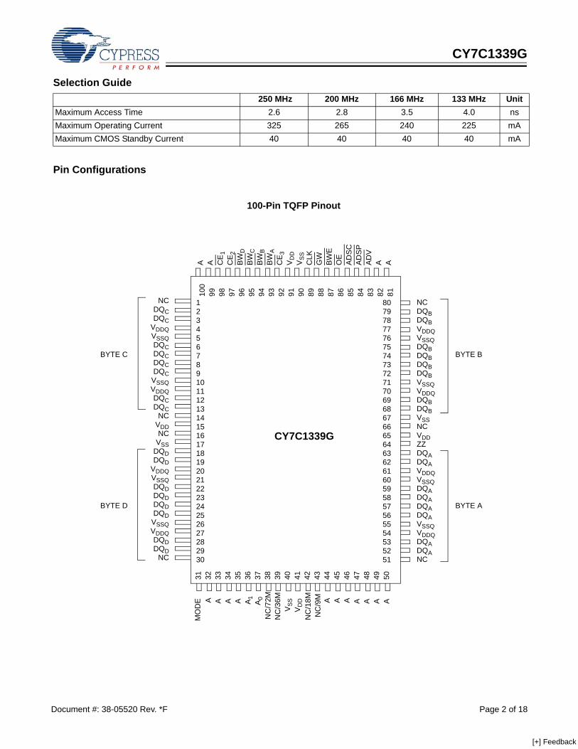
Selection Guide 250 MHz 200 MHz 166 MHz 133 MHz Unit
Maximum Access Time 2.6 2.8 3.5 4.0 nsMaximum Operating Current 325 265 240 225 mAMaximum CMOS Standby Current 40 40 40 40 mA
A A A A A 1 A0
NC
/72M
NC
/36M
VS
SV
DD
NC
/18M
NC
/9M A A A A A A A
NCDQBDQBVDDQVSSQDQBDQBDQBDQBVSSQVDDQDQBDQBVSSNCVDDZZDQADQAVDDQVSSQDQADQADQADQAVSSQVDDQDQADQANC
NCDQCDQC
VDDQVSSQDQCDQCDQCDQC
VSSQVDDQDQCDQC
NCVDDNC
VSSDQDDQD
VDDQVSSQDQDDQDDQDDQD
VSSQVDDQDQDDQD
NC
A A CE
1C
E2
BW
DB
WC
BW
BB
WA
CE
3V
DD
VS
SC
LKG
WB
WE
OE
AD
SC
AD
SP
AD
VA A
123456789101112131415161718192021222324252627282930
31 32 33 34 35 36 37 38 39 40 41 42 43 44 45 46 47 48 49 50
807978777675747372717069686766656463626160595857565554535251
100
99 98 97 96 95 94 93 92 91 90 89 88 87 86 85 84 83 82 81
MO
DE
BYTE A
BYTE B
BYTE D
BYTE C
CY7C1339G
100-Pin TQFP Pinout
[+] Feedback

CY7C1339G
Document #: 38-05520 Rev. *F Page 3 of 18
Pin Configurations (continued)
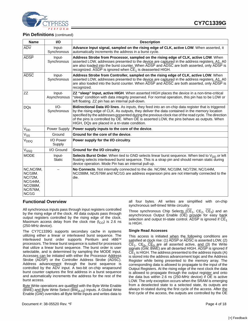
Pin DefinitionsName I/O Description
A0, A1, A Input-Synchronous
Address Inputs used to select one of the 128K address locations. Sampled at the rising edge of the CLK if ADSP or ADSC is active LOW, and CE1, CE2, and CE3 are sampled active. A1, A0 are fed to the two-bit counter..
BWA, BWBBWC, BWD
Input-Synchronous
Byte Write Select Inputs, active LOW. Qualified with BWE to conduct byte writes to the SRAM. Sampled on the rising edge of CLK.
GW Input-Synchronous
Global Write Enable Input, active LOW. When asserted LOW on the rising edge of CLK, a global write is conducted (ALL bytes are written, regardless of the values on BW[A:D] and BWE).
BWE Input-Synchronous
Byte Write Enable Input, active LOW. Sampled on the rising edge of CLK. This signal must be asserted LOW to conduct a byte write.
CLK Input-Clock
Clock Input. Used to capture all synchronous inputs to the device. Also used to increment the burst counter when ADV is asserted LOW, during a burst operation.
CE1 Input-Synchronous
Chip Enable 1 Input, active LOW. Sampled on the rising edge of CLK. Used in conjunction with CE2 and CE3 to select/deselect the device. ADSP is ignored if CE1 is HIGH. CE1 is sampled only when a new external address is loaded.
CE2 Input-Synchronous
Chip Enable 2 Input, active HIGH. Sampled on the rising edge of CLK. Used in conjunction with CE1 and CE3 to select/deselect the device.CE2 is sampled only when a new external address is loaded.
CE3 Input-Synchronous
Chip Enable 3 Input, active LOW. Sampled on the rising edge of CLK. Used in conjunction with CE1 and CE2 to select/deselect the device. CE3 is sampled only when a new external address is loaded. Not connected for BGA. Where referenced, CE3 is assumed active throughout this document for BGA.
OE Input-Asynchronous
Output Enable, asynchronous input, active LOW. Controls the direction of the I/O pins. When LOW, the I/O pins behave as outputs. When deasserted HIGH, I/O pins are tri-stated, and act as input data pins. OE is masked during the first clock of a read cycle when emerging from a deselected state.
2 3 4 5 6 71ABCDEFGHJKLMN
PRTU
VDDQ
NC/288MNC/144M
NCDQC
DQD
DQC
DQD
A A A AADSP VDDQ
CE2 A
DQCVDDQDQC
VDDQ
VDDQ
VDDQ
DQD
DQD
NCNC
VDDQ
VDD
CLK
VDD
VSS
VSS
VSS
VSS
VSS
VSS
VSS
VSS
NC/576MNC/1G
NC
NC
NCNCNCNCNC/36MNC/72M
NC
VDDQ
VDDQ
VDDQ
A A AA
NC/9MAA
AAA
AA0
A1
DQA
DQC
DQA
DQA
DQA
DQBDQB
DQBDQB
DQBDQBDQB
DQA
DQA
DQA
DQA
DQBVDD
DQCDQCDQCVDDDQD
DQDDQDDQD
ADSC
NCCE1OE
ADVGW
VSSVSSVSS
VSS
VSS
VSSVSS
VSS NCMODE
NC
NC
BWBBWc
NC VDD NC
BWANCBWE
BWD
ZZ
119-Ball BGA Pinout
[+] Feedback
CY7C1339G
Document #: 38-05520 Rev. *F Page 4 of 18
Functional OverviewAll synchronous inputs pass through input registers controlledby the rising edge of the clock. All data outputs pass throughoutput registers controlled by the rising edge of the clock.Maximum access delay from the clock rise (tCO) is 2.6 ns(250-MHz device). The CY7C1339G supports secondary cache in systemsutilizing either a linear or interleaved burst sequence. Theinterleaved burst order supports Pentium and i486™processors. The linear burst sequence is suited for processorsthat utilize a linear burst sequence. The burst order is userselectable, and is determined by sampling the MODE input.Accesses can be initiated with either the Processor AddressStrobe (ADSP) or the Controller Address Strobe (ADSC).Address advancement through the burst sequence iscontrolled by the ADV input. A two-bit on-chip wraparoundburst counter captures the first address in a burst sequenceand automatically increments the address for the rest of theburst access.Byte Write operations are qualified with the Byte Write Enable(BWE) and Byte Write Select (BW[A:D]) inputs. A Global WriteEnable (GW) overrides all Byte Write inputs and writes data to
all four bytes. All writes are simplified with on-chipsynchronous self-timed Write circuitry.Three synchronous Chip Selects (CE1, CE2, CE3) and anasynchronous Output Enable (OE) provide for easy bankselection and output tri-state control. ADSP is ignored if CE1is HIGH.
Single Read AccessesThis access is initiated when the following conditions aresatisfied at clock rise: (1) ADSP or ADSC is asserted LOW, (2)CE1, CE2, CE3 are all asserted active, and (3) the Writesignals (GW, BWE) are all deserted HIGH. ADSP is ignored ifCE1 is HIGH. The address presented to the address inputs (A)is stored into the address advancement logic and the AddressRegister while being presented to the memory array. Thecorresponding data is allowed to propagate to the input of theOutput Registers. At the rising edge of the next clock the datais allowed to propagate through the output register and ontothe data bus within 2.6 ns (250-MHz device) if OE is activeLOW. The only exception occurs when the SRAM is emergingfrom a deselected state to a selected state, its outputs arealways tri-stated during the first cycle of the access. After thefirst cycle of the access, the outputs are controlled by the OE
ADV Input-Synchronous
Advance Input signal, sampled on the rising edge of CLK, active LOW. When asserted, it automatically increments the address in a burst cycle.
ADSP Input-Synchronous
Address Strobe from Processor, sampled on the rising edge of CLK, active LOW. When asserted LOW, addresses presented to the device are captured in the address registers. A1, A0 are also loaded into the burst counter. When ADSP and ADSC are both asserted, only ADSP is recognized. ASDP is ignored when CE1 is deasserted HIGH.
ADSC Input-Synchronous
Address Strobe from Controller, sampled on the rising edge of CLK, active LOW. When asserted LOW, addresses presented to the device are captured in the address registers. A1, A0 are also loaded into the burst counter. When ADSP and ADSC are both asserted, only ADSP is recognized.
ZZ Input-Asynchronous
ZZ “sleep” Input, active HIGH. When asserted HIGH places the device in a non-time-critical “sleep” condition with data integrity preserved. For normal operation, this pin has to be LOW or left floating. ZZ pin has an internal pull-down.
DQs I/O-Synchronous
Bidirectional Data I/O lines. As inputs, they feed into an on-chip data register that is triggered by the rising edge of CLK. As outputs, they deliver the data contained in the memory location specified by the addresses presented during the previous clock rise of the read cycle. The direction of the pins is controlled by OE. When OE is asserted LOW, the pins behave as outputs. When HIGH, DQs are placed in a tri-state condition.
VDD Power Supply Power supply inputs to the core of the device. VSS Ground Ground for the core of the device. VDDQ I/O Power
SupplyPower supply for the I/O circuitry.
VSSQ I/O Ground Ground for the I/O circuitry. MODE Input-
StaticSelects Burst Order. When tied to GND selects linear burst sequence. When tied to VDD or left floating selects interleaved burst sequence. This is a strap pin and should remain static during device operation. Mode Pin has an internal pull-up.
NC,NC/9M,NC/18M.NC/72M, NC/144M, NC/288M,NC/576M,NC/1G
– No Connects. Not internally connected to the die. NC/9M, NC/18M, NC/72M, NC/144M, NC/288M, NC/576M and NC/1G are address expansion pins are not internally connected to the die.
Pin Definitions (continued)
Name I/O Description
[+] Feedback

CY7C1339G
Document #: 38-05520 Rev. *F Page 5 of 18
signal. Consecutive single Read cycles are supported. Oncethe SRAM is deselected at clock rise by the chip select andeither ADSP or ADSC signals, its output will tri-state immedi-ately.
Single Write Accesses Initiated by ADSPThis access is initiated when both of the following conditionsare satisfied at clock rise: (1) ADSP is asserted LOW, and(2) CE1, CE2, CE3 are all asserted active. The addresspresented to A is loaded into the address register and theaddress advancement logic while being delivered to thememory array. The Write signals (GW, BWE, and BW[A:D]) andADV inputs are ignored during this first cycle. ADSP-triggered Write accesses require two clock cycles tocomplete. If GW is asserted LOW on the second clock rise, thedata presented to the DQs inputs is written into the corre-sponding address location in the memory array. If GW is HIGH,then the Write operation is controlled by BWE and BW[A:D]signals. The CY7C1339G provides Byte Write capability thatis described in the Write Cycle Descriptions table. Assertingthe Byte Write Enable input (BWE) with the selected ByteWrite (BW[A:D]) input, will selectively write to only the desiredbytes. Bytes not selected during a Byte Write operation willremain unaltered. A synchronous self-timed Write mechanismhas been provided to simplify the Write operations. Because the CY7C1339G is a common I/O device, the OutputEnable (OE) must be deserted HIGH before presenting datato the DQs inputs. Doing so will tri-state the output drivers. Asa safety precaution, DQs are automatically tri-stated whenevera Write cycle is detected, regardless of the state of OE.
Single Write Accesses Initiated by ADSCADSC Write accesses are initiated when the following condi-tions are satisfied: (1) ADSC is asserted LOW, (2) ADSP isdeserted HIGH, (3) CE1, CE2, CE3 are all asserted active, and(4) the appropriate combination of the Write inputs (GW, BWE,and BW[A:D]) are asserted active to conduct a Write to thedesired byte(s). ADSC-triggered Write accesses require asingle clock cycle to complete. The address presented to A isloaded into the address register and the addressadvancement logic while being delivered to the memory array.The ADV input is ignored during this cycle. If a global Write isconducted, the data presented to the DQs is written into thecorresponding address location in the memory core. If a ByteWrite is conducted, only the selected bytes are written. Bytesnot selected during a Byte Write operation will remainunaltered. A synchronous self-timed Write mechanism hasbeen provided to simplify the Write operations. Because the CY7C1339G is a common I/O device, the OutputEnable (OE) must be deserted HIGH before presenting data
to the DQs inputs. Doing so will tri-state the output drivers. Asa safety precaution, DQs are automatically tri-stated whenevera Write cycle is detected, regardless of the state of OE.
Burst SequencesThe CY7C1339G provides a two-bit wraparound counter, fedby A1, A0, that implements either an interleaved or linear burstsequence. The interleaved burst sequence is designed specif-ically to support Intel Pentium applications. The linear burstsequence is designed to support processors that follow alinear burst sequence. The burst sequence is user selectablethrough the MODE input.Asserting ADV LOW at clock rise will automatically incrementthe burst counter to the next address in the burst sequence.Both Read and Write burst operations are supported.
Sleep ModeThe ZZ input pin is an asynchronous input. Asserting ZZplaces the SRAM in a power conservation “sleep” mode. Twoclock cycles are required to enter into or exit from this “sleep”mode. While in this mode, data integrity is guaranteed.Accesses pending when entering the “sleep” mode are notconsidered valid nor is the completion of the operationguaranteed. The device must be deselected prior to enteringthe “sleep” mode. CE1, CE2, CE3, ADSP, and ADSC mustremain inactive for the duration of tZZREC after the ZZ inputreturns LOW.
Interleaved Burst Address Table (MODE = Floating or VDD)
FirstAddressA1, A0
SecondAddressA1, A0
ThirdAddressA1, A0
FourthAddressA1, A0
00 01 10 1101 00 11 1010 11 00 0111 10 01 00
Linear Burst Address Table (MODE = GND)First
AddressA1, A0
SecondAddressA1, A0
Third AddressA1, A0
FourthAddressA1, A0
00 01 10 1101 10 11 0010 11 00 0111 00 01 10
ZZ Mode Electrical CharacteristicsParameter Description Test Conditions Min. Max. Unit
IDDZZ Snooze mode standby current ZZ > VDD – 0.2V 40 mAtZZS Device operation to ZZ ZZ > VDD – 0.2V 2tCYC nstZZREC ZZ recovery time ZZ < 0.2V 2tCYC nstZZI ZZ active to snooze current This parameter is sampled 2tCYC nstRZZI ZZ Inactive to exit snooze current This parameter is sampled 0 ns
[+] Feedback
CY7C1339G
Document #: 38-05520 Rev. *F Page 6 of 18
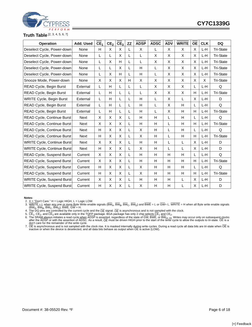
Truth Table [2, 3, 4, 5, 6, 7]
Operation Add. Used CE1 CE2 CE3 ZZ ADSP ADSC ADV WRITE OE CLK DQDeselect Cycle, Power-down None H X X L X L X X X L-H Tri-State
Deselect Cycle, Power-down None L L X L L X X X X L-H Tri-State
Deselect Cycle, Power-down None L X H L L X X X X L-H Tri-State
Deselect Cycle, Power-down None L L X L H L X X X L-H Tri-State
Deselect Cycle, Power-down None L X H L H L X X X L-H Tri-State
Snooze Mode, Power-down None X X X H X X X X X X Tri-State
READ Cycle, Begin Burst External L H L L L X X X L L-H Q
READ Cycle, Begin Burst External L H L L L X X X H L-H Tri-State
WRITE Cycle, Begin Burst External L H L L H L X L X L-H D
READ Cycle, Begin Burst External L H L L H L X H L L-H Q
READ Cycle, Begin Burst External L H L L H L X H H L-H Tri-State
READ Cycle, Continue Burst Next X X X L H H L H L L-H Q
READ Cycle, Continue Burst Next X X X L H H L H H L-H Tri-State
READ Cycle, Continue Burst Next H X X L X H L H L L-H Q
READ Cycle, Continue Burst Next H X X L X H L H H L-H Tri-State
WRITE Cycle, Continue Burst Next X X X L H H L L X L-H D
WRITE Cycle, Continue Burst Next H X X L X H L L X L-H D
READ Cycle, Suspend Burst Current X X X L H H H H L L-H Q
READ Cycle, Suspend Burst Current X X X L H H H H H L-H Tri-State
READ Cycle, Suspend Burst Current H X X L X H H H L L-H Q
READ Cycle, Suspend Burst Current H X X L X H H H H L-H Tri-State
WRITE Cycle, Suspend Burst Current X X X L H H H L X L-H D
WRITE Cycle, Suspend Burst Current H X X L X H H L X L-H D
Notes: 2. X = “Don't Care.” H = Logic HIGH, L = Logic LOW.3. WRITE = L when any one or more Byte Write enable signals (BWA, BWB, BWC, BWD) and BWE = L or GW= L. WRITE = H when all Byte write enable signals
(BWA, BWB, BWC, BWD), BWE, GW = H.4. The DQ pins are controlled by the current cycle and the OE signal. OE is asynchronous and is not sampled with the clock.5. CE1, CE2, and CE3 are available only in the TQFP package. BGA package has only 2 chip selects CE1 and CE2.6. The SRAM always initiates a read cycle when ADSP is asserted, regardless of the state of GW, BWE, or BW[A: D]. Writes may occur only on subsequent clocks
after the ADSP or with the assertion of ADSC. As a result, OE must be driven HIGH prior to the start of the write cycle to allow the outputs to tri-state. OE is a don't care for the remainder of the write cycle.
7. OE is asynchronous and is not sampled with the clock rise. It is masked internally during write cycles. During a read cycle all data bits are tri-state when OE is inactive or when the device is deselected, and all data bits behave as output when OE is active (LOW).
[+] Feedback

CY7C1339G
Document #: 38-05520 Rev. *F Page 7 of 18
Partial Truth Table for Read/Write [2, 8]
Function GW BWE BWD BWC BWB BWARead H H X X X X
Read H L H H H H
Write Byte A – DQA H L H H H L
Write Byte B – DQB H L H H L H
Write Bytes B, A H L H H L L
Write Byte C– DQC H L H L H H
Write Bytes C, A H L H L H L
Write Bytes C, B H L H L L H
Write Bytes C, B, A H L H L L L
Write Byte D– DQD H L L H H H
Write Bytes D, A H L L H H L
Write Bytes D, B H L L H L H
Write Bytes D, B, A H L L H L L
Write Bytes D, C H L L L H H
Write Bytes D, C, A H L L L H L
Write Bytes D, C, B H L L L L H
Write All Bytes H L L L L L
Write All Bytes L X X X X X
Note: 8.Table only lists a partial listing of the byte write combinations. Any combination of BWX is valid. Appropriate write will be done based on which byte write is active.
[+] Feedback

CY7C1339G
Document #: 38-05520 Rev. *F Page 8 of 18
Maximum Ratings(Above which the useful life may be impaired. For user guide-lines, not tested.)Storage Temperature .................................–65°C to +150°CAmbient Temperature withPower Applied.............................................–55°C to +125°CSupply Voltage on VDD Relative to GND........ –0.5V to +4.6VSupply Voltage on VDDQ Relative to GND ...... –0.5V to +VDDDC Voltage Applied to Outputsin tri-state ............................................ –0.5V to VDDQ + 0.5V
DC Input Voltage ................................... –0.5V to VDD + 0.5VCurrent into Outputs (LOW)......................................... 20 mAStatic Discharge Voltage.......................................... > 2001V(per MIL-STD-883, Method 3015)Latch-up Current.................................................... > 200 mAOperating Range
RangeAmbient
Temperature VDD VDDQCommercial 0°C to +70°C 3.3V
–5%/+10%2.5V –5%
to VDDIndustrial –40°C to +85°C Automotive –40°C to +125°C
Electrical Characteristics Over the Operating Range[9, 10]
Parameter Description Test Conditions Min. Max. UnitVDD Power Supply Voltage 3.135 3.6 V
VDDQ I/O Supply Voltage 2.375 VDD V
VOH Output HIGH Voltage for 3.3V I/O, IOH = –4.0 mA 2.4 V
for 2.5V I/O, IOH = –1.0 mA 2.0 V
VOL Output LOW Voltage for 3.3V I/O, IOL = 8.0 mA 0.4 V
for 2.5V I/O, IOL = 1.0 mA 0.4 V
VIH Input HIGH Voltage[9] for 3.3V I/O 2.0 VDD + 0.3V V
for 2.5V I/O 1.7 VDD + 0.3V V
VIL Input LOW Voltage[9] for 3.3V I/O –0.3 0.8 V
for 2.5V I/O –0.3 0.7 V
IX Input Leakage Current except ZZ and MODE
GND ≤ VI ≤ VDDQ –5 5 µA
Input Current of MODE Input = VSS –30 µA
Input = VDD 5 µA
Input Current of ZZ Input = VSS –5 µA
Input = VDD 30 µA
IOZ Output Leakage Current GND ≤ VI ≤ VDDQ, Output Disabled –5 5 µA
IDD VDD Operating Supply Current
VDD = Max., IOUT = 0 mA,f = fMAX = 1/tCYC
4-ns cycle, 250 MHz 325 mA
5-ns cycle, 200 MHz 265 mA
6-ns cycle, 166 MHz 240 mA
7.5-ns cycle, 133 MHz 225 mA
ISB1 Automatic CE Power-down Current—TTL Inputs
VDD = Max, Device Deselected, VIN ≥ VIH or VIN ≤ VILf = fMAX = 1/tCYC
4-ns cycle, 250 MHz 120 mA
5-ns cycle, 200 MHz 110 mA
6-ns cycle, 166 MHz 100 mA
Industrial/Commercial
7.5-ns cycle, 133 MHz 90 mA
Automotive 7.5-ns cycle, 133 MHz 115 mA
ISB2 Automatic CEPower-down Current—CMOS Inputs
VDD = Max, Device Deselected, VIN ≤ 0.3V or VIN > VDDQ – 0.3V, f = 0
All speeds 40 mA
Notes: 9. Overshoot: VIH(AC) < VDD +1.5V (Pulse width less than tCYC/2), undershoot: VIL(AC) > –2V (Pulse width less than tCYC/2).10. TPower-up: Assumes a linear ramp from 0V to VDD(min.) within 200 ms. During this time VIH < VDD and VDDQ < VDD.
[+] Feedback

CY7C1339G
Document #: 38-05520 Rev. *F Page 9 of 18
ISB3 Automatic CE Power-down Current—CMOS Inputs
VDD = Max, Device Deselected, or VIN ≤ 0.3V or VIN > VDDQ – 0.3Vf = fMAX = 1/tCYC
4-ns cycle, 250 MHz 105 mA
5-ns cycle, 200 MHz 95 mA
6-ns cycle, 166 MHz 85 mA
7.5-ns cycle, 133 MHz 75 mA
ISB4 Automatic CE Power-down Current—TTL Inputs
VDD = Max, Device Deselected, VIN ≥ VIH or VIN ≤ VIL, f = 0
All Speeds 45 mA
Capacitance[11]
Parameter Description Test ConditionsTQFP
PackageBGA
Package UnitCIN Input Capacitance TA = 25°C, f = 1 MHz,
VDD = 3.3V.VDDQ = 3.3V
5 5 pFCCLK Clock Input Capacitance 5 5 pFCI/O Input/Output Capacitance 5 7 pF
Thermal Resistance[11]
Parameter Description Test ConditionsTQFP
PackageBGA
Package UnitΘJA Thermal Resistance
(Junction to Ambient)Test conditions follow standard test methods and procedures for measuring thermal impedance, per EIA/JESD51
30.32 34.1 °C/W
ΘJC Thermal Resistance(Junction to Case)
6.85 14.0 °C/W
AC Test Loads and Waveforms
Note: 11. Tested initially and after any design or process change that may affect these parameters.
Electrical Characteristics Over the Operating Range[9, 10] (continued)
Parameter Description Test Conditions Min. Max. Unit
OUTPUT
R = 317Ω
R = 351Ω5 pF
INCLUDINGJIG ANDSCOPE
(a) (b)
OUTPUT
RL = 50ΩZ0 = 50Ω
VT = 1.5V
3.3V ALL INPUT PULSESVDDQ
GND
90%10%
90%10%
≤ 1 ns ≤ 1 ns
(c)
OUTPUT
R = 1667Ω
R = 1538Ω5 pF
INCLUDINGJIG ANDSCOPE
(a) (b)
OUTPUT
RL = 50ΩZ0 = 50Ω
VT = 1.25V
2.5V ALL INPUT PULSESVDDQ
GND
90%10%
90%10%
≤ 1 ns ≤ 1 ns
(c)
3.3V I/O Test Load
2.5V I/O Test Load
OUTPUT
R = 1667Ω
R = 1538Ω5 pF
INCLUDINGJIG ANDSCOPE
(a) (b)
OUTPUT
RL = 50ΩZ0 = 50Ω
VT = 1.25V
2.5V ALL INPUT PULSESVDDQ
GND
90%10%
90%10%
≤ 1 ns ≤ 1 ns
(c)
2.5V I/O Test Load
[+] Feedback

CY7C1339G
Document #: 38-05520 Rev. *F Page 10 of 18
Switching Characteristics Over the Operating Range[12, 13, 14, 15, 16, 17]
Parameter Description–250 –200 –166 –133
UnitMin. Max. Min. Max. Min. Max. Min. Max.tPOWER VDD(Typical) to the first Access[12] 1 1 1 1 ms
ClocktCYC Clock Cycle Time 4.0 5.0 6.0 7.5 ns
tCH Clock HIGH 1.7 2.0 2.5 3.0 ns
tCL Clock LOW 1.7 2.0 2.5 3.0 ns
Output TimestCO Data Output Valid After CLK Rise 2.6 2.8 3.5 4.0 ns
tDOH Data Output Hold After CLK Rise 1.0 1.0 1.5 1.5 ns
tCLZ Clock to Low-Z[13, 14, 15] 0 0 0 0 ns
tCHZ Clock to High-Z[13, 14, 15] 2.6 2.8 3.5 4.0 ns
tOEV OE LOW to Output Valid 2.6 2.8 3.5 4.0 ns
tOELZ OE LOW to Output Low-Z[13, 14, 15] 0 0 0 0 ns
tOEHZ OE HIGH to Output High-Z[13, 14, 15] 2.6 2.8 3.5 4.0 ns
Set-up TimestAS Address Set-up Before CLK Rise 1.2 1.2 1.5 1.5 ns
tADS ADSC, ADSP Set-up Before CLK Rise 1.2 1.2 1.5 1.5 ns
tADVS ADV Set-up Before CLK Rise 1.2 1.2 1.5 1.5 ns
tWES GW, BWE, BWX Set-up Before CLK Rise 1.2 1.2 1.5 1.5 ns
tDS Data Input Set-up Before CLK Rise 1.2 1.2 1.5 1.5 ns
tCES Chip Enable Set-Up Before CLK Rise 1.2 1.2 1.5 1.5 ns
Hold TimestAH Address Hold After CLK Rise 0.3 0.5 0.5 0.5 ns
tADH ADSP, ADSC Hold After CLK Rise 0.3 0.5 0.5 0.5 ns
tADVH ADV Hold After CLK Rise 0.3 0.5 0.5 0.5 ns
tWEH GW, BWE, BWX Hold After CLK Rise 0.3 0.5 0.5 0.5 ns
tDH Data Input Hold After CLK Rise 0.3 0.5 0.5 0.5 ns
tCEH Chip Enable Hold After CLK Rise 0.3 0.5 0.5 0.5 ns
Notes: 12. This part has a voltage regulator internally; tPOWER is the time that the power needs to be supplied above VDD(minimum) initially before a read or write operation
can be initiated.13. tCHZ, tCLZ,tOELZ, and tOEHZ are specified with AC test conditions shown in part (b) of AC Test Loads. Transition is measured ± 200 mV from steady-state voltage.14. At any given voltage and temperature, tOEHZ is less than tOELZ and tCHZ is less than tCLZ to eliminate bus contention between SRAMs when sharing the same
data bus. These specifications do not imply a bus contention condition, but reflect parameters guaranteed over worst case user conditions. Device is designed to achieve High-Z prior to Low-Z under the same system conditions.
15. This parameter is sampled and not 100% tested.16. Timing reference level is 1.5V when VDDQ = 3.3V and is 1.25V when VDDQ = 2.5V.17. Test conditions shown in (a) of AC Test Loads unless otherwise noted.
[+] Feedback

CY7C1339G
Document #: 38-05520 Rev. *F Page 11 of 18
Switching WaveformsRead Cycle Timing[18]
Note: 18. On this diagram, when CE is LOW, CE1 is LOW, CE2 is HIGH and CE3 is LOW. When CE is HIGH, CE1 is HIGH or CE2 is LOW or CE3 is HIGH.
tCYC
tCL
CLK
ADSP
tADH
tADS
ADDRESS
tCH
OE
ADSC
CE
tAHtAS
A1
tCEHtCES
GW, BWE,
BW[A:D]
Data Out (Q) High-Z
tCLZtDOH
tCO
ADV
tOEHZ
tCO
Single READ BURST READ
tOEV
tOELZtCHZ
ADV suspends burst.
Burst wraps aroundto its initial state
tADVHtADVS
tWEHtWES
tADHtADS
Q(A2) Q(A2 + 1) Q(A2 + 2)Q(A1) Q(A2) Q(A2 + 1)Q(A2 + 3)
A2 A3
Deselectcycle
Burst continued withnew base address
DON’T CARE UNDEFINED
[+] Feedback

CY7C1339G
Document #: 38-05520 Rev. *F Page 12 of 18
Write Cycle Timing[18, 19]
Note: 19. Full width write can be initiated by either GW LOW; or by GW HIGH, BWE LOW and BW[A:D] LOW.
Switching Waveforms (continued)
tCYC
tCLCLK
ADSP
tADHtADS
ADDRESS
tCH
OE
ADSC
CE
tAHtAS
A1
tCEHtCES
BWE,
BW[A :D]
Data Out (Q)
High-Z
ADV
BURST READ BURST WRITE
D(A2) D(A2 + 1) D(A2 + 1)D(A1) D(A3) D(A3 + 1) D(A3 + 2)D(A2 + 3)
A2 A3
Data In (D)
Extended BURST WRITE
D(A2 + 2)
Single WRITE
tADHtADStADHtADS
tOEHZ
tADVH
tADVS
tWEHtWES
tDHtDS
GW
tWEHtWES
Byte write signals areignored for first cycle whenADSP initiates burst
ADSC extends burst
ADV suspends burst
DON’T CARE UNDEFINED
[+] Feedback

CY7C1339G
Document #: 38-05520 Rev. *F Page 13 of 18
Read/Write Cycle Timing[18, 20, 21]
Notes: 20. The data bus (Q) remains in high-Z following a WRITE cycle, unless a new read access is initiated by ADSP or ADSC.21. GW is HIGH.
Switching Waveforms (continued)
tCYC
tCL
CLK
ADSP
tADHtADS
ADDRESS
tCH
OE
ADSC
CE
tAHtAS
A2
tCEHtCES
BWE,
BW[A:D]
Data Out (Q) High-Z
ADV
Single WRITE
D(A3)
A4 A5 A6
D(A5) D(A6)Data In (D)
BURST READBack-to-Back READs
High-Z
Q(A2)Q(A1) Q(A4) Q(A4+1) Q(A4+2)
tWEHtWES
Q(A4+3)
tOEHZ
tDHtDS
tOELZ
tCLZ
tCO
Back-to-BackWRITEs
A1
DON’T CARE UNDEFINED
A3
[+] Feedback

CY7C1339G
Document #: 38-05520 Rev. *F Page 14 of 18
ZZ Mode Timing [22, 23]
Notes: 22. Device must be deselected when entering ZZ mode. See Cycle Descriptions table for all possible signal conditions to deselect the device.23. DQs are in high-Z when exiting ZZ sleep mode.
Switching Waveforms (continued)
tZZ
I SUPPLY
CLK
ZZ
tZZREC
ALL INPUTS
(except ZZ)
DON’T CARE
I DDZZ
tZZI
tRZZI
Outputs (Q) High-Z
DESELECT or READ Only
[+] Feedback

CY7C1339G
Document #: 38-05520 Rev. *F Page 15 of 18
Ordering InformationNot all of the speed, package and temperature ranges are available. Please contact your local sales representative or
visit www.cypress.com for actual products offered.Speed(MHz) Ordering Code
PackageDiagram Package Type
OperatingRange
133 CY7C1339G-133AXC 51-85050 100-pin Thin Quad Flat Pack (14 x 20 x 1.4 mm) Lead-Free CommercialCY7C1339G-133BGC 51-85115 119-ball Ball Grid Array (14 x 22 x 2.4 mm)CY7C1339G-133BGXC 119-ball Ball Grid Array (14 x 22 x 2.4 mm) Lead-FreeCY7C1339G-133AXI 51-85050 100-pin Thin Quad Flat Pack (14 x 20 x 1.4 mm) Lead-Free IndustrialCY7C1339G-133BGI 51-85115 119-ball Ball Grid Array (14 x 22 x 2.4 mm)CY7C1339G-133BGXI 119-ball Ball Grid Array (14 x 22 x 2.4 mm) Lead-FreeCY7C1339G-133AXE 51-85050 100-pin Thin Quad Flat Pack (14 x 20 x 1.4 mm) Lead-Free Automotive
166 CY7C1339G-166AXC 51-85050 100-pin Thin Quad Flat Pack (14 x 20 x 1.4 mm) Lead-Free CommercialCY7C1339G-166BGC 51-85115 119-ball Ball Grid Array (14 x 22 x 2.4 mm)CY7C1339G-166BGXC 119-ball Ball Grid Array (14 x 22 x 2.4 mm) Lead-FreeCY7C1339G-166AXI 51-85050 100-pin Thin Quad Flat Pack (14 x 20 x 1.4 mm) Lead-Free IndustrialCY7C1339G-166BGI 51-85115 119-ball Ball Grid Array (14 x 22 x 2.4 mm)CY7C1339G-166BGXI 119-ball Ball Grid Array (14 x 22 x 2.4 mm) Lead-Free
200 CY7C1339G-200AXC 51-85050 100-pin Thin Quad Flat Pack (14 x 20 x 1.4 mm) Lead-Free CommercialCY7C1339G-200BGC 51-85115 119-ball Ball Grid Array (14 x 22 x 2.4 mm)CY7C1339G-200BGXC 119-ball Ball Grid Array (14 x 22 x 2.4 mm) Lead-FreeCY7C1339G-200AXI 51-85050 100-pin Thin Quad Flat Pack (14 x 20 x 1.4 mm) Lead-Free IndustrialCY7C1339G-200BGI 51-85115 119-ball Ball Grid Array (14 x 22 x 2.4 mm)CY7C1339G-200BGXI 119-ball Ball Grid Array (14 x 22 x 2.4 mm) Lead-Free
250 CY7C1339G-250AXC 51-85050 100-pin Thin Quad Flat Pack (14 x 20 x 1.4 mm) Lead-Free CommercialCY7C1339G-250BGC 51-85115 119-ball Ball Grid Array (14 x 22 x 2.4 mm)CY7C1339G-250BGXC 119-ball Ball Grid Array (14 x 22 x 2.4 mm) Lead-FreeCY7C1339G-250AXI 51-85050 100-pin Thin Quad Flat Pack (14 x 20 x 1.4 mm) Lead-Free IndustrialCY7C1339G-250BGI 51-85115 119-ball Ball Grid Array (14 x 22 x 2.4 mm)CY7C1339G-250BGXI 119-ball Ball Grid Array (14 x 22 x 2.4 mm) Lead-Free
[+] Feedback

CY7C1339G
Document #: 38-05520 Rev. *F Page 16 of 18
Package Diagrams
NOTE:
1. JEDEC STD REF MS-026
2. BODY LENGTH DIMENSION DOES NOT INCLUDE MOLD PROTRUSION/END FLASH
MOLD PROTRUSION/END FLASH SHALL NOT EXCEED 0.0098 in (0.25 mm) PER SIDE
3. DIMENSIONS IN MILLIMETERS
BODY LENGTH DIMENSIONS ARE MAX PLASTIC BODY SIZE INCLUDING MOLD MISMATCH
0.30±0.08
0.65
20.0
0±0.
10
22.0
0±0.
20
1.40±0.05
12°±1°
1.60 MAX.
0.05 MIN.
0.60±0.15
0° MIN.
0.25
0°-7°
(8X)
STAND-OFF
R 0.08 MIN.
TYP.
0.20 MAX.
0.15 MAX.
0.20 MAX.
R 0.08 MIN.0.20 MAX.
14.00±0.10
16.00±0.20
0.10
SEE DETAIL A
DETAIL A
1
100
30
31 50
51
80
81
GAUGE PLANE
1.00 REF.
0.20 MIN.
SEATING PLANE
100-Pin TQFP (14 x 20 x 1.4 mm) (51-85050)
51-85050-*B
[+] Feedback

CY7C1339G
Document #: 38-05520 Rev. *F Page 17 of 18© Cypress Semiconductor Corporation, 2006. The information contained herein is subject to change without notice. Cypress Semiconductor Corporation assumes no responsibility for the useof any circuitry other than circuitry embodied in a Cypress product. Nor does it convey or imply any license under patent or other rights. Cypress products are not warranted nor intended to beused for medical, life support, life saving, critical control or safety applications, unless pursuant to an express written agreement with Cypress. Furthermore, Cypress does not authorize itsproducts for use as critical components in life-support systems where a malfunction or failure may reasonably be expected to result in significant injury to the user. The inclusion of Cypressproducts in life-support systems application implies that the manufacturer assumes all risk of such use and in doing so indemnifies Cypress against all charges.
Package Diagrams (continued)
1.27
20.3
2
21 6543 7
L
E
A
B
D
C
H
G
F
K
J
U
P
N
M
T
R
12.00
19.5
0
30° TYP.
2.40
MA
X.
A1 CORNER
0.70 REF.
U
T
R
P
N
M
L
K
J
H
G
F
E
D
C
A
B
2 14 36 57Ø1.00(3X) REF.
7.62
22.0
0±0.
20
14.00±0.20
1.27
0.60
±0.
10
C
0.15
C
B
A
0.15(4X)
Ø0.05 M C
Ø0.75±0.15(119X)
Ø0.25 M C A B
SEATING PLANE
0.90
±0.
05
3.81
10.1
6
0.25
C
0.56
51-85115-*B
119-Ball BGA (14 x 22 x 2.4 mm) (51-85115)
All products and company names mentioned in this document may be the trademarks of their respective holders.
[+] Feedback
CY7C1339G
Document #: 38-05520 Rev. *F Page 18 of 18
Document History Page
Document Title: CY7C1339G 4-Mbit (128K x 32) Pipelined Sync SRAMDocument Number: 38-05520
REV. ECN NO. Issue DateOrig. of Change Description of Change
** 224368 See ECN RKF New data sheet*A 288909 See ECN VBL In Ordering Info section, Changed TQFP to PB-free TQFP
Added PB-free BG package*B 332895 See ECN SYT Modified Address Expansion balls in the pinouts for 100 TQFP and 119 BGA
Package as per JEDEC standards and updated the Pin Definitions accordinglyModified VOL, VOH test conditionsReplaced TBDs for ΘJA and ΘJC to their respective values on the Thermal Resis-tance table Updated the Ordering Information by shading and unshading MPNs as per availability
*C 351194 See ECN PCI Updated Ordering Information Table*D 366728 See ECN PCI Added VDD/VDDQ test conditions in DC Table
Modified test condition in note# 10 from VIH < VDD to VIH < VDD*E 420883 See ECN RXU Converted from Preliminary to Final
Changed address of Cypress Semiconductor Corporation on Page# 1 from “3901 North First Street” to “198 Champion Court”Modified “Input Load” to “Input Leakage Current except ZZ and MODE” in the Electrical Characteristics TableReplaced Package Name column with Package Diagram in the Ordering Infor-mation tableReplaced Package Diagram of 51-85050 from *A to *BAdded Automotive Range in Operating Range TableUpdated the Ordering Information
*F 480368 See ECN VKN Added the Maximum Rating for Supply Voltage on VDDQ Relative to GND.Updated the Ordering Information table.
[+] Feedback