Embed Size (px)
Citation preview
Copyright 2019 FUJITSU SEMICONDUCTOR LIMITED 2019.02
DS501-00024-5v0-E FUJITSU SEMICONDUCTOR DATA SHEET
Memory FRAM
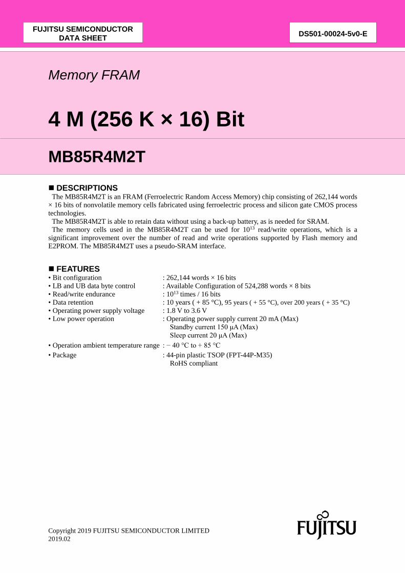
4 M (256 K × 16) Bit MB85R4M2T DESCRIPTIONS The MB85R4M2T is an FRAM (Ferroelectric Random Access Memory) chip consisting of 262,144 words
× 16 bits of nonvolatile memory cells fabricated using ferroelectric process and silicon gate CMOS process technologies. The MB85R4M2T is able to retain data without using a back-up battery, as is needed for SRAM. The memory cells used in the MB85R4M2T can be used for 1013 read/write operations, which is a
significant improvement over the number of read and write operations supported by Flash memory and E2PROM. The MB85R4M2T uses a pseudo-SRAM interface.
FEATURES • Bit configuration : 262,144 words × 16 bits • LB and UB data byte control : Available Configuration of 524,288 words × 8 bits • Read/write endurance : 1013 times / 16 bits • Data retention : 10 years ( + 85 °C), 95 years ( + 55 °C), over 200 years ( + 35 °C) • Operating power supply voltage : 1.8 V to 3.6 V • Low power operation : Operating power supply current 20 mA (Max) Standby current 150 μA (Max) Sleep current 20 μA (Max) • Operation ambient temperature range : − 40 °C to + 85 °C
• Package : 44-pin plastic TSOP (FPT-44P-M35) RoHS compliant

2 DS501-00024-5v0-E
MB85R4M2T
PIN ASSIGNMENTS
12345678910111213141516171819202122
44434241403938373635343332313029282726252423
A5A6A7/OE/UB/LBI/O15I/O14I/O13I/O12VSSVDDI/O11I/O10I/O9I/O8/ZZA8A9A10A11A12
FPT-44P-M35
(TOP VIEW)
A4A3A2A1A0
/CEI/O0I/O1I/O2I/O3VDDVSSI/O4I/O5I/O6I/O7/WEA17A16A15A14A13

DS501-00024-5v0-E 3
MB85R4M2T
PIN DESCRIPTIONS Pin Number Pin Name Functional Description
1 to 5, 18 to 22, 23 to 27, 42 to 44
A0 to A17 Address Input pins Select 262,144 words in FRAM memory array by 18 Address Input pins. When these address inputs are changed during /CE equals to “L” level, reading operation of data selected in the address after transition will start.
7 to 10, 13 to 16, 29 to 32, 35 to 38
I/O0 to I/O15 Data Input/Output pins These are 16 bits bidirectional pins for reading and writing.
6 /CE Chip Enable Input pin In case the /CE equals to “L” level and /ZZ equals to “H” level, device is activated and enables to start memory access. In writing operation, input data from I/O pins are latched at the rising edge of /CE and written to FRAM memory array.
17 /WE Write Enable Input pin Writing operation starts at the falling edge of /WE. Input data from I/O pins are latched at the rising edge of /WE and written to FRAM memory array.
41 /OE Output Enable Input pin When the /OE is “L” level, valid data are output to data bus. When the /OE is “H” level, all I/O pins become high impedance (High-Z) state.
28 /ZZ Sleep Mode Input pin When the /ZZ becomes to “L” level, device transits to the Sleep Mode. During reading and writing operation, /ZZ pin shall be hold “H” level.
39, 40 /LB, /UB Lower/Upper byte Control Input pins In case /LB or /UB equals to “L” level, it enables reading/writing operation of I/O0 to I/O7 or I/O8 to I/O15 respectively. In case /LB and /UB equal to “H” level, all I/O pins become High-Z state.
11, 33 VDD Supply Voltage pins Connect all two pins to the power supply.
12, 34 VSS Ground pins Connect all two pins to ground.
Note: Please refer to the timing diagram for functional description of each pin.

4 DS501-00024-5v0-E
MB85R4M2T
BLOCK DIAGRAM
FUNCTIONAL TRUTH TABLE Operation Mode /CE /WE /OE A0 to A17 /ZZ
Sleep × × × × L Standby H × × × H Read ↓ H L H or L H Address Access Read L H L ↑ or ↓ H Write(/CE Control)*1 ↓ L × H or L H Write(/WE Control)*1*2 L ↓ × H or L H Address Access Write*1*3 L ↓ × ↑ or ↓ H Pre-charge ↑ × × × H
Note: H= “H” level, L= “L” level, ↑= Rising edge, ↓= Falling edge, ×= H, L, ↓ or ↑ *1: In writing cycle, input data is latched at early rising edge of /CE or /WE. *2: In writing sequence of /WE control, there exists time with data output of reading cycle at the falling
edge of /CE. *3: In writing sequence of Address Access Write, there exists time with data output of reading cycle at the
address transition.
FRAM Array262,144×16
Column Decoder / Sense Amp./ Write Amp.
A0 to A17
/CE
/WE
/OE
/LB/UB
/ZZ
Address
Con
trolc
ircui
ts Row
Dec
oder
I/O0 to I/O15

DS501-00024-5v0-E 5
MB85R4M2T
State Transition Diagram
FUNCTIONAL TRUTH TABLE OF BYTE CONTROL Operation Mode /WE /OE /LB /UB I/O0 to I/O7 I/O8 to I/O15
Read(Without Output) H H × × Hi-Z Hi-Z H × H H Hi-Z Hi-Z
Read(I/O8 to I/O15) H L
H L Hi-Z Output Read(I/O0 to I/O7) L H Output Hi-Z Read(I/O0 to I/O15) L L Output Output Write(I/O8 to I/O15)
↑ × H L × Input
Write(I/O0 to I/O7) L H Input × Write(I/O0 to I/O15) L L Input Input
Note: H= “H” level, L= “L” level, ↑= Rising edge, ↓= Falling edge, ×= H, L, ↓ or ↑ Hi-Z= High Impedance
In case the byte reading or writing are not selected, /LB and /UB pins shall be connected to GND pin. In writing, please don’t switch /LB and/or /UB during /CE=”L”.
Standby RD/WROperation
Sleep
Power Up
/ZZ=L
/CE=L, /ZZ=H
/CE=H,/ZZ=H
/ZZ=H

6 DS501-00024-5v0-E
MB85R4M2T
ABABSOLUTE MAXIMUM RATINGS Parameter Symbol Rating Unit Min Max
Power Supply Voltage* VDD − 0.5 + 4.0 V Input Pin Voltage* VIN − 0.5 VDD + 0.5 ( ≤ 4.0) V Output Pin Voltage* VOUT − 0.5 VDD + 0.5 ( ≤ 4.0) V Operation Ambient Temperature TA − 40 + 85 °C Storage Temperature Tstg − 55 + 125 °C
* : All voltages are referenced to VSS (ground 0 V).
WARNING: Semiconductor devices can be permanently damaged by application of stress (voltage, current, temperature, etc.) in excess of absolute maximum ratings. Do not exceed these ratings.
RECOMMENDED OPERATING CONDITIONS Parameter Symbol Value Unit Min Typ Max
Power Supply Voltage*1 VDD 1.8 3.3 3.6 V Operation Ambient Temperature*2 TA − 40 ― + 85 °C
*1: All voltages are referenced to VSS (ground 0 V). *2: Ambient temperature when only this device is working. Please consider it to be the almost same as the
package surface temperature.
WARNING: The recommended operating conditions are required in order to ensure the normal operation of the semiconductor device. All of the device's electrical characteristics are warranted when the device is operated within these ranges. Always use semiconductor devices within their recommended operating condition ranges. Operation outside these ranges may adversely affect reliability and could result in device failure. No warranty is made with respect to uses, operating conditions, or combinations not represented on the data sheet. Users considering application outside the listed conditions are advised to contact their representatives beforehand.

DS501-00024-5v0-E 7
MB85R4M2T
ELECTRICAL CHARACTERISTICS 1. DC Characteristics
(within recommended operating conditions)
Parameter Symbol Condition Value Unit Min Typ Max Input Leakage Current |ILI| VIN = 0V to VDD ― ― 5 μA
Output Leakage Current |ILO| VOUT = 0V to VDD
/CE = VIH or /OE = VIH ― ― 5 μA
Operating Power Supply Current*1 IDD /CE = 0.2 V, Iout = 0 mA ― 15 20 mA
Standby Current ISB
/ZZ ≥ VDD − 0.2V /CE, /WE, /OE ≥ VDD − 0.2V /LB, /UB ≥ VDD − 0.2V Others ≥ VDD − 0.2V or ≤ 0.2V
― 30 150 μA
Sleep Current IZZ
/ZZ = VSS /CE, /WE, /OE ≥ VDD − 0.2V /LB, /UB ≥ VDD − 0.2V Others ≥ VDD − 0.2V or ≤ 0.2V
― 5 20 μA
High Level Input Voltage VIH VDD = 1.8V to 3.6V VDD × 0.8 ― VDD + 0.3 V
Low Level Input Voltage VIL VDD = 1.8V to 3.6V − 0.3 ― VDD × 0.17 V
High Level Output Voltage
VOH1 VDD = 2.7V to 3.6V IOH = − 1.0mA VDD × 0.8 ― ―
V VOH2
VDD = 1.8V to 2.7V IOH = − 100μA VDD − 0.2 ― ―
Low Level Output Voltage
VOL1 VDD = 2.7V to 3.6V IOL = 2.0mA ― ― 0.4
V VOL2
VDD = 1.8V to 2.7V IOL = 150μA ― ― 0.2
*1: During the measurement of IDD, all Address and I/O were taken to only change once per active cycle. Iout : output current
8 DS501-00024-5v0-E
MB85R4M2T
2. AC Characteristics ・AC Test Conditions
Power Supply Voltage : 1.8 V to 3.6 V Operation Ambient Temperature : − 40 °C to + 85 °C Input Voltage Amplitude : 0 V / VDD Input Rising Time : 3 ns Input Falling Time : 3 ns Input Evaluation Level : VDD/2 Output Evaluation Level : VDD/2 Output Load Capacitance : 30 pF
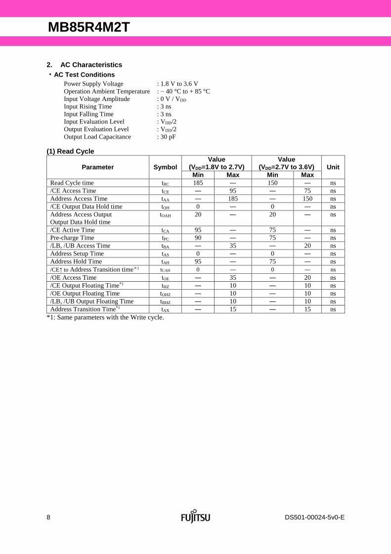
(1) Read Cycle
Parameter Symbol Value
(VDD=1.8V to 2.7V) Value
(VDD=2.7V to 3.6V) Unit Min Max Min Max
Read Cycle time tRC 185 ― 150 ― ns /CE Access Time tCE ― 95 ― 75 ns Address Access Time tAA ― 185 ― 150 ns /CE Output Data Hold time tOH 0 ― 0 ― ns Address Access Output Output Data Hold time
tOAH 20 ― 20 ― ns
/CE Active Time tCA 95 ― 75 ― ns Pre-charge Time tPC 90 ― 75 ― ns /LB, /UB Access Time tBA ― 35 ― 20 ns Address Setup Time tAS 0 ― 0 ― ns Address Hold Time tAH 95 ― 75 ― ns /CE↑ to Address Transition time*1 tCAH 0 ― 0 ― ns /OE Access Time tOE ― 35 ― 20 ns /CE Output Floating Time*1 tHZ ― 10 ― 10 ns /OE Output Floating Time tOHZ ― 10 ― 10 ns /LB, /UB Output Floating Time tBHZ ― 10 ― 10 ns Address Transition Time*1 tAX ― 15 ― 15 ns
*1: Same parameters with the Write cycle.

DS501-00024-5v0-E 9
MB85R4M2T
(2) Write Cycle
Parameter Symbol Value
(VDD=1.8V to 2.7V) Value
(VDD=2.7V to 3.6V) Unit Min Max Min Max
Write Cycle Time tWC 185 ― 150 ― ns /CE Active Time tCA 95 ― 75 ― ns /CE↓ to /WE↑ Time tCW 95 ― 75 ― ns Pre-charge Time tPC 90 ― 75 ― ns Write Pulse Width tWP 20 ― 20 ― ns Address Setup Time tAS 0 ― 0 ― ns Address Hold Time tAH 95 ― 75 ― ns /WE↓ to /CE↑ Time tWLC 20 ― 20 ― ns Address Transition to /WE↑ Time tAWH 185 ― 150 ― ns /WE↑ to Address Transition Time tWHA 0 ― 0 ― ns /LB, /UB Setup Time tBS 2 ― 2 ― ns /LB, /UB Hold Time tBH 0 ― 0 ― ns Data Setup Time tDS 10 ― 10 ― ns Data Hold Time tDH 0 ― 0 ― ns /WE Output Floating Time tWZ ― 10 ― 10 ns /WE Output Access Time*1 tWX 10 ― 10 ― ns Write Setup Time*1 tWS 0 ― 0 ― ns Write Hold Time*1 tWH 0 ― 0 ― ns
*1: Writing operation applies “Write Cycle Timing 1” or “Write Cycle Timing 2” by the relation of /CE and /WE timing. The values of tWX, tWS and tWH are defined by these operations. The conditions of tWS and tWH are not checked at shipping test.
(3) Power ON/OFF Sequence and Sleep Mode Cycle
Parameter Symbol Value Unit Min Max /CE level hold time for Power ON tPU 450 ― μs /CE level hold time for Power OFF tPD 85 ― ns Power supply rising time tVR 50 ― μs/V Power supply falling time tVF 100 ― μs/V /ZZ active time tZZL 1 ― μs Sleep mode enable time tZZEN ― 0 μs /CE level hold time for Sleep mode release tZZEX 450 ― μs

10 DS501-00024-5v0-E
MB85R4M2T
3. Pin Capacitance Parameter Symbol Condition Value Unit Min Typ Max
Input Capacitance CIN VDD = 3.3 V, f = 1 MHz, TA = + 25 °C
― ― 6 pF Input/Output Capacitance (I/O pin) CI/O ― ― 8 pF /ZZ Pin Input Capacitance CZZ ― ― 8 pF
AC Test Load Circuit
Output
1.2k
30pF
VDD
0.95k

DS501-00024-5v0-E 11
MB85R4M2T
TIMING DIAGRAMS 1. Read Cycle Timing 1 (/CE Control) 2. Read Cycle Timing 2 (Address Access)
tCAH
XXX : H or L
tPC
tAS
tAH
tCE
tOE
tBA
tCA
tHZ
tOHZ
tBHZ
tOH
Val id Add ress
Val id Out put Da ta
A0 to A17
I/ O0 to I/ O15
/ CE
/ OE
/ LB,/ UB
tRC
tAS
tAA
A0 to A17
I/ O0 to I/ O15
/ CE
/ OE
/ LB,/ UB
Valid Address Val id Address
Valid Output DataVal id Output Data
tRCtAX tRC
tOAH
XXX : H or L
tOE
tBA
Val id AddresstAA
tAH
tCE
tAX
tOAH
tPC
tOH
tHZ
tOH Z
tBHZ
Valid Output Data
tCAH

12 DS501-00024-5v0-E
MB85R4M2T
3. Write Cycle Timing 1 (/WE Control) 4. Write Cycle Timing 2 (/CE Control)
tCW
tPC
tAS tAS
tCA
tWP
tWZ
tWXtBS tBH
tWLC
* : In case the /OE is “L” level, any bus conflict of input and output data shall not occur.
tAH
tWHA
Valid Address
Valid Input Data Invalid Output DataInvalid Output Data
tDS tDH tHZ
A0 to A17
I/O0 to I/O15
/CE
/WE
/LB, /UB
XXX : H or L
* : In case the /OE is “L” level, invalid data are output to data bus.
tWC
tCAH
tCA
tWS
tPC
tAS tAS
Val id Address
tDS tDH
tWH
tBS
tAH
Valid Input Data
/ LB, / UB
A0 to A17
/ CE
/ WE
I/ O0 to I/ O15
XXX : H or L
tBH
tWC
tCAH

DS501-00024-5v0-E 13
MB85R4M2T
5. Write Cycle Timing 3 (Address Access and /WE Control) 6. Sleep Mode Timing
tCAHtAS
A0 to A17
/ CE
/ LB,/ UB
Val id Address Val id Address
tWCtAX tWC
tBS
Valid Address
tAHtAX
tPC
tHZ
tDS tDHtWZ
tWPtWX tWP
tAWH tAWHtWHA tWHA
* : In case the / OE is ・L・ level, any bus conf lict of input and output data shal l not occur.
Val id Output Data Val id Input DataInvalid Out put Data
/ WE
I/ O0 to I/ O15
XXX : H or L
* : In case the / OE is ・L・ level, invalid data are output to data bus.
tWX
tDStDHtWZ
tBH
Valid Input DataInvalid Output Data Invalid Out put Data
tWX
tWZ tDStDH
tWPtWHA
Invalid Out put Data
tPC
tZZL
tZZEX
/ WE
/ CE
/ ZZ
I/ O0 to I/ O15
tZZEN

14 DS501-00024-5v0-E
MB85R4M2T
POWER ON/OFF SEQUENCE
FRAM CHARACTERISTICS Item Min Max Unit Parameter
Read/Write Endurance*1 1013 ― Times/16 bits Operation Ambient Temperature TA = + 85 °C
Data Retention*2 10 ―
Years Operation Ambient Temperature TA = + 85 °C
95 ― Operation Ambient Temperature TA = + 55 °C ≥ 200 ― Operation Ambient Temperature TA = + 35 °C
*1: Total number of reading and writing defines the minimum value of endurance, as an FRAM memory operates with destructive readout mechanism.
*2: Minimum values define retention time of the first reading/writing data right after shipment, and these values are calculated by qualification results.
NOTE ON USE • We recommend programming of the device after reflow. Data written before reflow cannot be
guaranteed.
* : /CE (Max) < VDD+0.3V
/CE Don’t Care
tPD tPU
/CE >VDD×0.8* /CE>VDD×0.8*
tVF tVR
/CE
VDD
VSS
VIH(Min)
VIL(Max)
VDD(Min)
1.0V
VDD
VIH(Min)
VIL(Max)
VSS
DS501-00024-5v0-E 15
MB85R4M2T
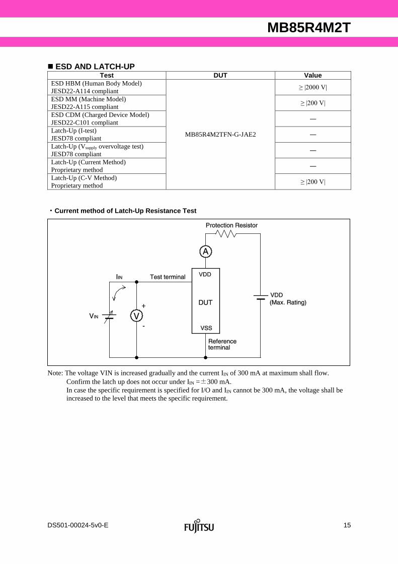
ESD AND LATCH-UP Test DUT Value
ESD HBM (Human Body Model) JESD22-A114 compliant
MB85R4M2TFN-G-JAE2
≥ |2000 V|
ESD MM (Machine Model) JESD22-A115 compliant ≥ |200 V|
ESD CDM (Charged Device Model) JESD22-C101 compliant ―
Latch-Up (I-test) JESD78 compliant ―
Latch-Up (Vsupply overvoltage test) JESD78 compliant ―
Latch-Up (Current Method) Proprietary method ―
Latch-Up (C-V Method) Proprietary method ≥ |200 V|
・Current method of Latch-Up Resistance Test Note: The voltage VIN is increased gradually and the current IIN of 300 mA at maximum shall flow.
Confirm the latch up does not occur under IIN =±300 mA. In case the specific requirement is specified for I/O and IIN cannot be 300 mA, the voltage shall be increased to the level that meets the specific requirement.

16 DS501-00024-5v0-E
MB85R4M2T
・C-V method of Latch-Up Resistance Test Note: Charge voltage alternately switching 1 and 2 approximately 2 sec intervals. This switching process is
considered as one cycle. Repeat this process 5 times. However, if the latch-up condition occurs before completing 5times, this test must be stopped immediately.
REFLOW CONDITIONS AND FLOOR LIFE [ JEDEC MSL ] : Moisture Sensitivity Level 3 (ISP/JEDEC J-STD-020D)
CURRENT STATUS ON CONTAINED RESTRICTED SUBSTANCES This product complies with the regulations of REACH Regulations, EU RoHS Directive and China RoHS.

DS501-00024-5v0-E 17
MB85R4M2T
ORDERING INFORMATION
Part Number Package Shipping form Minimum shipping quantity
MB85R4M2TFN-G-JAE2 44-pin plastic TSOP (FPT-44P-M35) Tray ―*
*: Please contact our sales office about minimum shipping quantity.

18 DS501-00024-5v0-E
MB85R4M2T
PACKAGE DIMENSIONS
44-pin plastic TSOP Lead pitch
Package width ×package length 10.16 × 18.41mm
Lead shape
Sealing method
Mounting height
FPT-44P-M35 / MB85R4M2T
Dimensions in mm.
0.8mm
Gullwing
Plastic mold
1.2mm
44-pin plastic TSOP(FPT-44P-M35)
Note 1) *1: These dimensions do not include resin protrusion.Note 2) *2: These dimensions do not include tie bar cutting remainder.Pins width and pins thickness include plating thickness.
[44] [23]
LEAD No. [1] [22]
INDEX
0.80TYP
1.20
MA
X
0.05
MIN
0.10 MAX
10.1
6±0.
10
*110
.16±
0.10
11.7
6±0.
20
0.10~0.21
0.25TYP0~8°
0.50
±0.1
5*1 18.41±0.10
*2 0.25~0.40

DS501-00024-5v0-E 19
MB85R4M2T
MARKING
[MB85R4M2TFN-G-JAE2]
[FPT-44P-M35]

20 DS501-00024-5v0-E
MB85R4M2T
PACKING 1. Tray
1.1 Tray dimensions
PKG code Maximum storage capacity pcs/tray pcs/inner box pcs/outer box
FPT-44P-M35 126 1260 (10trays)
5040 (4 inner boxes, Max)
FPT44
.
Dimensions in mm. Material: Conductive-Polyphenyleneether(PPE)
Heat resistance temperature: 150℃(max)

DS501-00024-5v0-E 21
MB85R4M2T
1.2 IC orientation
1.3 Product label indicators Label I: Label on Inner box/Moisture Barrier Bag/ (It sticks it on the reel for the emboss taping) [C-3 Label (50mm x 100mm) Supplemental Label (20mm x 100mm)]
(Customer part number or FJ part number)
(Customer part number or FJ part number)
(FJ control number bar code)XX/XX XXXX-XXX XXX
XXXX-XXX XXX(Lot Number and quantity)
(Package count)
(Customer part number or FJ part numberbar code)
(Part number and quantity)
(FJ control number)
QC PASS
XXXXXXXXXXXXXX
XXXX/XX/XX (Packed years/month/day) ASSEMBLED IN xxxx
(3N)1 XXXXXXXXXXXXXX XXX
(Quantity)
(3N)2 XXXXXXXXXX
XXX pcs
XXXXXX
XXXXXXXXXXXXXX
(Customer part number or FJ part number)XXXXXXXXXXXXXX
(Comment)XXXXXXXXXXXXXX(FJ control number )XXXXXXXXXX
(LEAD FREE mark)
C3-Label
Perforated line
Supplemental Label

22 DS501-00024-5v0-E
MB85R4M2T
1.4 Dimensions for container (1) Dimensions for inner box L W H 162 360 90
(Dimensions in mm) (2) Dimensions for outer box
L W H 410 375 225
(Dimensions in mm)
L
W
H
L
W
H

DS501-00024-5v0-E 23
MB85R4M2T
MAJOR CHANGES IN THIS EDITION A change on a page is indicated by a vertical line drawn on the left side of that page.
Page Section Change Results 1 2 17 18 19
FEATURES PIN ASSINGMENTS ORDERING INFORMATION PACKAGE DIMENSION MARKING
Package code is changed. Part Number is changed. Marking is changed.
5 FUNCTONAL TRUTH TABLE OF BYTE CONTROL
Following comment is added. In writing, please don’t switch /LB and/or /UB during /CE=”L”.
8 ELECTRICAL CHARACTERISTICS 2. AC Characteristics
tOH and tOAH are redefined. tOH: /CE Output Data Hold time tOAH: Address Access Output Output Data Hold time
20 PACKING Packing information is added.

FUJITSU SEMICONDUCTOR LIMITED Shin-Yokohama Chuo Building, 2-100-45 Shin-Yokohama, Kohoku-ku, Yokohama, Kanagawa 222-0033, Japan http://jp.fujitsu.com/fsl/en/
All Rights Reserved. FUJITSU SEMICONDUCTOR LIMITED, its subsidiaries and affiliates (collectively, "FUJITSU SEMICONDUCTOR") reserves the right to make changes to the information contained in this document without notice. Please contact your FUJITSU SEMICONDUCTOR sales representatives before order of FUJITSU SEMICONDUCTOR device. Information contained in this document, such as descriptions of function and application circuit examples is presented solely for reference to examples of operations and uses of FUJITSU SEMICONDUCTOR device. FUJITSU SEMICONDUCTOR disclaims any and all warranties of any kind, whether express or implied, related to such information, including, without limitation, quality, accuracy, performance, proper operation of the device or non-infringement. If you develop equipment or product incorporating the FUJITSU SEMICONDUCTOR device based on such information, you must assume any responsibility or liability arising out of or in connection with such information or any use thereof. FUJITSU SEMICONDUCTOR assumes no responsibility or liability for any damages whatsoever arising out of or in connection with such information or any use thereof. Nothing contained in this document shall be construed as granting or conferring any right under any patents, copyrights, or any other intellectual property rights of FUJITSU SEMICONDUCTOR or any third party by license or otherwise, express or implied. FUJITSU SEMICONDUCTOR assumes no responsibility or liability for any infringement of any intellectual property rights or other rights of third parties resulting from or in connection with the information contained herein or use thereof. The products described in this document are designed, developed and manufactured as contemplated for general use including without limitation, ordinary industrial use, general office use, personal use, and household use, but are not designed, developed and manufactured as contemplated (1) for use accompanying fatal risks or dangers that, unless extremely high levels of safety is secured, could lead directly to death, personal injury, severe physical damage or other loss (including, without limitation, use in nuclear facility, aircraft flight control system, air traffic control system, mass transport control system, medical life support system and military application), or (2) for use requiring extremely high level of reliability (including, without limitation, submersible repeater and artificial satellite). FUJITSU SEMICONDUCTOR shall not be liable for you and/or any third party for any claims or damages arising out of or in connection with above-mentioned uses of the products. Any semiconductor devices fail or malfunction with some probability. You are responsible for providing adequate designs and safeguards against injury, damage or loss from such failures or malfunctions, by incorporating safety design measures into your facility, equipments and products such as redundancy, fire protection, and prevention of overcurrent levels and other abnormal operating conditions. The products and technical information described in this document are subject to the Foreign Exchange and Foreign Trade Control Law of Japan, and may be subject to export or import laws or regulations in U.S. or other countries. You are responsible for ensuring compliance with such laws and regulations relating to export or re-export of the products and technical information described herein. All company names, brand names and trademarks herein are property of their respective owners.
Edited: System Memory Company
MB85R4M2T