Embed Size (px)
Citation preview
1
4. Integrated Photonics (or optoelectronics on a flatland)

Benefits of 𝒊𝒏𝒕𝒆𝒈𝒓𝒂𝒕𝒊𝒐𝒏𝒙
−∞
in Electronics:
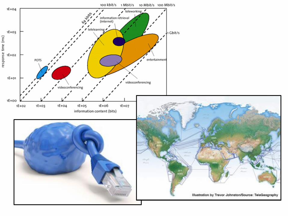
4
Mach-Zehnder modulator made from Indium Phosphide (InP) designed for 128 Gbs.
Are we experiencing a
similar transformation in Photonics ?
5
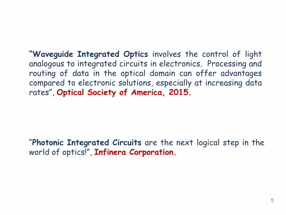
“Photonic Integrated Circuits are the next logical step in the world of optics!”, Infinera Corporation.
“Waveguide Integrated Optics involves the control of light analogous to integrated circuits in electronics. Processing and routing of data in the optical domain can offer advantages compared to electronic solutions, especially at increasing data rates”, Optical Society of America, 2015.

6
lasers photodetectors
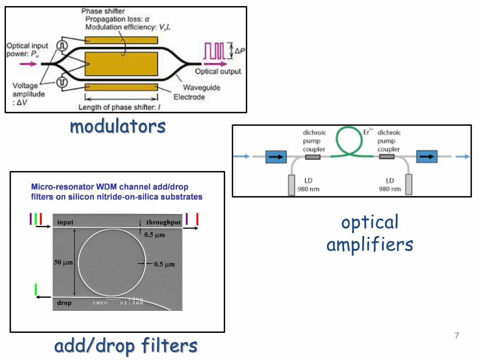
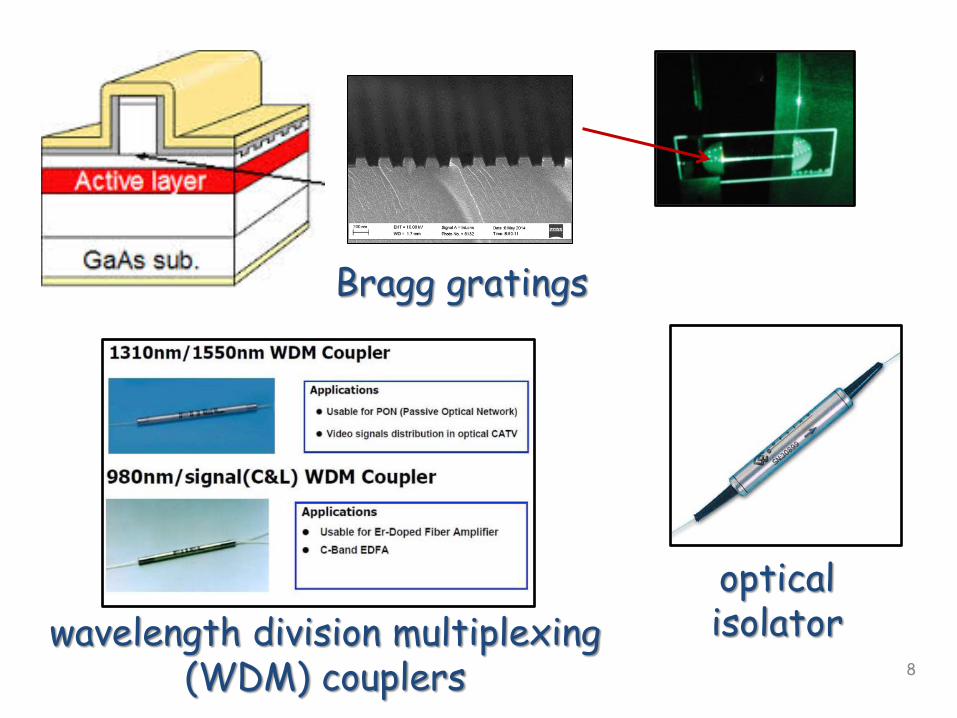
A Few Examples of Integrated Photonic Components
optical fibers planar waveguides
7
modulators
add/drop filters
optical amplifiers
8
wavelength division multiplexing (WDM) couplers
optical isolator
Bragg gratings

9
M. Liu et al., Nature 474, 64 (2011)
A graphene-based electro-absorption modulator: In a device such as the one demonstrated by Liu et al. in 2011, electrically connected graphene is coupled to a SiO2
waveguide carrying a CW photon stream.
Driving Fundamental Research on Novel Materials and Devices

Early Days …
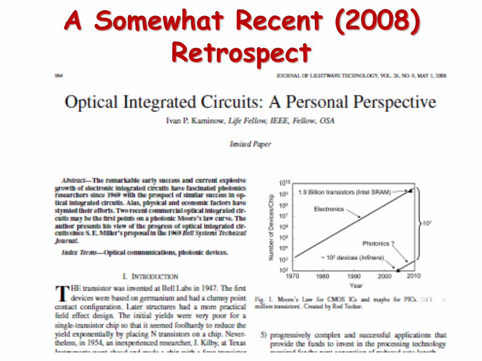
A Somewhat Recent (2008) Retrospect

A Crucial Element: Light Guiding Geometries
2D (slab) and 3D (channel & optical fiber)
𝑛𝑓 > 𝑛𝑐
𝑛𝑓 > 𝑛𝑠
graded refractive index
step refractive index
𝑇 > 𝑡0
Requirements
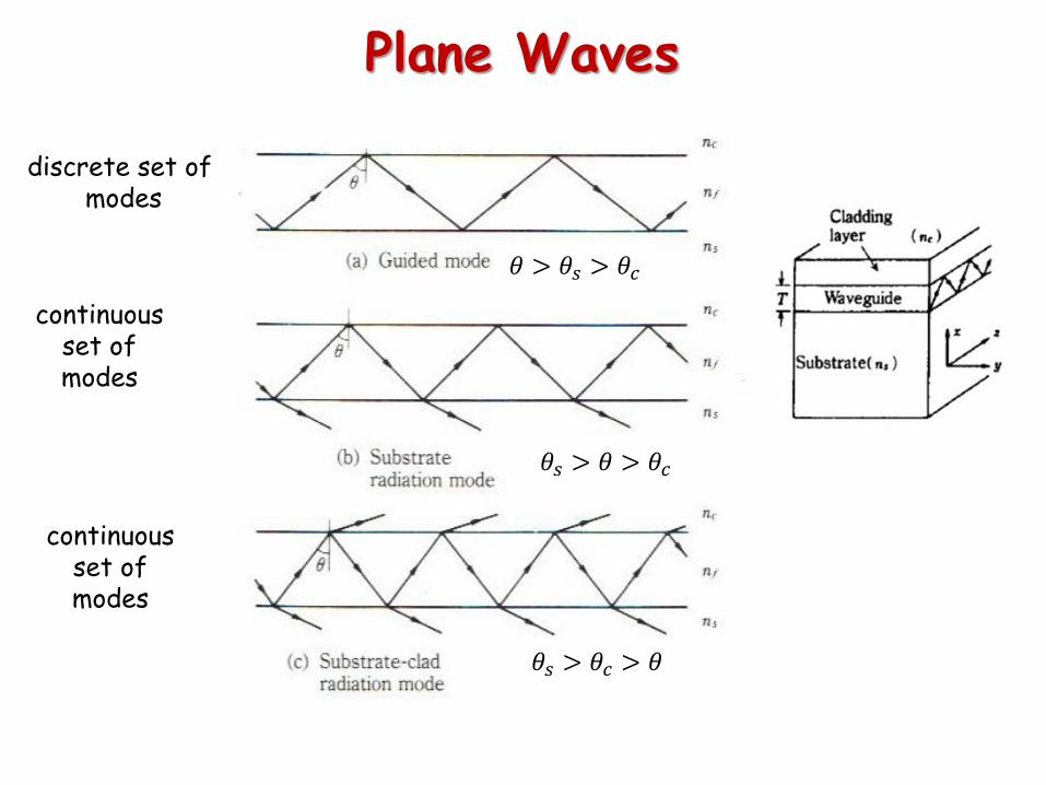
Plane Waves
discrete set of modes
continuous set of modes
continuous set of modes
𝜃𝑠 > 𝜃 > 𝜃𝑐
𝜃 > 𝜃𝑠 > 𝜃𝑐
𝜃𝑠 > 𝜃𝑐 > 𝜃
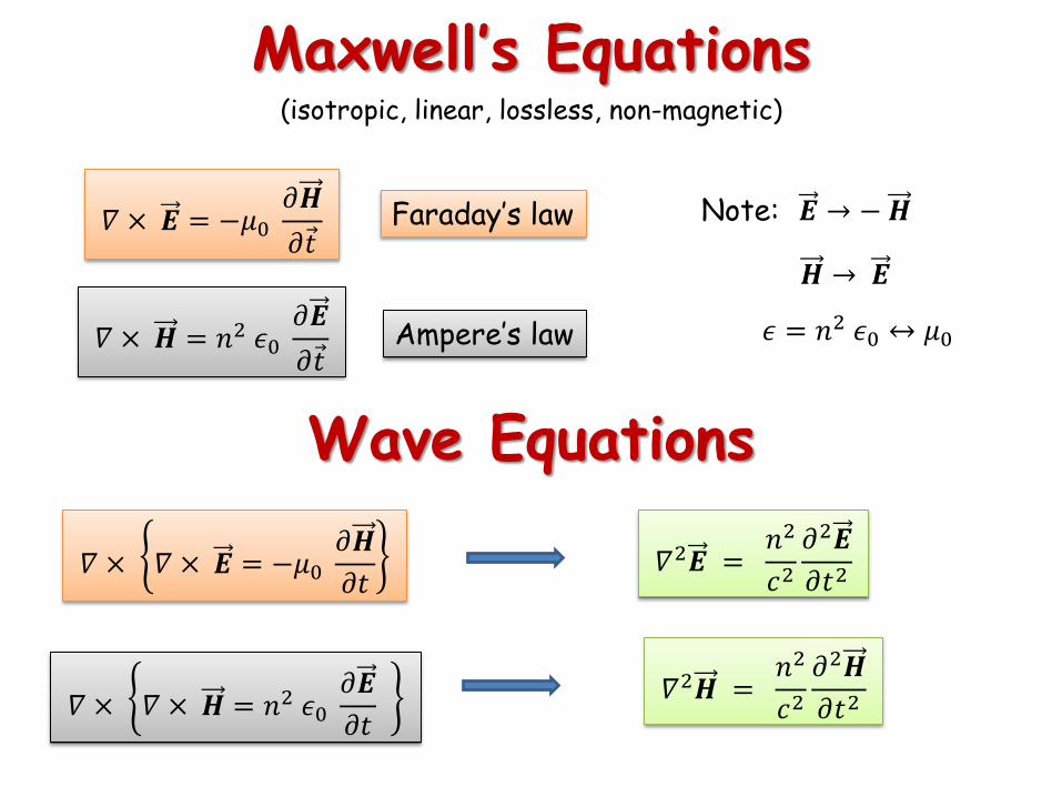
Maxwell’s Equations (isotropic, linear, lossless, non-magnetic)
𝛻 × 𝑬 = −𝜇0 𝜕𝑯
𝜕𝑡
𝛻 × 𝑯 = 𝑛2 𝜖0 𝜕𝑬
𝜕𝑡
Faraday’s law
Ampere’s law
𝑬 → − 𝑯
𝑯 → 𝑬
Note:
𝜖 = 𝑛2 𝜖0 ↔ 𝜇0
𝛻 × 𝛻 × 𝑬 = −𝜇0 𝜕𝑯
𝜕𝑡
𝛻 × 𝛻 × 𝑯 = 𝑛2 𝜖0 𝜕𝑬
𝜕𝑡
𝛻2𝑬 = 𝑛2
𝑐2𝜕2𝑬
𝜕𝑡2
𝛻2𝑯 = 𝑛2
𝑐2𝜕2𝑯
𝜕𝑡2
Wave Equations
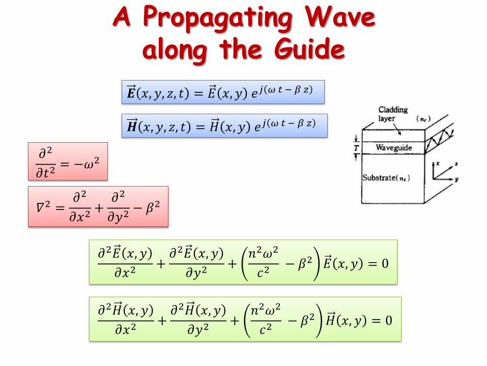
A Propagating Wave along the Guide
𝑬 𝑥, 𝑦, 𝑧, 𝑡 = 𝐸 𝑥, 𝑦 𝑒𝑗 𝜔 𝑡 − 𝛽 𝑧
𝑯 𝑥, 𝑦, 𝑧, 𝑡 = 𝐻 𝑥, 𝑦 𝑒𝑗 𝜔 𝑡 − 𝛽 𝑧
𝜕2
𝜕𝑡2= −𝜔2
𝛻2 =𝜕2
𝜕𝑥2+𝜕2
𝜕𝑦2− 𝛽2
𝜕2𝐸 𝑥, 𝑦
𝜕𝑥2+𝜕2𝐸 𝑥, 𝑦
𝜕𝑦2+𝑛2𝜔2
𝑐2 − 𝛽2 𝐸 𝑥, 𝑦 = 0
𝜕2𝐻 𝑥, 𝑦
𝜕𝑥2+𝜕2𝐻 𝑥, 𝑦
𝜕𝑦2+𝑛2𝜔2
𝑐2 − 𝛽2 𝐻 𝑥, 𝑦 = 0
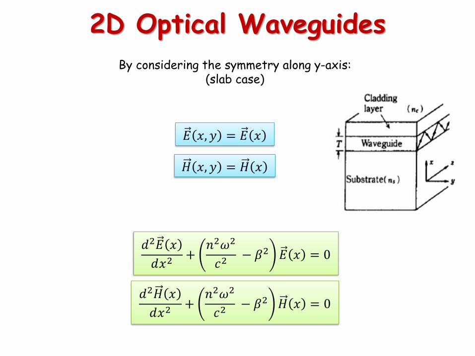
2D Optical Waveguides
By considering the symmetry along y-axis: (slab case)
𝐸 𝑥, 𝑦 = 𝐸 𝑥
𝐻 𝑥, 𝑦 = 𝐻 𝑥
𝑑2𝐸 𝑥
𝑑𝑥2+𝑛2𝜔2
𝑐2 − 𝛽2 𝐸 𝑥 = 0
𝑑2𝐻 𝑥
𝑑𝑥2+𝑛2𝜔2
𝑐2 − 𝛽2 𝐻 𝑥 = 0
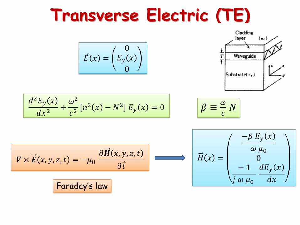
Transverse Electric (TE)
𝐸 𝑥 =0𝐸𝑦 𝑥
0
𝛻 × 𝑬 𝑥, 𝑦, 𝑧, 𝑡 = −𝜇0 𝜕𝑯 𝑥, 𝑦, 𝑧, 𝑡
𝜕𝑡 𝐻 𝑥 =
−𝛽 𝐸𝑦 𝑥
𝜔 𝜇00
− 1
𝑗 𝜔 𝜇0 𝑑𝐸𝑦 𝑥
𝑑𝑥
Faraday’s law
𝛽 ≡𝜔
𝑐 𝑁
𝑑2𝐸𝑦 𝑥
𝑑𝑥2+𝜔2
𝑐2𝑛2 𝑥 − 𝑁2 𝐸𝑦 𝑥 = 0
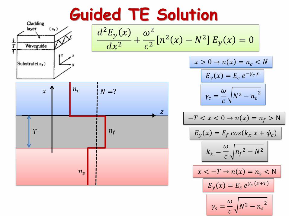
Guided TE Solution 𝑑2𝐸𝑦 𝑥
𝑑𝑥2+𝜔2
𝑐2𝑛2 𝑥 − 𝑁2 𝐸𝑦 𝑥 = 0
𝑥
𝑧
𝑁 =?
𝑛𝑠
𝑛𝑓
𝑛𝑐
𝑥 > 0 → 𝑛 𝑥 = 𝑛𝑐 < 𝑁
−𝑇 < 𝑥 < 0 → 𝑛 𝑥 = 𝑛𝑓 > N
𝑥 < −𝑇 → 𝑛 𝑥 = 𝑛𝑠 < N
𝐸𝑦 𝑥 = 𝐸𝑐 𝑒−𝛾𝑐 𝑥
𝐸𝑦 𝑥 = 𝐸𝑠 𝑒𝛾𝑠 𝑥+𝑇
𝑇
𝛾𝑐 =𝜔
𝑐𝑁2 − 𝑛𝑐
2
𝛾𝑠 =𝜔
𝑐𝑁2 − 𝑛𝑠
2
𝐸𝑦 𝑥 = 𝐸𝑓 𝑐𝑜𝑠 𝑘𝑥 𝑥 + 𝜙𝑐
𝑘𝑥 =𝜔
𝑐𝑛𝑓2 − 𝑁2
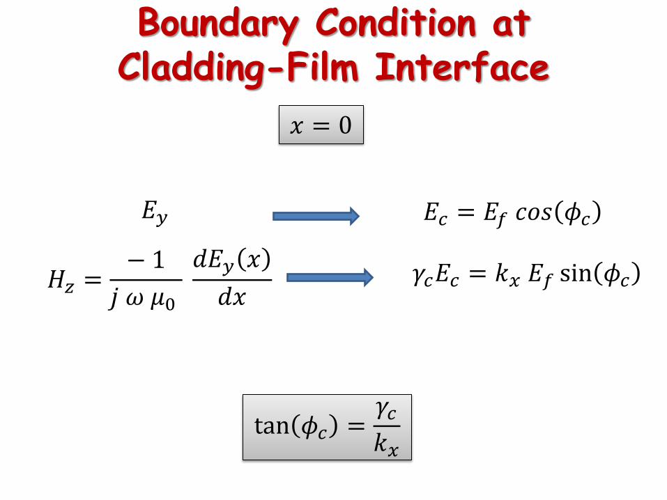
Boundary Condition at Cladding-Film Interface
𝐸𝑐 = 𝐸𝑓 𝑐𝑜𝑠 𝜙𝑐
𝑥 = 0
𝐸𝑦
𝐻𝑧 =− 1
𝑗 𝜔 𝜇0 𝑑𝐸𝑦 𝑥
𝑑𝑥 𝛾𝑐𝐸𝑐 = 𝑘𝑥 𝐸𝑓 sin 𝜙𝑐
tan 𝜙𝑐 =𝛾𝑐𝑘𝑥
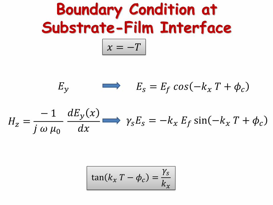
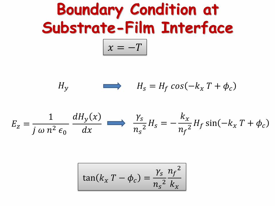
Boundary Condition at Substrate-Film Interface
𝐸𝑠 = 𝐸𝑓 𝑐𝑜𝑠 −𝑘𝑥 𝑇 + 𝜙𝑐
𝑥 = −𝑇
𝐸𝑦
𝐻𝑧 =− 1
𝑗 𝜔 𝜇0 𝑑𝐸𝑦 𝑥
𝑑𝑥 𝛾𝑠𝐸𝑠 = −𝑘𝑥 𝐸𝑓 sin −𝑘𝑥 𝑇 + 𝜙𝑐
tan 𝑘𝑥 𝑇 − 𝜙𝑐 =𝛾𝑠𝑘𝑥
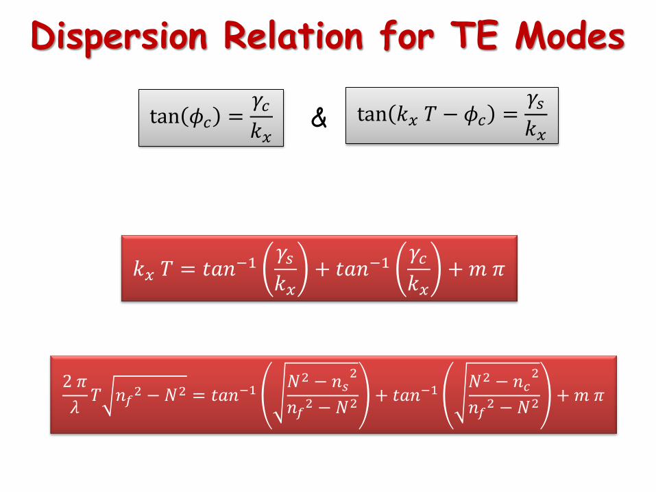
Dispersion Relation for TE Modes
tan 𝜙𝑐 =𝛾𝑐𝑘𝑥
tan 𝑘𝑥 𝑇 − 𝜙𝑐 =𝛾𝑠𝑘𝑥
𝑘𝑥 𝑇 = 𝑡𝑎𝑛−1𝛾𝑠𝑘𝑥+ 𝑡𝑎𝑛−1
𝛾𝑐𝑘𝑥+𝑚 𝜋
&
2 𝜋
𝜆𝑇 𝑛𝑓
2 − 𝑁2 = 𝑡𝑎𝑛−1𝑁2 − 𝑛𝑠
2
𝑛𝑓2 − 𝑁2
+ 𝑡𝑎𝑛−1𝑁2 − 𝑛𝑐
2
𝑛𝑓2 − 𝑁2
+𝑚 𝜋
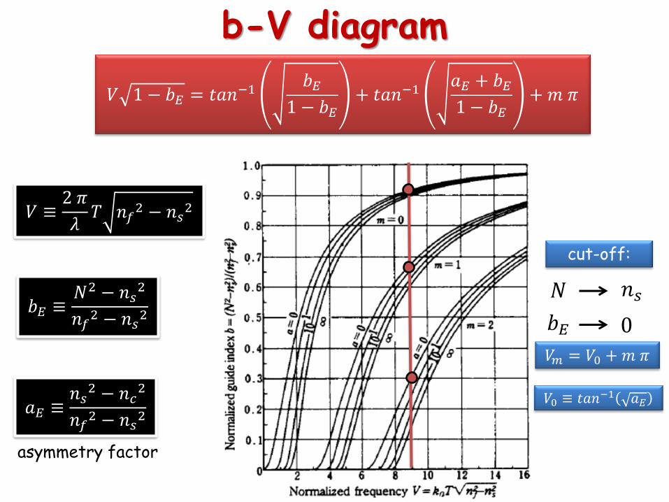
b-V diagram
2 𝜋
𝜆𝑇 𝑛𝑓
2 − 𝑁2
𝑉 ≡2 𝜋
𝜆𝑇 𝑛𝑓
2 − 𝑛𝑠2
𝑏𝐸 ≡𝑁2 − 𝑛𝑠
2
𝑛𝑓2 − 𝑛𝑠
2
𝑎𝐸 ≡𝑛𝑠2 − 𝑛𝑐
2
𝑛𝑓2 − 𝑛𝑠
2
𝑉 1 − 𝑏𝐸 = 𝑡𝑎𝑛−1
𝑏𝐸1 − 𝑏𝐸
+ 𝑡𝑎𝑛−1𝑎𝐸 + 𝑏𝐸1 − 𝑏𝐸
+𝑚 𝜋
cut-off:
𝑁 𝑛𝑠
0 𝑏𝐸
𝑉𝑚 = 𝑉0 +𝑚 𝜋
𝑉0 ≡ 𝑡𝑎𝑛−1 𝑎𝐸
asymmetry factor
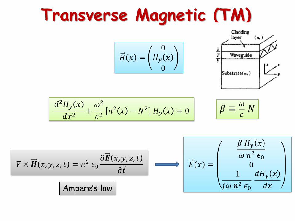
Transverse Magnetic (TM)
𝐻 𝑥 =0𝐻𝑦 𝑥
0
𝛻 × 𝑯 𝑥, 𝑦, 𝑧, 𝑡 = 𝑛2 𝜖0𝜕𝑬 𝑥, 𝑦, 𝑧, 𝑡
𝜕𝑡 𝐸 𝑥 =
𝛽 𝐻𝑦 𝑥
𝜔 𝑛2 𝜖00
1
𝑗𝜔 𝑛2 𝜖0 𝑑𝐻𝑦 𝑥
𝑑𝑥
Ampere’s law
𝑑2𝐻𝑦 𝑥
𝑑𝑥2+𝜔2
𝑐2𝑛2 𝑥 − 𝑁2 𝐻𝑦 𝑥 = 0 𝛽 ≡
𝜔
𝑐 𝑁
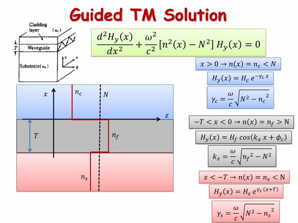
Guided TM Solution 𝑑2𝐻𝑦 𝑥
𝑑𝑥2+𝜔2
𝑐2𝑛2 𝑥 − 𝑁2 𝐻𝑦 𝑥 = 0
𝑥
𝑧
𝑁
𝑛𝑠
𝑛𝑓
𝑛𝑐
𝑥 > 0 → 𝑛 𝑥 = 𝑛𝑐 < 𝑁
−𝑇 < 𝑥 < 0 → 𝑛 𝑥 = 𝑛𝑓 > N
𝑥 < −𝑇 → 𝑛 𝑥 = 𝑛𝑠 < N
𝐻𝑦 𝑥 = 𝐻𝑐 𝑒−𝛾𝑐 𝑥
𝐻𝑦 𝑥 = 𝐻𝑠 𝑒𝛾𝑠 𝑥+𝑇
𝑇
𝛾𝑐 =𝜔
𝑐𝑁2 − 𝑛𝑐
2
𝛾𝑠 =𝜔
𝑐𝑁2 − 𝑛𝑠
2
𝐻𝑦 𝑥 = 𝐻𝑓 𝑐𝑜𝑠 𝑘𝑥 𝑥 + 𝜙𝑐
𝑘𝑥 =𝜔
𝑐𝑛𝑓2 − 𝑁2

Boundary Condition at Cladding-Film Interface
𝐻𝑐 = 𝐻𝑓 𝑐𝑜𝑠 𝜙𝑐
𝑥 = 0
𝐻𝑦
𝛾𝑐𝑛𝑐2𝐻𝑐 =𝑘𝑥𝑛𝑓2 𝐻𝑓 sin 𝜙𝑐
tan 𝜙𝑐 =𝛾𝑐𝑛𝑐2
𝑛𝑓2
𝑘𝑥
𝐸𝑧 =1
𝑗 𝜔 𝑛2 𝜖0 𝑑𝐻𝑦 𝑥
𝑑𝑥
Boundary Condition at Substrate-Film Interface
𝐻𝑠 = 𝐻𝑓 𝑐𝑜𝑠 −𝑘𝑥 𝑇 + 𝜙𝑐
𝑥 = −𝑇
𝐻𝑦
𝐸𝑧 =1
𝑗 𝜔 𝑛2 𝜖0 𝑑𝐻𝑦 𝑥
𝑑𝑥
𝛾𝑠𝑛𝑠2𝐻𝑠 = −
𝑘𝑥𝑛𝑓2𝐻𝑓 sin −𝑘𝑥 𝑇 + 𝜙𝑐
tan 𝑘𝑥 𝑇 − 𝜙𝑐 =𝛾𝑠𝑛𝑠2
𝑛𝑓2
𝑘𝑥
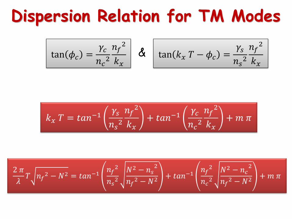
Dispersion Relation for TM Modes
𝑘𝑥 𝑇 = 𝑡𝑎𝑛−1𝛾𝑠𝑛𝑠2
𝑛𝑓2
𝑘𝑥+ 𝑡𝑎𝑛−1
𝛾𝑐𝑛𝑐2
𝑛𝑓2
𝑘𝑥+𝑚 𝜋
&
2 𝜋
𝜆𝑇 𝑛𝑓
2 − 𝑁2 = 𝑡𝑎𝑛−1𝑛𝑓2
𝑛𝑠2
𝑁2 − 𝑛𝑠2
𝑛𝑓2 − 𝑁2
+ 𝑡𝑎𝑛−1𝑛𝑓2
𝑛𝑐2
𝑁2 − 𝑛𝑐2
𝑛𝑓2 − 𝑁2
+𝑚 𝜋
tan 𝜙𝑐 =𝛾𝑐𝑛𝑐2
𝑛𝑓2
𝑘𝑥 tan 𝑘𝑥 𝑇 − 𝜙𝑐 =
𝛾𝑠𝑛𝑠2
𝑛𝑓2
𝑘𝑥
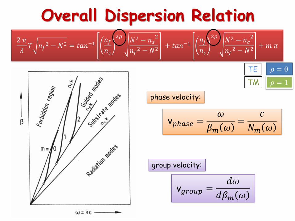
Overall Dispersion Relation 2 𝜋
𝜆𝑇 𝑛𝑓
2 − 𝑁2 = 𝑡𝑎𝑛−1𝑛𝑓
𝑛𝑠
2𝜌𝑁2 − 𝑛𝑠
2
𝑛𝑓2 − 𝑁2
+ 𝑡𝑎𝑛−1𝑛𝑓
𝑛𝑐
2𝜌𝑁2 − 𝑛𝑐
2
𝑛𝑓2 − 𝑁2
+𝑚 𝜋
𝜌 = 0
𝜌 = 1
TE
TM
v𝑔𝑟𝑜𝑢𝑝 =𝑑𝜔
𝑑𝛽𝑚 𝜔
phase velocity:
group velocity:
v𝑝ℎ𝑎𝑠𝑒 =𝜔
𝛽𝑚 𝜔=𝑐
𝑁𝑚 𝜔
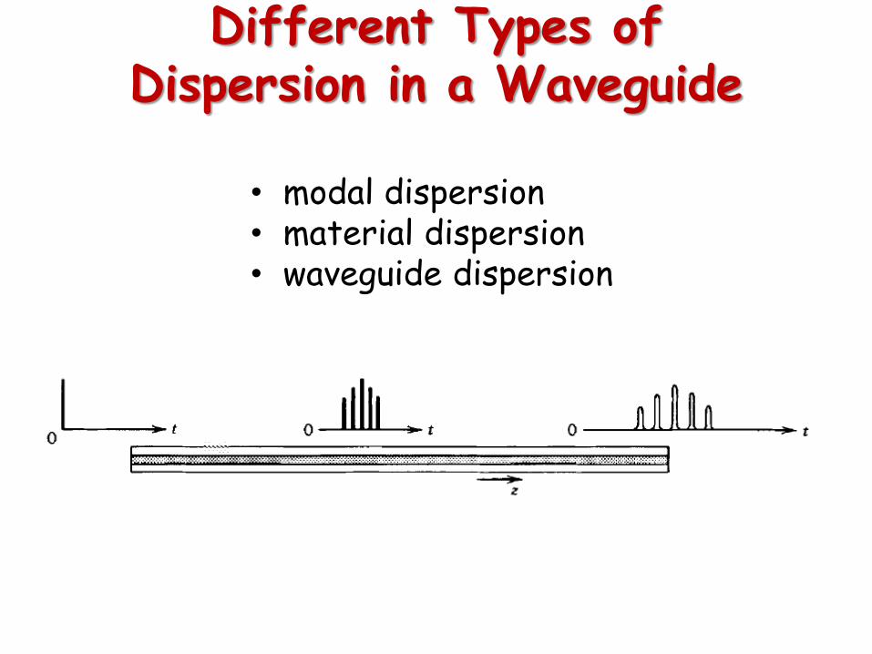
Different Types of Dispersion in a Waveguide
• modal dispersion • material dispersion • waveguide dispersion
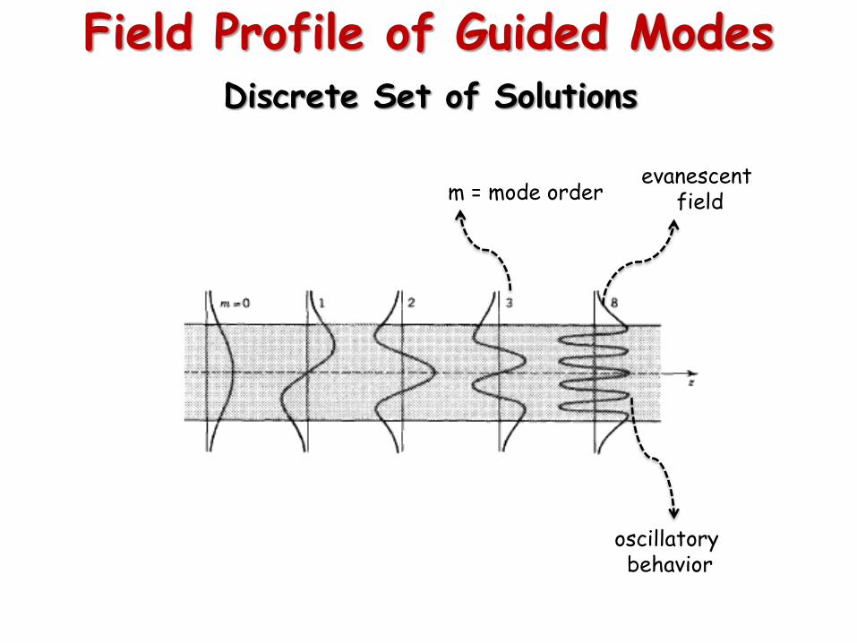
Field Profile of Guided Modes Discrete Set of Solutions
evanescent field
oscillatory behavior
m = mode order

Propagating Power along the Waveguide
𝑆 = 1
2Re 𝐸 × 𝐻∗ 𝑃𝑧 =
1
2𝑆𝑧 𝑑𝑥
∞
−∞
Power/unit-width:
TE mode:
𝑃𝑧 = −1
2𝐸𝑦 𝐻𝑥
∗𝑑𝑥∞
−∞
𝐻𝑥 =−𝛽 𝐸𝑦 𝑥
𝜔 𝜇0
𝑃𝑧 =𝛽
2 𝜔 𝜇0 𝐸𝑦
2 𝑑𝑥
∞
−∞
Poynting vector:
𝑃𝑧 =𝛽
2 𝜔 𝜇0 𝐸𝑦
2 𝑑𝑥
∞
−∞=𝛽
4 𝜔 𝜇0𝐸𝑓2 𝑇𝑒𝑓𝑓
𝑇𝑒𝑓𝑓 ≡ 𝑇 + 𝜆
2𝜋 𝑁2 − 𝑛𝑠2
+𝜆
2𝜋 𝑁2 − 𝑛𝑐2
effective thickness or mode size wavelength dependent
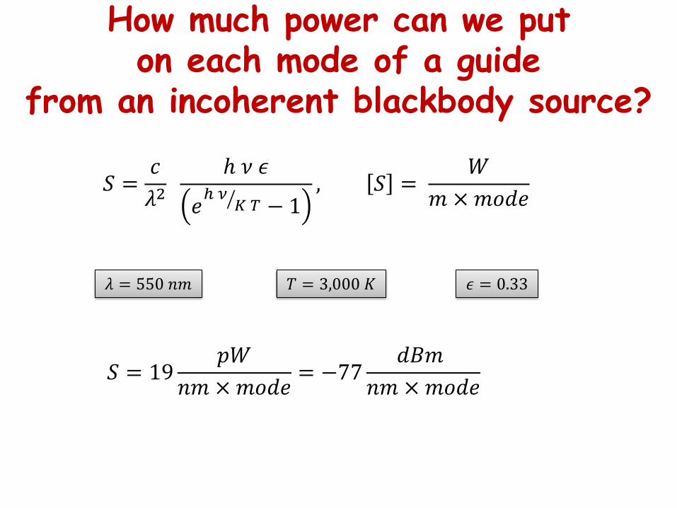
How much power can we put on each mode of a guide
from an incoherent blackbody source?
𝑆 =𝑐
𝜆2 ℎ 𝜈 𝜖
𝑒ℎ 𝜈𝐾 𝑇 − 1
, 𝑆 = 𝑊
𝑚 ×𝑚𝑜𝑑𝑒
𝑆 = 19𝑝𝑊
𝑛𝑚 ×𝑚𝑜𝑑𝑒= −77
𝑑𝐵𝑚
𝑛𝑚 ×𝑚𝑜𝑑𝑒
𝜆 = 550 𝑛𝑚 𝑇 = 3,000 𝐾 𝜖 = 0.33
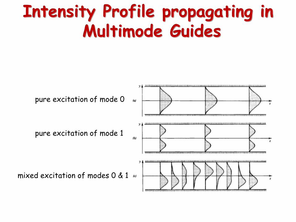
Intensity Profile propagating in Multimode Guides
pure excitation of mode 0
pure excitation of mode 1
mixed excitation of modes 0 & 1
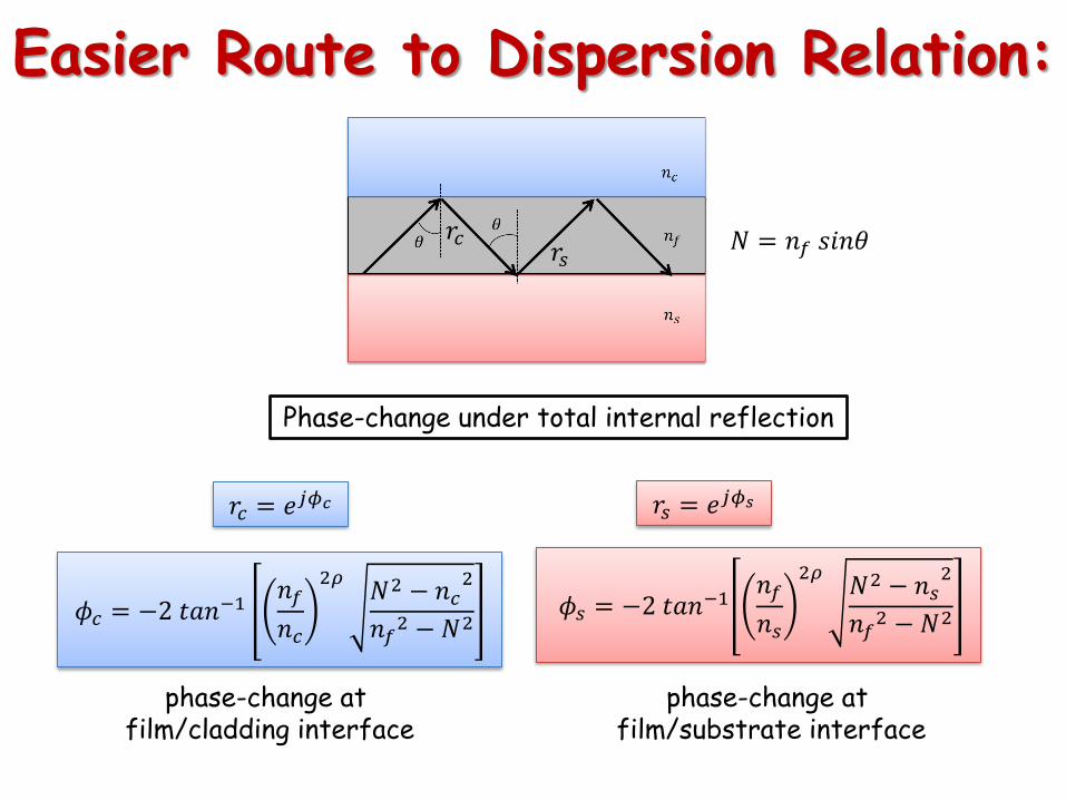
Easier Route to Dispersion Relation:
Phase-change under total internal reflection
𝑟𝑐 = 𝑒𝑗𝜙𝑐
𝑟𝑐 𝑟𝑠
phase-change at film/substrate interface
phase-change at film/cladding interface
𝜙𝑐 = −2 𝑡𝑎𝑛−1𝑛𝑓
𝑛𝑐
2𝜌𝑁2 − 𝑛𝑐
2
𝑛𝑓2 − 𝑁2
𝑟𝑠 = 𝑒𝑗𝜙𝑠
𝜙𝑠 = −2 𝑡𝑎𝑛−1𝑛𝑓
𝑛𝑠
2𝜌𝑁2 − 𝑛𝑠
2
𝑛𝑓2 − 𝑁2
𝑁 = 𝑛𝑓 𝑠𝑖𝑛𝜃
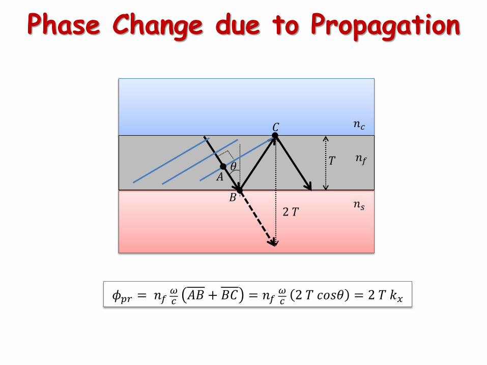
Phase Change due to Propagation
𝜙𝑝𝑟 = 𝑛𝑓 𝜔𝑐 𝐴𝐵 + 𝐵𝐶 = 𝑛𝑓
𝜔𝑐 2 𝑇 𝑐𝑜𝑠𝜃 = 2 𝑇 𝑘𝑥
𝑛𝑠
𝑛𝑐
𝑛𝑓 𝜃 𝐴
𝐶
𝐵
𝑇
2 𝑇

Resonant Condition:
𝜙𝑝𝑟 +𝜙𝑠 + 𝜙𝑐 = 2 𝜋 𝑚
2 𝑘𝑥𝑇 − 2 𝑡𝑎𝑛−1𝑛𝑓
𝑛𝑠
2𝜌𝑁2 − 𝑛𝑠
2
𝑛𝑓2 − 𝑁2
−2 𝑡𝑎𝑛−1𝑛𝑓
𝑛𝑐
2𝜌𝑁2 − 𝑛𝑐
2
𝑛𝑓2 − 𝑁2
= 2 𝜋 𝑚
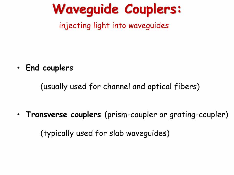
Waveguide Couplers: injecting light into waveguides
• End couplers (usually used for channel and optical fibers)
• Transverse couplers (prism-coupler or grating-coupler) (typically used for slab waveguides)
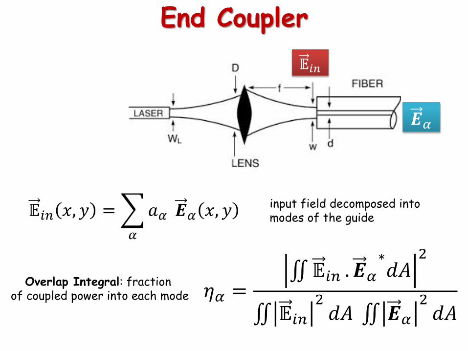
End Coupler
𝔼𝑖𝑛 𝑥, 𝑦 = 𝑎𝛼
𝛼
𝑬𝛼 𝑥, 𝑦
𝜂𝛼 = 𝔼𝑖𝑛 . 𝑬𝛼
∗𝑑𝐴2
𝔼𝑖𝑛2𝑑𝐴 𝑬𝛼
2𝑑𝐴
𝔼𝑖𝑛
𝑬𝛼
input field decomposed into modes of the guide
Overlap Integral: fraction of coupled power into each mode
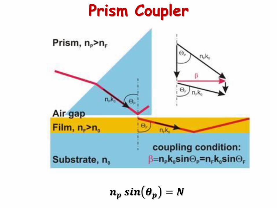
Prism Coupler
𝒏𝒑 𝒔𝒊𝒏 𝜽𝒑 = 𝑵
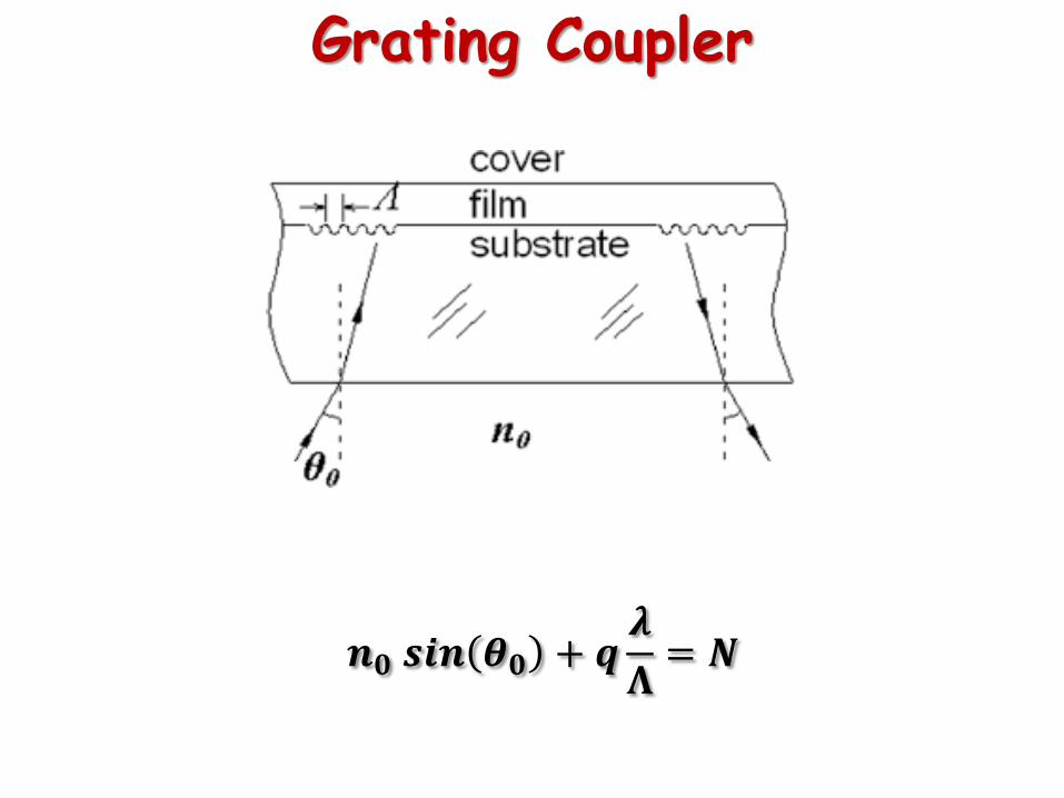
Grating Coupler
𝒏𝟎 𝒔𝒊𝒏 𝜽𝟎 + 𝒒𝝀
𝚲= 𝑵