Embed Size (px)
Citation preview

University of KentuckyUKnowledge
Mechanical Engineering Faculty Patents Mechanical Engineering
4-27-2010
Plasma ActuatorJamey D. JacobUniversity of Kentucky
Right click to open a feedback form in a new tab to let us know how this document benefits you.
Follow this and additional works at: https://uknowledge.uky.edu/me_patents
Part of the Mechanical Engineering Commons
This Patent is brought to you for free and open access by the Mechanical Engineering at UKnowledge. It has been accepted for inclusion in MechanicalEngineering Faculty Patents by an authorized administrator of UKnowledge. For more information, please contact [email protected].
Recommended CitationJacob, Jamey D., "Plasma Actuator" (2010). Mechanical Engineering Faculty Patents. 15.https://uknowledge.uky.edu/me_patents/15

US007703479B2
(12) Ulllted States Patent (10) Patent N0.: US 7,703,479 B2 Jacob (45) Date of Patent: Apr. 27, 2010
(54) PLASMA ACTUATOR 5,894,990 A 4/1999 GleZer et al.
' 5,921,757 A 7/1999 Tsutsuiet a1.
(75) Inventor: Jamey D. Jacob, St1llWater, OK (US) 5,988,522 A 11/1999 Glezer et a1‘
(73) Assignee: The University of Kentucky Research 6’056’204 A 5/2000 Glezer et a1‘ Foundation’ Lexington’ KY (Us) 6,123,145 A 9/2000 GleZer et al.
6,315,216 B1 11/2001 Boecking ( * ) Notice: Subject to any disclaimer, the term ofthis 6,431,112 B1 * 8/2002 Sill et al. ............... .. 118/723 E
patent is extended or adjusted under 35 6,457,654 B1 10/2002 GleZer et a1, U-S-C- 154(1)) by 711 days- 6,474,570 B2 11/2002 Chen
6 540 203 B1 4/2003 H ' tt (21) Appl. No.2 11/581,932 ’ ’ “mm
(22) Filed: Oct. 17, 2006
(65) Prior Publication Data (Continued)
US 2007/0089795 A1 Apr. 26, 2007 FOREIGN PATENT DOCUMENTS
Related US. Application Data JP 61054248 3/1986
(60) Provisional application No. 60/727,364, ?led on Oct. 17, 2005.
(Continued) (51) Int. Cl.
F15C 1/04 (200601) OTHER PUBLICATIONS
(52) US. Cl. ....................... .. 137/828; 417/48; 244/130; “Flow Control Using Plasma Actuators and hear/Annular Plasma 244/207 Synthetic Jet Actuators” by Arvind Santhanakrishnan and Jamey
(58) Field of Classi?cation Search ............... .. 137/ 827, Jacob, published 2006*
137/825, 826, 828; 417/49, 50, 48; 239/690, _ 239/690.l; 361/227, 228; 244/205, 207, (Con?rmed)
S 1, _ ?l f 1 h h, 244/130 Primary Examinerilohn Rivell ee app lcanon e or Comp ete seam lstory' Assistant Examiner4Craig M Schneider
(56) References Cited (74) Attorney, Agent, or FirmiKing & Schickli, PLLC
U.S. PATENT DOCUMENTS
1,773,969 A 8/1930 Dreyfus et al. 3,281,324 A 10/1966 Henins et al. 4,828,184 A 5/1989 Gardner et a1. 5,040,560 A 8/1991 GleZer et al. 5,060,867 A 10/1991 LuXton et al. 5,414,324 A 5/1995 Roth et a1. 5,622,611 A 4/1997 Marks et a1. 5,758,823 A 6/1998 GleZer et al. 5,885,358 A 3/1999 Maydan et a1.
(57) ABSTRACT
An actuator including a ?rst and second conductor on a dielectric, Wherein application of a voltage to the ?rst con ductor creates a plasma, thereby modifying a ?uid How in communication With the actuator. Related systems and meth ods are also provided.
25 Claims, 9 Drawing Sheets

US 7,703,479 B2 Page 2
US. PATENT DOCUMENTS JP 2002069603 3/2002 WO WO9622841 8/1996
6,550,691 B2 4/2003 Pence W0 WO9926457 5/1999 6,570,333 B1* 5/2003 Miller et al. ......... .. 315/111.21 6,619,788 B2 9/2003 Condie OTHER PUBLICATIONS
6’685’l02 Bl 2/2004 Ml et 31' . “Flow control With plasma synthetic jet actuators” by Arvind 6,722,581 B2 4/2004 Saddoughi . . * Santhanakrishnan and Jamey Jacob, published Jan. 19, 2007. 6,848,631 B2 2/2005 Monson et al. . . “ .
Presentation titled Effectiveness of Plasma Actuators as Flow Con 6,872,259 B2 3/2005 Strang . . . ,, . trol Devices in Low Pressure Turbine Blades by Karthik 6,959,471 B2 11/2005 Temple et al. Ramakumar and Jamey Jacob, dated Mar. 7, 2006* 7,380,756 B1 * 6/2008 Enloe et al. ............... .. 244/175 . .
. Jamey D. Jacob and Karthik Ramakumar, Control of Laminar and 2001/0010257 A1 8/2001 N1 et al. . .
Turbulent Shear Flows Using Plasma Actuators, 4th International 2002/0081198 A1 6/2002 Hassan et al. .
Symposium on Turbulence and Shear Flow Phenomena, Jun. 27-29, 2004/0021041 A1 2/2004 Grossman et a1. . .
2005, 6 pgs, Williamsburg, VA. 2005/0074662 A1 4/2005 Cho et al. . . . . .
Ari GleZer and Michael Amitay, Synthetic Jets, Annu. Rev. Fluid 2005/0111185 A1 5/2005 Bhattacharya et al. Mech 2002 503629 Annual Reviews 2005/0127780 A1 6/2005 Ifuku et al. " ’ pp‘ ’ '
FOREIGN PATENT DOCUMENTS
JP 2000208929 7/2000
Martiqua L. Post and Thomas C. Corke, Flow Control With Single Dielectric Barrier Plasma Actuators, 35th Fluid Dynamics Confer ence and Exhibit, Jun. 6, 2005, 19 pgs, Toronto, Canada.
* cited by examiner

US. Patent Apr. 27, 2010 Sheet 2 of9 US 7,703,479 B2
I #4133?!’
FIG. 2A
,14_
FIG. 2B

US. Patent Apr. 27, 2010 Sheet 3 of9 US 7,703,479 B2
FIG. 3A
HL2//'6 F
H1 12 14
FIG. 3B

US. Patent Apr. 27, 2010 Sheet 4 of9 US 7,703,479 B2
, E
/28
32

US. Patent Apr. 27, 2010 Sheet 5 of9 US 7,703,479 B2
FIG. 5A

US. Patent Apr. 27, 2010 Sheet 6 of9 US 7,703,479 B2
FIG. 6A
72
>............. O a2.2.2.2.2.2.2.2.2.2.2.2¢

US. Patent Apr. 27, 2010 Sheet 7 of9 US 7,703,479 B2
FIG. 7A
72 24 12
vvvvvvvvvvv v v
fofofofofofof020303010384 C5 '''''''''''''''''''''''''''''''''''' ..
16

US. Patent Apr. 27, 2010 Sheet 8 of9 US 7,703,479 B2
US. Patent Apr. 27, 2010 Sheet 9 of9 US 7,703,479 B2
Q/ N
1* [R I
Q__ ‘
FIG. 9

US 7,703,479 B2 1
PLASMA ACTUATOR
This application claims the bene?t of US. Provisional Patent Application No. 60/727,364 ?led Oct. 17, 2005, the disclosure of Which is herein incorporated by reference.
TECHNICAL FIELD
The present invention relates to a ?uid actuator and, more particularly, to a plasma actuator for manipulating, control ling and/or modifying a ?uid ?oW.
BACKGROUND OF THE INVENTION
The ability to manipulate, control, and/or modify (collec tively, “modify”) a ?uid ?oW is important for increasing the performance of, or otherWise altering, a ?uid system. Some previous attempts to modify ?uid ?oWs have focused on passive ?oW controls (i.e., Where an input of external energy is not required). Some of the knoWn passive controls include boundary layer trips, roughness elements, ejector noZZles, and surface perturbations. These passive controls often create turbulence or disruption in the ?uid ?oW. Since these passive methods do not include any form of external energy input, they do not alloW for activation and deactivation of the con trol. This limits the amount of ?oW control and does not alloW a user to manipulate the ?oW as desired.
To increase the amount of control, other attempts to modify ?uid ?oW have focused on active ?oW controls (i.e., requiring an input of external energy). These types of controls enable a user to activate and deactivate the ?oW control, as desired. Some examples of these controls include acoustic excitation, continuous or pulsed suction and bloWing, and surface motion. Similar to the passive controls, these create a turbu lence or disruption in the ?uid ?oW. Unfortunately, these active ?oW controls require moving parts, such as diaphragms or pumps to effectuate the ?oW control. Over time, these moving parts can fail. Other types of active ?oW controls require a structure that projects into the ?uid ?oW. This pro jection can disturb the ?uid ?oW over a surface. For instance, in certain aerospace designs, it is undesirable to have a struc ture projecting into the air ?oW. Such structures can nega tively impact the desired lifting or other properties of the aerospace structure.
Accordingly, a ?uid actuator is needed that can modify a ?oW of ?uid Without the need for moving parts. The actuator Would alloW for activation and deactivation, as desired. The actuator Would also be capable of being mounted substan tially ?ush With a surface, such that it may modify the ?oW Without signi?cantly projecting into it. The actuator Would also be able to operate as a synthetic jet (such as, an actuator that injects ?uid With Zero net mass but ?nite momentum) for directing ?oW aWay from the actuator, as Well as a suction device for directing ?oW toWard the actuator.
SUMMARY OF THE INVENTION
In accordance With one aspect of the invention, a ?uid actuator is disclosed. The actuator comprises a ?rst and sec ond conductor on a dielectric. Application of a voltage to the ?rst conductor creates a plasma and a ?uid ?oW aWay from the actuator. Application of a voltage to the second conductor creates a plasma and a ?uid ?oW toWard the actuator.
In one embodiment, the ?uid actuator comprises a ?rst and second conductor positioned on a dielectric. One of the ?rst and second conductor de?nes an aperture. Application of a voltage to the ?rst conductor creates a plasma betWeen the
20
25
30
35
40
45
50
55
60
65
2 ?rst and second conductor, thereby modifying a ?oW of a ?uid in communication With the actuator. Application of the volt age to the ?rst conductor may result in a ?uid ?oW aWay from the actuator. Application of the voltage to the ?rst conductor may result in a ?uid ?oW toWard the actuator. The ?rst con ductor may be substantially ring shaped and the second con ductor may be circular. The actuator may also include a gap betWeen the ?rst conductor and the second conductor. The ?rst conductor may encircle the second conductor.
In accordance With a second aspect of the invention, a system for modifying a ?uid ?oW is disclosed. The system comprises a surface, and an actuator including a ?rst and second conductor positioned on a dielectric. The actuator is connected to the surface and application of a voltage to the ?rst conductor creates a plasma betWeen the ?rst and second conductor. The actuator may be substantially ?ush With the surface. One of the ?rst and second conductor may de?ne an aperture. The ?rst conductor may be substantially ring shaped and the second conductor may be circular. In one embodi ment, the ?rst and second conductor are substantially “v” shaped. The application of the voltage to the ?rst conductor may result in a ?uid ?oW aWay from the actuator. The appli cation of the voltage to the ?rst conductor may result in a ?uid ?oW toWard the actuator. One of the ?rst and second conduc tor may be embedded in the surface. The surface may include a plurality of actuators, each independently controlled.
In accordance With a third aspect of the invention, a method of modifying a ?oW of ?uid is disclosed. The method com prises mounting a plurality of conductors on a surface, apply ing a voltage to at least one of the conductors, and creating a synthetic jet actuator With the plurality of conductors, thereby resulting in a ?uid ?oW aWay from the surface. The mounting may comprise positioning the plurality of conductors sub stantially ?ush With the surface. The applying a voltage may comprise applying a substantially continuous voltage during the creating the synthetic jet actuator. The applying a voltage may comprise pulsing the voltage during the creating the synthetic jet actuator.
In accordance With a fourth aspect of the invention, a method of modifying a ?oW of ?uid is disclosed. The method comprises mounting a plurality of conductors on a surface, applying a voltage to at least one of the conductors, and creating a suction device With the plurality of conductors, thereby resulting in a ?uid ?oW toWard the surface. The mounting may comprise positioning the plurality of conduc tors substantially ?ush With the surface. The applying a volt age may comprise applying a substantially continuous volt age during the creating the suction device. The applying a voltage may comprise pulsing the voltage during the creating the suction device.
In accordance With a ?fth aspect of the invention, a ?uid actuator is disclosed. The ?uid actuator comprises a ?rst conductor positioned on a ?rst side of a dielectric. The ?rst conductor has at least one edge that de?nes a boundary. The ?uid actuator also comprises a second conductor positioned on a second side of a dielectric, Wherein the second conductor is positioned Within the boundary, and application of a volt age to one of the ?rst and second conductor creates a plasma, thereby modifying a ?oW of ?uid in communication With one of the ?rst and second conductor.
In accordance With a sixth aspect of the invention, a method of modifying a ?oW of ?uid is disclosed. The method com prises mounting a ?rst conductor on a ?rst side of a dielectric, the ?rst conductor having at least one edge that de?nes a boundary. The method also comprises mounting a second conductor on a second side of a dielectric, the second con ductor is positioned Within the boundary. The method also
US 7,703,479 B2 3
comprises applying a voltage to at least one of the conductors to modify a ?oW of ?uid in communication With one of the ?rst and second conductor.
The following drawings pertain to one possible embodi ment of this invention, and are merely designed to illustrate one of the modes best suited to carry out the invention. As it Will be realiZed, the invention is capable of other different embodiments, and its several details are capable of modi?ca tion in various, obvious aspects all Without departing from the invention. Accordingly, the draWings and descriptions Will be regarded as illustrative in nature and not as restrictive.
BRIEF DESCRIPTION OF THE DRAWINGS
The accompanying draWings incorporated in and forming a part of the speci?cation, illustrate several aspects of the present invention, and together With the description serve to explain the principles of the invention. In the draWings:
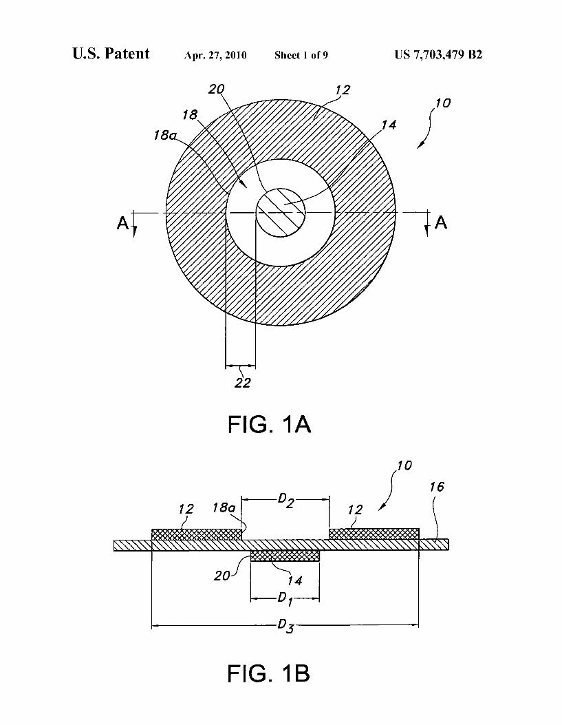
FIG. 1a is a top vieW of an actuator in accordance With one possible embodiment of the present invention disclosed herein;
FIG. 1b is a side cutaWay vieW taken along the line A-A of the actuator of FIG. 1a;
FIG. 2a is a perspective vieW of the actuator of FIG. 1a con?gured as a synthetic jet;
FIG. 2b is side cutaWay vieW taken along the line B-B of the actuator of FIG. 2a;
FIG. 3a is a perspective vieW of the actuator of FIG. 1a con?gured as a suction device;
FIG. 3b is a side cutaWay vieW taken along the line C-C of the actuator of FIG. 3a;
FIG. 4 is a representative schematic of a poWer circuit; FIGS. 5a, 6a, and 7a are photographs shoWing con?gura
tions of annular synthetic jets; FIGS. 5b, 6b, and 7b are representative side vieWs of the
actuators of FIGS. 5a, 6a, and 7a, respectively; FIGS. 8a-8d are top vieWs of various con?gurations of
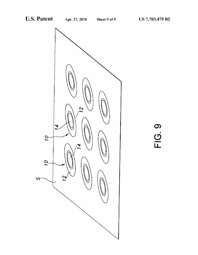
actuators; and FIG. 9 is a perspective vieW of a plurality of actuators
positioned on a surface.
DETAILED DESCRIPTION OF THE INVENTION
FIGS. 1 and 1a illustrate one possible embodiment of the inventive plasma actuator 10 of the present invention. When electrically activated, the actuator 10 produces a plasma that modi?es a ?uid ?oW in communication With the actuator 10. For example, it is envisioned that the actuator 10 may be used on an aerospace surface, such as an airfoil, for modifying the ?oW of air over the airfoil.
The actuator 10 includes ?rst and second conductors 12, 14 separated by a dielectric 16. Preferably, the conductors 12, 14 are positioned on opposite sides of the dielectric 16 (see FIG. 1a). This con?guration enables the actuator 10 to be installed substantially ?ush on a surface, as discussed beloW. As illus trated, the actuator 10 has an annular con?guration With the ?rst conductor 12 having the shape of a ring and the second conductor 14 having a substantially circular shape having a diameter D1. The center aperture 18 of the ring has a diameter D2 and de?nes an edge 18a. When D2 is greater than D1, a gap 22 is formed betWeen the edge 18a and an exterior edge 20 of the second conductor 14. In one embodiment, the diameter D2 is approximately 0.504", While the diameter D1 is approxi mately 0.5". This provides a gap 22 of approximately 0.4". Varying this gap 22 and the electrical poWer delivered to the actuator 10 enables a user to create various con?gurations of plasma synthetic jets or suction devices, as discussedbeloW in
20
25
30
35
40
45
50
55
60
65
4 further detail. Although the actuator 10 may be any siZe, in one embodiment, the outer diameter D3 of the conductor 12 is approximately 1". The conductors 12, 14 may be formed of any conductive or
semi-conductive material. In one embodiment, they are formed from copper tape having a thickness betWeen 0.001" 0.0l". The copper tape includes an adhesive backing that enables af?xation to the dielectric. Alternatively, the conduc tors 12, 14 may be etched directly onto the dielectric. For instance, copper coated surfaces may be surface etched using vapor deposition techniques, e.g., such as sputtering With a shadoW mask typically used in semi-conductor manufactur ing. In that case, the thickness of the conductors is betWeen 0.0000l"-0.05". Preferably, the conductors 12, 14 are a uni form thickness and each conductor has the same thickness. HoWever, the conductors 12, 14 could have a variable thick ness and/or each conductor 12, 14 may be con?gured With a different thickness.
The dielectric 16 may be formed of any material having minimal or substantially no electrical conductivity. For instance, it may be formed from KAPTON, TEFLON, alu mina ceramic, paper phenolic, acrylic, polycarbonate, or glass. Preferably, the dielectric Would have a thickness betWeen 0.001" and 0.25". Similar to the conductors 12, 14, the dielectric 16 preferably has a uniform thickness. HoW ever, the dielectric 16 could have a variable thickness.
To install the actuator 10, a user Will af?x the dielectric 16 bearing the ?rst and second conductors 12, 14 to a surface S in communication With a ?uid ?oW that the user desires to modify. In one embodiment, the surface S comprises an aero space surface, Wherein the ?uid ?oW Would be air, fuel, or a combination of air and fuel. The user may accomplish this by using an adhesive, a mechanical fastener, Welding, braZing, or otherWise. Once ?xed on the surface, the actuator Will have either the ?rst or second conductor 12, 14 exposed to the ambient ?uid F that the user desires to modify, With the other contacting the surface S. FIG. 2a illustrates the ?rst conductor 12 exposed to the ?uid F, While FIG. 3a illustrates the second conductor 14 exposed to the ?uid F. In some instances, it may be desirable to embed one of the conductors in the surface S, such as a distance H 1 from the surface S. One Will appreciate that unlike prior devices, the present actuator is substantially ?ush With the surface S When installed, such as the height H2 from the surface S (FIGS. 2b and 3b). At this point, one of the conductors 12, 14 becomes placed
in electrical communication With a poWer source, While the other becomes grounded. This presents another advantage of the present invention, namely, that a user may con?gure the actuator 10 for use as either a synthetic jet or as a suction device. To con?gure the actuator 10 as a synthetic jet, a user positions the ?rst conductor 12 in communication With the ?uid F, places the second conductor 14 in contact With the surface S, applies a voltage V1 to the ?rst conductor 12, and grounds the second conductor 14 (FIG. 2a). A skilled artisan Will appreciate that these steps may be completed in any order or simultaneously. Application of the voltage creates the plasma Pl, as represented in FIG. 2b. In this arrangement, ?uid F ?oWs aWay from the actuator in the direction Z 1 (FIG. 2b). Reversing this con?guration, such that the second con ductor 14 resides in communication With the ambient ?uid F, the ?rst conductor 12 contacts the surface S, and a user applies a voltage V1 to the second conductor 14, While grounding the ?rst conductor 12, results in the actuator acting as a suction device (FIG. 3a). Again, a skilled artisan Will appreciate that these steps may be completed in any order or simultaneously. Application of the voltage creates the plasma P1, as repre

US 7,703,479 B2 5
sented in FIG. 3b. In this con?guration, the ?uid F ?oWs toward the actuator in the direction Z2.
The conductors 12, 14 may receive electrical poWer in any knoWn manner. In one embodiment, an electrode 24 contacts one of the conductors 12, 14 and delivers electrical poWer from a poWer circuit 26 (FIGS. 2a, 3a). This electrode 24 may be formed from the same material as the conductors 12, 14, or any other material that enables it to deliver electrical poWer. FIG. 4 illustrates a representative poWer circuit 26 containing a poWer source 28, a transformer 30, and a function generator 32. In one embodiment, the poWer source 28 is a KEPCO 1-200V programmable poWer source and the transformer 30 is a 250 V primary/ 6 kV secondary step-up transformer. The function generator 32 may be integral With the poWer source 28 and provide a 3-5 kHZ sine, square, or triangular Wave input. The poWer circuit 26 may be a direct or alternating current circuit. Preferably, at least 1 kV Would be delivered to one of the conductors 12, 14, hoWever, any voltage and poWer circuit may be used, as long as it delivers enough voltage to create a plasma may be used.
Varying the voltage being delivered to one of the conduc tors 12, 14, as Well as the gap 22 betWeen the edges of the conductors 12, 14, results in various con?gurations of syn thetic jets or suction devices. For instance, applying a voltage betWeen 3 kV and 4 kV to an actuator having a gap 22 of 0.04" produces an annular jet having a plasma P WidthW1, as shoWn in FIGS. 5a and 5b. Increasing the voltage to betWeen 4 kV and 5 kV and providing a gap 22 of 0.04" produces an annular jet having a plasma Width W2, Which is greater than W 1 (FIGS. 6a and 6b). Further increasing the voltage to betWeen 5 kV and 6 kV creates a substantially disc shaped jet spanning betWeen the distance D2 across the center aperture 18 of the ?rst conductor 12 (FIGS. 7a and 7b). Accordingly, increasing the gap 22 increases the required voltage to achieve the same plasma Width.
In addition to being able to modify the geometry of the synthetic jet created, a user may create both continuous syn thetic jets and pulsed jets by ?uctuating or pulsing the poWer source to the actuator 10. This provides an enhanced level of user control for modifying a ?uid ?oW. Moreover, When con ?gured as a suction device, ?uctuating the poWer source to the actuator Will create continuous suction and pulsed suction, as desired. Unlike conventional ?oW controls that enable only a single mode of operation, the present actuator 10 provides a single device that may be operated in multiple modes.
Instead of the annular con?guration previously disclosed, the actuator 10 may have any other geometrical con?guration. For instance, the ?rst and second conductors 12, 14 may be any shape that de?nes an aperture 34, such as multiple ring shapes (FIG. 8a) or a star shape (FIG. 8b). Alternatively, the conductors 12, 14 may be substantially “v”-shaped, thereby forming a chevron having an angle (X betWeen 1° and 1790 When vieWed from the top (FIG. 80) or linear (FIG. 8d). One Will appreciate that one or more edges 18a of the ?rst con ductor 12 may de?ne a boundary 36, Wherein the second conductor 14 is positioned Within the boundary. For instance, the boundary 36 may be circular (FIG. 8a), star shape (FIG. 8b), “v”-shaped (FIG. 80), a plurality of straight lines (FIG. 8d), or otherwise. Also, as opposed to using a single actuator 10, a plurality of actuators 10 may be positioned on a surface S, as an array (FIG. 9). Each actuator 10 may be indepen dently controlled, thereby providing a user With further ?oW control. In any of these con?gurations, the actuator 10 and conductors 12, 14 may function as previously described.
20
25
30
35
40
45
50
55
60
65
6 Various experiments have been conducted or are proposed/
envisioned to demonstrate the above-described actuator. Details of one such actuator experiment are provided in the folloWing example.
EXAMPLE
Plasma actuators Were created using a conductive copper tape material. One actuator Was created in the form of an array of annular actuators, While the other Was created in a linear fashion. A 0.025" thick alumina ceramic slab Was used as the dielectric for a quiescent ?oW and ?at plate boundary layer experiment, While KAPTON Was used as the dielectric for a cylinder ?oW measurement. The diameters of exposed and embedded conductors of the
annular plasma synthetic jet actuator (“PSJA”) tested Were 1" and 0.5" respectively, With either no gap or a 0.04"-0.08" overlap. The dimensions of the linear synthetic jet actuator (“L-PSJA”) used in both quiescent ?oW and ?at plate experi ments Were chosen to match the PSJA, and the Width of the exposed conductors and embedded conductor of the L-PSJA Were 0.25" and 0.5" respectively, With no gap and a spanWise length of around 3.5". For quiescent ?oW measurements on the linear actuator, the Width of the exposed and embedded conductors Were about 6 mm, With spanWise lengths of around 3.5".
For the cylinder ?oW measurements, the exposed and embedded conductors for both L-PSJA and linear actuator Were 0.20" in Width (spanWise length of 20"), as the dimen sions of the cylinder used Was not large enough to accommo date the L-PSJA dimensions that matched the PSJA. The results for quiescent ?oW and ?at plate boundary layer experi ments Were obtained for a nominal 5 kV amplitude, 2.8 kHZ frequency square Wave AC input, operated With a 50% duty cycle. A nominal 2 kV amplitude, 1.1 kHZ frequency square Wave AC input operated With a 50% duty cycle Was used for the cylinder ?oW experiments.A function generator is used to provide a sinusoidal input to a KEPCO BPM-01 100 V poWer source. The output drives an non-inductively matched step-up transformer, Whose output is sent to the conductors. TWo step-up transformers Were used during the course of the experiments, one capable of 6 kV output With 1-250 V RMS input at 1-7 kHZ (Industrial Test Equipment Company, here inafter “T-l”) and the other capable of 5.5 kV output With 40 V RMS input at 6 kHZ (Corona Magnetics, Inc., hereinafter “T-2”). For measurements made With T-2, the exposed and embedded conductors Were driven With a 180° phase differ ence, While the embedded conductor Was grounded Whenever T-1 Was used. The input poWer Was monitored using a TEK TRONIX TDS channel oscilloscope, While a high voltage probe and current monitor Were used for voltage and current measurements, respectively, to determine input poWer.
The results of this experiment shoW that the plasma syn thetic jet actuator creates a ?oW structure very similar to that of a conventional synthetic jet, With a plasma induced jet being directed aWay from the surface, but Without the need of any moving parts. The jet is a Zero-mass ?ux since no addi tional ?uid is added to the system, but it does add momentum, and can thus be used to add momentum to a ?uid ?oW. The actuator can be turned on or off, or pulsed (such as, alternating on and off), so that input poWer to the actuator may be reduced. This also results in the actuator producing vortex rings instead of a steady jet Which also may be bene?cial. The present invention presents a ?uid actuator that can
modify a ?oW of ?uid Without the need for moving parts. The actuator alloWs for activation and deactivation, as desired. The actuator can also be mounted substantially ?ush With a

US 7,703,479 B2 7
surface, such that it may modify the ?oW Without signi?cantly projecting into it. The actuator can also operate as a synthetic jet for directing ?oW aWay from the actuator, as Well as a suction device for directing ?oW toWard the actuator. The foregoing discussion Was chosen to provide the best
illustration of the principles of the invention and its practical application to thereby enable one of ordinary skill in the art to utiliZe the invention in various embodiments and With various modi?cations suited to the particular use contemplated. For example, the gap 22 may be Zero or there may be overlap of the conductors 12, 14. Although the diameters D1, D2 Would preferably be no greater than 1", they may be any siZe. All modi?cations and variations are Within the scope of the inven tion as determined by the appended claims When interpreted in accordance With the breadth to Which they are fairly, legally and equitably entitled.
The invention claimed is: 1. A method of modifying a ?oW of ?uid, comprising: mounting a plurality of conductors on a surface, at least one
of said plurality of conductors de?ning an aperture; applying a voltage to at least one of the conductors,
Wherein the voltage creates a plasma; and creating a suction device With the plurality of conductors,
thereby resulting in a ?uid ?oW toWard the surface. 2. The method of claim 1, Wherein the mounting comprises
positioning the plurality of conductors substantially ?ush With the surface.
3. The method of claim 1, Wherein the applying a voltage comprises applying a substantially continuous voltage during the creating the suction device.
4. The method of claim 1, Wherein the applying a voltage comprises pulsing the voltage during the creating the suction device.
5. A method of modifying a ?oW of ?uid, comprising: mounting a plurality of conductors on a surface, at least one
of said plurality of conductors de?ning an aperture; applying a voltage to at least one of the conductors; and creating a plasma synthetic jet actuator With the plurality of
conductors, thereby resulting in a ?uid ?oW toWards or aWay from the surface.
6. The method of claim 5, Wherein the mounting comprises positioning the plurality of conductors substantially ?ush With the surface.
7. The method of claim 5, Wherein the applying a voltage comprises applying a substantially continuous voltage during the creating the synthetic jet actuator.
8. The method of claim 5, Wherein the applying a voltage comprises pulsing the voltage during the creating the syn thetic jet actuator.
9. A method of modifying a ?oW of ?uid, comprising: mounting a ?rst conductor on a ?rst side of a dielectric, the
?rst conductor having at least one edge that de?nes a boundary;
mounting a second conductor on a second side of a dielec tric, the second conductor is positioned Within the boundary;
applying a voltage to at least one of the conductors to modify a ?oW of ?uid in communication With one of the ?rst and second conductor.
20
25
30
35
40
45
50
55
8 10. A ?uid actuator, comprising: a ?rst and second conductor positioned on a dielectric,
Wherein one of the ?rst and second conductor de?nes an aperture and Whereby application of a voltage to the ?rst conductor creates a plasma betWeen the ?rst and second conductor, thereby modifying a ?oW of a ?uid in com munication With the actuator.
11. The ?uid actuator of claim 10, Wherein the application of the voltage to the ?rst conductor results in a ?uid ?oW aWay from the actuator.
12. The ?uid actuator of claim 10, Wherein the application of the voltage to the ?rst conductor results in a ?uid ?oW toWard the actuator.
13. The ?uid actuator of claim 10, Wherein the ?rst con ductor encircles the second conductor.
14. The ?uid actuator of claim 10, Wherein the ?rst con ductor is substantially ring shaped and the second conductor is circular.
15. The ?uid actuator of claim 14, further comprising a gap betWeen the ?rst conductor and the second conductor.
16. A system for modifying a ?uid ?oW, comprising: a surface; and an actuator including a ?rst and second conductor posi
tioned on a dielectric Wherein one of the ?rst and second conductor de?nes an aperture, and Whereby the actuator is connected to the surface and application of a voltage to the ?rst conductor creates a plasma betWeen the ?rst and second conductor, thereby directing a ?oW of a ?uid in communication With the actuator toWards or aWay from the surface.
17. The system of claim 16, Wherein the actuator is sub stantially ?ush With the surface.
18. The system of claim 16, Wherein the application of the voltage to the ?rst conductor results in a ?uid ?oW aWay from the actuator.
19. The system of claim 16, Wherein the application of the voltage to the ?rst conductor results in a ?uid ?oW toWard the actuator.
20. The system of claim 16, Wherein one of the ?rst and second conductor is embedded in the surface.
21. The system of claim 16, Wherein the surface includes a plurality of actuators, each independently controlled.
22. The system of claim 16, Wherein one of the ?rst and second conductor de?nes an aperture.
23. The system of claim 22, Wherein the ?rst conductor is substantially ring shaped and the second conductor is circular.
24. A ?uid actuator, comprising: a ?rst conductor positioned on a ?rst side of a dielectric, the
?rst conductor has at least one edge that de?nes a bound ary; and
a second conductor positioned on a second side of a dielec tric, Wherein the second conductor is positioned Within the boundary, and application of a voltage to one of the ?rst and second conductor creates a plasma, thereby modifying a ?oW of ?uid in communication With one of the ?rst and second conductor.
25. The ?uid actuator of claim 24, Wherein the ?rst and second conductor are substantially “v”-shaped.
* * * * *


![Plasma Virtual Actuators for Flow Controlfile.scirp.org/pdf/JFCMV_2015011516031995.pdf · 2015-01-15 · K.-S. Choi et al. 23 Figure 1. A typical configuration of DBD plasma actuator[4]](https://img.pdfslide.us/doc/110x75/5cb3ebbd88c99310568b80c0/plasma-virtual-actuators-for-flow-2015-01-15-k-s-choi-et-al-23-figure.jpg)