Embed Size (px)
Citation preview

Journal of Theoretical and Applied Information Technology 10
th October 2014. Vol. 68 No.1
© 2005 - 2014 JATIT & LLS. All rights reserved.
ISSN: 1992-8645 www.jatit.org E-ISSN: 1817-3195
27
VLSI DESIGN OF 12-BIT ADC WITH 1GSPS IN 180NM CMOS
INTEGRATING WITH SAR AND TWO-STEP FLASH ADC
1 K.LOKESH KRISHNA,
2 T.RAMASHRI
1Associate Professor, Department of ECE, Sri Venkateswara College of Engineering & Technology (Autonomous), Chittoor, Andhra Pradesh, India.
2 Professor, Department of ECE, Sri Venkateswara University College of Engineering, Tirupati, Andhra Pradesh, India.
E-mail: 1 [email protected] , 2 [email protected]
ABSTRACT
In this paper, a Novel Hybrid ADC consisting of two-step quantizer which has Flash ADC and SAR ADC along with Resistor String DAC is designed and implemented. This Hybrid ADC improves the speed by employing Flash ADC and resolution and power reduction can be achieved by utilizing SAR ADC. The Hybrid architecture carrying 12 bits as resolution, input frequency as 100MHz and sampling frequency is 1GHz. CMOS level schematic diagram of sub-blocks has been designed and implemented using Cadence Virtuoso 180nm technology at an operating voltage of 1.8 V. Layout design is captured using Virtuoso and then it is optimized for area. Based on the obtained result, INL and DNL has been identified as +0.034V to – 0.001V and + 0.06V to -0.05V respectively. The performance results show that the architecture achieves low power, high speed and less area.
Keywords: Sample and Hold Circuit, Comparator, Transmission Gate, Hybrid ADC, Two-step Quantizer,
SAR and Flash ADC.
1. INTRODUCTION
Modern wireless communications devices demand high data rates with low power consumption. One of the key components in the wireless receivers is the Analog to Digital Converter (ADC), which acts as interface between analog and digital domains. For System-on-Chip (SoC) applications, which often target portable applications require low voltage, low power and high resolution analog to digital converters. High-speed, medium – resolution and Low power are the important requirements in many wireless portable applications. Various ADC architectures such as Flash type, Folding, Subranging, Sigma-Delta and Pipeline have been used to deliver these requirements. Each architecture has its own advantages and disadvantages. But selection of an ADC depends upon the application and its specifications [1]-[8]. However no single ADC architecture can satisfy the requirements such as High-speed, medium – resolution and Low power. Hybrid Analog to Digital Converter (HADC) is a combination of different types of ADC’s for realizing different portions of the analog to digital converter to obtain better and improved design. The
hybrid designs are tremendously accepted approach for converter designs, because it has combined advantages of various converter techniques.
In this paper, a novel hybrid ADC circuit is implemented by using the two stages of ADC circuits based on pipelining method. Successive Approximation Register (SAR) ADC of 6-bits obtained from first stage and other 6-bits obtained from second stage with two step flash are combined to form 12-bit output. The two-step quantizer has one MSB (Most Significant Bits) ADC and one LSB (Least Significant Bits) ADC in which MSB ADC developed using 6-bit Successive Approximation Register ADC (SAR-ADC) logic and LSB ADC developed using 6-bit two-step Flash ADC. The output of this ADC is connected with thermometer decoder approach to avoid the glitches in the circuit. Hybrid ADC based on integrating ADC has been suitable for medium speed and medium resolution applications, but if the input bandwidth has been increased, the architecture cannot withstand and as number of bits increases, level of complexity also increases [9]. Also SAR and Dual-Slope based Hybrid ADC supports for

Journal of Theoretical and Applied Information Technology 10
th October 2014. Vol. 68 No.1
© 2005 - 2014 JATIT & LLS. All rights reserved.
ISSN: 1992-8645 www.jatit.org E-ISSN: 1817-3195
28
medium speed and medium resolution applications. But to implement this design with the help of main DAC and sub-DAC, requires more number of capacitor arrays even though it is separated. This may leads to high leakage in the ADC design [10]. A new hybrid architecture for ADC was proposed by [11] with robust high-resolution delta sigma modulator with single-bit output titled “Hybrid Delta-Sigma ADC”. This system consists of a low-order multi-bit analog noise-shaping loop, followed by a scaling block and a high-order single-bit digital modulator. The combination simplifies the realization of the analog modulator, and it allows the use of most of its full scale input range. The paper which discusses the two-step flash ADC for hybrid design has good advantage like low power consumption and it can be operated in high bandwidth, ultra high speed applications. This architecture has been proposed to implement an oversampled data converter [12]. To implement the hybrid SAR/Dual-slope ADC, change in duty cycle leads to affect sampling during short reset path of the cycle. To decide the linearity and resolution of SAR ADC capacitor array has been used in hybrid architecture. Even using this capacitor split, the Main DAC and sub DAC circuits which are need to implement MSB values still need capacitor ratio of 64 for both arrays. So it would be difficult to match the speed of the both ADC’s. In this paper design and development of an efficient Hybrid Analog to Digital Converter (ADC) in VLSI for high frequency RF applications is discussed.
Section II introduces ADC, section III discusses hybrid ADC with design specification, section IV discusses design of proposed hybrid ADC, section V discusses results and section VI is conclusion.
2. ANALOG TO DIGITAL CONVERTER:
Data converters are recognized as converting one form of signal into another form of signal. The data converters are of two types (i) Analog to digital converter (ADC) (ii) Digital to analog converter (DAC). The Figure 1, shows the block diagram of analog to digital converter which has analog signal as input and gives binary output.
Hybrid Analog to Digital Converter (HADC) is a combination of different types of ADC’s for realizing different portions of the analog to digital converter to obtain better design. In this paper, we propose a novel hybrid circuit by using the two-step quantizer. This paper carries 12-bits where 6-bits obtained from first stage and other 6-bits obtained from second stage. The first stage has SAR ADC to generate MSB (Most Significant Bits), and LSBs (Least Significant Bits) have been generated by Flash ADC. This two-step quantizer has been designed using flash ADC, which consists of a resistor divider network that generates a “Ladder” of reference voltages, and comparators that compare the input to the reference voltages. Decoding logic is used to take the comparator decisions and generate a digital output code. A flash converter needs 2N resistors and 2N-1 comparators for an N-bit output code. The flash ADC is faster but has the limitation due to the exponential growth of comparators and resistors with respect to number of bits. For this reason, flash converters are generally used in applications requiring high speed and low resolution (<8bits). The LSBs has been designed using Flash ADC logic. Another architecture chosen to implement the HADC is Successive Approximation Register (SAR) ADC, which is good for supporting low to medium speeds. Its architecture is widely used to implement the low power design. The SAR ADC is designed to generate the Most Significant Bits of two-step quantizer. The working of SAR ADC is based on the binary search algorithm with respect to the input signal. This logic can be implemented using N-bit shift registers, where the input signal will be converted with respect to reference voltage. This voltage will be compared with input signal and provides the digital output by shifting or holding the value stored in the shift register. The HADC consists of Flash architecture to improve the speed of the design, and SAR ADC has been employed to enhance the resolution of the device.
3. HYBRID ADC ARCHITECTURE DESIGN:
The design specifications for Hybrid ADC are shown in Table 1.
Figure1: Basic ADC Architecture [13]

Journal of Theoretical and Applied Information Technology 10
th October 2014. Vol. 68 No.1
© 2005 - 2014 JATIT & LLS. All rights reserved.
ISSN: 1992-8645 www.jatit.org E-ISSN: 1817-3195
29
The proposed block diagram of Hybrid ADC is shown in Figure 2. It consists of two stages, in which first stage has been developed using 6-bit SAR ADC and second stage has been developed by
using 6-bit two-step Flash ADC. It consists of S/H circuit, subtractor with gain stage, DAC, Flash ADC and SAR ADC.
4. DESIGN OF SUBSYSTEMS:
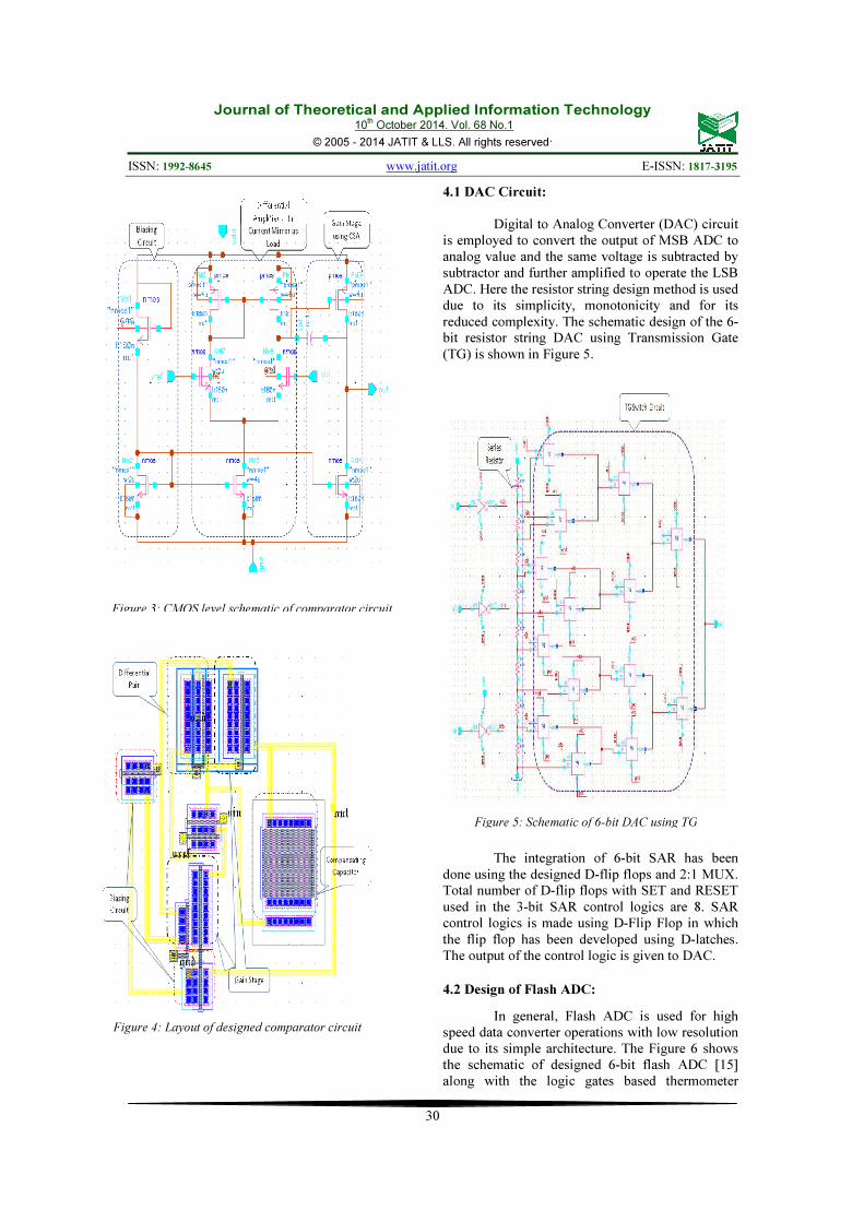
Comparator is an important circuit in analog and mixed signal designs. The HADC consists of Flash and SAR architecture, in which comparator is used as important block to compute the decision. The two stage operational amplifier is used as a comparator. The Figure 3 shows the designed schematic of comparator circuit [14] and Figure 4 shows the layout implementation of designed comparator. The first stage of the designed comparator consists of two parts, one is biasing circuit to bias the current mirror and another part is differential amplifier (DA). The second stage is gain stage to improve the gain of operational amplifier.
Table1:Hybrid ADC Design Specifications
Parameter Hybrid ADC
Resolution 12-bits
Input Voltage 1.8 V
Reference Voltage 1.8 V
Technology 180nm CMOS
Input Bandwidth 100 MHz
Sampling Frequency 1 GHz
Power Dissipation 1 mW
SNR 74 dB
INL / DNL ± 0.3 LSB
Figure2: Top level block diagram of Hybrid ADC
Journal of Theoretical and Applied Information Technology 10
th October 2014. Vol. 68 No.1
© 2005 - 2014 JATIT & LLS. All rights reserved.
ISSN: 1992-8645 www.jatit.org E-ISSN: 1817-3195
30
4.1 DAC Circuit:
Digital to Analog Converter (DAC) circuit is employed to convert the output of MSB ADC to analog value and the same voltage is subtracted by subtractor and further amplified to operate the LSB ADC. Here the resistor string design method is used due to its simplicity, monotonicity and for its reduced complexity. The schematic design of the 6-bit resistor string DAC using Transmission Gate (TG) is shown in Figure 5.
The integration of 6-bit SAR has been done using the designed D-flip flops and 2:1 MUX. Total number of D-flip flops with SET and RESET used in the 3-bit SAR control logics are 8. SAR control logics is made using D-Flip Flop in which the flip flop has been developed using D-latches. The output of the control logic is given to DAC.
4.2 Design of Flash ADC:
In general, Flash ADC is used for high speed data converter operations with low resolution due to its simple architecture. The Figure 6 shows the schematic of designed 6-bit flash ADC [15] along with the logic gates based thermometer
Figure 3: CMOS level schematic of comparator circuit
Figure 4: Layout of designed comparator circuit
Figure 5: Schematic of 6-bit DAC using TG

Journal of Theoretical and Applied Information Technology 10
th October 2014. Vol. 68 No.1
© 2005 - 2014 JATIT & LLS. All rights reserved.
ISSN: 1992-8645 www.jatit.org E-ISSN: 1817-3195
31
decoder to convert the thermometer code into binary code. In Flash ADC architecture, the reference voltage is divided by the resistive divider network, which gives different node voltages. The divided node voltage is compared with analog sampled input voltage by comparator. The output of the comparator produces the thermometric codes and these generated thermometric codes is converted to binary form using logic gates based thermometer decoder.
circuit design has been designed as per the specifications identified in Table 1. “Nplusres” from the GPDK 180nm library with the resistance of 22 Ω has been used as a resistor in voltage divider circuit. The resistor has been divided into 5 segments to reduce the area, power consumption and improve the speed. 4.3 Integration of Flash ADC and SAR ADC:
The Figure 7 shows the designed 6-bit two-step flash ADC circuit and Figure 8 shows the designed 6-bit SAR ADC.
Figure 6: Schematic of 6-bit Flash ADC with Thermometer code to binary code converter
Figure 7: Two-Step 6-bit Flash ADC
Figure 8: 6-Bit SAR ADC Schematic
Journal of Theoretical and Applied Information Technology 10
th October 2014. Vol. 68 No.1
© 2005 - 2014 JATIT & LLS. All rights reserved.
ISSN: 1992-8645 www.jatit.org E-ISSN: 1817-3195
32
5. RESULTS AND DISCUSSIONS:
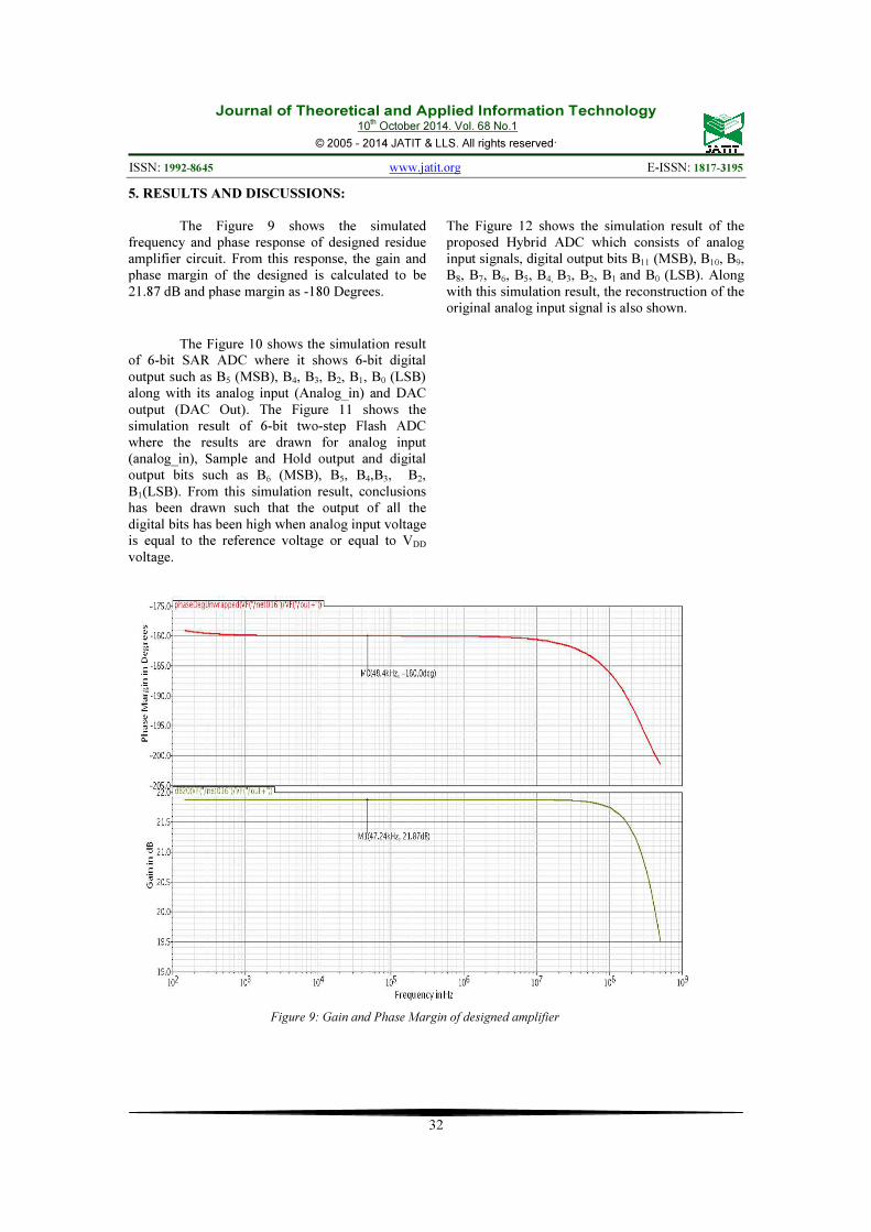
The Figure 9 shows the simulated frequency and phase response of designed residue amplifier circuit. From this response, the gain and phase margin of the designed is calculated to be 21.87 dB and phase margin as -180 Degrees.
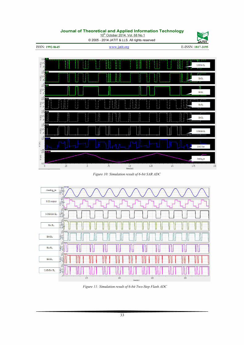
The Figure 10 shows the simulation result of 6-bit SAR ADC where it shows 6-bit digital output such as B5 (MSB), B4, B3, B2, B1, B0 (LSB) along with its analog input (Analog_in) and DAC output (DAC Out). The Figure 11 shows the simulation result of 6-bit two-step Flash ADC where the results are drawn for analog input (analog_in), Sample and Hold output and digital output bits such as B6 (MSB), B5, B4,B3, B2, B1(LSB). From this simulation result, conclusions has been drawn such that the output of all the digital bits has been high when analog input voltage is equal to the reference voltage or equal to VDD voltage.
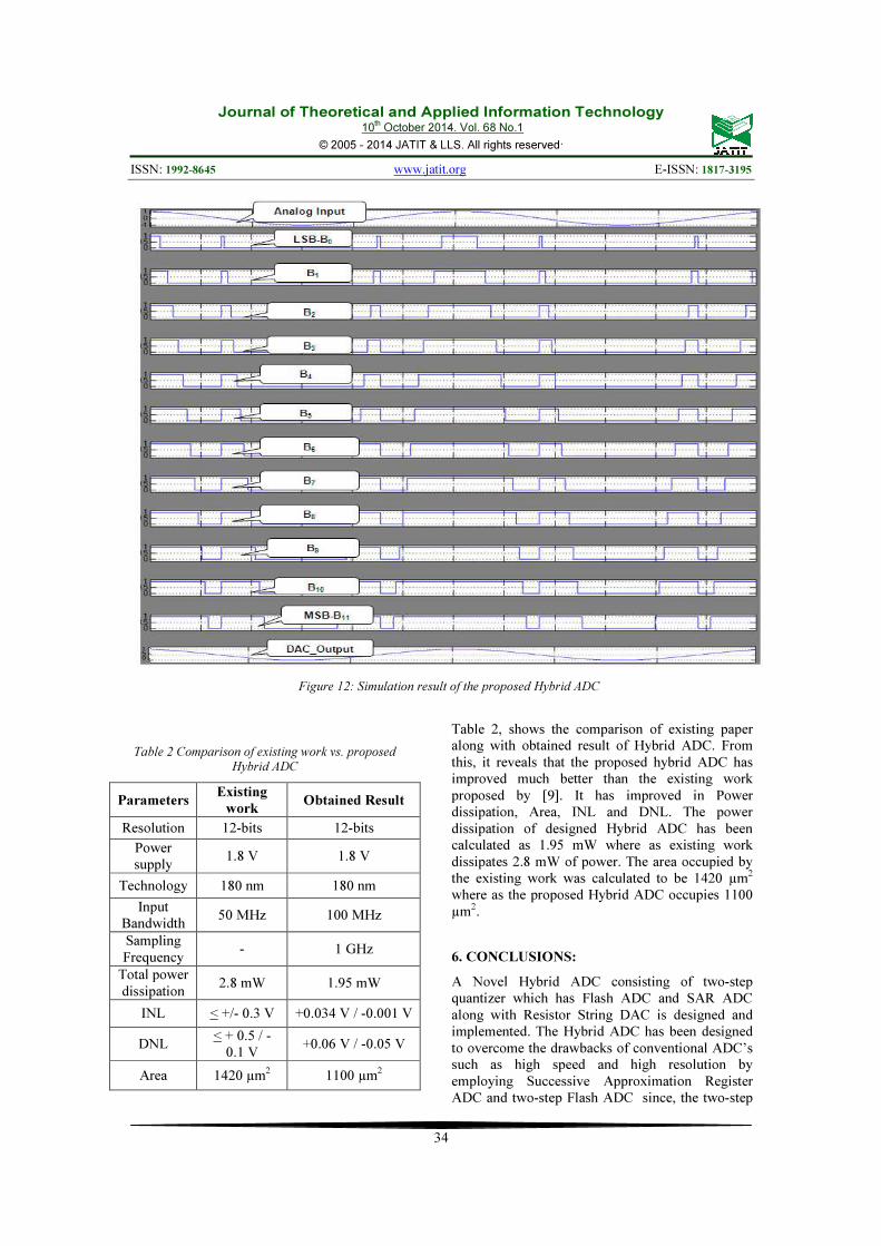
The Figure 12 shows the simulation result of the proposed Hybrid ADC which consists of analog input signals, digital output bits B11 (MSB), B10, B9, B8, B7, B6, B5, B4, B3, B2, B1 and B0 (LSB). Along with this simulation result, the reconstruction of the original analog input signal is also shown.
Figure 9: Gain and Phase Margin of designed amplifier
Journal of Theoretical and Applied Information Technology 10
th October 2014. Vol. 68 No.1
© 2005 - 2014 JATIT & LLS. All rights reserved.
ISSN: 1992-8645 www.jatit.org E-ISSN: 1817-3195
33
Figure 11: Simulation result of 6-bit Two-Step Flash ADC
Figure 10: Simulation result of 6-bit SAR ADC
Journal of Theoretical and Applied Information Technology 10
th October 2014. Vol. 68 No.1
© 2005 - 2014 JATIT & LLS. All rights reserved.
ISSN: 1992-8645 www.jatit.org E-ISSN: 1817-3195
34
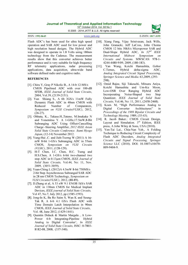
Table 2, shows the comparison of existing paper along with obtained result of Hybrid ADC. From this, it reveals that the proposed hybrid ADC has improved much better than the existing work proposed by [9]. It has improved in Power dissipation, Area, INL and DNL. The power dissipation of designed Hybrid ADC has been calculated as 1.95 mW where as existing work dissipates 2.8 mW of power. The area occupied by the existing work was calculated to be 1420 µm2
where as the proposed Hybrid ADC occupies 1100 µm2.
6. CONCLUSIONS:
A Novel Hybrid ADC consisting of two-step quantizer which has Flash ADC and SAR ADC along with Resistor String DAC is designed and implemented. The Hybrid ADC has been designed to overcome the drawbacks of conventional ADC’s such as high speed and high resolution by employing Successive Approximation Register ADC and two-step Flash ADC since, the two-step
Table 2 Comparison of existing work vs. proposed Hybrid ADC
Parameters Existing
work Obtained Result
Resolution 12-bits 12-bits
Power supply
1.8 V 1.8 V
Technology 180 nm 180 nm
Input Bandwidth
50 MHz 100 MHz
Sampling Frequency
- 1 GHz
Total power dissipation
2.8 mW 1.95 mW
INL < +/- 0.3 V +0.034 V / -0.001 V
DNL < + 0.5 / -
0.1 V +0.06 V / -0.05 V
Area 1420 µm2 1100 µm2
Figure 12: Simulation result of the proposed Hybrid ADC
Journal of Theoretical and Applied Information Technology 10
th October 2014. Vol. 68 No.1
© 2005 - 2014 JATIT & LLS. All rights reserved.
ISSN: 1992-8645 www.jatit.org E-ISSN: 1817-3195
35
Flash ADC’s has been used for ultra high speed operation and SAR ADC used for low power and high resolution based designs. The Hybrid ADC was designed to operate in 1.8 Volts using 180nm technology from the Cadence. The measurement results show that this converter achieves better performance and is very suitable for high frequency RF telemetry applications, radar processing applications, data acquisition, ultra-wide band software defined radio and cognitive radio.
REFERENCES
[1]. Chiru Y, Gray P Nikolic B., A 14-b 12-MS/s CMOS Pipelined ADC with over 100-dB
SFDR, IEEE Journal of Solid State Circuits, 2004, Vol.39, (2139-2151).
[2]. Yun Shiang S., A 6b 3GS/s 11mW Fully Dynamic Flash ADC in 40nm CMOS with Reduced Number of Comparators, Symposium on VLSI Ciruits(VLSIC), 2012, (26-27).
[3]. Ohhata, K., Takase.H.,Tateno, M.Imakake N and Yonemitsu Y. A 1-GHz,17.5mW,8-Bit Subranging ADC Using Offset-Cancelling Charge -Steering Amplifier, 2012 IEEE Asian
Solid State Circuits Conference. Itami Hyogo
Japan, (12-14) November 2012. [4]. Yung-Hui ,C. and Jieh-Tsorng W (2011) A 16-
mW 8-bit 1-GS/s Subranging ADC in 55nm CMOS, Symposium on VLSI Circuits
(VLSIC), 2011, (128-129). [5]. H-T Chen, I.C. Chen, H.C. Tseng and
H.S.Chen, A 1-GS/s 6-bit two-channel two step ADC in 0.13µm CMOS, IEEE Journal of
Solid State Circuits, Vol.44, No: 11, Nov. 2009, (3051-3059).
[6]. Yuan-Ching L (2012)A 4.5mW 8-bit 750MS/s 2-bit Step Asynchronous Subranged SAR ADC in 28 nm CMOS Technology, Symposium on
VLSI Circuits(VLSIC), 2012, (88-89). [7]. D.Zhang et al, A 53 nW 9.1 ENOB 1kS/s SAR
ADC in 130nm CMOS for Medical Implant Devices, IEEE journal of Solid State Circuits,
Vol 47, No.7, July 2012, pp (1585-1593). [8]. Jong-In K, Ba Ro Saim S, Wan K and Seung-
Tak R, A 6-b 4.1 GS/s Flash ADC with Time Domain Latch Interpolation in 90nm CMOS, IEEE Journal of Solid State Circuits,
Vol. 48, June 2012, (1429-1441). [9]. Quentin Diduck & Martin Margala , A Low-
Power 6-b Integrating-Pipeline Hybrid Analog to Digital Converter’, In IEEE
Journal of Solid State Circuits, ISSC: 0-7803-8182-08, 2008, (337-340).
[10]. Xiang Fang, Vijay Srinivasan, Jack Wills, John Granacki, Jeff LaCoss, John Choma CMOS 12 bits 50kS/s Micropower SAR and Dual-Slope Hybrid ADC, In 52
nd IEEE
International Midwest Symposium on
Circuits and Systems. MWSCAS: 978-1- 4244-4480-9/09, 2009, (180-183).
[11]. Yan Wang, Koichi Hamashita, Gobor C.Temes, Hybrid delta-sigma ADC, Analog Integrated Circuit Signal Processing,
Springer Science and Media. 63,2009, (293- 298). [12]. Omid Rajee, Siji Takeuchi, Mitsuru Aniya,
Koichi Hamashita and Um-Ku Moon, Low-OSR Over Ranging Hybrid ADC Incorporating Noise-Shaped two Step Quantizer, IEEE Journal of Solid State
Circuits, Vol.46, No: 11, 2011, (2458-2468). [13]. Koen. M, “High Performance Analog to
Digital Converter Architectures” in
Proceedings of the 1989 Bipolar Circuits and
Technology Meeting, 1989, (35-43). [14]. R. Jacob Baker.: CMOS Circuit Design,
Layout and Simulation. 3rd Edition, IEEE press, A John Wiley & Sons, USA (2010).
[15]. Yen-Tai Lai., Chia-Nan Yeh., A Folding Technique to Reducing Circuit Complexity of
Flash ADC Decoders, Analog Integrated
Circuits and Signal Processing, Springer
Science LLC (2010). DOI: 10.1007/s10470- 009-9404-9.