Embed Size (px)
Citation preview
1 Introduction
1.1 Organic Molecular ElectronicsIn the application of organic molecules to
electronics, passive materials such as insulat-ing materials have been the main streams inthe study. These materials have been veryimportant in the electronics but did not consti-tute the main stream in the characteristics ofdevices. Also, in the technique and the mate-rials of the so-called “solid-state electronics”,which support current information system,organic molecules have been used in electron-ic parts, electronic insulating materials andcoating materials as the materials of deviceswith special features in insulating and dielec-tric functions.
Under such circumstances, several decadeshave elapsed already since organic molecularelectronics have been proposed and havebecome the object of the study with a basicconcept to apply organic molecules in active
electric materials (e.g. rectifying device, tran-sistor device, etc.) by using organic moleculesas materials. The organic molecular electronicdevice as initially proposed was a device toprovide electronic functions (such as rectify-ing function and transistor function) in a syn-thesized single molecule [1]. With such con-cept, it was tried to break through the limits ofconventional Si device. At that time, it wouldhave been impossible to actually prepare adevice consisting of a single molecule and toverify its function. This was because therewere technical problems in synthesizing a rel-atively large molecule, which has an electron-ic functional group in a molecule, from theviewpoint of molecular synthesis. Also, it wasbecause there were problems of electronicaccess or contact to a single molecule in ultra-fine size of nano or sub-nano scale from exter-nal environment such as electronic measuringinstruments and devices. For this reason, thestudy of organic electronics in earlier stage
KUBOTA Tohru et al. 99
4-2 Single Molecular Electronics
KUBOTA Tohru, NAGASE Takashi, HASEGAWA Hiroyuki, and MASHIKO Shinro
In recent years, nano-technology may lead to a new way to electronics and many novelelectronic devices in the field of information and communications technology. One of thesenano-devices, single electron tunneling device using small particles in their systems havebeen successfully prepared, high-density memory devices, high-speed low power switchingdevices, high-sensitive electrometer devices and others will be produced in near future.However these are not sufficient. Using an organic molecule as a coulomb island electrode,it is possible to use a potential ability of the molecules. In the present paper, we fabricatethe some types of organic SET device, using organic and inorganic insulator, and ultra-nar-row nano-gap electrodes, and investigate the electrical properties of these single electrontunneling devices with or without light irradiation. We are making effort to adding specificoptical and electronic properties coming from individual organic molecules to our singleelectron tunneling devices.
Keywords Molecular electronics, Single electron tunneling device, Organic molecule, Light gatedevice, Nano-gap electrodes
100
has been mostly concentrated on the studybased on molecular aggregate, which is rela-tively easy to produce. From the studies onvarious types of materials, devices and inter-face, a number of organic devices for practicaluse such as liquid crystal, EL device, etc.have been prepared. In recent years, a widevariety of features such as flexibility, light-weight property, economic feasibility, diversi-ty, etc., which are characteristic of functionsof organic materials, have been added to thesepractical devices and studies have beenadvancing. As a result, these features are nowimportant factors in the manufacture of futureorganic devices. The studies are now flourish-ing, and it is attempted to produce the devicesby achieving the functions of molecular crys-tals, molecular thin-film and macromolecularthin-film in the regions of ultra-fine size andon nano level. Emphasis is put on flexibility,e.g. in the development of organic FET, forwhich studies are made to achieve practicaluse. It is generally said that the control ofphysical properties on nano level and molecu-lar level is important for the improvement ofperformance characteristics.
1.2 Single Molecular ElectronicsThe techniques to prepare organic molecu-
lar film in ultra-fine size (top-down) or toorganize organic molecules (bottom-up) andthe development of tools to directly evaluateand to have access to molecules such as STM,AFM, etc. has been advancing. Now, thebasis to create “single molecular device” toprovide active electronic function to a singlemolecule, as initially proposed for organicmolecular electronics, has been consolidatedto full extent although it is still in the stage ofresearch. In fact, several studies [2]-[4] for theevaluation of electrical properties of singlemolecule have appeared. In future, it shouldbe tried to apply the results of these studies forthe research to prepare single moleculardevice, which represents the true aspect of theinitial organic molecular electronics, withoutterminating these studies in mere stage oftechnique and evaluation. In this technical
field, not only more researchers should beengaged in the evaluation of physical proper-ties of organic molecules, but also they shouldhave more clearly defined image of the deviceand should continue to study with more chal-lenging spirit.
Then, for the purpose of creating singlemolecular electronics and electronic systembased on it, which type of active electronicfunctions should we seek in the single mole-cule? As one of the replies to such question,our study group is aiming to achieve organicelectronic device of the next generation ininformation and communication field. We aretrying to take advantage of the characteristicsof single organic material and are seeking thefeatures, which the conventional Si type inor-ganic material could not attain, and we arealso trying to develop single electron tunnel-ing (SET) device using the organic molecule.The SET device itself has a structure withsmall particles formed in electrical tunnelingbarrier as Coulomb Island, and various appli-cations have been conceived including memo-ry device, high-speed low-power switchingdevice, high-sensitive electrometer device, etc.[5] [6]. With the progress of ultra-fine litho-graphic technique to produce semiconductordevices, the development of new devices isnow in progress based on quantum effect, andthis is one of the important research fields forinorganic semiconductor materials. In addi-tion to such features, based on the use oforganic molecule, it is now possible to add thefeatures of organic molecule such as ultra-fineproperty, photo-responsibility, self-organizingability, flexibility, etc. This makes it possibleto attain new functions while taking advantageof the conventional type SET device. In thepresent report, we take special notice on ultra-fine property and photo-responsibility oforganic molecule and introduce the results ofthe study to the device using single organicmolecule as Coulomb Island for SET device.Further, we will discuss the possibility ofattaining organic SET device.
Journal of the National Institute of Information and Communications Technology Vol.51 Nos.3/4 2004
2 Development of Single ElectronTunneling Device using OrganicMolecule as Coulomb Island [7]-[10]
As already described, the study is nowbeing made on molecular electronics withaims to provide electronic functions and opti-cal functions of a single molecule by usingorganic molecule and to apply the functions toelectronic-optical device. Above all, attentionis focused on the functions of single molecule,and the study of single electron tunneling(SET) device in the single molecular electron-ics for application of electronic device is nowone of the important research fields togetherwith the study on the development to systemintegration and on the application of varioustypes of devices.
2.1 Single Electron Tunneling DeviceSingle electron tunneling device is defined
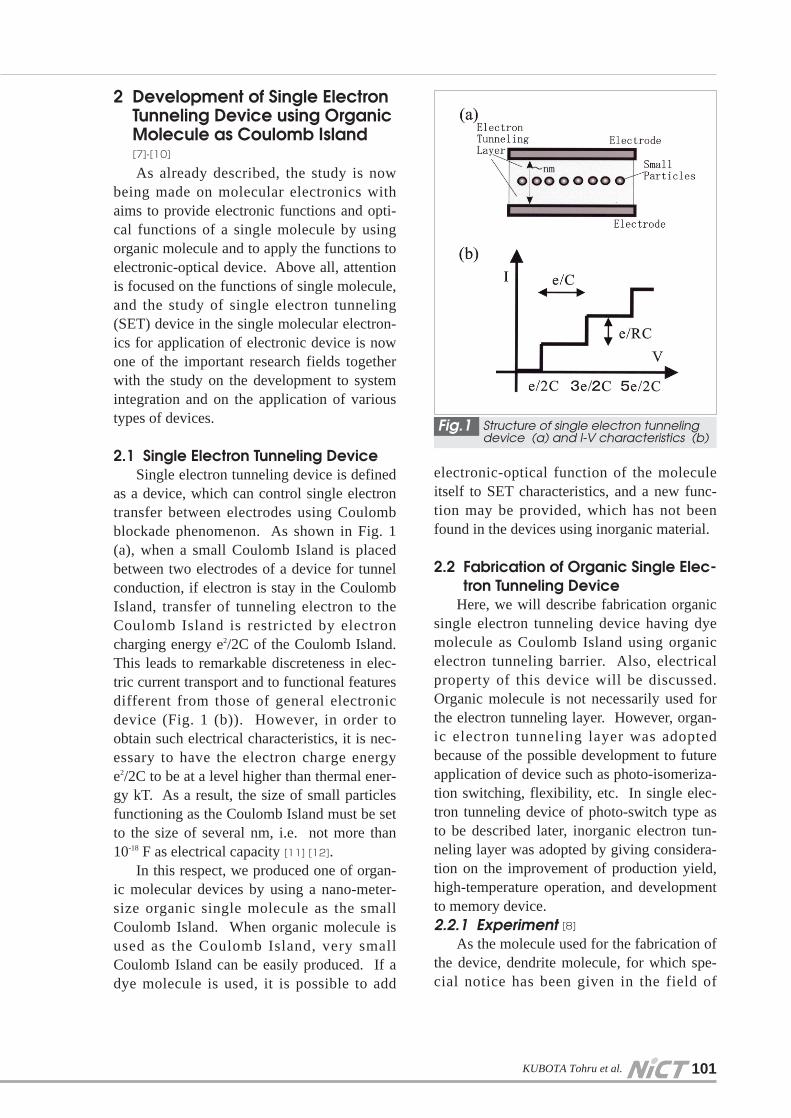
as a device, which can control single electrontransfer between electrodes using Coulombblockade phenomenon. As shown in Fig. 1(a), when a small Coulomb Island is placedbetween two electrodes of a device for tunnelconduction, if electron is stay in the CoulombIsland, transfer of tunneling electron to theCoulomb Island is restricted by electroncharging energy e2/2C of the Coulomb Island.This leads to remarkable discreteness in elec-tric current transport and to functional featuresdifferent from those of general electronicdevice (Fig. 1 (b)). However, in order toobtain such electrical characteristics, it is nec-essary to have the electron charge energye2/2C to be at a level higher than thermal ener-gy kT. As a result, the size of small particlesfunctioning as the Coulomb Island must be setto the size of several nm, i.e. not more than10-18 F as electrical capacity [11] [12].
In this respect, we produced one of organ-ic molecular devices by using a nano-meter-size organic single molecule as the smallCoulomb Island. When organic molecule isused as the Coulomb Island, very smallCoulomb Island can be easily produced. If adye molecule is used, it is possible to add
electronic-optical function of the moleculeitself to SET characteristics, and a new func-tion may be provided, which has not beenfound in the devices using inorganic material.
2.2 Fabrication of Organic Single Elec-tron Tunneling Device
Here, we will describe fabrication organicsingle electron tunneling device having dyemolecule as Coulomb Island using organicelectron tunneling barrier. Also, electricalproperty of this device will be discussed.Organic molecule is not necessarily used forthe electron tunneling layer. However, organ-ic electron tunneling layer was adoptedbecause of the possible development to futureapplication of device such as photo-isomeriza-tion switching, flexibility, etc. In single elec-tron tunneling device of photo-switch type asto be described later, inorganic electron tun-neling layer was adopted by giving considera-tion on the improvement of production yield,high-temperature operation, and developmentto memory device.2.2.1 Experiment [8]
As the molecule used for the fabrication ofthe device, dendrite molecule, for which spe-cial notice has been given in the field of
KUBOTA Tohru et al. 101
Structure of single electron tunnelingdevice (a) and I-V characteristics (b)
Fig.1
102
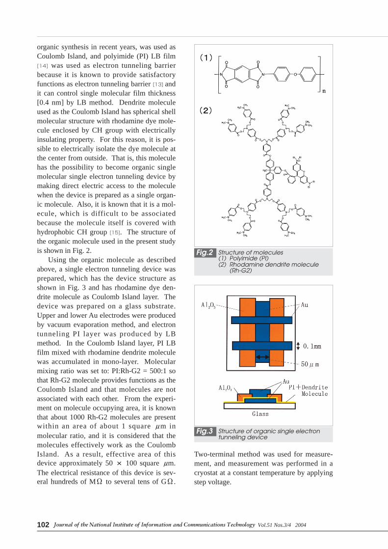
organic synthesis in recent years, was used asCoulomb Island, and polyimide (PI) LB film[14] was used as electron tunneling barrierbecause it is known to provide satisfactoryfunctions as electron tunneling barrier [13] andit can control single molecular film thickness[0.4 nm] by LB method. Dendrite moleculeused as the Coulomb Island has spherical shellmolecular structure with rhodamine dye mole-cule enclosed by CH group with electricallyinsulating property. For this reason, it is pos-sible to electrically isolate the dye molecule atthe center from outside. That is, this moleculehas the possibility to become organic singlemolecular single electron tunneling device bymaking direct electric access to the moleculewhen the device is prepared as a single organ-ic molecule. Also, it is known that it is a mol-ecule, which is difficult to be associatedbecause the molecule itself is covered withhydrophobic CH group [15]. The structure ofthe organic molecule used in the present studyis shown in Fig. 2.
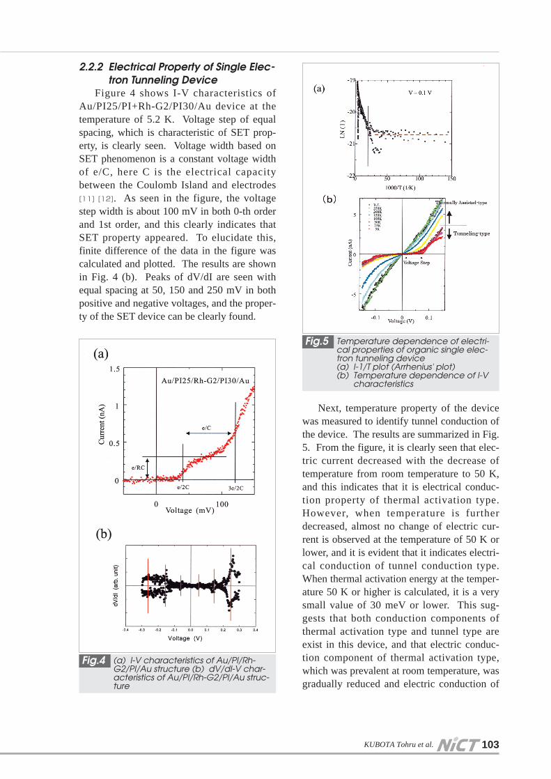
Using the organic molecule as describedabove, a single electron tunneling device wasprepared, which has the device structure asshown in Fig. 3 and has rhodamine dye den-drite molecule as Coulomb Island layer. Thedevice was prepared on a glass substrate.Upper and lower Au electrodes were producedby vacuum evaporation method, and electrontunneling PI layer was produced by LBmethod. In the Coulomb Island layer, PI LBfilm mixed with rhodamine dendrite moleculewas accumulated in mono-layer. Molecularmixing ratio was set to: PI:Rh-G2 = 500:1 sothat Rh-G2 molecule provides functions as theCoulomb Island and that molecules are notassociated with each other. From the experi-ment on molecule occupying area, it is knownthat about 1000 Rh-G2 molecules are presentwithin an area of about 1 square μm inmolecular ratio, and it is considered that themolecules effectively work as the CoulombIsland. As a result, effective area of thisdevice approximately 50 × 100 square μm.The electrical resistance of this device is sev-eral hundreds of MΩ to several tens of GΩ.
Two-terminal method was used for measure-ment, and measurement was performed in acryostat at a constant temperature by applyingstep voltage.
Journal of the National Institute of Information and Communications Technology Vol.51 Nos.3/4 2004
Structure of molecules(1) Polyimide (PI)(2) Rhodamine dendrite molecule
(Rh-G2)
Fig.2
Structure of organic single electrontunneling device
Fig.3
2.2.2 Electrical Property of Single Elec-tron Tunneling Device
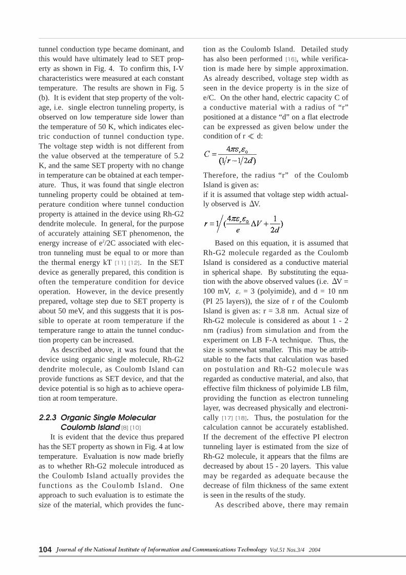
Figure 4 shows I-V characteristics ofAu/PI25/PI+Rh-G2/PI30/Au device at thetemperature of 5.2 K. Voltage step of equalspacing, which is characteristic of SET prop-erty, is clearly seen. Voltage width based onSET phenomenon is a constant voltage widthof e/C, here C is the electrical capacitybetween the Coulomb Island and electrodes[11] [12]. As seen in the figure, the voltagestep width is about 100 mV in both 0-th orderand 1st order, and this clearly indicates thatSET property appeared. To elucidate this,finite difference of the data in the figure wascalculated and plotted. The results are shownin Fig. 4 (b). Peaks of dV/dI are seen withequal spacing at 50, 150 and 250 mV in bothpositive and negative voltages, and the proper-ty of the SET device can be clearly found.
Next, temperature property of the devicewas measured to identify tunnel conduction ofthe device. The results are summarized in Fig.5. From the figure, it is clearly seen that elec-tric current decreased with the decrease oftemperature from room temperature to 50 K,and this indicates that it is electrical conduc-tion property of thermal activation type.However, when temperature is furtherdecreased, almost no change of electric cur-rent is observed at the temperature of 50 K orlower, and it is evident that it indicates electri-cal conduction of tunnel conduction type.When thermal activation energy at the temper-ature 50 K or higher is calculated, it is a verysmall value of 30 meV or lower. This sug-gests that both conduction components ofthermal activation type and tunnel type areexist in this device, and that electric conduc-tion component of thermal activation type,which was prevalent at room temperature, wasgradually reduced and electric conduction of
KUBOTA Tohru et al. 103
(a) I-V characteristics of Au/PI/Rh-G2/PI/Au structure (b) dV/dI-V char-acteristics of Au/PI/Rh-G2/PI/Au struc-ture
Fig.4
Temperature dependence of electri-cal properties of organic single elec-tron tunneling device(a) I-1/T plot (Arrhenius' plot)(b) Temperature dependence of I-V
characteristics
Fig.5
104
tunnel conduction type became dominant, andthis would have ultimately lead to SET prop-erty as shown in Fig. 4. To confirm this, I-Vcharacteristics were measured at each constanttemperature. The results are shown in Fig. 5(b). It is evident that step property of the volt-age, i.e. single electron tunneling property, isobserved on low temperature side lower thanthe temperature of 50 K, which indicates elec-tric conduction of tunnel conduction type.The voltage step width is not different fromthe value observed at the temperature of 5.2K, and the same SET property with no changein temperature can be obtained at each temper-ature. Thus, it was found that single electrontunneling property could be obtained at tem-perature condition where tunnel conductionproperty is attained in the device using Rh-G2dendrite molecule. In general, for the purposeof accurately attaining SET phenomenon, theenergy increase of e2/2C associated with elec-tron tunneling must be equal to or more thanthe thermal energy kT [11] [12]. In the SETdevice as generally prepared, this condition isoften the temperature condition for deviceoperation. However, in the device presentlyprepared, voltage step due to SET property isabout 50 meV, and this suggests that it is pos-sible to operate at room temperature if thetemperature range to attain the tunnel conduc-tion property can be increased.
As described above, it was found that thedevice using organic single molecule, Rh-G2dendrite molecule, as Coulomb Island canprovide functions as SET device, and that thedevice potential is so high as to achieve opera-tion at room temperature.
2.2.3 Organic Single MolecularCoulomb Island [8] [10]
It is evident that the device thus preparedhas the SET property as shown in Fig. 4 at lowtemperature. Evaluation is now made brieflyas to whether Rh-G2 molecule introduced asthe Coulomb Island actually provides thefunctions as the Coulomb Island. Oneapproach to such evaluation is to estimate thesize of the material, which provides the func-
tion as the Coulomb Island. Detailed studyhas also been performed [16], while verifica-tion is made here by simple approximation.As already described, voltage step width asseen in the device property is in the size ofe/C. On the other hand, electric capacity C ofa conductive material with a radius of “r”positioned at a distance “d” on a flat electrodecan be expressed as given below under thecondition of r ≪ d:
Therefore, the radius “r” of the CoulombIsland is given as:if it is assumed that voltage step width actual-ly observed is ΔV.
Based on this equation, it is assumed thatRh-G2 molecule regarded as the CoulombIsland is considered as a conductive materialin spherical shape. By substituting the equa-tion with the above observed values (i.e. ΔV =100 mV, εr = 3 (polyimide), and d = 10 nm(PI 25 layers)), the size of r of the CoulombIsland is given as: r = 3.8 nm. Actual size ofRh-G2 molecule is considered as about 1 - 2nm (radius) from simulation and from theexperiment on LB F-A technique. Thus, thesize is somewhat smaller. This may be attrib-utable to the facts that calculation was basedon postulation and Rh-G2 molecule wasregarded as conductive material, and also, thateffective film thickness of polyimide LB film,providing the function as electron tunnelinglayer, was decreased physically and electroni-cally [17] [18]. Thus, the postulation for thecalculation cannot be accurately established.If the decrement of the effective PI electrontunneling layer is estimated from the size ofRh-G2 molecule, it appears that the films aredecreased by about 15 - 20 layers. This valuemay be regarded as adequate because thedecrease of film thickness of the same extentis seen in the results of the study.
As described above, there may remain
Journal of the National Institute of Information and Communications Technology Vol.51 Nos.3/4 2004
some uncertainties about the decrease of PIfilm thickness, but it is considered that Rh-G2molecule is functioning as the Coulomb Islandin this device. Also, although it is not shownin the figure, the property as shown in Fig. 4 isnot seen at all in the device where Rh-G2 mol-ecule is not introduced, and it provides thefunction as a mere tunnel conduction device.
3 Optical Gate Effects of SingleElectron Tunneling Device
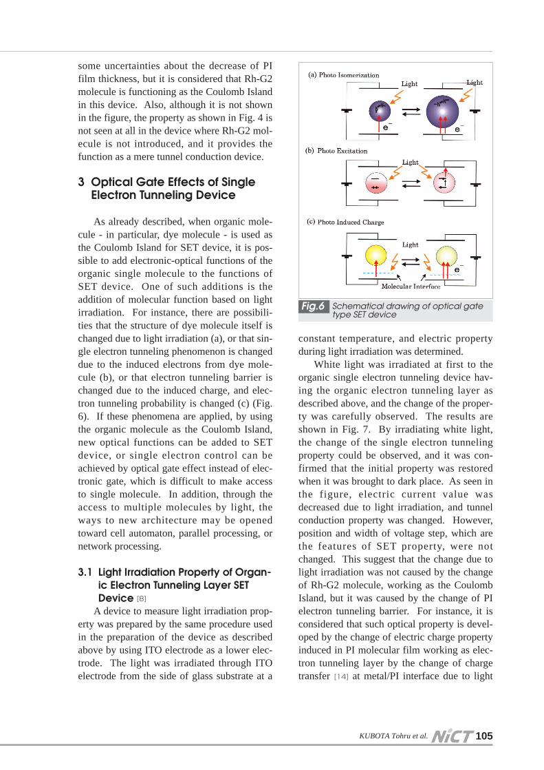
As already described, when organic mole-cule - in particular, dye molecule - is used asthe Coulomb Island for SET device, it is pos-sible to add electronic-optical functions of theorganic single molecule to the functions ofSET device. One of such additions is theaddition of molecular function based on lightirradiation. For instance, there are possibili-ties that the structure of dye molecule itself ischanged due to light irradiation (a), or that sin-gle electron tunneling phenomenon is changeddue to the induced electrons from dye mole-cule (b), or that electron tunneling barrier ischanged due to the induced charge, and elec-tron tunneling probability is changed (c) (Fig.6). If these phenomena are applied, by usingthe organic molecule as the Coulomb Island,new optical functions can be added to SETdevice, or single electron control can beachieved by optical gate effect instead of elec-tronic gate, which is difficult to make accessto single molecule. In addition, through theaccess to multiple molecules by light, theways to new architecture may be openedtoward cell automaton, parallel processing, ornetwork processing.
3.1 Light Irradiation Property of Organ-ic Electron Tunneling Layer SETDevice [8]
A device to measure light irradiation prop-erty was prepared by the same procedure usedin the preparation of the device as describedabove by using ITO electrode as a lower elec-trode. The light was irradiated through ITOelectrode from the side of glass substrate at a
constant temperature, and electric propertyduring light irradiation was determined.
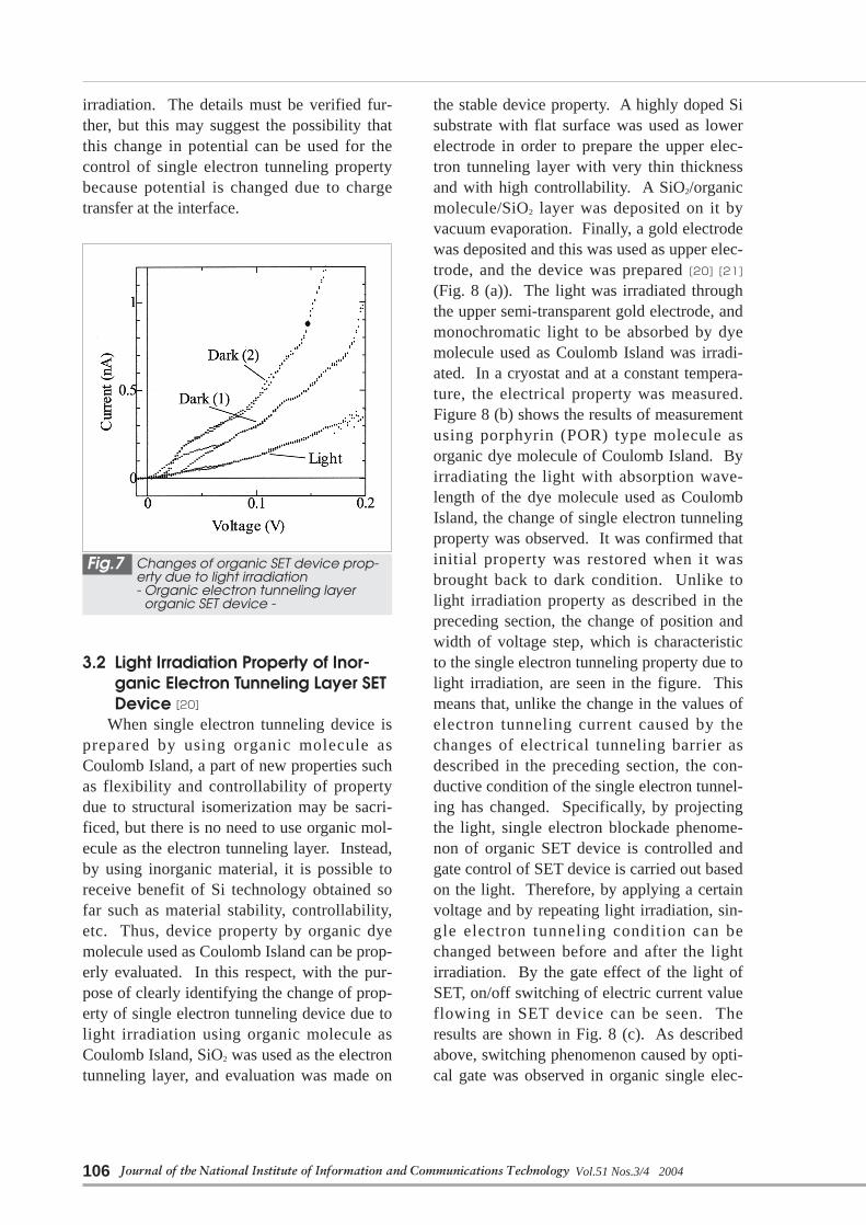
White light was irradiated at first to theorganic single electron tunneling device hav-ing the organic electron tunneling layer asdescribed above, and the change of the proper-ty was carefully observed. The results areshown in Fig. 7. By irradiating white light,the change of the single electron tunnelingproperty could be observed, and it was con-firmed that the initial property was restoredwhen it was brought to dark place. As seen inthe figure, electric current value wasdecreased due to light irradiation, and tunnelconduction property was changed. However,position and width of voltage step, which arethe features of SET property, were notchanged. This suggest that the change due tolight irradiation was not caused by the changeof Rh-G2 molecule, working as the CoulombIsland, but it was caused by the change of PIelectron tunneling barrier. For instance, it isconsidered that such optical property is devel-oped by the change of electric charge propertyinduced in PI molecular film working as elec-tron tunneling layer by the change of chargetransfer [14] at metal/PI interface due to light
KUBOTA Tohru et al. 105
Schematical drawing of optical gatetype SET device
Fig.6
106
irradiation. The details must be verified fur-ther, but this may suggest the possibility thatthis change in potential can be used for thecontrol of single electron tunneling propertybecause potential is changed due to chargetransfer at the interface.
3.2 Light Irradiation Property of Inor-ganic Electron Tunneling Layer SETDevice [20]
When single electron tunneling device isprepared by using organic molecule asCoulomb Island, a part of new properties suchas flexibility and controllability of propertydue to structural isomerization may be sacri-ficed, but there is no need to use organic mol-ecule as the electron tunneling layer. Instead,by using inorganic material, it is possible toreceive benefit of Si technology obtained sofar such as material stability, controllability,etc. Thus, device property by organic dyemolecule used as Coulomb Island can be prop-erly evaluated. In this respect, with the pur-pose of clearly identifying the change of prop-erty of single electron tunneling device due tolight irradiation using organic molecule asCoulomb Island, SiO2 was used as the electrontunneling layer, and evaluation was made on
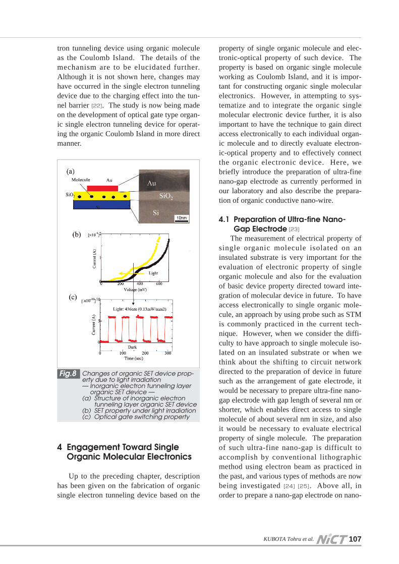
the stable device property. A highly doped Sisubstrate with flat surface was used as lowerelectrode in order to prepare the upper elec-tron tunneling layer with very thin thicknessand with high controllability. A SiO2/organicmolecule/SiO2 layer was deposited on it byvacuum evaporation. Finally, a gold electrodewas deposited and this was used as upper elec-trode, and the device was prepared [20] [21](Fig. 8 (a)). The light was irradiated throughthe upper semi-transparent gold electrode, andmonochromatic light to be absorbed by dyemolecule used as Coulomb Island was irradi-ated. In a cryostat and at a constant tempera-ture, the electrical property was measured.Figure 8 (b) shows the results of measurementusing porphyrin (POR) type molecule asorganic dye molecule of Coulomb Island. Byirradiating the light with absorption wave-length of the dye molecule used as CoulombIsland, the change of single electron tunnelingproperty was observed. It was confirmed thatinitial property was restored when it wasbrought back to dark condition. Unlike tolight irradiation property as described in thepreceding section, the change of position andwidth of voltage step, which is characteristicto the single electron tunneling property due tolight irradiation, are seen in the figure. Thismeans that, unlike the change in the values ofelectron tunneling current caused by thechanges of electrical tunneling barrier asdescribed in the preceding section, the con-ductive condition of the single electron tunnel-ing has changed. Specifically, by projectingthe light, single electron blockade phenome-non of organic SET device is controlled andgate control of SET device is carried out basedon the light. Therefore, by applying a certainvoltage and by repeating light irradiation, sin-gle electron tunneling condition can bechanged between before and after the lightirradiation. By the gate effect of the light ofSET, on/off switching of electric current valueflowing in SET device can be seen. Theresults are shown in Fig. 8 (c). As describedabove, switching phenomenon caused by opti-cal gate was observed in organic single elec-
Journal of the National Institute of Information and Communications Technology Vol.51 Nos.3/4 2004
Changes of organic SET device prop-erty due to light irradiation- Organic electron tunneling layer
organic SET device -
Fig.7
tron tunneling device using organic moleculeas the Coulomb Island. The details of themechanism are to be elucidated further.Although it is not shown here, changes mayhave occurred in the single electron tunnelingdevice due to the charging effect into the tun-nel barrier [22]. The study is now being madeon the development of optical gate type organ-ic single electron tunneling device for operat-ing the organic Coulomb Island in more directmanner.
4 Engagement Toward SingleOrganic Molecular Electronics
Up to the preceding chapter, descriptionhas been given on the fabrication of organicsingle electron tunneling device based on the
property of single organic molecule and elec-tronic-optical property of such device. Theproperty is based on organic single moleculeworking as Coulomb Island, and it is impor-tant for constructing organic single molecularelectronics. However, in attempting to sys-tematize and to integrate the organic singlemolecular electronic device further, it is alsoimportant to have the technique to gain directaccess electronically to each individual organ-ic molecule and to directly evaluate electron-ic-optical property and to effectively connectthe organic electronic device. Here, webriefly introduce the preparation of ultra-finenano-gap electrode as currently performed inour laboratory and also describe the prepara-tion of organic conductive nano-wire.
4.1 Preparation of Ultra-fine Nano-Gap Electrode [23]
The measurement of electrical property ofsingle organic molecule isolated on aninsulated substrate is very important for theevaluation of electronic property of singleorganic molecule and also for the evaluationof basic device property directed toward inte-gration of molecular device in future. To haveaccess electronically to single organic mole-cule, an approach by using probe such as STMis commonly practiced in the current tech-nique. However, when we consider the diffi-culty to have approach to single molecule iso-lated on an insulated substrate or when wethink about the shifting to circuit networkdirected to the preparation of device in futuresuch as the arrangement of gate electrode, itwould be necessary to prepare ultra-fine nano-gap electrode with gap length of several nm orshorter, which enables direct access to singlemolecule of about several nm in size, and alsoit would be necessary to evaluate electricalproperty of single molecule. The preparationof such ultra-fine nano-gap is difficult toaccomplish by conventional lithographicmethod using electron beam as practiced inthe past, and various types of methods are nowbeing investigated [24] [25]. Above all, inorder to prepare a nano-gap electrode on nano-
KUBOTA Tohru et al. 107
Changes of organic SET device prop-erty due to light irradiation — Inorganic electron tunneling layer
organic SET device —(a) Structure of inorganic electron
tunneling layer organic SET device(b) SET property under light irradiation(c) Optical gate switching property
Fig.8
108
meter level, which is in steady state and showsgood reproducibility, we successfully devel-oped a new process using the focusing ionbeam (FIB) system and prepared nano-gap Auelectrode of several nm in width on a SiO2
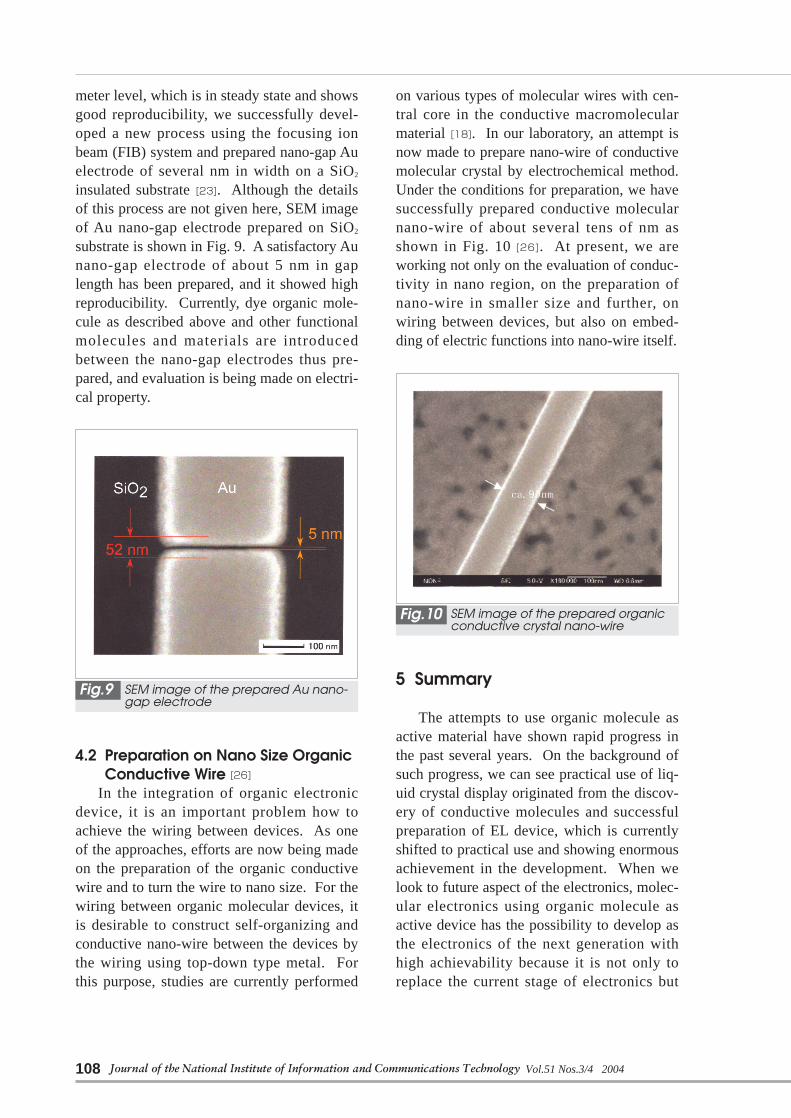
insulated substrate [23]. Although the detailsof this process are not given here, SEM imageof Au nano-gap electrode prepared on SiO2
substrate is shown in Fig. 9. A satisfactory Aunano-gap electrode of about 5 nm in gaplength has been prepared, and it showed highreproducibility. Currently, dye organic mole-cule as described above and other functionalmolecules and materials are introducedbetween the nano-gap electrodes thus pre-pared, and evaluation is being made on electri-cal property.
4.2 Preparation on Nano Size OrganicConductive Wire [26]
In the integration of organic electronicdevice, it is an important problem how toachieve the wiring between devices. As oneof the approaches, efforts are now being madeon the preparation of the organic conductivewire and to turn the wire to nano size. For thewiring between organic molecular devices, itis desirable to construct self-organizing andconductive nano-wire between the devices bythe wiring using top-down type metal. Forthis purpose, studies are currently performed
on various types of molecular wires with cen-tral core in the conductive macromolecularmaterial [18]. In our laboratory, an attempt isnow made to prepare nano-wire of conductivemolecular crystal by electrochemical method.Under the conditions for preparation, we havesuccessfully prepared conductive molecularnano-wire of about several tens of nm asshown in Fig. 10 [26]. At present, we areworking not only on the evaluation of conduc-tivity in nano region, on the preparation ofnano-wire in smaller size and further, onwiring between devices, but also on embed-ding of electric functions into nano-wire itself.
5 Summary
The attempts to use organic molecule asactive material have shown rapid progress inthe past several years. On the background ofsuch progress, we can see practical use of liq-uid crystal display originated from the discov-ery of conductive molecules and successfulpreparation of EL device, which is currentlyshifted to practical use and showing enormousachievement in the development. When welook to future aspect of the electronics, molec-ular electronics using organic molecule asactive device has the possibility to develop asthe electronics of the next generation withhigh achievability because it is not only toreplace the current stage of electronics but
Journal of the National Institute of Information and Communications Technology Vol.51 Nos.3/4 2004
SEM image of the prepared Au nano-gap electrode
Fig.9
SEM image of the prepared organicconductive crystal nano-wire
Fig.10
also because molecular device is cited in theroad map of semiconductor device [27]. Fur-ther, new molecular materials such as nano-tube, fullerene, dendrimer, etc. have beendetected, and proposal and trial production aresuccessively made on new functional devicessuch as molecular photonic device and bio-functional molecular device. It will be devel-oped to molecular electronics, which wouldinclude not only the technique to control mol-ecules and to draw out the properties specificto molecule but also the quantum effect basedon ultra-fine molecular size. We can see sev-eral pioneer studies, including the studies on
single molecular operation, self-organizing,molecular wire, single molecular rectifyingdevice, single molecular light emitting device,molecular FET, molecular transistor, etc. TheSET device using organic single molecule asintroduced in the present report may be one ofsuch subjects of the studies. It is expected thatthe molecular device thus prepared will besystematized together with the results of otherstudies and would act as a part of the organicmolecular devices, which would play animportant role in the field of information andcommunication in future.
KUBOTA Tohru et al. 109
References1 A. Aviram and M. A. Ratner, Chem. Phys. Lett. 29, p.277, 1974.
2 J. Park et al., Nature 417, pp.722-724, 2002.
3 W. Liang et al., Nature 417, pp.725-729, 2002.
4 S. Kubatkin et al., Nature 425, pp.698-701, 2003.
5 Konstantin K. Likharev, Proceedings of the IEEE, Vol,87, p.606, 1999.
6 K. Yano et al., Proceedings of the IEEE, Vol,87, p.633, 1999.
7 T. Kubota and S. Mashiko: Manuscript for the 59th Conference of Applied Physics Society of Japan; 18a-
YH-1, 1998.
8 T. Kubota et al., Technical Report at IEICE, Vol.99, No.292, OME99-69 pp.31-36, 1999.
9 T. Kubota et al., Proceedings of LB9 Conference, Potsdam, p.177, 2000.
10 T. Kubota et al., Thin Solid Films, 393, pp.379-382, 2001.
11 J. Haruyama: “General Theory of Single electron tunneling”; Corona Publishing Co., 2002.
12 Janos H. Fendler: “Nanoparticles and Nanostructured Films”, WILEY-VCH, Weinheim, Chap.15.
13 M. Iwamoto, T. Kubota, and M. Sekine, J.Phys.D 23, p575, 1990.
14 M. Kakimoto et al., Chem.Lett., pp.823-826, 1986.
15 S. Yokoyama, T. Nakahama, A. Otomo, and S. Mashiko, Chem. Lett., p1137, 1997.
16 Y.Noguch, et al., IEICE Trans. Electron., E85-C, 1247, 2002.
17 T. Kubota et al., Thin Solid Films, 210/21, p277, 1992.
18 E. Itoh and M. Iwamoto, Appl.Phys.Lett. 68, 2734, 1996.
19 E. Itoh, Y. Niwa, and M. Iwamoto, Thin Solid Films, 284, 545, 1996.
20 Y. Wakayama et al., Appl.Phys.Lett. Vol.85, No.2, p.329, 2004.
21 Y.Wakayama et al., J.Appl.Phys. Vol.94, No.7, p.4711, 2003.
22 Y.Noguchi et al., in preparation.
23 T.Nagase et al., Thin Solid Films 438/439, p.374, 2003.
24 H.Park et al., Appl.Phys.Lett. Vol.75, p.301, 1999.
25 A.F.Morpurgo et al., Appl.Phys.Lett. Vol.75, p.2084, 1999.
26 H. Hasegawa et al., Thin Solid Films 438/439, p.352, 2003.
27 International Road Map ITRS 2001 http:://public.itrs.net

110 Journal of the National Institute of Information and Communications Technology Vol.51 Nos.3/4 2004
KUBOTA Tohru, Dr.Eng.
Senior Researcher, NanotechnologyGroup, Kansai Advanced ResearchCenter, Basic and Advanced ResearchDepartment
Molecular Electronics
NAGASE Takashi, Dr.Eng.
Expert Researcher, NanotechnologyGroup, Kansai Advanced ResearchCenter, Basic and Advanced ResearchDepartment
Molecular Electronics
HASEGAWA Hiroyuki, Ph.D.
Senior Researcher, NanotechnologyGroup, Kansai Advanced ResearchCenter, Basic and Advanced ResearchDepartment
Materials Science
MASHIKO Shinro, Dr.Eng.
Director of Kansai Advanced ResearchCenter, Basic and Advanced ResearchDepartment
Laser Spectroscopy, Nanotechnology