Embed Size (px)
Citation preview
freescale.com
3PHACBLDCHVPSUGRev. 101/2007
Users Guide
3-Phase AC/BLDC High Voltage Power Stage Board

3-Phase AC/BLDC High-Voltage, Power-Stage BoardUsers Guide
by: Petr FrgalFreescale SemiconductorCzech System Center
To provide the most up-to-date information, the revision of our documents on the World Wide Web will be the most current. Your printed copy may be an earlier revision. To verify that you have the latest information available, refer to http://www.freescale.comThe following revision history table summarises changes contained in this document. For your convenience, the page number designators have been linked to the appropriate location.
Revision History
Date RevisionLevel Description Page
Number(s)
01/2006 0 Initial release N/A
01/2007 1 After MCD team revision 70
3-Phase AC/BLDC High-Voltage, Power-Stage Board, Rev. 1
Freescale Semiconductor 3

3-Phase AC/BLDC High-Voltage, Power-Stage Board, Rev. 1
4 Freescale Semiconductor
List of Figures
Figure 1-1 System Configurations . . . . . . . . . . . . . . . . . . . . . . . . . . . . . . . . . . . . . . . . . . . . . . . . . . . 12Figure 1-2 3-phase AC/BLDC High-Voltage Power Stage. . . . . . . . . . . . . . . . . . . . . . . . . . . . . . . . . 13Figure 1-3 3-phase AC/BLDC High-Voltage Power Stage Setup Without External PFC. . . . . . . . . . 15Figure 2-1 Block Diagram . . . . . . . . . . . . . . . . . . . . . . . . . . . . . . . . . . . . . . . . . . . . . . . . . . . . . . . . . 18Figure 3-1 40-Pin Connector J8. . . . . . . . . . . . . . . . . . . . . . . . . . . . . . . . . . . . . . . . . . . . . . . . . . . . . 27Figure 4-1 Phase Output . . . . . . . . . . . . . . . . . . . . . . . . . . . . . . . . . . . . . . . . . . . . . . . . . . . . . . . . . . 31Figure 4-2 Bus Feedback. . . . . . . . . . . . . . . . . . . . . . . . . . . . . . . . . . . . . . . . . . . . . . . . . . . . . . . . . . 33Figure 4-3 Current Range - Board Detail . . . . . . . . . . . . . . . . . . . . . . . . . . . . . . . . . . . . . . . . . . . . . . 34Figure 4-4 Temperature Sensing Circuit and Linearisation Chart . . . . . . . . . . . . . . . . . . . . . . . . . . . 35Figure 4-5 Back EMF sensing . . . . . . . . . . . . . . . . . . . . . . . . . . . . . . . . . . . . . . . . . . . . . . . . . . . . . . 36Figure 4-6 Phase Current Sensing . . . . . . . . . . . . . . . . . . . . . . . . . . . . . . . . . . . . . . . . . . . . . . . . . . 37Figure 4-7 Brake . . . . . . . . . . . . . . . . . . . . . . . . . . . . . . . . . . . . . . . . . . . . . . . . . . . . . . . . . . . . . . . . 38Figure 4-8 LED Indication . . . . . . . . . . . . . . . . . . . . . . . . . . . . . . . . . . . . . . . . . . . . . . . . . . . . . . . . . 41Figure 4-9 DC Bus Power Supply . . . . . . . . . . . . . . . . . . . . . . . . . . . . . . . . . . . . . . . . . . . . . . . . . . . 42Figure 4-10 +18V Power Supply . . . . . . . . . . . . . . . . . . . . . . . . . . . . . . . . . . . . . . . . . . . . . . . . . . . . . 43Figure 4-11 +15V_A Power Supply . . . . . . . . . . . . . . . . . . . . . . . . . . . . . . . . . . . . . . . . . . . . . . . . . . . 43Figure 4-12 +5V_D Power Supply . . . . . . . . . . . . . . . . . . . . . . . . . . . . . . . . . . . . . . . . . . . . . . . . . . . . 44Figure 4-13 +3.3V/+5V_A Power Supply . . . . . . . . . . . . . . . . . . . . . . . . . . . . . . . . . . . . . . . . . . . . . . . 44Figure 4-14 Analogue Sensing Range - Board Detail . . . . . . . . . . . . . . . . . . . . . . . . . . . . . . . . . . . . . 45Figure 4-15 +12V_Fan Power Supply . . . . . . . . . . . . . . . . . . . . . . . . . . . . . . . . . . . . . . . . . . . . . . . . . 46Figure 4-16 Voltage Reference . . . . . . . . . . . . . . . . . . . . . . . . . . . . . . . . . . . . . . . . . . . . . . . . . . . . . . 46Figure A-1 Power Stage Overview . . . . . . . . . . . . . . . . . . . . . . . . . . . . . . . . . . . . . . . . . . . . . . . . . . . 48Figure A-2 Phase Current Sensing . . . . . . . . . . . . . . . . . . . . . . . . . . . . . . . . . . . . . . . . . . . . . . . . . . 49Figure A-3 Back EMF Sensing . . . . . . . . . . . . . . . . . . . . . . . . . . . . . . . . . . . . . . . . . . . . . . . . . . . . . . 50Figure A-4 IGBT Drivers. . . . . . . . . . . . . . . . . . . . . . . . . . . . . . . . . . . . . . . . . . . . . . . . . . . . . . . . . . . 51Figure A-5 3-Phase Power Bridge . . . . . . . . . . . . . . . . . . . . . . . . . . . . . . . . . . . . . . . . . . . . . . . . . . . 52Figure A-6 DC bus Power Supply . . . . . . . . . . . . . . . . . . . . . . . . . . . . . . . . . . . . . . . . . . . . . . . . . . . 53Figure A-7 Power Supplies. . . . . . . . . . . . . . . . . . . . . . . . . . . . . . . . . . . . . . . . . . . . . . . . . . . . . . . . . 54Figure C-1 Power Stage Board Top Layer . . . . . . . . . . . . . . . . . . . . . . . . . . . . . . . . . . . . . . . . . . . . . 62Figure C-2 Power Stage Board Bottom Layer . . . . . . . . . . . . . . . . . . . . . . . . . . . . . . . . . . . . . . . . . . 63Figure C-3 Power Stage Board Inner 1 Layer . . . . . . . . . . . . . . . . . . . . . . . . . . . . . . . . . . . . . . . . . . 64Figure C-4 Power Stage Board Inner 2 Layer . . . . . . . . . . . . . . . . . . . . . . . . . . . . . . . . . . . . . . . . . . 65Figure C-5 Power Stage Board Silkscreen Top Layer . . . . . . . . . . . . . . . . . . . . . . . . . . . . . . . . . . . . 66Figure C-6 Power Stage Board Silkscreen Bottom Layer . . . . . . . . . . . . . . . . . . . . . . . . . . . . . . . . . 67
3-Phase AC/BLDC High Voltage Power Stage Board, Rev. 1
Freescale Semiconductor 5

3-Phase AC/BLDC High Voltage Power Stage Board, Rev. 1
6 Freescale Semiconductor
Table of Contents
Chapter 1 Introduction
1.1 Contents. . . . . . . . . . . . . . . . . . . . . . . . . . . . . . . . . . . . . . . . . . . . . . . . . . . . . . . . . . . . . . . . . . . 111.2 3-Phase AC/BLDC High Voltage Power Stage Outline . . . . . . . . . . . . . . . . . . . . . . . . . . . . . . . 111.3 About this Manual . . . . . . . . . . . . . . . . . . . . . . . . . . . . . . . . . . . . . . . . . . . . . . . . . . . . . . . . . . . 111.4 Warnings . . . . . . . . . . . . . . . . . . . . . . . . . . . . . . . . . . . . . . . . . . . . . . . . . . . . . . . . . . . . . . . . . . 131.5 Setup Guide . . . . . . . . . . . . . . . . . . . . . . . . . . . . . . . . . . . . . . . . . . . . . . . . . . . . . . . . . . . . . . . . 14
Chapter 2 Operational Description
2.1 Contents. . . . . . . . . . . . . . . . . . . . . . . . . . . . . . . . . . . . . . . . . . . . . . . . . . . . . . . . . . . . . . . . . . . 172.2 Introduction . . . . . . . . . . . . . . . . . . . . . . . . . . . . . . . . . . . . . . . . . . . . . . . . . . . . . . . . . . . . . . . . 172.3 Electrical Characteristics . . . . . . . . . . . . . . . . . . . . . . . . . . . . . . . . . . . . . . . . . . . . . . . . . . . . . . 182.4 Fuse replacement . . . . . . . . . . . . . . . . . . . . . . . . . . . . . . . . . . . . . . . . . . . . . . . . . . . . . . . . . . . 19
Chapter 3 Pin Description
3.1 Contents. . . . . . . . . . . . . . . . . . . . . . . . . . . . . . . . . . . . . . . . . . . . . . . . . . . . . . . . . . . . . . . . . . . 213.2 Introduction . . . . . . . . . . . . . . . . . . . . . . . . . . . . . . . . . . . . . . . . . . . . . . . . . . . . . . . . . . . . . . . . 213.3 Signal Descriptions . . . . . . . . . . . . . . . . . . . . . . . . . . . . . . . . . . . . . . . . . . . . . . . . . . . . . . . . . . 213.3.1 Fan Terminal J1 . . . . . . . . . . . . . . . . . . . . . . . . . . . . . . . . . . . . . . . . . . . . . . . . . . . . . . . . . . 223.3.2 PFC Signals Connector J2 and PFC POWER Connectors J5 and J11 . . . . . . . . . . . . . . . . 223.3.3 Jumper Terminals J3 and J7 . . . . . . . . . . . . . . . . . . . . . . . . . . . . . . . . . . . . . . . . . . . . . . . . 233.3.4 Brake Resistor Connector J4 . . . . . . . . . . . . . . . . . . . . . . . . . . . . . . . . . . . . . . . . . . . . . . . . 243.3.5 Motor Connector J6 . . . . . . . . . . . . . . . . . . . . . . . . . . . . . . . . . . . . . . . . . . . . . . . . . . . . . . . 243.3.6 UNI-3 Connector J8 . . . . . . . . . . . . . . . . . . . . . . . . . . . . . . . . . . . . . . . . . . . . . . . . . . . . . . . 243.3.7 Line Input Connector J9 . . . . . . . . . . . . . . . . . . . . . . . . . . . . . . . . . . . . . . . . . . . . . . . . . . . . 273.3.8 Earth Ground Terminal J10 . . . . . . . . . . . . . . . . . . . . . . . . . . . . . . . . . . . . . . . . . . . . . . . . . 283.3.9 External -15V_A jumper J12 . . . . . . . . . . . . . . . . . . . . . . . . . . . . . . . . . . . . . . . . . . . . . . . . 28
Chapter 4 Design Consideration
4.1 Contents. . . . . . . . . . . . . . . . . . . . . . . . . . . . . . . . . . . . . . . . . . . . . . . . . . . . . . . . . . . . . . . . . . . 294.2 Overview . . . . . . . . . . . . . . . . . . . . . . . . . . . . . . . . . . . . . . . . . . . . . . . . . . . . . . . . . . . . . . . . . . 294.3 3-phase Bridge. . . . . . . . . . . . . . . . . . . . . . . . . . . . . . . . . . . . . . . . . . . . . . . . . . . . . . . . . . . . . . 294.4 Bus Voltage and Current Feedback. . . . . . . . . . . . . . . . . . . . . . . . . . . . . . . . . . . . . . . . . . . . . . 324.5 Over-current and Undervoltage Functions. . . . . . . . . . . . . . . . . . . . . . . . . . . . . . . . . . . . . . . . . 344.6 Temperature Sensing . . . . . . . . . . . . . . . . . . . . . . . . . . . . . . . . . . . . . . . . . . . . . . . . . . . . . . . . 344.7 Back EMF Signals . . . . . . . . . . . . . . . . . . . . . . . . . . . . . . . . . . . . . . . . . . . . . . . . . . . . . . . . . . . 35
3-Phase AC/BLDC High Voltage Power Stage Board*, Rev. 1
Freescale Semiconductor 7
4.8 Phase Current Sensing . . . . . . . . . . . . . . . . . . . . . . . . . . . . . . . . . . . . . . . . . . . . . . . . . . . . . . . 364.9 Brake . . . . . . . . . . . . . . . . . . . . . . . . . . . . . . . . . . . . . . . . . . . . . . . . . . . . . . . . . . . . . . . . . . . . . 374.10 External Power Factor Correction . . . . . . . . . . . . . . . . . . . . . . . . . . . . . . . . . . . . . . . . . . . . . . . 384.11 Test Points and LED Indication . . . . . . . . . . . . . . . . . . . . . . . . . . . . . . . . . . . . . . . . . . . . . . . . . 384.12 Power Supplies and Voltage Reference . . . . . . . . . . . . . . . . . . . . . . . . . . . . . . . . . . . . . . . . . . 424.12.1 Input Power Supply . . . . . . . . . . . . . . . . . . . . . . . . . . . . . . . . . . . . . . . . . . . . . . . . . . . . . . . 424.12.2 +18V Power Supply . . . . . . . . . . . . . . . . . . . . . . . . . . . . . . . . . . . . . . . . . . . . . . . . . . . . . . . 424.12.3 +15V_A Power Supply . . . . . . . . . . . . . . . . . . . . . . . . . . . . . . . . . . . . . . . . . . . . . . . . . . . . . 434.12.4 +5V_D Power Supply. . . . . . . . . . . . . . . . . . . . . . . . . . . . . . . . . . . . . . . . . . . . . . . . . . . . . . 434.12.5 +3.3V_A/+5V_A Power Supply . . . . . . . . . . . . . . . . . . . . . . . . . . . . . . . . . . . . . . . . . . . . . . 444.12.6 +12V_Fan Power Supply . . . . . . . . . . . . . . . . . . . . . . . . . . . . . . . . . . . . . . . . . . . . . . . . . . . 454.12.7 +1.65V/2.5V Reference . . . . . . . . . . . . . . . . . . . . . . . . . . . . . . . . . . . . . . . . . . . . . . . . . . . . 46
Appendix A. 3-phase AC/BLDC High Voltage Power Stage Board Schematics
Appendix B.Bill of Materials
Appendix C. 3-phase AC/BLDC High Voltage Power Stage Board
Layouts
3-Phase AC/BLDC High Voltage Power Stage Board*, Rev. 1
8 Freescale Semiconductor
List of TablesTable 2-1 Electrical Characteristics. . . . . . . . . . . . . . . . . . . . . . . . . . . . . . . . . . . . . . . . . . . . . . . . . . . 19Table 3-1 Connector J2 Signal Descriptions. . . . . . . . . . . . . . . . . . . . . . . . . . . . . . . . . . . . . . . . . . . . 22Table 3-2 PFC POWER Connector J5 Descriptions . . . . . . . . . . . . . . . . . . . . . . . . . . . . . . . . . . . . . 23Table 3-3 PFC POWER Connector J11 Descriptions . . . . . . . . . . . . . . . . . . . . . . . . . . . . . . . . . . . . 23Table 3-4 Jumper J3 Setting Descriptions . . . . . . . . . . . . . . . . . . . . . . . . . . . . . . . . . . . . . . . . . . . . . 23Table 3-5 Jumper J7 Setting Descriptions . . . . . . . . . . . . . . . . . . . . . . . . . . . . . . . . . . . . . . . . . . . . . 24Table 3-6 Connector J6 Signal Descriptions. . . . . . . . . . . . . . . . . . . . . . . . . . . . . . . . . . . . . . . . . . . . 24Table 3-7 Connector J8 Signal Descriptions. . . . . . . . . . . . . . . . . . . . . . . . . . . . . . . . . . . . . . . . . . . . 25Table B-1 Parts List . . . . . . . . . . . . . . . . . . . . . . . . . . . . . . . . . . . . . . . . . . . . . . . . . . . . . . . . . . . . . . . 57
3-Phase AC/BLDC High Voltage Power Stage Board, Rev. 1
Freescale Semiconductor 9

3-Phase AC/BLDC High Voltage Power Stage Board, Rev. 1
10 Freescale Semiconductor
Chapter 1 Introduction
1.1 Contents1.2 3-Phase AC/BLDC High Voltage Power Stage Outline . . . . . . . . . . . . . . . 111.3 About this Manual . . . . . . . . . . . . . . . . . . . . . . . . . . . . . . . . . . . . . . . . . . . 111.4 Warnings . . . . . . . . . . . . . . . . . . . . . . . . . . . . . . . . . . . . . . . . . . . . . . . . . . 131.5 Setup Guide . . . . . . . . . . . . . . . . . . . . . . . . . . . . . . . . . . . . . . . . . . . . . . . . 14
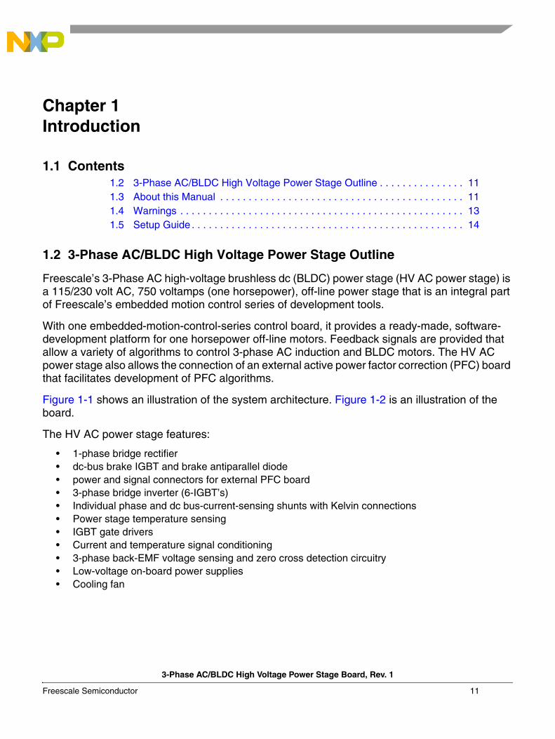
1.2 3-Phase AC/BLDC High Voltage Power Stage Outline
Freescale’s 3-Phase AC high-voltage brushless dc (BLDC) power stage (HV AC power stage) is a 115/230 volt AC, 750 voltamps (one horsepower), off-line power stage that is an integral part of Freescale’s embedded motion control series of development tools.
With one embedded-motion-control-series control board, it provides a ready-made, software-development platform for one horsepower off-line motors. Feedback signals are provided that allow a variety of algorithms to control 3-phase AC induction and BLDC motors. The HV AC power stage also allows the connection of an external active power factor correction (PFC) board that facilitates development of PFC algorithms.
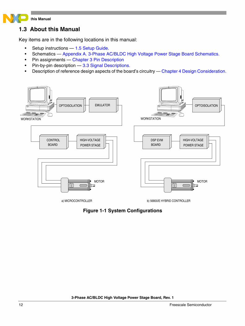
Figure 1-1 shows an illustration of the system architecture. Figure 1-2 is an illustration of the board.
The HV AC power stage features:
• 1-phase bridge rectifier• dc-bus brake IGBT and brake antiparallel diode• power and signal connectors for external PFC board• 3-phase bridge inverter (6-IGBT’s)• Individual phase and dc bus-current-sensing shunts with Kelvin connections• Power stage temperature sensing• IGBT gate drivers• Current and temperature signal conditioning• 3-phase back-EMF voltage sensing and zero cross detection circuitry• Low-voltage on-board power supplies• Cooling fan
3-Phase AC/BLDC High Voltage Power Stage Board, Rev. 1
Freescale Semiconductor 11
About this Manual
1.3 About this Manual
Key items are in the following locations in this manual:
• Setup instructions — 1.5 Setup Guide.• Schematics — Appendix A. 3-Phase AC/BLDC High Voltage Power Stage Board Schematics.• Pin assignments — Chapter 3 Pin Description• Pin-by-pin description — 3.3 Signal Descriptions.• Description of reference design aspects of the board’s circuitry — Chapter 4 Design Consideration.
Figure 1-1 System Configurations
EMULATOR
MOTOR
WORKSTATION
OPTOISOLATION OPTOISOLATION
MOTOR
WORKSTATION
b) 56800/E HYBRID CONTROLLERa) MICROCONTROLLER
CONTROL BOARD
HIGH-VOLTAGE
POWER STAGE
DSP EVM BOARD
HIGH-VOLTAGE
POWER STAGE
3-Phase AC/BLDC High Voltage Power Stage Board, Rev. 1
12 Freescale Semiconductor
Warnings
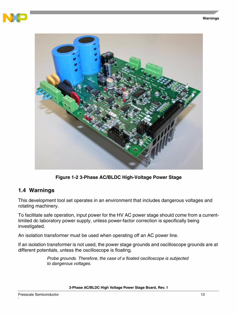
Figure 1-2 3-Phase AC/BLDC High-Voltage Power Stage
1.4 Warnings
This development tool set operates in an environment that includes dangerous voltages and rotating machinery.
To facilitate safe operation, input power for the HV AC power stage should come from a current-limited dc laboratory power supply, unless power-factor correction is specifically being investigated.
An isolation transformer must be used when operating off an AC power line.
If an isolation transformer is not used, the power stage grounds and oscilloscope grounds are at different potentials, unless the oscilloscope is floating.
Probe grounds. Therefore, the case of a floated oscilloscope is subjected to dangerous voltages.
3-Phase AC/BLDC High Voltage Power Stage Board, Rev. 1
Freescale Semiconductor 13‘
Setup Guide
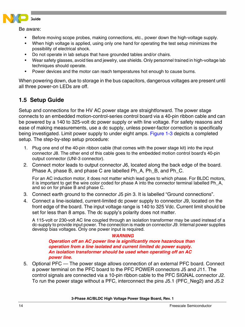
Be aware:
• Before moving scope probes, making connections, etc., power down the high-voltage supply.• When high voltage is applied, using only one hand for operating the test setup minimizes the
possibility of electrical shock.• Do not operate in lab setups that have grounded tables and/or chairs.• Wear safety glasses, avoid ties and jewelry, use shields. Only personnel trained in high-voltage lab
techniques should operate.• Power devices and the motor can reach temperatures hot enough to cause burns.
When powering down, due to storage in the bus capacitors, dangerous voltages are present until all three power-on LEDs are off.
1.5 Setup Guide
Setup and connections for the HV AC power stage are straightforward. The power stage connects to an embedded motion-control-series control board via a 40-pin ribbon cable and can be powered by a 140 to 325-volt dc power supply or with line voltage. For safety reasons and ease of making measurements, use a dc supply, unless power-factor correction is specifically being investigated. Limit power supply to under eight amps. Figure 1-3 depicts a completed setup. The step-by-step setup procedure:
1. Plug one end of the 40-pin ribbon cable (that comes with the power stage kit) into the input connector J8. The other end of this cable goes to the embedded motion control board's 40-pin output connector (UNI-3 connector).
2. Connect motor leads to output connector J6, located along the back edge of the board. Phase A, phase B, and phase C are labelled Ph_A, Ph_B, and Ph_C.
For an AC induction motor, it does not matter which lead goes to which phase. For BLDC motors, it is important to get the wire color coded for phase A into the connector terminal labelled Ph_A, and so on for phase B and phase C.
3. Connect earth ground to the connector J5 pin 3. It is labelled “Ground connections”.4. Connect a line-isolated, current-limited dc power supply to connector J9, located on the
front edge of the board. The input voltage range is 140 to 325 Vdc. Current limit should be set for less than 8 amps. The dc supply’s polarity does not matter.
A 115-volt or 230-volt AC line coupled through an isolation transformer may be used instead of a dc-supply to provide input power. The connection is made on connector J9. Internal power supplies develop bias voltages. Only one power input is required.
WARNINGOperation off an AC power line is significantly more hazardous than operation from a line isolated and current limited dc power supply.An isolation transformer should be used when operating off an AC power line.
5. Optional PFC — The power stage allows connection of an external PFC board. Connect a power terminal on the PFC board to the PFC POWER connectors J5 and J11. The control signals are connected via a 10-pin ribbon cable to the PFC SIGNAL connector J2. To run the power stage without a PFC, interconnect the pins J5.1 (PFC_Neg2) and J5.2
3-Phase AC/BLDC High Voltage Power Stage Board, Rev. 1
14 Freescale Semiconductor

Setup Guide
(PFC_Neg1), J11.1 (PFC_Pos2) and J11.2 (PFC_Pos1) by a power-jumper wires (manufacturer setting).
6. Optional braking resistor — If braking mode is investigated during motor operation, an external resistor must be connected to the connector J4, Brake resistor.
7. Set up the control board. For safety reasons and avoiding damaging the computer, insert any galvanic isolation, as an opto box, between the control board and computer.
8. Apply power to the power stage. All green power-on LEDs (+18V and +5V_D in the center, +12V in the upper left-hand corner) light, and the fan runs when power is present. If the fan does not run, check if the jumper J1 is installed (default setting). The power stage powers the control board.
WARNINGHazardous voltages are present. Re-read all of 1.2 Warnings carefully.
3-Phase AC/BLDC High Voltage Power Stage Board, Rev. 1
Freescale Semiconductor 15‘
Setup Guide
Figure 1-3 3-Phase AC/BLDC High-Voltage Power Stage Setup Without External PFC
Freescale SemiconductorEmbedded Motion Control
Series
J9
Phase_C
Phase_B
Phase_A
Control Board
40-PinRibbon Cable
1 2 3 4 5
Motor
Freescale Semiconductor3-ph. AC/BLDC High Voltage
3
2
1
J6
Hall/EncoderConnector
J8
HALL C / ENCODER INDEX
HALL B / ENCODER PHASE BHALL A / ENCODER PHASE A
GND+5V
140 - 325 Vdc
6
ENCODER HOME
Power Stage
115 - 230 Vac
J4
R brake
J53
2
1
J11
2
1
3-Phase AC/BLDC High Voltage Power Stage Board, Rev. 1
16 Freescale Semiconductor
Chapter 2 Operational Description
2.1 Contents2.2 Introduction . . . . . . . . . . . . . . . . . . . . . . . . . . . . . . . . . . . . . . . . . . . . . . . . 172.3 Electrical Characteristics . . . . . . . . . . . . . . . . . . . . . . . . . . . . . . . . . . . . . . 182.4 Fuse replacement . . . . . . . . . . . . . . . . . . . . . . . . . . . . . . . . . . . . . . . . . . . 19
2.2 Introduction
Freescale’s embedded motion-control series high-voltage (HV) ACAC power stage is a 750-voltamps (one horsepower), 3-phase power stage that will operate off dc input voltages from 140 V to 325 V, and AC line voltages from 100 V to 240 V. With an embedded motion-control-series control boards, it provides a software-development platform that allows algorithms to be written and tested without designing and building a power stage. It supports a variety of algorithms for AC induction and brushless dc (BLDC) motors.
The high-voltage AC-power stage has a printed circuit board. The printed circuit board contains an input rectifier, brake IGBT and diode, bridge IGBTs, IGBT-gate-drive circuits, analog-signal conditioning, low-voltage power supplies, and some large, passive, power components. All power devices that need to dissipate heat and a temperature sensor are mounted on a heatsink situated below the printed circuit board (Figure 1-2).
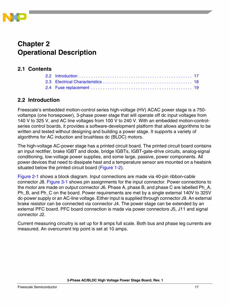
Figure 2-1 shows a block diagram. Input connections are made via 40-pin ribbon-cable connector J8. Figure 3-1 shows pin assignments for the input connector. Power connections to the motor are made on output connector J6. Phase A, phase B, and phase C are labelled Ph_A, Ph_B, and Ph_C on the board. Power requirements are met by a single external 140V to 325V dc-power supply or an AC-line voltage. Either input is supplied through connector J9. An external brake resistor can be connected via connector J4. The power stage can be extended by an external PFC board. PFC board connection is made via power connectors J5, J11 and signal connector J2.
Current measuring circuitry is set up for 8 amps full scale. Both bus and phase leg currents are measured. An overcurrent trip point is set at 10 amps.
3-Phase AC/BLDC High Voltage Power Stage Board, Rev. 1
Freescale Semiconductor 17
Electrical Characteristics
Figure 2-1 Block Diagram
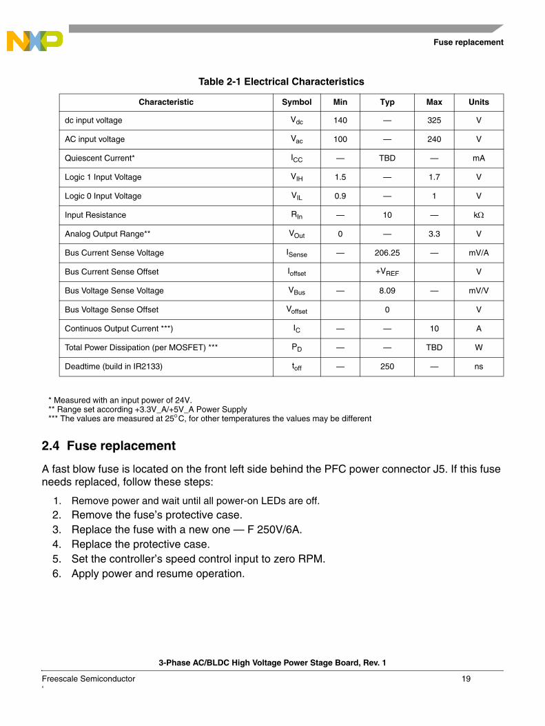
2.3 Electrical Characteristics
The electrical characteristics in Table 2-1 apply to operations at 25°C with a 325-Vdc power- supply voltage.
3-PH IGBTBRIDGE
IGBT DRIVERS
SIGNAL CONDITIONING
INPUT, DC BUS, PHASE voltages and currents,ZERO cross, temperature
BRAKE IGBT+ DIODE
POWERSUPPLY
+15V_D, +5V_D, +15V_A+3.3/5V_A, +12V_FAN
1-PHRECTIFIER
J9
J8
J2
J5 J6 J4
MOTORPFC POWERINPUT
PF
CC
ON
TR
OL
UN
I-3
BRAKE RESISTOR
Legend: Module Connector
J11
3-Phase AC/BLDC High Voltage Power Stage Board, Rev. 1
18 Freescale Semiconductor
Fuse replacement
* Measured with an input power of 24V.** Range set according +3.3V_A/+5V_A Power Supply*** The values are measured at 25°C, for other temperatures the values may be different
2.4 Fuse replacement
A fast blow fuse is located on the front left side behind the PFC power connector J5. If this fuse needs replaced, follow these steps:
1. Remove power and wait until all power-on LEDs are off.2. Remove the fuse’s protective case.3. Replace the fuse with a new one — F 250V/6A.4. Replace the protective case.5. Set the controller’s speed control input to zero RPM.6. Apply power and resume operation.
Table 2-1 Electrical Characteristics
Characteristic Symbol Min Typ Max Units
dc input voltage Vdc 140 — 325 V
AC input voltage Vac 100 — 240 V
Quiescent Current* ICC — TBD — mA
Logic 1 Input Voltage VIH 1.5 — 1.7 V
Logic 0 Input Voltage VIL 0.9 — 1 V
Input Resistance RIn — 10 — kΩ
Analog Output Range** VOut 0 — 3.3 V
Bus Current Sense Voltage ISense — 206.25 — mV/A
Bus Current Sense Offset Ioffset +VREF V
Bus Voltage Sense Voltage VBus — 8.09 — mV/V
Bus Voltage Sense Offset Voffset 0 V
Continuos Output Current ***) IC — — 10 A
Total Power Dissipation (per MOSFET) *** PD — — TBD W
Deadtime (build in IR2133) toff — 250 — ns
3-Phase AC/BLDC High Voltage Power Stage Board, Rev. 1
Freescale Semiconductor 19‘

Fuse replacement
3-Phase AC/BLDC High Voltage Power Stage Board, Rev. 1
20 Freescale Semiconductor
Chapter 3 Pin Description
3.1 Contents3.2 Introduction . . . . . . . . . . . . . . . . . . . . . . . . . . . . . . . . . . . . . . . . . . . . . . . . 213.3 Signal Descriptions . . . . . . . . . . . . . . . . . . . . . . . . . . . . . . . . . . . . . . . . . . 21
3.2 Introduction
Inputs, outputs, and jumper terminals are located on twelve connectors available on the board:
• Fan
• PFC signals
• Jumper J3 and J7
• Brake resistor
• PFC power
• 3-pin motor
• 40-pin UNI-3
• Line input
• Earth ground connection
• External -15V_A jumper
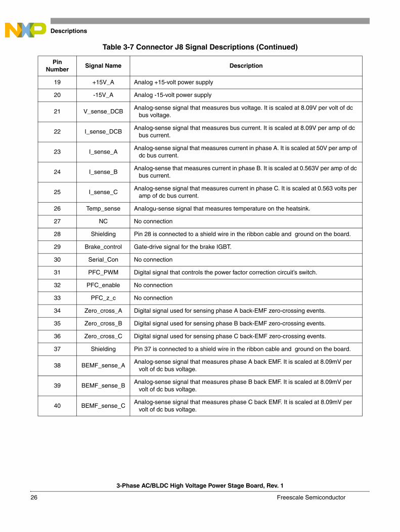
Pin descriptions for each connector and the test points are identified in the following information. Figure 3-1 shows the pin assignments for the UNI-3 connectors. Table 3-7 shows the signal descriptions.
The 3-phase AC/BLDC High-Voltage Power Stage contains several connectors that serve for a connection of a power supply, for motor phases connection, and other functions.
The input power supply attached to the J9 line AC input must not be less than 100V or higher than 230V, or a DC power supply between 140V and 325V.
The output for the motor is done by a 3-way connector J6. See 3.3.5 Motor Connector J6 for more details.
3-Phase AC/BLDC High Voltage Power Stage Board, Rev. 1
Freescale Semiconductor 21
Signal Descriptions
3.3 Signal Descriptions
Pin descriptions are identified in this subsection.
3.3.1 Fan Terminal J1
Cooling efficiency can be increased by using a fan mechanically mounted on a heat-sink. To use a fan, set the jumper plug on Fan Terminal J1.
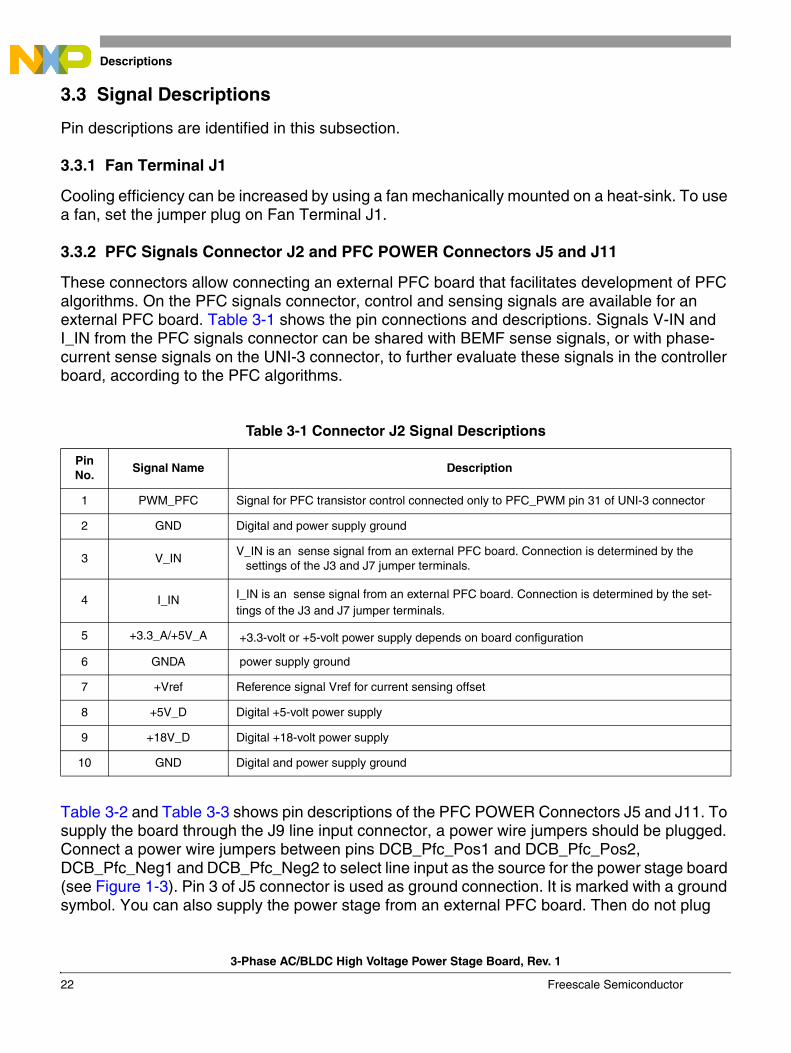
3.3.2 PFC Signals Connector J2 and PFC POWER Connectors J5 and J11
These connectors allow connecting an external PFC board that facilitates development of PFC algorithms. On the PFC signals connector, control and sensing signals are available for an external PFC board. Table 3-1 shows the pin connections and descriptions. Signals V-IN and I_IN from the PFC signals connector can be shared with BEMF sense signals, or with phase- current sense signals on the UNI-3 connector, to further evaluate these signals in the controller board, according to the PFC algorithms.
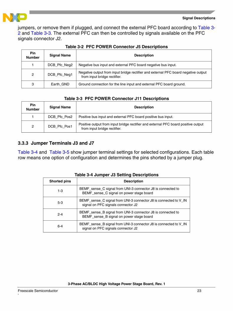
Table 3-2 and Table 3-3 shows pin descriptions of the PFC POWER Connectors J5 and J11. To supply the board through the J9 line input connector, a power wire jumpers should be plugged. Connect a power wire jumpers between pins DCB_Pfc_Pos1 and DCB_Pfc_Pos2, DCB_Pfc_Neg1 and DCB_Pfc_Neg2 to select line input as the source for the power stage board (see Figure 1-3). Pin 3 of J5 connector is used as ground connection. It is marked with a ground symbol. You can also supply the power stage from an external PFC board. Then do not plug
Table 3-1 Connector J2 Signal Descriptions
Pin No.
Signal Name Description
1 PWM_PFC Signal for PFC transistor control connected only to PFC_PWM pin 31 of UNI-3 connector
2 GND Digital and power supply ground
3 V_INV_IN is an sense signal from an external PFC board. Connection is determined by the
settings of the J3 and J7 jumper terminals.
4 I_IN I_IN is an sense signal from an external PFC board. Connection is determined by the set-tings of the J3 and J7 jumper terminals.
5 +3.3_A/+5V_A +3.3-volt or +5-volt power supply depends on board configuration
6 GNDA power supply ground
7 +Vref Reference signal Vref for current sensing offset
8 +5V_D Digital +5-volt power supply
9 +18V_D Digital +18-volt power supply
10 GND Digital and power supply ground
3-Phase AC/BLDC High Voltage Power Stage Board, Rev. 1
22 Freescale Semiconductor
Signal Descriptions
jumpers, or remove them if plugged, and connect the external PFC board according to Table 3-2 and Table 3-3. The external PFC can then be controlled by signals available on the PFC signals connector J2.
Table 3-2 PFC POWER Connector J5 Descriptions
Table 3-3 PFC POWER Connector J11 Descriptions
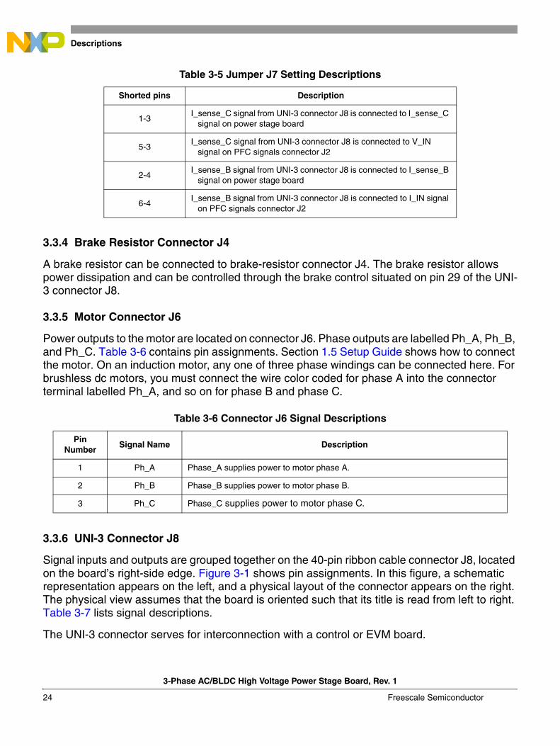
3.3.3 Jumper Terminals J3 and J7
Table 3-4 and Table 3-5 show jumper terminal settings for selected configurations. Each table row means one option of configuration and determines the pins shorted by a jumper plug.
Table 3-4 Jumper J3 Setting Descriptions
Pin Number
Signal Name Description
1 DCB_Pfc_Neg2 Negative bus input and external PFC board negative bus input.
2 DCB_Pfc_Neg1Negative output from input bridge rectifier and external PFC board negative output
from input bridge rectifier.
3 Earth_GND Ground connection for the line input and external PFC board ground.
Pin Number
Signal Name Description
1 DCB_Pfc_Pos2 Positive bus input and external PFC board positive bus input.
2 DCB_Pfc_Pos1Positive output from input bridge rectifier and external PFC board positive output
from input bridge rectifier.
Shorted pins Description
1-3BEMF_sense_C signal from UNI-3 connector J8 is connected to
BEMF_sense_C signal on power stage board
5-3BEMF_sense_C signal from UNI-3 connector J8 is connected to V_IN
signal on PFC signals connector J2
2-4BEMF_sense_B signal from UNI-3 connector J8 is connected to
BEMF_sense_B signal on power stage board
6-4BEMF_sense_B signal from UNI-3 connector J8 is connected to V_IN
signal on PFC signals connector J2
3-Phase AC/BLDC High Voltage Power Stage Board, Rev. 1
Freescale Semiconductor 23‘
Signal Descriptions
3.3.4 Brake Resistor Connector J4
A brake resistor can be connected to brake-resistor connector J4. The brake resistor allows power dissipation and can be controlled through the brake control situated on pin 29 of the UNI-3 connector J8.
3.3.5 Motor Connector J6
Power outputs to the motor are located on connector J6. Phase outputs are labelled Ph_A, Ph_B, and Ph_C. Table 3-6 contains pin assignments. Section 1.5 Setup Guide shows how to connect the motor. On an induction motor, any one of three phase windings can be connected here. For brushless dc motors, you must connect the wire color coded for phase A into the connector terminal labelled Ph_A, and so on for phase B and phase C.
3.3.6 UNI-3 Connector J8
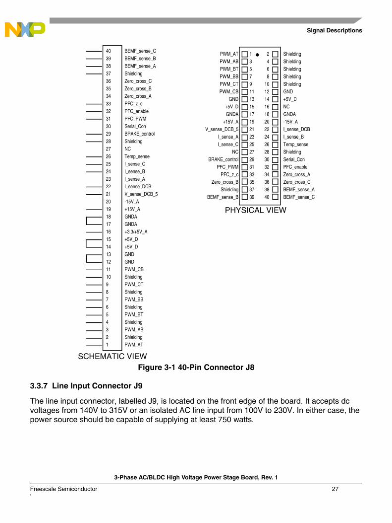
Signal inputs and outputs are grouped together on the 40-pin ribbon cable connector J8, located on the board’s right-side edge. Figure 3-1 shows pin assignments. In this figure, a schematic representation appears on the left, and a physical layout of the connector appears on the right. The physical view assumes that the board is oriented such that its title is read from left to right. Table 3-7 lists signal descriptions.
The UNI-3 connector serves for interconnection with a control or EVM board.
Table 3-5 Jumper J7 Setting Descriptions
Shorted pins Description
1-3I_sense_C signal from UNI-3 connector J8 is connected to I_sense_C
signal on power stage board
5-3I_sense_C signal from UNI-3 connector J8 is connected to V_IN
signal on PFC signals connector J2
2-4I_sense_B signal from UNI-3 connector J8 is connected to I_sense_B
signal on power stage board
6-4I_sense_B signal from UNI-3 connector J8 is connected to I_IN signal
on PFC signals connector J2
Table 3-6 Connector J6 Signal Descriptions
Pin Number
Signal Name Description
1 Ph_A Phase_A supplies power to motor phase A.
2 Ph_B Phase_B supplies power to motor phase B.
3 Ph_C Phase_C supplies power to motor phase C.
3-Phase AC/BLDC High Voltage Power Stage Board, Rev. 1
24 Freescale Semiconductor
Signal Descriptions
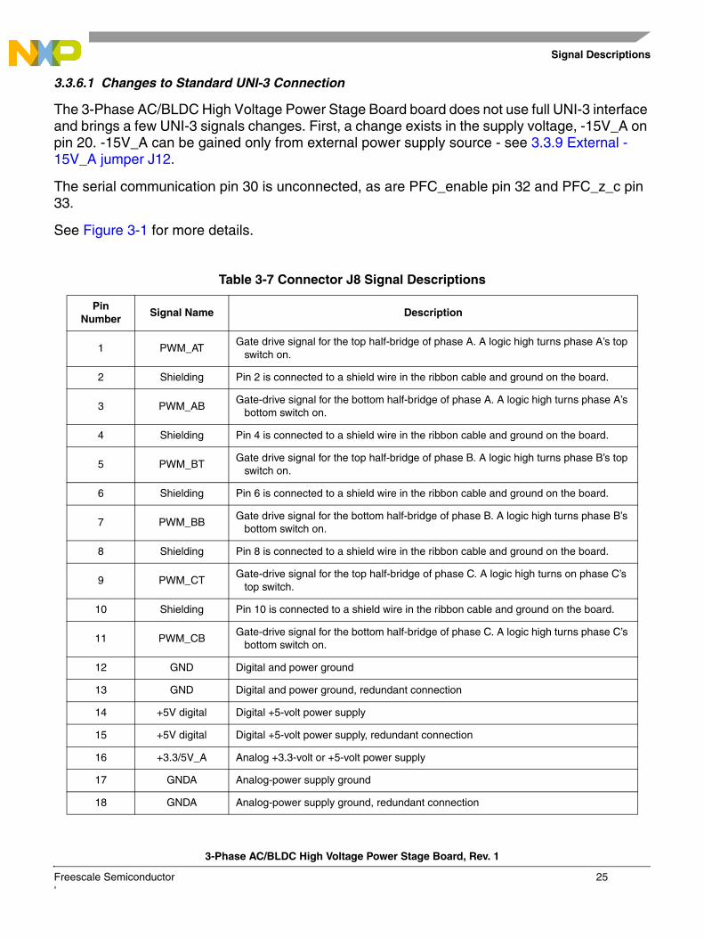
3.3.6.1 Changes to Standard UNI-3 Connection
The 3-Phase AC/BLDC High Voltage Power Stage Board board does not use full UNI-3 interface and brings a few UNI-3 signals changes. First, a change exists in the supply voltage, -15V_A on pin 20. -15V_A can be gained only from external power supply source - see 3.3.9 External -15V_A jumper J12.
The serial communication pin 30 is unconnected, as are PFC_enable pin 32 and PFC_z_c pin 33.
See Figure 3-1 for more details.
Table 3-7 Connector J8 Signal Descriptions
Pin Number
Signal Name Description
1 PWM_ATGate drive signal for the top half-bridge of phase A. A logic high turns phase A’s top
switch on.
2 Shielding Pin 2 is connected to a shield wire in the ribbon cable and ground on the board.
3 PWM_ABGate-drive signal for the bottom half-bridge of phase A. A logic high turns phase A’s
bottom switch on.
4 Shielding Pin 4 is connected to a shield wire in the ribbon cable and ground on the board.
5 PWM_BTGate drive signal for the top half-bridge of phase B. A logic high turns phase B’s top
switch on.
6 Shielding Pin 6 is connected to a shield wire in the ribbon cable and ground on the board.
7 PWM_BBGate drive signal for the bottom half-bridge of phase B. A logic high turns phase B’s
bottom switch on.
8 Shielding Pin 8 is connected to a shield wire in the ribbon cable and ground on the board.
9 PWM_CTGate-drive signal for the top half-bridge of phase C. A logic high turns on phase C’s
top switch.
10 Shielding Pin 10 is connected to a shield wire in the ribbon cable and ground on the board.
11 PWM_CBGate-drive signal for the bottom half-bridge of phase C. A logic high turns phase C’s
bottom switch on.
12 GND Digital and power ground
13 GND Digital and power ground, redundant connection
14 +5V digital Digital +5-volt power supply
15 +5V digital Digital +5-volt power supply, redundant connection
16 +3.3/5V_A Analog +3.3-volt or +5-volt power supply
17 GNDA Analog-power supply ground
18 GNDA Analog-power supply ground, redundant connection
3-Phase AC/BLDC High Voltage Power Stage Board, Rev. 1
Freescale Semiconductor 25‘
Signal Descriptions
19 +15V_A Analog +15-volt power supply
20 -15V_A Analog -15-volt power supply
21 V_sense_DCBAnalog-sense signal that measures bus voltage. It is scaled at 8.09V per volt of dc
bus voltage.
22 I_sense_DCBAnalog-sense signal that measures bus current. It is scaled at 8.09V per amp of dc
bus current.
23 I_sense_AAnalog-sense signal that measures current in phase A. It is scaled at 50V per amp of
dc bus current.
24 I_sense_BAnalog-sense that measures current in phase B. It is scaled at 0.563V per amp of dc
bus current.
25 I_sense_CAnalog-sense signal that measures current in phase C. It is scaled at 0.563 volts per
amp of dc bus current.
26 Temp_sense Analogu-sense signal that measures temperature on the heatsink.
27 NC No connection
28 Shielding Pin 28 is connected to a shield wire in the ribbon cable and ground on the board.
29 Brake_control Gate-drive signal for the brake IGBT.
30 Serial_Con No connection
31 PFC_PWM Digital signal that controls the power factor correction circuit’s switch.
32 PFC_enable No connection
33 PFC_z_c No connection
34 Zero_cross_A Digital signal used for sensing phase A back-EMF zero-crossing events.
35 Zero_cross_B Digital signal used for sensing phase B back-EMF zero-crossing events.
36 Zero_cross_C Digital signal used for sensing phase C back-EMF zero-crossing events.
37 Shielding Pin 37 is connected to a shield wire in the ribbon cable and ground on the board.
38 BEMF_sense_AAnalog-sense signal that measures phase A back EMF. It is scaled at 8.09mV per
volt of dc bus voltage.
39 BEMF_sense_BAnalog-sense signal that measures phase B back EMF. It is scaled at 8.09mV per
volt of dc bus voltage.
40 BEMF_sense_CAnalog-sense signal that measures phase C back EMF. It is scaled at 8.09mV per
volt of dc bus voltage.
Table 3-7 Connector J8 Signal Descriptions (Continued)
Pin Number
Signal Name Description
3-Phase AC/BLDC High Voltage Power Stage Board, Rev. 1
26 Freescale Semiconductor
Signal Descriptions
Figure 3-1 40-Pin Connector J8
3.3.7 Line Input Connector J9
The line input connector, labelled J9, is located on the front edge of the board. It accepts dc voltages from 140V to 315V or an isolated AC line input from 100V to 230V. In either case, the power source should be capable of supplying at least 750 watts.
40393837363534333231302928272625242322212019181716151413121110987654321
BEMF_sense_CBEMF_sense_BBEMF_sense_AShieldingZero_cross_CZero_cross_BZero_cross_APFC_z_cPFC_enablePFC_PWMSerial_ConBRAKE_controlShieldingNCTemp_senseI_sense_CI_sense_BI_sense_AI_sense_DCBV_sense_DCB_5-15V_A+15V_AGNDAGNDA+3.3/+5V_A+5V_D+5V_DGNDGNDPWM_CBShieldingPWM_CTShieldingPWM_BBShieldingPWM_BTShieldingPWM_ABShieldingPWM_AT
SCHEMATIC VIEW
2468
10121416182022242628303234363840
13579111315171921232527293133353739
ShieldingShieldingShieldingShieldingShieldingGND+5V_DNCGNDA-15V_AI_sense_DCBI_sense_BTemp_senseShieldingSerial_ConPFC_enableZero_cross_AZero_cross_CBEMF_sense_ABEMF_sense_C
PWM_ATPWM_ABPWM_BTPWM_BBPWM_CTPWM_CB
GND+5V_DGNDA
+15V_AV_sense_DCB_5
I_sense_AI_sense_C
NCBRAKE_control
PFC_PWMPFC_z_c
Zero_cross_BShielding
BEMF_sense_B
PHYSICAL VIEW
3-Phase AC/BLDC High Voltage Power Stage Board, Rev. 1
Freescale Semiconductor 27‘
Signal Descriptions
3.3.8 Earth Ground Terminal J10
One hole is used as earth ground connection J10. The J10 hole is used for mounting and ground connection of the heatsink.
Connect an earth ground to the earth ground terminal on the heat sink. The heat sink has a screw on its front edge that is marked with a ground symbol.
As mentioned in previous chapters, the 3-phase AC/BLDC High-Voltage Power Stage board contains more grounds. These grounds are connected into one point. If necessary, the user can remove ground connection GC400 to disconnect the grounds and perform measurements.
3.3.9 External -15V_A jumper J12
An external -15V power supply source can be connected to the power stage board through jumper J12 to supply boards connected through UNI-3 connector J8 by -15V_A (pin 20).
3-Phase AC/BLDC High Voltage Power Stage Board, Rev. 1
28 Freescale Semiconductor
Chapter 4 Design Consideration
4.1 Contents4.2 Overview . . . . . . . . . . . . . . . . . . . . . . . . . . . . . . . . . . . . . . . . . . . . . . . . . . 294.3 3-Phase Bridge . . . . . . . . . . . . . . . . . . . . . . . . . . . . . . . . . . . . . . . . . . . . . 304.4 Bus Voltage and Current Feedback. . . . . . . . . . . . . . . . . . . . . . . . . . . . . . 324.5 Over-current and Undervoltage Functions. . . . . . . . . . . . . . . . . . . . . . . . . 344.6 Temperature Sensing . . . . . . . . . . . . . . . . . . . . . . . . . . . . . . . . . . . . . . . . 354.7 Back EMF Signals . . . . . . . . . . . . . . . . . . . . . . . . . . . . . . . . . . . . . . . . . . . 354.8 Phase Current Sensing . . . . . . . . . . . . . . . . . . . . . . . . . . . . . . . . . . . . . . . 364.9 Brake . . . . . . . . . . . . . . . . . . . . . . . . . . . . . . . . . . . . . . . . . . . . . . . . . . . . . 374.10 External Power Factor Correction . . . . . . . . . . . . . . . . . . . . . . . . . . . . . . . 384.11 Test Points and LED Indication . . . . . . . . . . . . . . . . . . . . . . . . . . . . . . . . . 384.12 Power Supplies and Voltage Reference . . . . . . . . . . . . . . . . . . . . . . . . . . 42
4.2 Overview
From a systems point of view, the HV AC power stage fits into an architecture designed for software development. In addition to the hardware needed to run a motor, a variety of feedback signals that facilitate control algorithm development are provided. A set of schematics for the 3-phase AC/BLDC High-Voltage Power-Stage appears in the following section.
Circuit descriptions for the HV AC power stage appear in 4.3 3-Phase Bridge through 4.12 Power Supplies and Voltage Reference. One phase leg of the 3-phase bridge is examined in 4.3 3-Phase Bridge. Bus voltage and bus current feedback are discussed in 4.4 Bus Voltage and Current Feedback. Safety functions are highlighted in 4.5 Over-current and Undervoltage Functions. Temperature sensing is discussed in 4.6 Temperature Sensing. Back-EMF signals appear in 4.7 Back EMF Signals. Phase current sensing is discussed in 4.8 Phase Current Sensing. The brake is highlighted in 4.9 Brake. Power-factor correction is discussed in 4.10 External Power Factor Correction. Test Points description and LED description are made in 4.11 Test Points and LED Indication, and finally, all power supplies and Voltage reference are described in 4.12 Power Supplies and Voltage Reference.
3-Phase AC/BLDC High Voltage Power Stage Board, Rev. 1
Freescale Semiconductor 29

3-Phase Bridge
4.3 3-Phase Bridge
The output stage is configured as a 3-phase bridge with IGBT-output transistors. It is simplified considerably by a high-voltage, integrated-gate driver that has an over-current and undervoltage limit feature. Figure 4-1 shows a schematic of one phase. At the input, pull-down resistors R207 and R208 set a logic low in the absence of a signal. Open input pull-down is important because the power transistors must stay off in case of a broken connection or an absence of power on the control board. The drive signal is buffered and inverted by U200A and U200B. This part has a minimum logic 1 input voltage of 1.2V and a maximum logic 0 input voltage of 0.5V, which allows for inputs from 3.3V or 5V logic. An international rectifier, IR2133, supplies gate drive. IR2133 also provides undervoltage lockout and over-current. Undervoltage lockout is 8.2V/8.6V volts, depending on the current threshold. IR2133 has an implemented 250 ns deadtime insertion. Current limiting and undervoltage lockout are discussed further in 4.5 Over-current and Undervoltage Functions. One important design decisions in a motor drive is the selection of gate-drive impedance for the output transistors. In Figure 4-1, resistor R206, diode D203, and the IR2133 nominal 420-mA current sinking capability determine gate-drive impedance for the lower half-bridge transistor. A similar network is used on the upper half-bridge. These networks set turn-on gate drive impedance at approximately 75 Ω and turn-off gate drive to approximately 420 mA. These values produce transition times of approximately 200 ns.
Transition times of this length represent a carefully weighed compromise between power dissipation and noise generation. Generally, transition times longer than 250 ns tend to get power hungry at non-audible PWM rates; transition times under 50 ns create di/dts so large that proper operation is difficult to achieve. The HV AC power stage is designed with switching times at the higher end of this range to minimize noise.
Anti-parallel diode softness is also a primary design consideration. If the anti-parallel diodes in an off-line motor drive are allowed to snap, the resulting di/dts can cause noise management problems difficult to solve. In general, the peak to zero di/dt should be approximately equal to the di/dt applied to turn off the anti-parallel diodes. The SKP10N60 IGBT’s used in this design are targeted at this kind of reverse recovery.
3-Phase AC/BLDC High Voltage Power Stage Board, Rev. 1
30 Freescale Semiconductor
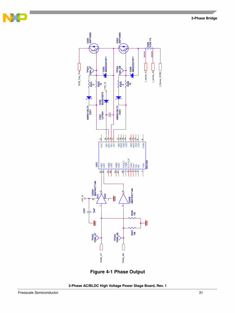
3-Phase Bridge
Figure 4-1 Phase Output
PW
M_A
B
PW
M_A
T
I_S
ense
_DC
B2
I_se
nse_
A1
I_se
nse_
A2
DC
B_C
ap_P
os
GN
D
+15V
_D
GN
D
+5V
_D
GN
D
TP20
4G
ate_
AB
TP20
4G
ate_
AB
TP20
1G
ate_
AT
TP20
1G
ate_
AT
CA
O3
SD
6C
A-
4
VS
S7
FLT-
CLR
2
CA
+5
CO
M8
LO3
9
LO2
10
LO1
11
ITR
IP1
VS
312
LIN
226
LIN
327
FAU
LT28
HO
216
VS
215
VB
314
HIN
223
HO
119
HIN
324
VB
120
HIN
122
VS
118
HO
313
VB
217
VC
C21
LIN
125
U20
1
IR21
33S
U20
1
IR21
33S
12
14 7VC
C
GN
DU20
0AM
M74
HC
T14M
VC
C
GN
DU20
0AM
M74
HC
T14M
D20
5M
MS
Z525
1BT1
D20
5M
MS
Z525
1BT1
D20
3M
BR
S13
0LT3
D20
3M
BR
S13
0LT3
R20
810
kR
208
10k
34
U20
0BM
M74
HC
T14M
U20
0BM
M74
HC
T14M
TP20
2P
WM
_AT
TP20
2P
WM
_AT
D20
1M
BR
S13
0LT3
D20
1M
BR
S13
0LT3
D20
2M
MS
Z525
1BT1
D20
2M
MS
Z525
1BT1
R20
675R20
675
R20
710
kR
207
10k
C20
1
10nF
C20
1
10nF
TP20
3P
WM
_AB
TP20
3P
WM
_AB
C20
21u
F/50
VC
202
1uF/
50V
R20
10
R20
10
R20
40
R20
40
R20
275R20
275
sense
sense
R30
00.
050-
1%
sense
sense
R30
00.
050-
1%
Q30
0S
KP
10N
60Q
300
SK
P10
N60
D20
0M
UR
S16
0T3
D20
0M
UR
S16
0T3
Q30
3S
KP
10N
60Q
303
SK
P10
N60
3-Phase AC/BLDC High Voltage Power Stage Board, Rev. 1
Freescale Semiconductor 31
Bus Voltage and Current Feedback
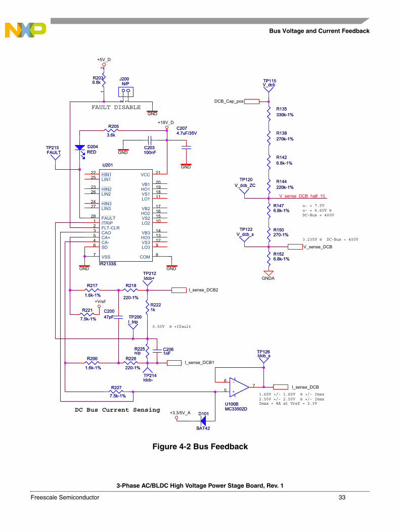
4.4 Bus Voltage and Current Feedback
Figure 4-2 shows the circuitry that provides feedback signals proportional to bus voltage and bus current. Bus voltage is scaled down by a voltage divider consisting of R135, R138, R142, R144, R147, R150, and R152. The values are chosen such that a 400-volt bus voltage corresponds to 3.235V at output V_sense_DCB. An additional output, V_sense_DCB_half_15, provides a reference used in zero-crossing detection. Bus current is sampled by resistor R303 in Figure A-5 and amplified in IR2133’s operational amplifier (Figure 4-2). This circuit provides a voltage output suitable for sampling with A/D (analog-to-digital) inputs. IR2133’s operational amplifier is used as a differential amplifier for bus-current sensing. With R200 = R217, R218 = R226, and R221 = R227, the gain is given by:
A = R227/(R200+R226)
The output voltage is shifted up by +Vref to accommodate positive and negative current swings. A ±400-mV voltage drop across the sense resistor corresponds to a measured current range of ±8 amps. The default current range 8 amps is marked on the actual PCB board (see Figure 4-3). In addition, a -I signal is connected to the ITRIP input of IR2133 and provides an over-current triggering function. A discussion of over-current limiting follows in 4.5 Over-current and Undervoltage Functions.
The output is connected to the UNI-3 pin 22 I_sense_DCB. V_dcb is scaled at 8.09mV per volt of the DC bus voltage and connected to the UNI-3 pin 21 V_sense_DCB_5.
The shunt resistor is represented by a 0.050-ohm resistance Isabellenhutte SMV SMD precision resistor, the same as the phase current measurement resistors.
3-Phase AC/BLDC High Voltage Power Stage Board, Rev. 1
32 Freescale Semiconductor
Bus Voltage and Current Feedback
Figure 4-2 Bus Feedback
V_sense_DCB_half_15
I_sense_DCB2
I_sense_DCB1
V_sense_DCB
DCB_Cap_pos
I_sense_DCB
+18V_D
GND
GND
+5V_D
GND
+Vref
GND
GND
GNDA
+3.3/5V_A
FAULT DISABLE
DC Bus Current Sensing
0.50V @ +Ifault
u- < 7.5Vu- = 6.60V @ DC-Bus = 400V
3.235V @ DC-Bus = 400V
1.65V +/- 1.65V @ +/- Imax2.50V +/- 2.50V @ +/- ImaxImax = 8A at Vref = 3.3V
R138270k-1%R138270k-1%
R227
7.5k-1%
R227
7.5k-1%
D101
BAT42
D101
BAT42
TP122V_dcb_s
TP122V_dcb_s
R1426.8k-1%R1426.8k-1%
R217
1.6k-1%
R217
1.6k-1%
U201
IR2133S
U201
IR2133S
CAO3
SD6 CA-4
VSS7
FLT-CLR2
CA+5
COM 8
LO3 9
LO2 10
LO1 11
ITRIP1
VS3 12
LIN226
LIN327
FAULT28 HO2 16VS2 15
VB3 14
HIN223 HO1 19
HIN324
VB1 20
HIN122
VS1 18
HO3 13
VB2 17
VCC 21LIN125
TP200I_tripTP200I_trip
R2036.8kR2036.8k
12
R135330k-1%R135330k-1%
R226
220-1%
R226
220-1%
C2074.7uF/35VC2074.7uF/35V
TP120V_dcb_ZC
TP120V_dcb_ZC
R144220k-1%R144220k-1%
R150270-1%R150270-1%
R1476.8k-1%R1476.8k-1%
R205
3.6k
R205
3.6k
D204REDD204RED
C203100nFC203100nF
TP215FAULTTP215FAULT
TP126Idcb_sTP126Idcb_s
J200N/P
J200N/P
12
R225n/pR225n/p
R218
220-1%
R218
220-1%
C2061nFC2061nF
TP214Idcb-TP214Idcb-
R2221kR2221k
TP115V_dcbTP115V_dcb
TP212Idcb+TP212Idcb+
R1526.8k-1%R1526.8k-1%
R221
7.5k-1%
R221
7.5k-1%
R200
1.6k-1%
R200
1.6k-1%
C20047pFC20047pF
+
-
U100BMC33502D
+
-
U100BMC33502D
5
67
3-Phase AC/BLDC High Voltage Power Stage Board, Rev. 1
Freescale Semiconductor 33
Over-current and Undervoltage Functions
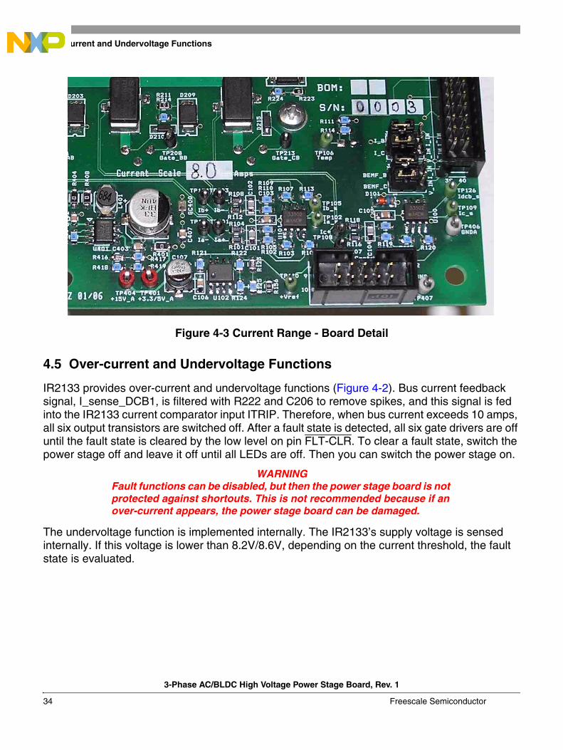
Figure 4-3 Current Range - Board Detail
4.5 Over-current and Undervoltage Functions
IR2133 provides over-current and undervoltage functions (Figure 4-2). Bus current feedback signal, I_sense_DCB1, is filtered with R222 and C206 to remove spikes, and this signal is fed into the IR2133 current comparator input ITRIP. Therefore, when bus current exceeds 10 amps, all six output transistors are switched off. After a fault state is detected, all six gate drivers are off until the fault state is cleared by the low level on pin FLT-CLR. To clear a fault state, switch the power stage off and leave it off until all LEDs are off. Then you can switch the power stage on.
WARNINGFault functions can be disabled, but then the power stage board is not protected against shortouts. This is not recommended because if an over-current appears, the power stage board can be damaged.
The undervoltage function is implemented internally. The IR2133’s supply voltage is sensed internally. If this voltage is lower than 8.2V/8.6V, depending on the current threshold, the fault state is evaluated.
3-Phase AC/BLDC High Voltage Power Stage Board, Rev. 1
34 Freescale Semiconductor
Temperature Sensing
4.6 Temperature Sensing
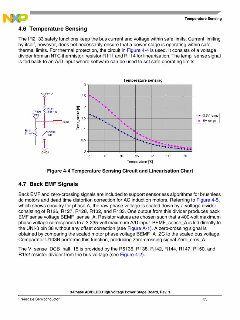
The IR2133 safety functions keep the bus current and voltage within safe limits. Current limiting by itself, however, does not necessarily ensure that a power stage is operating within safe thermal limits. For thermal protection, the circuit in Figure 4-4 is used. It consists of a voltage divider from an NTC thermistor, resistor R111 and R114 for linearisation. The temp_sense signal is fed back to an A/D input where software can be used to set safe operating limits.
Figure 4-4 Temperature Sensing Circuit and Linearisation Chart
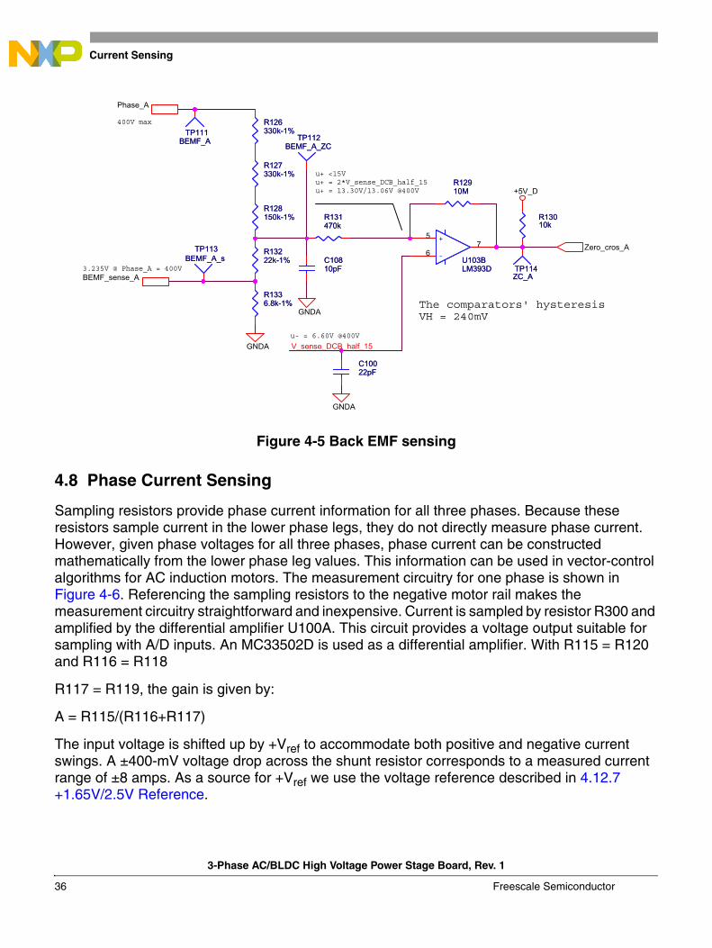
4.7 Back EMF Signals
Back EMF and zero-crossing signals are included to support sensorless algorithms for brushless dc motors and dead time distortion correction for AC induction motors. Referring to Figure 4-5, which shows circuitry for phase A, the raw phase voltage is scaled down by a voltage divider consisting of R126, R127, R128, R132, and R133. One output from this divider produces back EMF sense voltage BEMF_sense_A. Resistor values are chosen such that a 400-volt maximum phase voltage corresponds to a 3.235-volt maximum A/D input. BEMF_sense_A is led directly to the UNI-3 pin 38 without any offset correction (see Figure A-1). A zero-crossing signal is obtained by comparing the scaled motor phase voltage BEMF_A_ZC to the scaled bus voltage. Comparator U103B performs this function, producing zero-crossing signal Zero_cros_A.
The V_sense_DCB_half_15 is provided by the R5135, R138, R142, R144, R147, R150, and R152 resistor divider from the bus voltage (see Figure 4-2).
Temp
GNDA
+3.3/5V_A
12
RV10010kRV10010k
R1145.1k-1%R1145.1k-1%
TP106TempTP106
Temp
R1113.6k-1%R1113.6k-1%
3-Phase AC/BLDC High Voltage Power Stage Board, Rev. 1
Freescale Semiconductor 35
Phase Current Sensing
Figure 4-5 Back EMF sensing
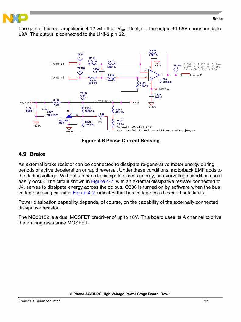
4.8 Phase Current Sensing
Sampling resistors provide phase current information for all three phases. Because these resistors sample current in the lower phase legs, they do not directly measure phase current. However, given phase voltages for all three phases, phase current can be constructed mathematically from the lower phase leg values. This information can be used in vector-control algorithms for AC induction motors. The measurement circuitry for one phase is shown in Figure 4-6. Referencing the sampling resistors to the negative motor rail makes the measurement circuitry straightforward and inexpensive. Current is sampled by resistor R300 and amplified by the differential amplifier U100A. This circuit provides a voltage output suitable for sampling with A/D inputs. An MC33502D is used as a differential amplifier. With R115 = R120 and R116 = R118
R117 = R119, the gain is given by:
A = R115/(R116+R117)
The input voltage is shifted up by +Vref to accommodate both positive and negative current swings. A ±400-mV voltage drop across the shunt resistor corresponds to a measured current range of ±8 amps. As a source for +Vref we use the voltage reference described in 4.12.7 +1.65V/2.5V Reference.
V_sense_DCB_half_15
Phase_A
Zero_cros_A
BEMF_sense_A
GNDA
GNDA
+5V_D
GNDA
The comparators' hysteresisVH = 240mV
u- = 6.60V @400V
400V max
3.235V @ Phase_A = 400V
u+ <15Vu+ = 2*V_sense_DCB_half_15u+ = 13.30V/13.06V @400V
R126330k-1%R126330k-1%
R12910MR12910M
R128150k-1%R128150k-1%
TP114ZC_ATP114ZC_A
R1336.8k-1%R1336.8k-1%
TP112BEMF_A_ZC
TP112BEMF_A_ZC
TP113BEMF_A_s
TP113BEMF_A_s C108
10pFC10810pF
R131470kR131470k
R13222k-1%R13222k-1%
5
67
+
- U103BLM393D
+
- U103BLM393D
R127330k-1%R127330k-1%
TP111BEMF_A
TP111BEMF_A
R13010kR13010k
C10022pFC10022pF
3-Phase AC/BLDC High Voltage Power Stage Board, Rev. 1
36 Freescale Semiconductor
Brake
The gain of this op. amplifier is 4.12 with the +Vref offset, i.e. the output ±1.65V corresponds to ±8A. The output is connected to the UNI-3 pin 22.
Figure 4-6 Phase Current Sensing
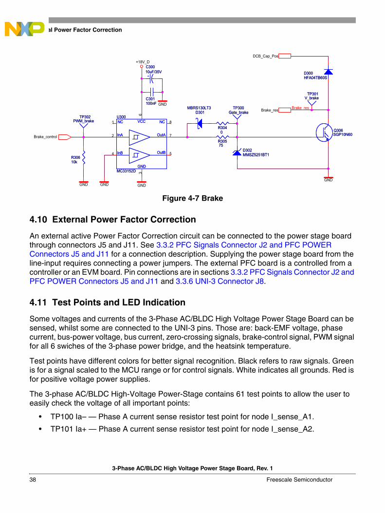
4.9 Brake
An external brake resistor can be connected to dissipate re-generative motor energy during periods of active deceleration or rapid reversal. Under these conditions, motorback EMF adds to the dc bus voltage. Without a means to dissipate excess energy, an overvoltage condition could easily occur. The circuit shown in Figure 4-7, with an external dissipative resistor connected to J4, serves to dissipate energy across the dc bus. Q306 is turned on by software when the bus voltage sensing circuit in Figure 4-2 indicates that bus voltage could exceed safe limits.
Power dissipation capability depends, of course, on the capability of the externally connected dissipative resistor.
The MC33152 is a dual MOSFET predriver of up to 18V. This board uses its A channel to drive the braking resistance MOSFET.
I_sense_CI_sense_C2
I_sense_C1
GNDA
GNDA
+15V_A +Vref
GNDA
+3.3/5V_A
GNDA
1.65V/2.5V ref
Default +Vref=1.65VFor +Vref=2.5V solder R156 or a wire jumper
1.65V +/- 1.65V @ +/- Imax2.50V +/- 2.50V @ +/- ImaxImax = 8A at Vref = 3.3V
N/P
R12347k-1%R12347k-1%
+
C10710uF/20V
+
C10710uF/20V R156
0
R156
0
R118220-1%R118
220-1%
C106100nFC106100nF
TP109Ic_sTP109Ic_s
R116220-1%R116
220-1%
R115
7.5k-1%
R115
7.5k-1%
8
5
4U102LM285MU102LM285M
R117
1.6k-1%
R117
1.6k-1%
R1251k-1%R1251k-1%
R122100k-1%R122100k-1%
R119
1.6k-1%
R119
1.6k-1%3
21
84
+
-
U100AMC33502D
+
-
U100AMC33502D
R121
6.2k
R121
6.2k
C105100nFC105100nF
TP107Ic-
TP107Ic-
C10447pFC10447pF
R1207.5k-1%R1207.5k-1%
TP110+VrefTP110
+Vref
TP108Ic+
TP108Ic+
R12433k-1%R12433k-1%
3-Phase AC/BLDC High Voltage Power Stage Board, Rev. 1
Freescale Semiconductor 37
External Power Factor Correction
Figure 4-7 Brake
4.10 External Power Factor Correction
An external active Power Factor Correction circuit can be connected to the power stage board through connectors J5 and J11. See 3.3.2 PFC Signals Connector J2 and PFC POWER Connectors J5 and J11 for a connection description. Supplying the power stage board from the line-input requires connecting a power jumpers. The external PFC board is a controlled from a controller or an EVM board. Pin connections are in sections 3.3.2 PFC Signals Connector J2 and PFC POWER Connectors J5 and J11 and 3.3.6 UNI-3 Connector J8.
4.11 Test Points and LED Indication
Some voltages and currents of the 3-Phase AC/BLDC High Voltage Power Stage Board can be sensed, whilst some are connected to the UNI-3 pins. Those are: back-EMF voltage, phase current, bus-power voltage, bus current, zero-crossing signals, brake-control signal, PWM signal for all 6 swiches of the 3-phase power bridge, and the heatsink temperature.
Test points have different colors for better signal recognition. Black refers to raw signals. Green is for a signal scaled to the MCU range or for control signals. White indicates all grounds. Red is for positive voltage power supplies.
The 3-phase AC/BLDC High-Voltage Power-Stage contains 61 test points to allow the user to easily check the voltage of all important points:
• TP100 Ia– — Phase A current sense resistor test point for node I_sense_A1.
• TP101 Ia+ — Phase A current sense resistor test point for node I_sense_A2.
Brake_res
Brake_control
DCB_Cap_Pos
Brake_resGND
GNDGND GND
+18V_D
GND
R3040R3040
TP300Gate_brakeTP300
Gate_brake
+
C30010uF/35V
+
C30010uF/35V
R30575R30575
D300HFA04TB60SD300HFA04TB60S
D302MMSZ5251BT1D302MMSZ5251BT1
Q306SGP10N60Q306SGP10N60
TP301V_brakeTP301V_brake
TP302PWM_brake
TP302PWM_brake
D301MBRS130LT3
D301MBRS130LT3
C301100nFC301100nF
R30610kR30610k
OutBInB
GND
InA
NC NC
OutA
VCCU300
MC33152D
OutBInB
GND
InA
NC NC
OutA
VCCU300
MC33152D
23
5
67
81
4
3-Phase AC/BLDC High Voltage Power Stage Board, Rev. 1
38 Freescale Semiconductor
Test Points and LED Indication
• TP102 Ia_s — Phase A current output test point for node I_sense_A, scaled at 0.275V/0.417V per amp of phase current A and shifted by 1.65V/2.5V.
• TP103 Ib– — Phase B current sense resistor test point for node I_sense_B1.
• TP104 Ib+ — Phase B current sense resistor test point for node I_sense_B2.
• TP105 Ib_s — Phase B current output test point of node I_sense_B, scaled at 0.275/0.417 volts per amp of phase current B and shifted by 1.65V/2.5V.
• TP106 Temp — Temperature sensing testing point.
• TP107 Ic– — Phase C current sense resistor test point for node I_sense_C1.
• TP108 Ic+ — Phase C current sense resistor test point for node I_sense_C2.
• TP109 Ic_s — Phase C current output test point of node I_sense_C, scaled at 0.275/0.417 volts per amp of phase current C and shifted by 1.65V/2.5V.
• TP106 Temp — Temperature sensing test point.
• TP110 +Vref — Reference voltage test point.
• TP111 BEMF_A — Back EMF phase A test point.
• TP112 BEMF_A_ZC — Phase A zero-crossing test point, scaled at 33.25V per volt of phase voltage A.
• TP113 BEMF_A_s — Back EMF phase A test point, scaled at 8.09V per volt of phase voltage A.
• TP114 ZC_A — Phase A zero-crossing test point.
• TP115 V_dcb — Bus voltage test point.
• TP116 BEMF_B — Back EMF phase B test point.
• TP117 BEMF_B_ZC — Phase B zero-crossing test point, scaled at 33.25V per volt of phase voltage B.
• TP118 BEMF_B_s — Back EMF phase B test point, scaled at 8.09V per volt of phase voltage B.
• TP119 ZC_B — Phase B zero-crossing test point.
• TP120 V_dcb_ZC — Half of bus voltage test point used for zero-crossing comparison.
• TP121 BEMF_C — Back EMF phase C test point.
• TP122 V_dcb_s — Bus voltage test point, scaled at 8.09V per volt.
• TP123 BEMF_C_ZC — Phase C zero-crossing test point, scaled at 33.25V per volt of phase voltage C.
• TP124 ZC_C — Phase C zero-crossing test point.
• TP125 BEMF_C_s — Back EMF phase C test point, scaled at 8.09V per volt of phase voltage C.
• TP126 Idcb_s — Bus current scaled and shifted +1.65V/+2.5V.
3-Phase AC/BLDC High Voltage Power Stage Board, Rev. 1
Freescale Semiconductor 39

Test Points and LED Indication
• TP200 I_trip — Over-current and under-voltage shut-down test point of 3-phase bridge driver U201.
• TP201 Gate_AT TP200 I_trip —Top transistor gate of phase A test point.
• TP202 PWM_AT — PWM control signal for top transistor gate of phase A, test point on connector J8 pin.
• TP203 PWM_AB — PWM control signal for bottom transistor gate of phase A, test point on connector J8 pin.
• TP204 Gate_AB — Bottom transistor gate of phase A test point.
• TP205 Gate_BT — Top transistor gate of phase B test point.
• TP206 PWM_BT — PWM control signal for top transistor gate of phase B, test point on connector J8 pin.
• TP207 PWM_BB — PWM control signal for bottom transistor gate of phase B, test point on connector J8 pin.
• TP208 Gate_BB — Bottom transistor gate of phase B test point.
• TP209 PWM_CT — PWM control signal for top transistor gate of phase C, test point on connector J8 pin.
• TP210 Gate_CT — Top transistor gate of phase C test point.
• TP211 PWM_CB — PWM control signal for bottom transistor gate of phase C, test point on connector J8 pin.
• TP212 Idcb+ — Bus current sense resistor test point for node I_sense_DCB2.
• TP213 Gate_CB — Bottom transistor gate of phase C test point.
• TP214 Idcb– — Bus current sense resistor test point for node I_sense_DCB1.
• TP215 FAULT — Over-current or undervoltage of the 3-phase bridge driver IR2133 test point.
• TP300 Gate_brake — Brake transistor gate test point.
• TP301 V_brake — Brake resistor voltage test point.
• TP302 PWM_brake — PWM control signal for brake transistor gate, test point on connector J8 pin 29 Brake Control.
• TP303 AC1 — Main input voltage test point on connector J9 pin 1.
• TP304 AC2 — Main input voltage test point on connector J9 pin 2.
• TP400 GNDA — Analog ground test point.
• TP401 +3.3V/5V_A — This point is the output of the U401 linear voltage regulator. It serves as the power supply for the on-board op. amplifiers and for supplying the temperature measuring circuit. It is connected to the PFC signals connector J2.
• TP402 +18V — This point is an output of the U402 switching step-up/down inverter. It serves as the power supply for U401, U404 and +18V_D digital supplies.
3-Phase AC/BLDC High Voltage Power Stage Board, Rev. 1
40 Freescale Semiconductor
Test Points and LED Indication
• TP403 +18V_D — This point is an output of the U402 switching step-up/down inverter. It serves as the power supply for the comparators, for the MOSFET driver and the 3-phase bridge driver, and as the source for U403 in generating +5V_D. It is connected to the PFC signals connector J2.
• TP404 +15V_A — This point is an output of the U404 linear voltage regulator. It serves as the power supply for the voltage reference source. It is connected to the UNI-3 connector J8 pin 19.
• TP405 +12VFAN — This point is the output of the U400 step-up/down inverter. It serves as a power supply for the fans only.
• TP406 GNDA — Analog ground test point.
• TP407 GND — Ground test point.
• TP408 GND — Ground test point.
• TP409 GND — Ground test point.
• TP410 GND — Ground test point.
• TP411 +5V_D — This point is the output of the U403 switching step-down inverter. It serves as the power supply for the on-board logic IC’s. It is connected to the UNI-3 connector J8 pins 14 and 15 and to the PFC signals connector J2.
• TP412 V_dcb_1 — Bus voltage test point.
• TP413 V_dcb_2 — Bus voltage test point.
This board also contains four LEDs as indicators:
• D204 — Indicates over-current or undervoltage of the 3-phase bridge driver IR2133 (see Figure 4-2).
• D400 — Indicates that the +12V_Fans level is properly generated.
• D403 — Indicates that the +18V level is properly generated.
• D407 — Indicates that the +5V_D level is properly generated.
For more details see Figure 4-8.
Figure 4-8 LED Indication
+5V_D+12V_FANS
GNDGNDGND
TP402+18VTP402+18V
D407GREEND407GREEN
D403GREEND403GREEN
R4132.7kR4132.7k
R400820R400820
D400GREEND400GREEN
R4073.6kR4073.6k
3-Phase AC/BLDC High Voltage Power Stage Board, Rev. 1
Freescale Semiconductor 41
Power Supplies and Voltage Reference
4.12 Power Supplies and Voltage Reference
The 3-phase AC/BLDC High-Voltage Power-Stage contains devices that require various voltage levels of +18V, +15V, +12V and +5V or +3.3V.
4.12.1 Input Power Supply
All power supplies are served from bus voltage. Bus can be supplied from two sources, from the line input across the power bridge or from the external PFC board. The power source should be able to deliver at least 8 amps.
Figure 4-9 DC Bus Power Supply
4.12.2 +18V Power Supply
The +18V level is generated by means of the LNK306P switching step-up/down inverter (see Figure 4-10) that generates this level from bus voltage. This inverter can supply up to 300 mA. This voltage level serves the LM317LD and MC78L15ACD linear regulators, comparators, 3-phase bridge driver and brake gate driver. +18V_D is directly supplied from LNK306P. If the LNK306P inverter operates properly, the D403 green LED is lit.
Earth_GND
AC1
AC2
DCB_Cap_Pos
DCB_Cap_Neg
DCB_Pfc_Pos2DCB_Pfc_Pos1
DCB_Pfc_Neg1 DCB_Pfc_Neg2
F300
Fuse
F300
Fuse
TP304AC2TP304AC2
+
C304470uF/400V
+
C304470uF/400V
C30310nF/3000V
C30310nF/3000V
D304V14E250
D304V14E250
C30210nF/3000V
C30210nF/3000V
i
R307
SG-200
i
R307
SG-200
+
C305470uF/400V
+
C305470uF/400V
TP303AC1
TP303AC1
-+
D303GBU605
-+
D303GBU605
2
1
3
4
3-Phase AC/BLDC High Voltage Power Stage Board, Rev. 1
42 Freescale Semiconductor
Power Supplies and Voltage Reference
Figure 4-10 +18V Power Supply
4.12.3 +15V_A Power Supply
The +15V_A power supply is generated from the +18V level by means of the MC78L15ACD linear voltage regulator (see Figure 4-11). It can supply up to 100 mA. The +15V_A level is used to supply the linear voltage reference LM285M. It is connected to the UNI-3 connector J8 pin 19.
Figure 4-11 +15V_A Power Supply
4.12.4 +5V_D Power Supply
An important voltage level for this board is +5V_D. This voltage level is obtained by the LM2674M switching step-down inverter and can supply up to 500 mA (Figure 4-12). The +5V_D level is used to supply the on-board logic IC’s. It is connected to the PFC signals connector J2 and to the UNI-3 connector J8 pins 14 and 15.
DCB_Cap_Pos
GND
+18V_D
TP402+18VTP402+18V
+ C4064.7uF/400V
+ C4064.7uF/400V
12
R406
0
R406
0
U402
LNK306P
U402
LNK306P
S 1S 2
BP3FB4
D5
S 7S 8
R402
18.7k
R402
18.7k
D403GREEND403GREEN
R4032kR4032k
C404100nFC404100nF
R405
0
R405
0
D402BYV26CD402BYV26C
L400
1mH
L400
1mH
TP403+18V_DTP403
+18V_D
+
C401
N/P
+
C401
N/P
12
+ C40510uF/35V
+ C40510uF/35V
12
TP412V_dcb_1TP412
V_dcb_1
R4073.6kR4073.6k
D4011N4005D4011N4005
+ C400150uF/20V
+ C400150uF/20V
12
GNDA
+15V_A
GNDAGNDA
R408
0
R408
0
U404MC78L15ACDU404MC78L15ACD
VI8 VO 1
GND1
2GND2
3GND3
6GND4
7
C407100nFC407100nF
TP402+18VTP402+18V TP404
+15V_ATP404+15V_A
+ C4081uF/50V
+ C4081uF/50V
12
3-Phase AC/BLDC High Voltage Power Stage Board, Rev. 1
Freescale Semiconductor 43
Power Supplies and Voltage Reference
Figure 4-12 +5V_D Power Supply
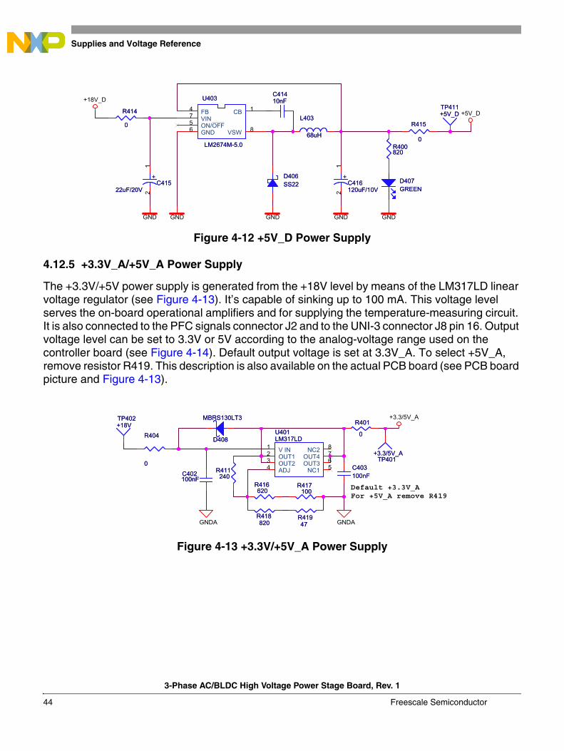
4.12.5 +3.3V_A/+5V_A Power Supply
The +3.3V/+5V power supply is generated from the +18V level by means of the LM317LD linear voltage regulator (see Figure 4-13). It’s capable of sinking up to 100 mA. This voltage level serves the on-board operational amplifiers and for supplying the temperature-measuring circuit. It is also connected to the PFC signals connector J2 and to the UNI-3 connector J8 pin 16. Output voltage level can be set to 3.3V or 5V according to the analog-voltage range used on the controller board (see Figure 4-14). Default output voltage is set at 3.3V_A. To select +5V_A, remove resistor R419. This description is also available on the actual PCB board (see PCB board picture and Figure 4-13).
Figure 4-13 +3.3V/+5V_A Power Supply
GNDGNDGNDGND
+5V_D
GND
+18V_D
R415
0
R415
0
C41410nFC41410nF
L403
68uH
L403
68uH
D407GREEND407GREEN
+C415
22uF/20V
+C415
22uF/20V
12
TP411+5V_DTP411+5V_D
R400820R400820
D406SS22D406SS22
U403
LM2674M-5.0
U403
LM2674M-5.0
CB 1FB4
ON/OFF5 VIN7
VSW 8GND6
R414
0
R414
0
+C416120uF/10V
+C416120uF/10V
12
+3.3/5V_A
GNDA GNDA
Default +3.3V_AFor +5V_A remove R419
R404
0
R404
0
R418820
R418820
D408
MBRS130LT3
D408
MBRS130LT3TP402+18VTP402+18V
C402100nFC402100nF
R411240
R411240
U401LM317LDU401LM317LD
V IN1OUT12OUT23ADJ4 NC1 5OUT3 6OUT4 7NC2 8
R401
0
R401
0
R41947
R41947
C403100nFC403100nF
R416620
R416620
R417100
R417100
TP401+3.3/5V_A
TP401+3.3/5V_A
3-Phase AC/BLDC High Voltage Power Stage Board, Rev. 1
44 Freescale Semiconductor
Power Supplies and Voltage Reference
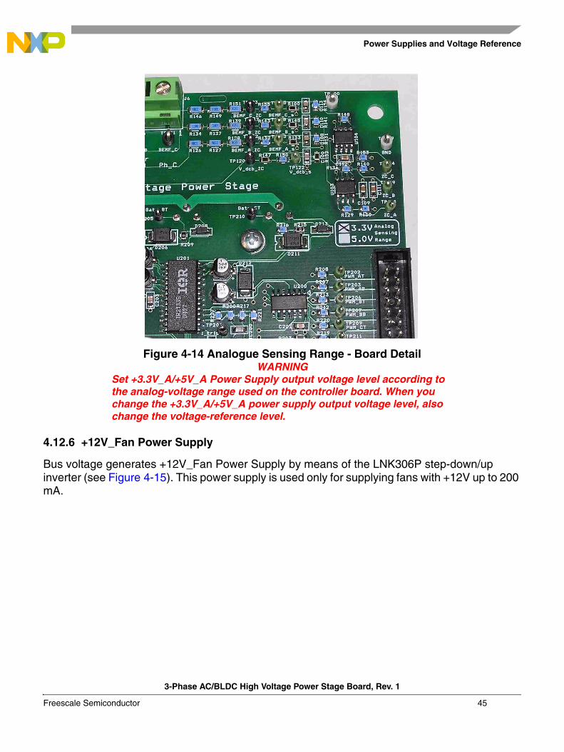
Figure 4-14 Analogue Sensing Range - Board DetailWARNING
Set +3.3V_A/+5V_A Power Supply output voltage level according to the analog-voltage range used on the controller board. When you change the +3.3V_A/+5V_A power supply output voltage level, also change the voltage-reference level.
4.12.6 +12V_Fan Power Supply
Bus voltage generates +12V_Fan Power Supply by means of the LNK306P step-down/up inverter (see Figure 4-15). This power supply is used only for supplying fans with +12V up to 200 mA.
3-Phase AC/BLDC High Voltage Power Stage Board, Rev. 1
Freescale Semiconductor 45
Power Supplies and Voltage Reference
Figure 4-15 +12V_Fan Power Supply
4.12.7 +1.65V/2.5V Reference
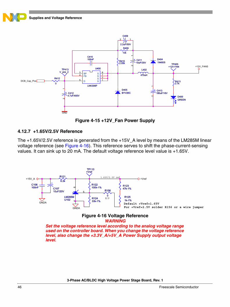
The +1.65V/2.5V reference is generated from the +15V_A level by means of the LM285M linear voltage reference (see Figure 4-16). This reference serves to shift the phase-current-sensing values. It can sink up to 20 mA. The default voltage reference level value is +1.65V.
Figure 4-16 Voltage ReferenceWARNING
Set the voltage reference level according to the analog voltage range used on the controller board. When you change the voltage reference level, also change the +3.3V_A/+5V_A Power Supply output voltage level.
DCB_Cap_Pos
GND
+12V_FANS1
2
+ C4124.7uF/400V
+ C4124.7uF/400V
12 +
C409
2.2uF/50V
+
C409
2.2uF/50V
S 1S 2
BP3FB4
D5
S 7S 8
U400
LNK306P
U400
LNK306P
TP413V_dcb_2
TP413V_dcb_2
R409
13k
R409
13k
D400GREEND400GREEN
R412
0
R412
0
12
+ C413180uF/16V
+ C413180uF/16V
R4132.7kR4132.7k
C410100nFC410100nF
D405BYV26CD405BYV26C
TP405+12V FAN
TP405+12V FAN
L402
470uH
L402
470uH
R4102.05kR4102.05k
12
+ C41110uF/35V
+ C41110uF/35V
D4041N4005D4041N4005
GNDA
GNDA
+15V_A +Vref1.65V/2.5V ref
Default +Vref=1.65VFor +Vref=2.5V solder R156 or a wire jumper
N/P
R156
0
R156
0
R12347k-1%R12347k-1%
R121
6.2k
R121
6.2kR122100k-1%R122100k-1%
C106100nFC106100nF
TP110+VrefTP110
+Vref
8
5
4U102LM285MU102LM285M
+
C10710uF/20V
+
C10710uF/20V
R12433k-1%R12433k-1%
R1251k-1%R1251k-1%
3-Phase AC/BLDC High Voltage Power Stage Board, Rev. 1
46 Freescale Semiconductor
Appendix A. 3-Phase AC/BLDC High Voltage Power Stage Board Schematics
3-Phase AC/BLDC High Voltage Power Stage Board, Rev. 1
Freescale Semiconductor 47
48F
reescale Sem
iconductor
GND
GNDA
+3.3/5V_A
+5V_D+3.3/5V_A
GNDA
+15V_A
GND
+18V_D+5V_D+Vref
Sheilding
Sheilding
Sheilding
Sheilding
Sheilding
Sheilding
Sheilding
Serial_Con
BEMF_sense_ABEMF_sense_BBEMF_sense_C
Zero_cross_AZero_cross_BZero_cross_C
PWM_AT
PWM_AB
PWM_BT
PWM_BB
PWM_CT
PWM_CB
PFC_z_cPFC_enablePFC_PWM
Brake_control
Temp_senseI_sense_CI_sense_BI_sense_AI_sense_DCBV_sense_DCB
PWM_PFCGNDV_INI_IN
GNDA
External-15V_A
+5V_A
+5V_D+Vref
GND+18V_D
PFC signals
UNI-3
J8
CON/40
J8
CON/40
12345678910111213141516171819202122232425262728293031323334353637383940
J2
CON/10
J2
CON/10
10
7654321
98
J12J12
12
J7
JUMPERS_2_CH
J7
JUMPERS_2_CH
1
53
2
64
J3
JUMPERS_2_CH
J3
JUMPERS_2_CH
1
53
2
64
3-Ph
ase AC
/BL
DC
Hig
h Vo
ltage P
ower S
tage B
oard
, Rev. 1
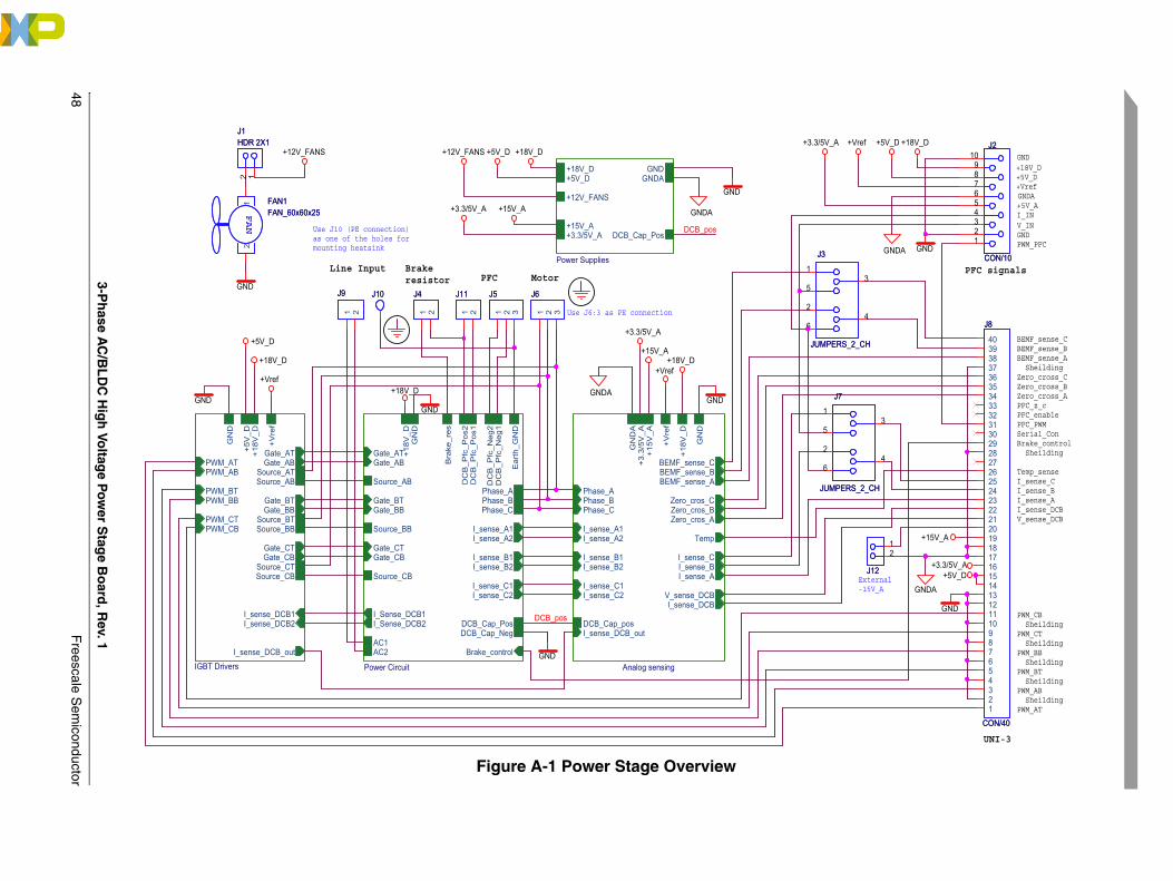
Figure A-1 Power Stage Overview
DCB_pos
DCB_pos
+18V_D+5V_D+12V_FANS
+18V_D
GND
+15V_A+3.3/5V_A GNDA
+Vref+Vref
+18V_D+15V_A
GND
+5V_D
+12V_FANS
+3.3/5V_A
GNDAGND
+18V_D
GND
GND
GND
Use J10 (PE connection)as one of the holes formounting heatsink
Brakeresistor
Line InputPFC Motor
Use J6:3 as PE connection
Analog sensing
I_sense_BI_sense_A
I_sense_CI_sense_B2I_sense_B1
I_sense_C2I_sense_C1
I_sense_A1I_sense_A2 Temp
+V
ref
+15
V_A
+3.
3/5V
_AG
ND
A
BEMF_sense_C
Phase_A
Phase_C
GN
D
+18
V_D
Zero_cros_BZero_cros_A
Phase_B
BEMF_sense_B
Zero_cros_C
BEMF_sense_A
V_sense_DCB
DCB_Cap_posI_sense_DCB_out
I_sense_DCB
J9J9
1 2
J1HDR 2X1J1HDR 2X1
12
IGBT Drivers
+18
V_D
+5V
_D
GN
D
PWM_BTPWM_BB
PWM_CTPWM_CB
PWM_ABPWM_AT
Gate_ATGate_AB
Source_ABSource_AT
Gate_BTGate_BB
Source_BBSource_BT
Gate_CTGate_CB
Source_CBSource_CT
+V
ref
I_sense_DCB2I_sense_DCB1
I_sense_DCB_out
J5J5
1 2 3
Power Supplies
+18V_D
+15V_A
+12V_FANS
+5V_D GNDAGND
DCB_Cap_Pos+3.3/5V_A
J4J4
1 2
J11J11
1 2
FAN
FAN1FAN_60x60x25F
AN
FAN1FAN_60x60x25
12
J10J10
Power Circuit
Gate_AT
Phase_A
Gate_AB
I_sense_A1I_sense_A2
Gate_BT Phase_BGate_BB
I_sense_B1I_sense_B2
Gate_CT
Phase_C
Gate_CB
I_sense_C1I_sense_C2
I_Sense_DCB1I_Sense_DCB2
Brake_control
DCB_Cap_PosDCB_Cap_Neg
Bra
ke_r
es
GN
D+
18V
_D
Ear
th_G
ND
AC1AC2
DC
B_P
fc_P
os2
DC
B_P
fc_P
os1
Source_AB
Source_BB
Source_CB
DC
B_P
fc_N
eg1
DC
B_P
fc_N
eg2
J6J6
1 2 3
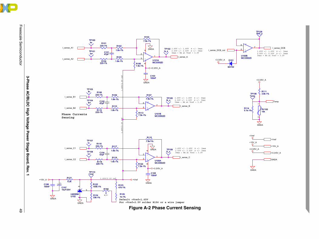
Freescale S
emiconductor
49
Temp
+Vref
+15V_A
+3.3/5V_A
GNDA
CB_outI_sense_DCB
GNDA
+3.3/5V_A
GNDA
+Vref
+15V_A
+3.3/5V_A
.3/5V_A
1.65V +/- 1.65V @ +/- Imax2.50V +/- 2.50V @ +/- ImaxImax = 8A at Vref = 3.3V
5
67
+
-
U100BMC33502D
+
-
U100BMC33502D
D101
BAT42
D101
BAT42
12
RV10010kRV10010k
R1145.1k-1%R1145.1k-1%
TP106TempTP106
Temp
R1113.6k-1%R1113.6k-1%
TP126Idcb_sTP126Idcb_s
3-Ph
ase AC
/BL
DC
Hig
h Vo
ltage P
ower S
tage B
oard
, Rev. 1
Figure A-2 Phase Current Sensing
I_sense_B
I_sense_A
I_sense_C
I_sense_B2
I_sense_B1
I_sense_C2
I_sense_C1
I_sense_A1
I_sense_A2
I_sense_D
GNDA
GNDA
+15V_A +Vref
GNDA
+3.3/5V_A
GNDA
GNDA
GNDA
+3.3/5V_A
+3
1.65V/2.5V ref
Default +Vref=1.65VFor +Vref=2.5V solder R156 or a wire jumper
1.65V/2.5V ref
1.65V/2.5V ref
Phase CurrentsSensing
1.65V +/- 1.65V @ +/- Imax2.50V +/- 2.50V @ +/- ImaxImax = 8A at Vref = 3.3V
1.65V +/- 1.65V @ +/- Imax2.50V +/- 2.50V @ +/- ImaxImax = 8A at Vref = 3.3V
1.65V +/- 1.65V @ +/- Imax2.50V +/- 2.50V @ +/- ImaxImax = 8A at Vref = 3.3V
N/P
TP105Ib_sTP105Ib_s
TP101Ia+
TP101Ia+
R103
7.5k-1%
R103
7.5k-1%
R109
1.6k-1%
R109
1.6k-1%
R101220-1%
R101220-1%
R12347k-1%R12347k-1%
R102
1.6k-1%
R102
1.6k-1%
+
C10710uF/20V
+
C10710uF/20V
TP100Ia-
TP100Ia-
R110
1.6k-1%
R110
1.6k-1%
R156
0
R156
0
R118220-1%R118
220-1%
R107
7.5k-1%
R107
7.5k-1%
C106100nFC106100nF
TP109Ic_sTP109Ic_s
C10247pFC10247pF
R116220-1%R116
220-1%
R115
7.5k-1%
R115
7.5k-1%
8
5
4U102LM285MU102LM285M
R104220-1%
R104220-1%
TP104Ib+
TP104Ib+
TP103Ib-
TP103Ib-
R117
1.6k-1%
R117
1.6k-1%
R1251k-1%R1251k-1%
R122100k-1%R122100k-1%
R1067.5k-1%R1067.5k-1%
TP102Ia_sTP102Ia_s
5
67
+
-
U101BMC33502D
+
-
U101BMC33502D
R119
1.6k-1%
R119
1.6k-1%
R1137.5k-1%R1137.5k-1%
R112220-1%
R112220-1%
3
21
84
+
-
U101AMC33502D
+
-
U101AMC33502D
3
21
84
+
-
U100AMC33502D
+
-
U100AMC33502D
R121
6.2k
R121
6.2k
C105100nFC105100nF
TP107Ic-
TP107Ic-
C10147pFC10147pF
C10447pFC10447pF
R1207.5k-1%R1207.5k-1%
TP110+VrefTP110
+Vref
R108220-1%
R108220-1%
TP108Ic+
TP108Ic+
C103100nFC103100nF
R12433k-1%R12433k-1%
R105
1.6k-1%
R105
1.6k-1%
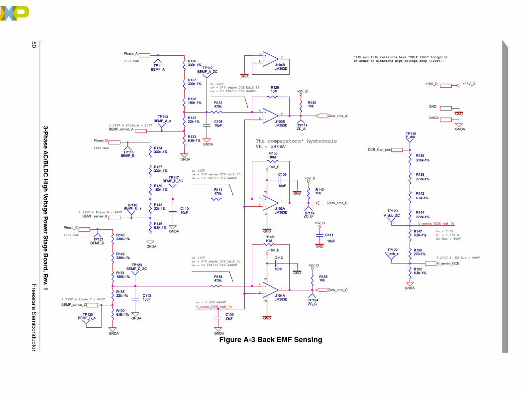
50F
reescale Sem
iconductor
V_sense_DCB_half_15
GND
GNDA
+18V_D
V_sense_DCB
DCB_Cap_pos
GNDA
GND
+18V_D
GNDA
0k and 150k resistors have "SM/R_1206" footprint order to withstand high voltage drop (<200V).
u- < 7.5Vu- = 6.60V @ DC-Bus = 400V
3.235V @ DC-Bus = 400V
R144220k-1%R144220k-1%
R150270-1%R150270-1%
R1476.8k-1%R1476.8k-1%
TP115V_dcbTP115V_dcb
TP120V_dcb_ZC
TP120V_dcb_ZC
R1526.8k-1%R1526.8k-1%
R138270k-1%R138270k-1%
TP122V_dcb_s
TP122V_dcb_s
R1426.8k-1%R1426.8k-1%
R135330k-1%R135330k-1%
3-Ph
ase AC
/BL
DC
Hig
h Vo
ltage P
ower S
tage B
oard
, Rev. 1
Figure A-3 Back EMF Sensing
V_sense_DCB_half_15BEMF_sense_C
Phase_A
Phase_C
Zero_cros_B
Zero_cros_A
Phase_B
BEMF_sense_B
Zero_cros_C
BEMF_sense_A
GND
GND
+5V_D
GNDA
GNDA
GNDA
GNDA
GNDA
GNDA
+5V_D
+5V_D
GND
GNDA
GND
+5V_D
+18V_D
GND
+18V_D
GND
33in
3.235V @ Phase_B = 400V
The comparators' hysteresisVH = 240mV
u- = 6.60V @400V
400V max
400V max
400V max
3.235V @ Phase_C = 400V
3.235V @ Phase_A = 400V
u+ <15Vu+ = 2*V_sense_DCB_half_15u+ = 13.30V/13.06V @400V
u+ <15Vu+ = 2*V_sense_DCB_half_15u+ = 13.30V/13.06V @400V
u+ <15Vu+ = 2*V_sense_DCB_half_15u+ = 13.30V/13.06V @400V
R139150k-1%R139150k-1%
R14810MR14810M
TP125BEMF_C_s
TP125BEMF_C_s
C109
10nF
C109
10nFR14010kR14010k
R137330k-1%R137330k-1%
TP124ZC_CTP124ZC_C
C111
10nF
C111
10nF
C10810pFC10810pF
TP117BEMF_B_ZC
TP117BEMF_B_ZC
R13610MR13610M
TP114ZC_ATP114ZC_A
R1006.8k-1%R1006.8k-1%
+
- U104BLM393D
+
- U104BLM393D
5
67
+
- U103BLM393D
+
- U103BLM393D
5
67
R15522k-1%R15522k-1%
R134330k-1%R134330k-1%
C112
10nF
C112
10nF
TP121BEMF_C
TP121BEMF_C
TP113BEMF_A_s
TP113BEMF_A_s
R154470kR154470k
R141470kR141470k
TP118BEMF_B_s
TP118BEMF_B_s
R131470kR131470k
+
- U103ALM393D
+
- U103ALM393D
3
21
84
TP111BEMF_A
TP111BEMF_A
R1456.8k-1%R1456.8k-1%
TP123BEMF_C_ZC
TP123BEMF_C_ZC
C10022pFC10022pF
R14322k-1%R14322k-1%
C11310pFC11310pF
C11010pFC11010pF
R13010kR13010k
TP112BEMF_A_ZC
TP112BEMF_A_ZC
R13222k-1%R13222k-1%
R15310kR15310k
R1336.8k-1%R1336.8k-1%
+
- U104ALM393D
+
- U104ALM393D
3
21
84
R149330k-1%R149330k-1%
R128150k-1%R128150k-1%
R151150k-1%R151150k-1%
R126330k-1%R126330k-1%
TP116BEMF_B
TP116BEMF_B
R146330k-1%R146330k-1%
R12910MR12910M
R127330k-1%R127330k-1%
TP119ZC_BTP119ZC_B
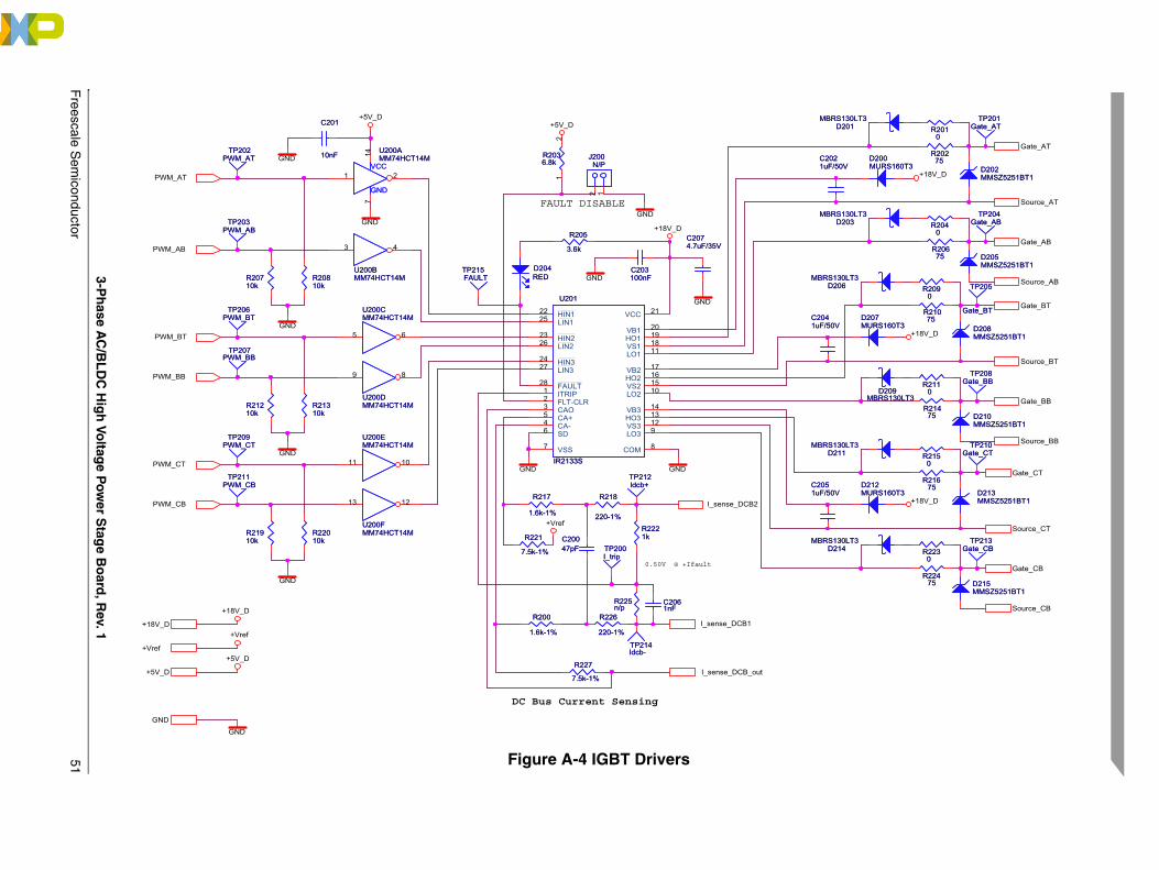
Freescale S
emiconductor
51
Gate_AT
Gate_AB
Source_AB
Source_AT
Gate_BT
Gate_BB
Source_BB
Source_BT
Gate_CT
Gate_CB
Source_CB
Source_CT
+18V_D
+18V_D
+18V_D
TP204Gate_AB
TP204Gate_AB
R21475
R21475
D213MMSZ5251BT1D213MMSZ5251BT1
TP205
Gate_BT
TP205
Gate_BT
TP208Gate_BB
TP208Gate_BB
C2041uF/50VC2041uF/50V
R22475
R22475
TP201Gate_AT
TP201Gate_AT
R21075
R21075
C2051uF/50VC2051uF/50V
R2090
R2090
D205MMSZ5251BT1D205MMSZ5251BT1
R2110
R2110
R21675
R21675
D211MBRS130LT3
D211MBRS130LT3 TP210
Gate_CTTP210
Gate_CT
D214MBRS130LT3
D214MBRS130LT3
D207MURS160T3D207MURS160T3
D203MBRS130LT3
D203MBRS130LT3
D212MURS160T3D212MURS160T3
TP213Gate_CB
TP213Gate_CB
D201MBRS130LT3
D201MBRS130LT3
D209MBRS130LT3
D209MBRS130LT3
D206MBRS130LT3
D206MBRS130LT3
D202MMSZ5251BT1D202MMSZ5251BT1
R20675
R20675
C2021uF/50VC2021uF/50V
R2150
R2150
R2230
R2230
R20275
R20275
R2040
R2040
D210MMSZ5251BT1D210MMSZ5251BT1
R2010
R2010
D215MMSZ5251BT1D215MMSZ5251BT1
D200MURS160T3D200MURS160T3
D208MMSZ5251BT1D208MMSZ5251BT1
3-Ph
ase AC
/BL
DC
Hig
h Vo
ltage P
ower S
tage B
oard
, Rev. 1
Figure A-4 IGBT Drivers
+18V_D
+5V_D
GND
PWM_BT
PWM_BB
PWM_CT
PWM_CB
PWM_AB
PWM_AT
+Vref
I_sense_DCB2
I_sense_DCB1
I_sense_DCB_out
+18V_D
+5V_D
GND
GND
GND
GND
GND
+5V_D
GND
+18V_D
GND
GND
+5V_D
GND
+Vref
+Vref
GND
GND
FAULT DISABLE
DC Bus Current Sensing
0.50V @ +Ifault
R227
7.5k-1%
R227
7.5k-1%
TP200I_tripTP200I_trip
U201
IR2133S
U201
IR2133S
CAO3
SD6 CA-4
VSS7
FLT-CLR2
CA+5
COM 8
LO3 9
LO2 10
LO1 11
ITRIP1
VS3 12
LIN226
LIN327
FAULT28 HO2 16VS2 15
VB3 14
HIN223 HO1 19
HIN324
VB1 20
HIN122
VS1 18
HO3 13
VB2 17
VCC 21LIN125
R217
1.6k-1%
R217
1.6k-1%
C2074.7uF/35VC2074.7uF/35V
VCC
GND
U200AMM74HCT14M
VCC
GND
U200AMM74HCT14M
1 2
147
R226
220-1%
R226
220-1%
R2036.8kR2036.8k
12
TP206PWM_BT
TP206PWM_BT
TP209PWM_CT
TP209PWM_CT
U200DMM74HCT14MU200DMM74HCT14M
9 8
R20810kR20810k
U200BMM74HCT14MU200BMM74HCT14M
3 4
U200FMM74HCT14MU200FMM74HCT14M
13 12
TP202PWM_AT
TP202PWM_AT
R205
3.6k
R205
3.6k
TP215FAULTTP215FAULT
R21910kR21910k
C203100nFC203100nF
D204REDD204RED
J200N/P
J200N/P
12
R21210kR21210k
U200CMM74HCT14MU200CMM74HCT14M
5 6
TP207PWM_BB
TP207PWM_BB
R20710kR20710k
R218
220-1%
R218
220-1%
R225n/pR225n/p
R2221kR2221k
TP214Idcb-TP214Idcb-
TP203PWM_AB
TP203PWM_AB
C201
10nF
C201
10nF
TP211PWM_CB
TP211PWM_CB
C2061nFC2061nF
U200EMM74HCT14MU200EMM74HCT14M
11 10
R22010kR22010k
R21310kR21310k
TP212Idcb+TP212Idcb+
C20047pFC20047pF
R200
1.6k-1%
R200
1.6k-1%
R221
7.5k-1%
R221
7.5k-1%
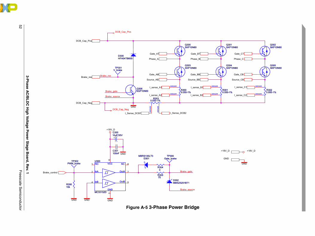
52F
reescale Sem
iconductor
Gate_CT
Phase_C
Gate_CB
I_sense_C1
I_sense_C2
GND
+18V_D
Source_CB
GND
+18V_D
Q301SKP10N60Q301SKP10N60
se
se
R3010.050-1%
se
se
R3010.050-1%
Q302SKP10N60Q302SKP10N60
Q305SKP10N60Q305SKP10N60
Q304SKP10N60Q304SKP10N60
sense
sense
R3020.050-1%
sense
sense
R3020.050-1%
3-Ph
ase AC
/BL
DC
Hig
h Vo
ltage P
ower S
tage B
oard
, Rev. 1
Figure A-5 3-Phase Power Bridge
Brake_gate
Brake_gate
Brake_source
Brake_res
Brake_source
Gate_AT
Phase_A
Gate_AB
I_sense_A1
I_sense_A2
Gate_BT
Phase_B
Gate_BB
I_sense_B1
I_sense_B2
I_Sense_DCB1 I_Sense_DCB2
Brake_control
DCB_Cap_Pos
DCB_Cap_Neg
Brake_resSource_AB Source_BB
GND
GNDGND GND
+18V_D
GND
DCB_Cap_Pos
DCB_Cap_Neg
R3040
R3040
TP300Gate_brake
TP300Gate_brake
sen
sen
sen
sen
+
C30010uF/35V
+
C30010uF/35V
R30575R30575
sense
sense
R3030.050-1%
sense
sense
R3030.050-1%
D300HFA04TB60SD300HFA04TB60S
D302MMSZ5251BT1D302MMSZ5251BT1
sense
sense
R3000.050-1%
sense
sense
R3000.050-1%
Q306SGP10N60Q306SGP10N60
TP301V_brake
TP301V_brake
TP302PWM_brake
TP302PWM_brake
Q300SKP10N60Q300SKP10N60
D301MBRS130LT3
D301MBRS130LT3
C301100nFC301100nF
Q303SKP10N60Q303SKP10N60
R30610kR30610k
OutBInB
GND
InA
NC NC
OutA
VCCU300
MC33152D
OutBInB
GND
InA
NC NC
OutA
VCCU300
MC33152D
2
3
5
6
7
81
4
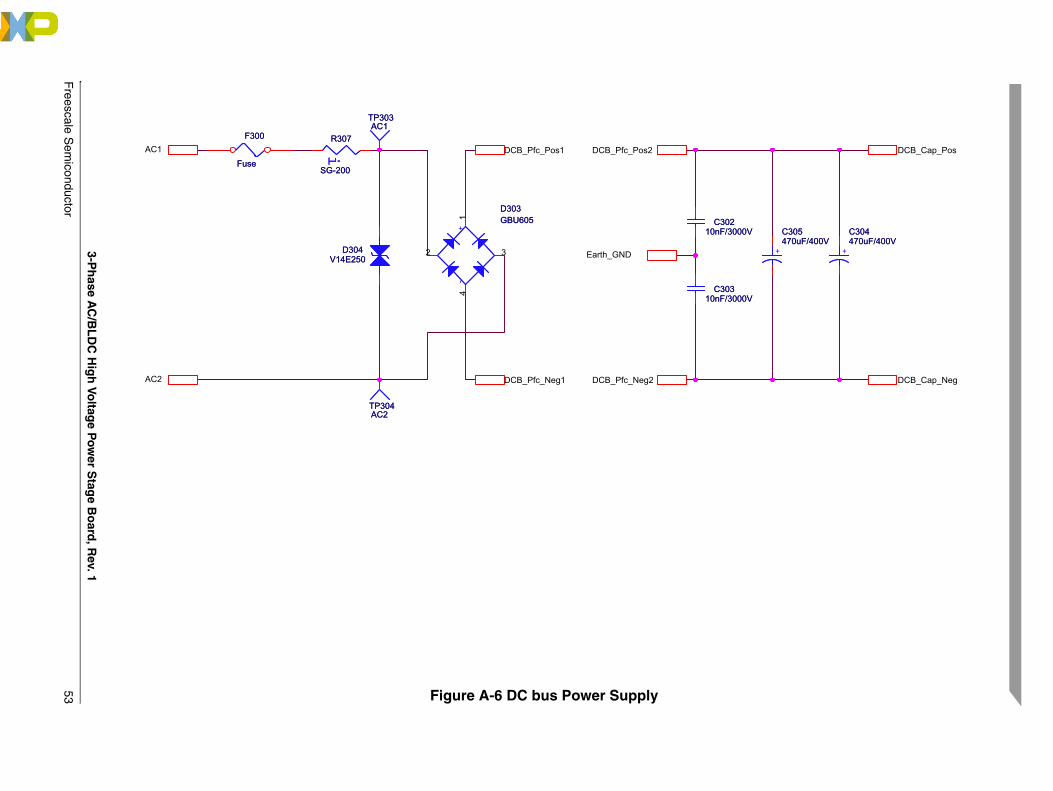
Freescale S
emiconductor
53
DCB_Cap_Pos
DCB_Cap_Neg
+
C304470uF/400V
+
C304470uF/400V
303F/3000V303F/3000V
302F/3000V302F/3000V
+
C305470uF/400V
+
C305470uF/400V
3-Phase A
C/B
LD
C H
igh
Voltag
e Pow
er Stag
e Bo
ard, R
ev. 1
Figure A-6 DC bus Power Supply
Earth_GND
AC1
AC2
DCB_Pfc_Pos2DCB_Pfc_Pos1
DCB_Pfc_Neg1 DCB_Pfc_Neg2
F300
Fuse
F300
Fuse
TP304AC2TP304AC2
C10n
C10n
D304V14E250
D304V14E250
C10n
C10n
i
R307
SG-200
i
R307
SG-200
TP303AC1
TP303AC1
-+
D303GBU605
-+
D303GBU605
2
1
3
4
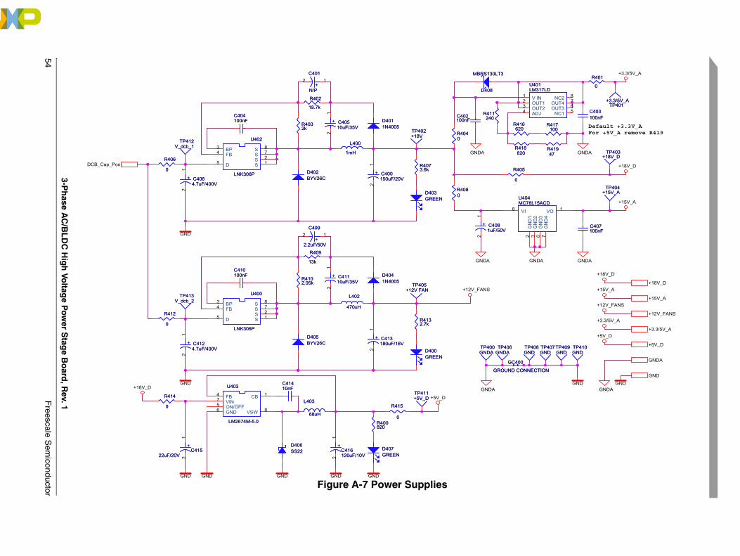
54F
reescale Sem
iconductor
+18V_D
+15V_A
+12V_FANS
+5V_D
GNDA
GND
+3.3/5V_A
+18V_D
+18V_D
+15V_A
+12V_FANS
+5V_D
GND
+15V_A
GNDAGND
GNDA
+3.3/5V_A
GNDA
+3.3/5V_A
GNDA
Default +3.3V_AFor +5V_A remove R419
TP410GNDTP410GND
U404MC78L15ACDU404MC78L15ACD
VI8 VO 1
GN
D1
2G
ND
23
GN
D3
6G
ND
47
R418820
R418820 TP403
+18V_DTP403
+18V_D
406A
406A
TP409GNDTP409GND
C407100nFC407100nF
TP404+15V_A
TP404+15V_A
TP408GNDTP408GND
GC400
UND CONNECTION
GC400
UND CONNECTION
U401LM317LDU401LM317LD
V IN1OUT12OUT23ADJ4 NC1 5OUT3 6OUT4 7NC2 8
R41947
R41947
R401
0
R401
0
R405
0
R405
0
C403100nFC403100nF
TP401+3.3/5V_A
TP401+3.3/5V_A
R417100
R417100
R416620
R416620
TP407GNDTP407GND
3-Ph
ase AC
/BL
DC
Hig
h Vo
ltage P
ower S
tage B
oard
, Rev. 1
Figure A-7 Power Supplies
DCB_Cap_Pos
GNDGNDGNDGND
+5V_D
GND
+12V_FANS
GND
GND
+18V_D
GNDA
GNDA
GNDA
C41410nFC41410nF
R4032kR4032k
R4080R4080
U400
LNK306P
U400
LNK306P
S 1S 2
BP3FB4
D5
S 7S 8
R402
18.7k
R402
18.7k
+
C409
2.2uF/50V
+
C409
2.2uF/50V
12
L400
1mH
L400
1mH
+ C4124.7uF/400V
+ C4124.7uF/400V
12
C404100nFC404100nF
TP413V_dcb_2
TP413V_dcb_2
R4040R4040
TP411+5V_DTP411+5V_D
R409
13k
R409
13k
+
C401
N/P
+
C401
N/P
12
+ C40510uF/35V
+ C40510uF/35V
12
D407GREEND407GREEN
+C415
22uF/20V
+C415
22uF/20V
12
D400GREEND400GREEN
+ C413180uF/16V
+ C413180uF/16V
12
R412
0
R412
0
+C416120uF/10V
+C416120uF/10V
12
C410100nFC410100nF
TPGNDTP
GND
R4132.7kR4132.7k
D408
MBRS130LT3
D408
MBRS130LT3
TP412V_dcb_1
TP412V_dcb_1
R415
0
R415
0
TP402+18VTP402+18V
TP405+12V FAN
TP405+12V FAN
R400820R400820
D405BYV26CD405BYV26C
L402
470uH
L402
470uH
R411240
R411240
GROGRO
R414
0
R414
0
D4011N4005D4011N4005
C402100nFC402100nF
R406
0
R406
0
R4102.05kR4102.05k
+ C4064.7uF/400V
+ C4064.7uF/400V
12
+ C41110uF/35V
+ C41110uF/35V
12
TP400GNDATP400GNDA
+ C400150uF/20V
+ C400150uF/20V
12
D403GREEND403GREEN
L403
68uH
L403
68uH
D406SS22D406SS22
D402BYV26CD402BYV26C
R4073.6kR4073.6k
U403
LM2674M-5.0
U403
LM2674M-5.0
CB 1FB4
ON/OFF5 VIN7
VSW 8GND6
U402
LNK306P
U402
LNK306P
S 1S 2
BP3FB4
D5
S 7S 8
D4041N4005D4041N4005
+ C4081uF/50V
+ C4081uF/50V
12
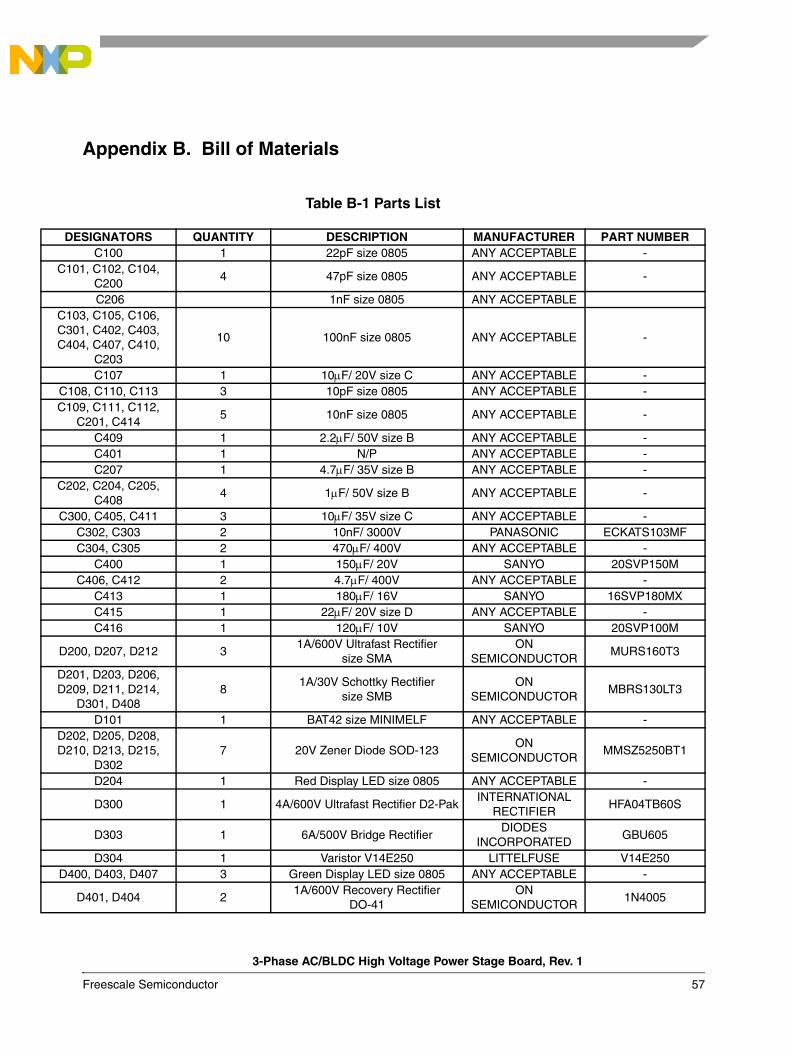
D
C1
C1C3C4
C1C1
C2
C3
D2
D2D2
D2D2
D4
Appendix B. Bill of Materials
Table B-1 Parts List
ESIGNATORS QUANTITY DESCRIPTION MANUFACTURER PART NUMBERC100 1 22pF size 0805 ANY ACCEPTABLE -
01, C102, C104, C200
4 47pF size 0805 ANY ACCEPTABLE -
C206 1nF size 0805 ANY ACCEPTABLE03, C105, C106, 01, C402, C403, 04, C407, C410,
C203
10 100nF size 0805 ANY ACCEPTABLE -
C107 1 10μF/ 20V size C ANY ACCEPTABLE -08, C110, C113 3 10pF size 0805 ANY ACCEPTABLE -09, C111, C112, C201, C414
5 10nF size 0805 ANY ACCEPTABLE -
C409 1 2.2μF/ 50V size B ANY ACCEPTABLE -C401 1 N/P ANY ACCEPTABLE -C207 1 4.7μF/ 35V size B ANY ACCEPTABLE -
02, C204, C205, C408
4 1μF/ 50V size B ANY ACCEPTABLE -
00, C405, C411 3 10μF/ 35V size C ANY ACCEPTABLE -C302, C303 2 10nF/ 3000V PANASONIC ECKATS103MFC304, C305 2 470μF/ 400V ANY ACCEPTABLE -
C400 1 150μF/ 20V SANYO 20SVP150MC406, C412 2 4.7μF/ 400V ANY ACCEPTABLE -
C413 1 180μF/ 16V SANYO 16SVP180MXC415 1 22μF/ 20V size D ANY ACCEPTABLE -C416 1 120μF/ 10V SANYO 20SVP100M
00, D207, D212 31A/600V Ultrafast Rectifier
size SMAON
SEMICONDUCTORMURS160T3
01, D203, D206, 09, D211, D214, D301, D408
81A/30V Schottky Rectifier
size SMBON
SEMICONDUCTORMBRS130LT3
D101 1 BAT42 size MINIMELF ANY ACCEPTABLE -02, D205, D208, 10, D213, D215,
D3027 20V Zener Diode SOD-123
ON SEMICONDUCTOR
MMSZ5250BT1
D204 1 Red Display LED size 0805 ANY ACCEPTABLE -
D300 1 4A/600V Ultrafast Rectifier D2-PakINTERNATIONAL
RECTIFIERHFA04TB60S
D303 1 6A/500V Bridge RectifierDIODES
INCORPORATEDGBU605
D304 1 Varistor V14E250 LITTELFUSE V14E25000, D403, D407 3 Green Display LED size 0805 ANY ACCEPTABLE -
D401, D404 21A/600V Recovery Rectifier
DO-41ON
SEMICONDUCTOR1N4005
3-Phase AC/BLDC High Voltage Power Stage Board, Rev. 1
Freescale Semiconductor 57
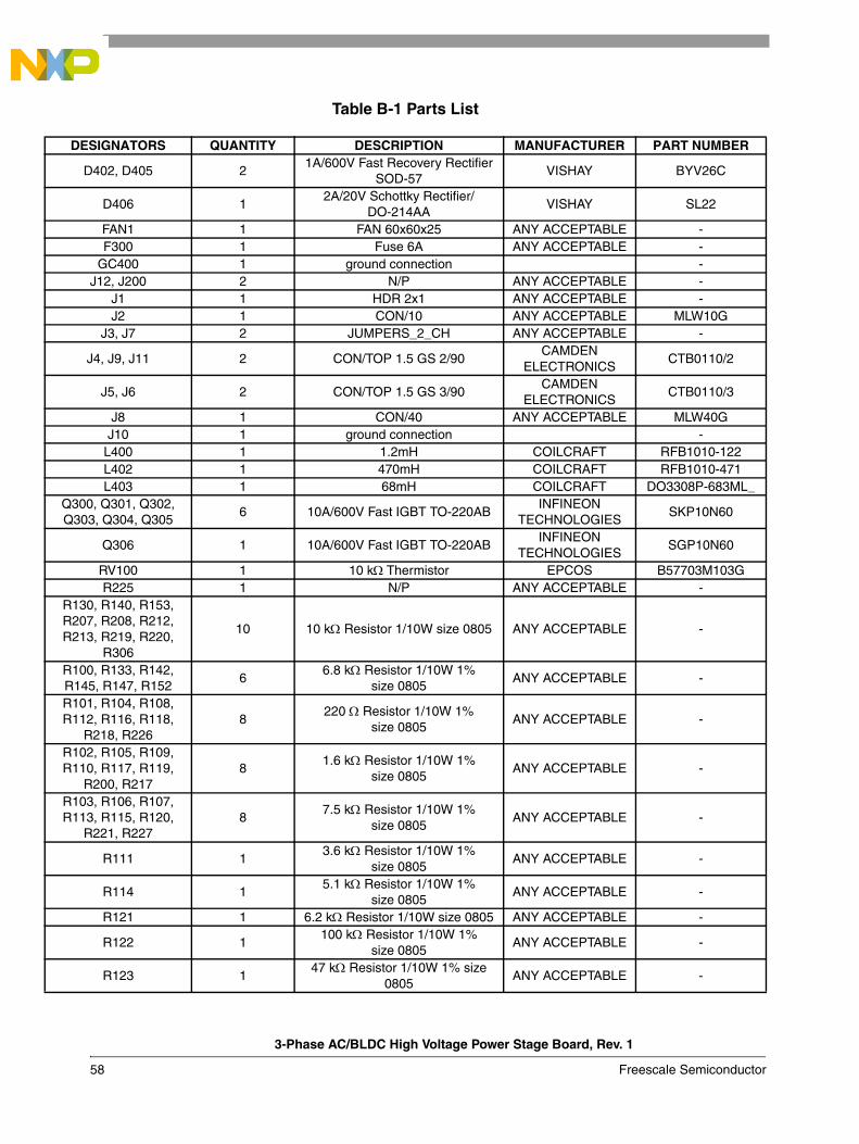
Q3Q3
R1R2R2
R1R1R1R1
R1R1
R1R1
D
D402, D405 21A/600V Fast Recovery Rectifier
SOD-57VISHAY BYV26C
D406 12A/20V Schottky Rectifier/
DO-214AAVISHAY SL22
FAN1 1 FAN 60x60x25 ANY ACCEPTABLE -F300 1 Fuse 6A ANY ACCEPTABLE -
GC400 1 ground connection -J12, J200 2 N/P ANY ACCEPTABLE -
J1 1 HDR 2x1 ANY ACCEPTABLE -J2 1 CON/10 ANY ACCEPTABLE MLW10G
J3, J7 2 JUMPERS_2_CH ANY ACCEPTABLE -
J4, J9, J11 2 CON/TOP 1.5 GS 2/90CAMDEN
ELECTRONICSCTB0110/2
J5, J6 2 CON/TOP 1.5 GS 3/90CAMDEN
ELECTRONICSCTB0110/3
J8 1 CON/40 ANY ACCEPTABLE MLW40GJ10 1 ground connection -
L400 1 1.2mH COILCRAFT RFB1010-122L402 1 470mH COILCRAFT RFB1010-471L403 1 68mH COILCRAFT DO3308P-683ML_
00, Q301, Q302, 03, Q304, Q305
6 10A/600V Fast IGBT TO-220ABINFINEON
TECHNOLOGIESSKP10N60
Q306 1 10A/600V Fast IGBT TO-220ABINFINEON
TECHNOLOGIESSGP10N60
RV100 1 10 kΩ Thermistor EPCOS B57703M103GR225 1 N/P ANY ACCEPTABLE -
30, R140, R153, 07, R208, R212, 13, R219, R220,
R306
10 10 kΩ Resistor 1/10W size 0805 ANY ACCEPTABLE -
00, R133, R142, 45, R147, R152
66.8 kΩ Resistor 1/10W 1%
size 0805ANY ACCEPTABLE -
01, R104, R108, 12, R116, R118, R218, R226
8220 Ω Resistor 1/10W 1%
size 0805ANY ACCEPTABLE -
02, R105, R109, 10, R117, R119, R200, R217
81.6 kΩ Resistor 1/10W 1%
size 0805ANY ACCEPTABLE -
03, R106, R107, 13, R115, R120, R221, R227
87.5 kΩ Resistor 1/10W 1%
size 0805ANY ACCEPTABLE -
R111 13.6 kΩ Resistor 1/10W 1%
size 0805ANY ACCEPTABLE -
R114 15.1 kΩ Resistor 1/10W 1%
size 0805ANY ACCEPTABLE -
R121 1 6.2 kΩ Resistor 1/10W size 0805 ANY ACCEPTABLE -
R122 1100 kΩ Resistor 1/10W 1%
size 0805ANY ACCEPTABLE -
R123 147 kΩ Resistor 1/10W 1% size
0805ANY ACCEPTABLE -
Table B-1 Parts List
ESIGNATORS QUANTITY DESCRIPTION MANUFACTURER PART NUMBER
3-Phase AC/BLDC High Voltage Power Stage Board, Rev. 1
58 Freescale Semiconductor
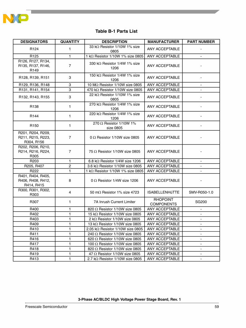
R1R1
R1
R1R1
R1
R2R2
R2R2
R4R4
R3
D
R124 133 kΩ Resistor 1/10W 1% size
0805ANY ACCEPTABLE -
R125 1 1 kΩ Resistor 1/10W 1% size 0805 ANY ACCEPTABLE -26, R127, R134, 35, R137, R146,
R1497
330 kΩ Resistor 1/4W 1% size 1206
ANY ACCEPTABLE -
28, R139, R151 3150 kΩ Resistor 1/4W 1% size
1206ANY ACCEPTABLE -
29, R136, R148 3 10 MΩ Resistor 1/10W size 0805 ANY ACCEPTABLE -31, R141, R154 3 470 kΩ Resistor 1/10W size 0805 ANY ACCEPTABLE -
32, R143, R155 322 kΩ Resistor 1/10W 1% size
0805ANY ACCEPTABLE -
R138 1270 kΩ Resistor 1/4W 1% size
1206ANY ACCEPTABLE -
R144 1220 kΩ Resistor 1/4W 1% size
1206ANY ACCEPTABLE -
R150 1270 Ω Resistor 1/10W 1%
size 0805ANY ACCEPTABLE -
01, R204, R209, 11, R215, R223, R304, R156
7 0 Ω Resistor 1/10W size 0805 ANY ACCEPTABLE -
02, R206, R210, 14, R216, R224,
R3057 75 Ω Resistor 1/10W size 0805 ANY ACCEPTABLE -
R203 1 6.8 kΩ Resistor 1/4W size 1206 ANY ACCEPTABLE -R205, R407 2 3.6 kΩ Resistor 1/10W size 0805 ANY ACCEPTABLE -
R222 1 1 kΩ Resistor 1/10W 1% size 0805 ANY ACCEPTABLE -01, R404, R405, 06, R408, R412, R414, R415
8 0 Ω Resistor 1/4W size 1206 ANY ACCEPTABLE -
00, R301, R302, R303
4 50 mΩ Resistor 1% size 4723 ISABELLENHüTTE SMV-R050-1.0
R307 1 7A Inrush Current LimiterRHOPOINT
COMPONENTSSG200
R400 1 820 Ω Resistor 1/10W size 0805 ANY ACCEPTABLE -R402 1 15 kΩ Resistor 1/10W size 0805 ANY ACCEPTABLE -R403 1 2 kΩ Resistor 1/10W size 0805 ANY ACCEPTABLE -R409 1 13 kΩ Resistor 1/10W size 0805 ANY ACCEPTABLE -R410 1 2.05 kΩ Resistor 1/10W size 0805 ANY ACCEPTABLE -R411 1 240 Ω Resistor 1/10W size 0805 ANY ACCEPTABLE -R416 1 620 Ω Resistor 1/10W size 0805 ANY ACCEPTABLE -R417 1 100 Ω Resistor 1/10W size 0805 ANY ACCEPTABLE -R418 1 820 Ω Resistor 1/10W size 0805 ANY ACCEPTABLE -R419 1 47 Ω Resistor 1/10W size 0805 ANY ACCEPTABLE -R413 1 2.7 kΩ Resistor 1/10W size 0805 ANY ACCEPTABLE -
Table B-1 Parts List
ESIGNATORS QUANTITY DESCRIPTION MANUFACTURER PART NUMBER
3-Phase AC/BLDC High Voltage Power Stage Board, Rev. 1
Freescale Semiconductor 59
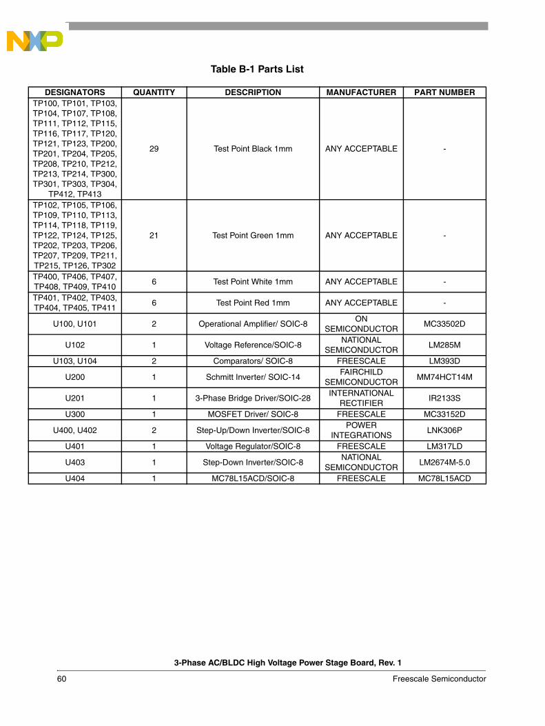
TP10TP10TP11TP11TP12TP20TP20TP21TP30
TTP10TP10TP11TP12TP20TP20TP2TP40TP4TP40TP4
D
0, TP101, TP103, 4, TP107, TP108, 1, TP112, TP115, 6, TP117, TP120, 1, TP123, TP200, 1, TP204, TP205, 8, TP210, TP212, 3, TP214, TP300, 1, TP303, TP304, P412, TP41329 Test Point Black 1mm ANY ACCEPTABLE -
2, TP105, TP106, 9, TP110, TP113, 4, TP118, TP119, 2, TP124, TP125, 2, TP203, TP206, 7, TP209, TP211,
15, TP126, TP302
21 Test Point Green 1mm ANY ACCEPTABLE -
0, TP406, TP407, 08, TP409, TP410
6 Test Point White 1mm ANY ACCEPTABLE -
1, TP402, TP403, 04, TP405, TP411
6 Test Point Red 1mm ANY ACCEPTABLE -
U100, U101 2 Operational Amplifier/ SOIC-8ON
SEMICONDUCTORMC33502D
U102 1 Voltage Reference/SOIC-8NATIONAL
SEMICONDUCTORLM285M
U103, U104 2 Comparators/ SOIC-8 FREESCALE LM393D
U200 1 Schmitt Inverter/ SOIC-14FAIRCHILD
SEMICONDUCTORMM74HCT14M
U201 1 3-Phase Bridge Driver/SOIC-28INTERNATIONAL
RECTIFIERIR2133S
U300 1 MOSFET Driver/ SOIC-8 FREESCALE MC33152D
U400, U402 2 Step-Up/Down Inverter/SOIC-8POWER
INTEGRATIONSLNK306P
U401 1 Voltage Regulator/SOIC-8 FREESCALE LM317LD
U403 1 Step-Down Inverter/SOIC-8NATIONAL
SEMICONDUCTORLM2674M-5.0
U404 1 MC78L15ACD/SOIC-8 FREESCALE MC78L15ACD
Table B-1 Parts List
ESIGNATORS QUANTITY DESCRIPTION MANUFACTURER PART NUMBER
3-Phase AC/BLDC High Voltage Power Stage Board, Rev. 1
60 Freescale Semiconductor
Appendix C. 3-Phase AC/BLDC High Voltage Power Stage Board Layouts
3-Phase AC/BLDC High Voltage Power Stage Board, Rev. 1
Freescale Semiconductor 61
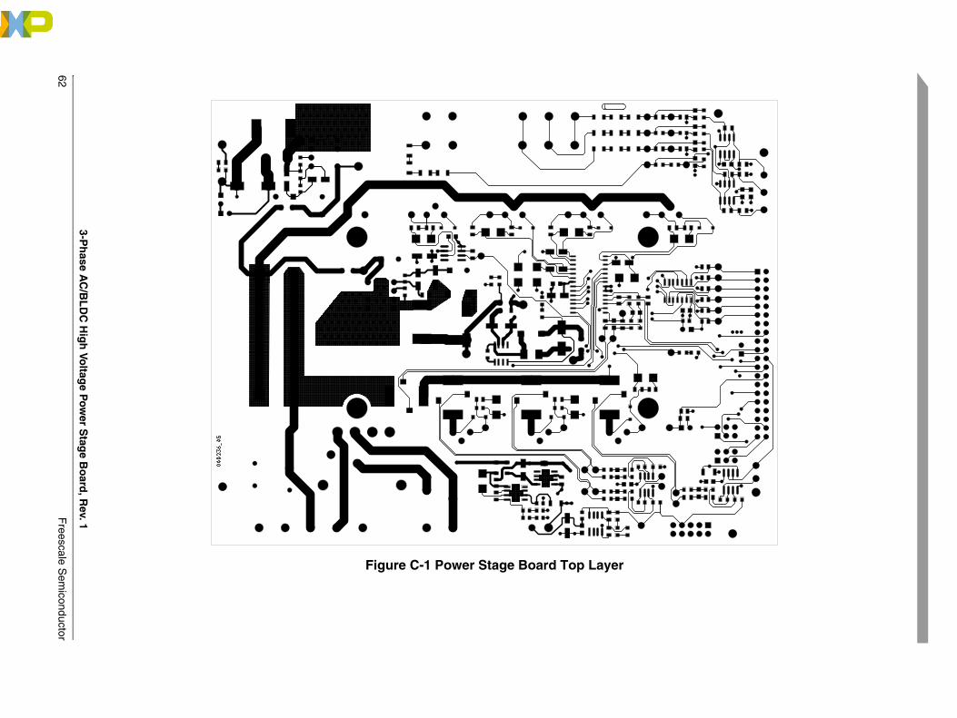
62F
reescale Sem
iconductor
3-Ph
ase AC
/BL
DC
Hig
h Vo
ltage P
ower S
tage B
oard
, Rev. 1
Figure C-1 Power Stage Board Top Layer
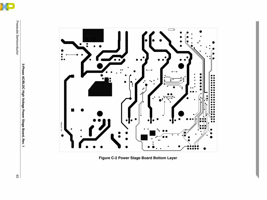
Freescale S
emiconductor
63
3-Ph
ase AC
/BL
DC
Hig
h Vo
ltage P
ower S
tage B
oard
, Rev. 1
Figure C-2 Power Stage Board Bottom Layer
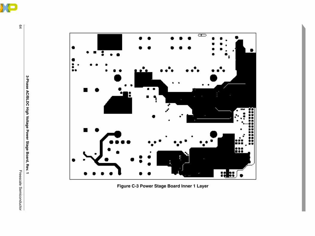
64F
reescale Sem
iconductor
3-Ph
ase AC
/BL
DC
Hig
h Vo
ltage P
ower S
tage B
oard
, Rev. 1
Figure C-3 Power Stage Board Inner 1 Layer
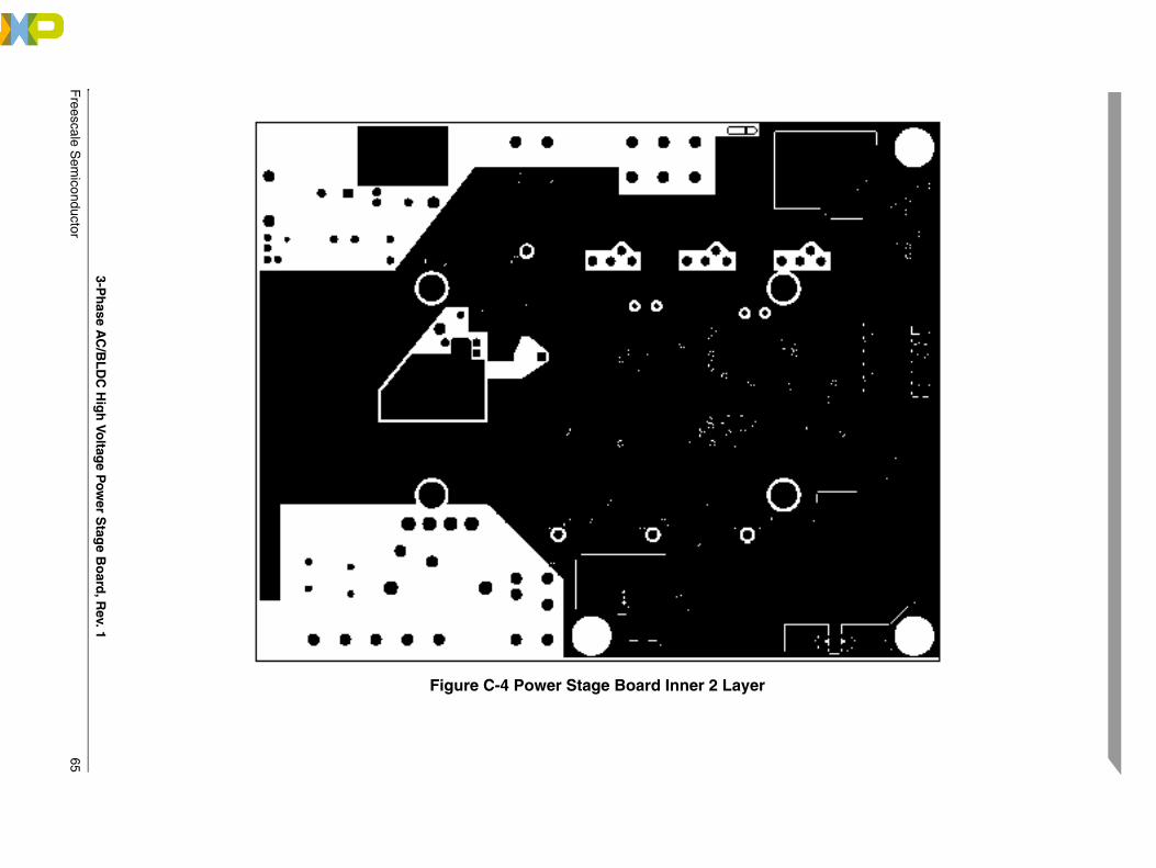
Freescale S
emiconductor
65
3-Ph
ase AC
/BL
DC
Hig
h Vo
ltage P
ower S
tage B
oard
, Rev. 1
Figure C-4 Power Stage Board Inner 2 Layer
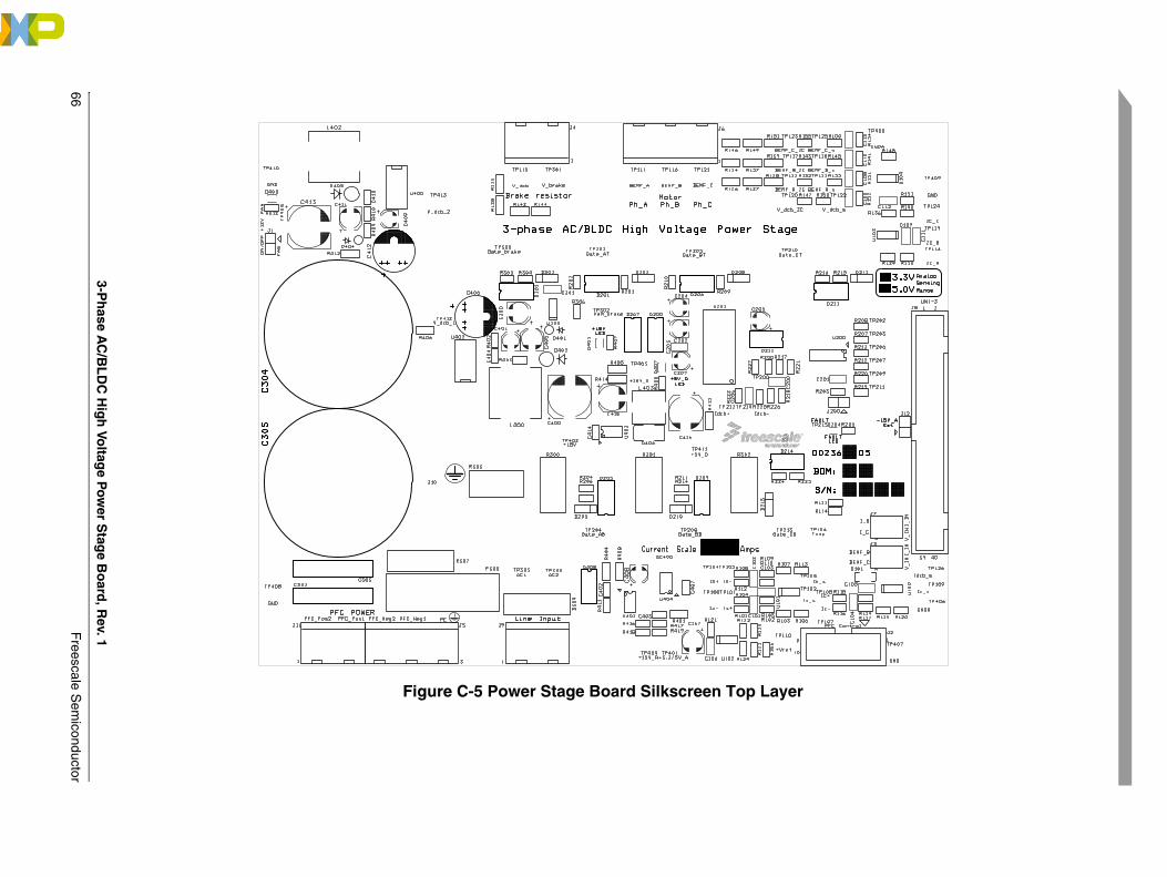
66F
reescale Sem
iconductor
r
3-Ph
ase AC
/BL
DC
Hig
h Vo
ltage P
ower S
tage B
oard
, Rev. 1
Figure C-5 Power Stage Board Silkscreen Top Laye
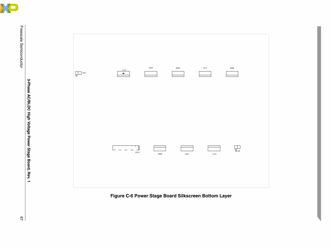
Freescale S
emiconductor
67
er
3-Ph
ase AC
/BL
DC
Hig
h Vo
ltage P
ower S
tage B
oard
, Rev. 1
Figure C-6 Power Stage Board Silkscreen Bottom Lay

3-Phase AC/BLDC High Voltage Power Stage Board, Rev. 1
68 Freescale Semiconductor

How to Reach Us:
Home Page:www.freescale.com
E-mail:[email protected]
USA/Europe or Locations Not Listed:Freescale SemiconductorTechnical Information Center, CH3701300 N. Alma School Road Chandler, Arizona 85224 +1-800-521-6274 or [email protected]
Europe, Middle East, and Africa:Freescale Halbleiter Deutschland GmbHTechnical Information CenterSchatzbogen 781829 Muenchen, Germany+44 1296 380 456 (English)+46 8 52200080 (English)+49 89 92103 559 (German)+33 1 69 35 48 48 (French)[email protected]
Japan:Freescale Semiconductor Japan Ltd. HeadquartersARCO Tower 15F1-8-1, Shimo-Meguro, Meguro-ku,Tokyo 153-0064, Japan0120 191014 or +81 3 5437 [email protected]
Asia/Pacific:Freescale Semiconductor Hong Kong Ltd.Technical Information Center 2 Dai King Street Tai Po Industrial Estate Tai Po, N.T., Hong Kong +800 2666 [email protected]
For Literature Requests Only:Freescale Semiconductor Literature Distribution CenterP.O. Box 5405Denver, Colorado 802171-800-441-2447 or 303-675-2140Fax: [email protected]
Information in this document is provided solely to enable system and software implementers to use Freescale Semiconductor products. There are no express or implied copyright licenses granted hereunder to design or fabricate any integrated circuits or integrated circuits based on the information in this document.
Freescale Semiconductor reserves the right to make changes without further notice to any products herein. Freescale Semiconductor makes no warranty, representation or guarantee regarding the suitability of its products for any particular purpose, nor does Freescale Semiconductor assume any liability arising out of the application or use of any product or circuit, and specifically disclaims any and all liability, including without limitation consequential or incidental damages. “Typical” parameters that may be provided in Freescale Semiconductor data sheets and/or specifications can and do vary in different applications and actual performance may vary over time. All operating parameters, including “Typicals”, must be validated for each customer application by customer’s technical experts. Freescale Semiconductor does not convey any license under its patent rights nor the rights of others. Freescale Semiconductor products are not designed, intended, or authorized for use as components in systems intended for surgical implant into the body, or other applications intended to support or sustain life, or for any other application in which the failure of the Freescale Semiconductor product could create a situation where personal injury or death may occur. Should Buyer purchase or use Freescale Semiconductor products for any such unintended or unauthorized application, Buyer shall indemnify and hold Freescale Semiconductor and its officers, employees, subsidiaries, affiliates, and distributors harmless against all claims, costs, damages, and expenses, and reasonable attorney fees arising out of, directly or indirectly, any claim of personal injury or death associated with such unintended or unauthorized use, even if such claim alleges that Freescale Semiconductor was negligent regarding the design or manufacture of the part.
Freescale™ and the Freescale logo are trademarks of Freescale Semiconductor, Inc. All other product or service names are the property of their respective owners. The ARM POWERED logo is a registered trademark of ARM Limited. ARM7TDMI-S is a trademark of ARM Limited. Java and all other Java-based marks are trademarks or registered trademarks of Sun Microsystems, Inc. in the U.S. and other countries. The Bluetooth trademarks are owned by their proprietor and used by Freescale Semiconductor, Inc. under license.© Freescale Semiconductor, Inc. 2004. All rights reserved.
3PHACBLDCHVPSUGRev. 101/2006