Embed Size (px)
Citation preview

216
Opposite Page:
Scanning electron micrograph of a patterned layer of amorphous Si, the first step in the process for fabricating the3-D photonic bandgap structure. (Courtesy of M. Qi)

217
Optoelectronics

218
Optoelectronics
• Development of Semiconductor Optical Devices for All-Optical Communication Networks
• Epitaxy on Electronics Integration Technology
• InGaAsP/GaAs Light Emitting Diodes Monolithically Integrated on GaAs VLSI Electronics
• Low Temperature Growth of Aluminum-Free InGaP/GaAs/InGaAs LED and Laser DiodeHeterostructures by Solid Source MBE using a GaP Cell
• Dry Etch Technology for Aluminum-free InGaP/GaAs/InGaAsLaser Diode Facets and Deflectors
• Development of High Speed Distributed Feedback (DFB) andDistributed-Bragg Semiconductor Lasers
• Monolithic Integration of Vertical-Cavity Surface-Emitting Laser Diodeson GaAs VLSI Electronics
• Microwave Characterization of Optoelectronic Devices
• The OPTOCHIP Project
• Monolithic Integration of 1550 nm Photodetectors on GaAs Transimpedance Amplifier Chips
• Normal-Incidence Quantum Well Intersubband Photodetectors (QWIPs)for Monolithic Integration
• One-Dimensional Photonic-Band-Gap Devices in SOI Waveguides
• Photonic Bandgap Structures
• Silicon Photonic Band Gap, Microcavity and Waveguide Structures
• Three-dimensional Photonic Bandgap Structures
• Design and Fabrication of an Integrated Channel-Dropping Filter in InP
• Fabrication of an Integrated Optical Grating-Based Matched Filter forFiber-Optic Communications
• Growth of Bandgap-Engineered Distributed Bragg Reflectors

219
Development of Semiconductor Optical Devices forAll-Optical Communication Networks
PersonnelL. A. Kolodziejski, E. P. Ippen, H. I. Smith, J. G. Fujimoto, H. A. Haus, M. S. Goorsky - University of California, LA, G. S. Petrich,K. L. Hall, G. Steinmeyer, B. E. Bouma, J. N. Damask, E. M. Koontz, J. M. Milikow, S. C. Warnick, I. P. Bilinsky, D. J. Jones, E. R.Thoen, T. E. Murphy, M. J. Khan, M. H. Lim, and K. M. Matney and G. D. U’Ren - University of California, LA
SponsorshipMIT Lincoln Laboratory and MURI/AFOSR
With the next generation of all-optical networks beingdesigned for operation at speeds of 100 Gbits/sec, theintegration of compact, efficient semiconductor-basedoptical devices offers many advantages. In these high bit-rate networks, low-loss wavelength-selective routingdevices and ultrafast optical pulse sources are required.
Waveguide-coupled Bragg-resonant filters provide acompact means of achieving high-density wavelength-selective routing. The functionality of the planar versionof these filters is contingent upon the ability to preservethe as-fabricated rectangular-patterned Bragg gratingsduring the gas source molecular beam epitaxial over-growth; deviations from the rectangular-grating profileresult in the inability to selectively route the desiredwavelength. Rectangular-patterned gratings, similar indimension to those required by the Bragg-resonant filters,have been fabricated in both InP and InGaAsP. An in-situlow temperature atomic hydrogen-assisted oxide removaltechnique has been employed to preserve the rectangulargrating profile. While the hydrogen-cleaned gratingappears to be intact as observed by scanning electronmicroscopy, the thermally-cleaned grating has experi-enced profile degradation in the form of rounded gratingteeth and filled-in grating trenches.
Triple Axis X-ray Diffractometry (TAD) has been used toprovide a nondestructive, high resolution analysis of theovergrown gratings. The (004) TAD reciprocal spacemaps of InGaAsP deposited on an InP grating reveal thehigh quality of the InGaAsP epilayer, the presence of aperiodic modulation within the overgrown structure asindicated by the existence of satellite reflections and thepresence of strain within the structure. The separation ofthe satellite reflections is related to the period of thegrating, and corresponds to an as-fabricated period of 230nm. The (224) TAD reciprocal space maps confirm thatstrain is present within the grating region, and isorthorhomically distorting the crystal. The magnitude of
the strain is on the order of 10-3, and is expected to have aminimal effect on the optical characteristics of the Bragg-resonant filters.
Currently, passive mode-locking of lasers is the mostpractical method of generating ultrashort (femtosecond)pulses. Saturable Bragg Reflectors (SBRs) provide aviable means for passive mode-locking a wide variety ofsolid state lasers. A SBR consists of a saturable absorber(quantum wells within a half-wave layer or a bulk-likeepilayer) integrated with a highly reflective mirror[Distributed Bragg Reflector (DBR)]. By epitaxiallydepositing (via gas source molecular beam epitaxy) thesaturable absorber directly on the mirror, the need foradditional fabrication steps (i.e. thinning or removing thesubstrate beneath the saturable absorber and using indexmatching epoxy to attach a saturable absorber to acommercial mirror) is avoided. Additionally, by selectingthe reflectivity of the DBR, the SBR can then be used aseither a high reflector or an output coupler in the lasercavity. The SBR structures that have been fabricated todate, contain either two or four InGaAs quantum wellspositioned 15 nm from the top of, or centered within, theInP half-wave layer. The DBR contains 22 pairs ofquarter-wave AlAs/GaAs layers, resulting in areflectivity spectrum centered at 1.55 µm. Two SBRs,both with two InGaAs quantum wells positioned 15 nmfrom the top of the InP half-wave layer, have successfullymode-locked a Cr4+:YAG laser. Since mode-locked fiberlasers offer a number of advantages over other ultrafastsources: compactness, the ability to be pumped with low-power laser diodes, a wavelength of operation centered atthe erbium-doped fiber gain peak of 1.55 µm and ease ofintegration into all-optical fiber networks, SBRs arecurrently being fabricated for implementation in erbium-doped fiber ring and sigma laser cavities as well as linearfiber cavities containing an erbium/ytterbium co-dopedamplifier. ❏

220
Epitaxy on Electronics Integration Technology
PersonnelJ. Ahadian, Y. Royter, S. G. Patterson, and P. T. Viadyananthan(C. G. Fonstad, Jr., L. A. Kolodziejski, G. Petrich, P. A. Postigo, J. M. Mikkelson, and Dr. W. Goodhue)
SponsorshipJSEP/RLE, ARPA/NCIPT, NSF, Lincoln Laboratory,and ONR
The development of optical interconnects has beenhampered by the lack of a viable source of complexOptoelectronic Integrated Circuits (OIECs), circuitswhich will ultimately need to contain thousands ofoptoelectronic devices tightly integrated with VLSI-complexity electronics. Hybriding, wafer-bonding, andepitaxial lift-off have made progress in addressing thisneed, however issues of density performance, reliability,and yield suggest that monolithic integration is the bestanswer, as it has been in conventional microelectronicsmanufacturing. To answer this need we have developeda process, termed Epitaxy-on-Electronics (EoE), formonolithically integrating optoelectronic devices oncommercially processed gallium arsenide ICs.
The EoE process begins with custom-designed GaAsVLSI circuits. The electronics technology (the VitesseSemiconductor HGaAs3 Process) provides enhance-ment- and depletion-mode MESFETs and four layers ofaluminum-based electrical interconnect, as well asOptical Field-Effect Transistor (OPFET) and metal-semiconductor-metal (m-s-m) photodetectors. Molecu-lar Beam Epitaxy (MBE) is used to grow deviceheterostructures on regions of the GaAs substrate whichare exposed by cutting through the interconnect dielec-tric stack. Established fabrication techniques completethe integration procedure. The unrestricted placementof the optoelectronic devices occurs as part of the routinelayout of the integrated circuit; the interconnect dielec-tric stack in the regions designated for these devices ispartially etched at the GaAs foundry forming DielectricGrowth Windows (DGWs). The etch is completed,exposing the underlying GaAs substrate, upon receipt ofthe ICs from the manufacturer; the design of the DGWstructure and of the technique for producing a damage-free GaAs starting surface are among the latest innova-tions in the EoE process. The source/drain implant isused as the bottom n-contact of the optoelectronicdevice. Epitaxial material is then grown in the DGWs,while polycrystalline material is deposited on theoverglass. Standard processing techniques are then used
to remove the polycrystalline material, to fabricate theoptoelectronic devices, and to interconnect the top-sideelectrical contacts of the devices to the electronics.
As in standard silicon technologies, the gallium arsenideVLSI process uses aluminum-based electrical intercon-nects. We have shown that these interconnects degradewhen exposed to temperatures in excess of 475° C.Conventional MBE practice uses a 580° C temperatureexcursion to desorb the native oxide on the GaAs surfaceprior to growth, and even this brief high temperatureexposure (which was used in previous EoE work) resultsin appreciable damage to the interconnect lines. Inter-connect degradation is now effectively eliminated byusing cracked hydrogen to remove the native oxide aslow as 350° C.
Also owing to the electrical interconnect thermal instabil-ity, the epitaxy must be carried out below 475° C. Thisrestriction is not compatible with the growth of highquality AlGaAs suitable for emitters (although it can beused in passive applications) due to aluminum’s highaffinity for oxygen. The performance of previousmonolithic EoE light emitting diodes involving AlGaAsheterostructures was thus compromised. To circumventthis difficulty, current EoE efforts use the aluminum-freeInGaAsP materials system, which is routinely grown areduced temperatures.
Process innovations in the areas of DGW preparation,low temperature GaAs native oxide removal, and gas-source MBE growth of EoE compatible optoelectronicdevices have removed limitations present in previousEoE demonstrations. Ring oscillator measurementsmade before and after EoE processing have verifiedstable sub-100 picosecond gate delays, consistent withsub-nanosecond, multi-gigahertz electronics operation.The present EoE technology is now being applied to avariety of applications benefiting from the integration ofhigh performance heterostructure devices with VLSI-complexity electronics. ❏

221
InGaAsP/GaAs Light Emitting Diodes Monolithically Integratedon GaAs VLSI Electronics
PersonnelP. T. Viadyananthan, J. Ahadian, S. G. Patterson, and Y. Royter(C. G. Fonstad, Jr., L. A. Kolodziejski, S. Prasad, G. Petrich, and P. A. Postigo)
SponsorshipDARPA/NCIPT, ONR, and NSF
While surface-emitting lasers are ultimately desired inoptical interconnect applications because of their largebandwidth, efficiency, and directionality, recent EoEwork has been restricted to the integration of LEDs, withcomparatively relaxed growth and fabrication demands,in order to focus attention on the EoE-specific processdevelopment. Mesa-confined GaAs/InGaP double-heterostructure LEDs are used in this demonstration ofmonolithic, emitter-based OEICs.
LEDs are fabricated following epitaxy and removal ofthe polycrystalline deposits. The fabrication process isnearly identical to that of similar devices on bulk wafers.The primary difference is in the use of thick photoresists(3 to 4 µm) which are needed in order to assure step-coverage over chip-surface non-planarities. Contactlithography is readily used to pattern 2 to 3 µm mini-mum feature sizes. Step coverage also requires the useof aluminum interconnect metalization. To avoid theundesirable reaction of aluminum with a gold-basedohmic contact, Ti/Pt ohmic contacts are used.
An Al interconnect line links the Ti/Au/Ni p-contact tonearby electronics. An optical shield around the DGWperimeter is formed by stacking interconnect metals upto Metal-3. The purpose of this shield is to preventcoupling of LED emission to nearby electronics. Twoshield designs (referred to as #1 and #2) differing in thesizing and placement of metal and via patterns, andconsequently differing in surface non-planarity abovethe shield, were implemented around 50 µm DGWs.Unshielded 85 µm DGWs were also used.
The nominal LED emission wavelength is 873 nm,corresponding to the bandgap of the GaAs core. Theangular distribution of the output light is Lambertian,i.e., intensity proportional to the cosine of the normalangle.
Operation of the LED-based OEICs can be illustratedthrough the example of a simple “optical inverter” on thechip. The input element is an OPFET. With no appliedlight, the OPFET is in its off state and pulls the output ofan inverter loading it to the DCFL high level of 0.6 V.Following three inversions, the signal arrives at the gateof a pull-down EFET as a low. The drain of this off-stateEFET rises to 3 V, and 2 V remains across the LED. Thereis no significant LED current and the optical output isoff. When the incident power reaches just above 0.1 µW,the OPFET switches on. The inverter output is nowpulled to a DCFL low level of 0.1 V. This signal cascadesthrough the three inverter stages and turns on the pull-down EFET. The drain of this EFET now drops to 0.8 V.With 4.2 V across the LED, the EFET sinks 4.6 mA ofcurrent corresponding to an optical output power of2 µW. This power level is 13 dB above the 0.1 µW opticalinput threshold. This level of optical gain allows EoE-integrated LED-based OEIC to meet the realistic systemrequirements of many optical interconnect architectures.In fact, this 13 dB figure represents a lower bound on theoptical gain achievable with these OEICs. Use of an85 µm DGW LED would increase this optical gain toroughly 20 dB. ❏

222
Low Temperature Growth of Aluminum-Free InGaP/GaAs/InGaAs LED andLaser Diode Heterostructures by Solid Source MBE using a GaP Cell
PersonnelP. A. Postigo(C. G. Fonstad, Jr. and D. Braddock)
SponsorshipLincoln Laboratory
The use of InGaP instead of AlGaAs for the fabrication oflight emitting heterostructures as Light Emitting Diodes(LEDs) and Laser Diodes (LDs) presents importantadvantages, such as the reduction of deep donor levelsand lower InGaP/GaAs interface recombination velocity.In addition, InGaP is more suitable for the reduced-temperature Molecular Beam Epitaxy (MBE) required forthe Epitaxy-on-Electronics integration technology(475° C), since it is aluminum-free.
The use of phosphorous in MBE has traditionally beendone through the introduction of phosphine (PH3) as agaseous source. However, the use of a solid source is alsovery attractive since it is easier to implement and tomaintain in the MBE system, but it must be a solid sourcewhich gives a very high ratio of dimers to tetramers, i.e.,P2 to P4 . The dimers have a higher sticking coefficientand are much better for MBE growth. Two methods havebeen used to produce P2 from solid sources. One is basedin a two-zone-cracker cell where the P4 is cracked in P2 bya very high temperature section (>1000° C), and wherethe source is solid red-phosphorous. The other method isbased on the sublimation of phosphorous from phos-phides as GaP, which produces the best P2 to P4 rate(around 170 compared to the 3.5 to 6 of the thermalcracker). The GaP decomposition cell has the samedesign as a common group-III effusion cell that operatesat high temperatures (the typical temperature used forphosphide growth is around 1000°C) and it can beoperated as a regular group-III cell. However, this typeof cell can produce some residual amount of Ga, that canbe reduced through an special design. This designimplements a dome-shaped and disk-shaped PyrolyticBoron Nitride (PBN) cap on top of the normal crucible,that acts as a trap for the Ga atoms. In collaboration withDr. David Braddock, from EScience Inc., we have success-fully demonstrated a high-capacity (100 gr) GaP decom-position source that has produced high quality epitaxialInP and InGaP. The epilayers have been analyzed byDouble-Crystal X-ray Diffraction (DCXR),
PhotoLuminescence spectroscopy (PL), and SecondaryIon Mass Spectroscopy (SIMS). The high purity of the P2beam obtained through this method and the goodbehavior of the cell have been used to produce InP/InGaAs photodetectors and InGaP/GaAs/InGaAs LEDsheterostructures at low growth temperature (475° C).Further work will focus on using this P2 source forreduced-temperature growth of InGaP/GaAs/InGaAslaser diodes for integration on GaAs VLSI chips usingthe Epitaxy-on-Electronics process. ❏

223
Dry Etch Technology for Aluminum-free InGaP/GaAs/InGaAsLaser Diode Facets and Deflectors
PersonnelY. Royter and J. Ahadian(C. G. Fonstad, Jr., P. A. Postigo, W. Goodhue, and D. Mull)
SponsorshipLincoln Laboratory
Aluminum-free InGaAsP/GaAs/InGaAs laser diodesare receiving a great deal of attention currently becauseof their superior performance and reliability in compari-son to more conventional AlGaAs/GaAs/InGaAs laserdiodes. Our own interest in these devices is driven bytheir compatibility with the Epitaxy-on-Electronics (EoE)monolithic optoelectronic integration technology we aredeveloping (described elsewhere in this report). Inparticular, high quality aluminum-free laser diodes canbe grown at temperatures below 475° C, which arecompatible with the EoE technology whereas laserdiodes with aluminum in or near their active regions cannot be grown at such low temperatures.
An important challenge with aluminum-freeheterostructures is dry etching vertical end-mirror facetsand angled deflector structures, because of the verydifferent chemical make-up of the layers. In particular,the wider bandgap InGaAsP layers contain significantamounts of In and P, and relatively little or no As,whereas the narrow-gap GaAs and InGaAs layerscontain roughly 50% As, no P, and relatively little or noIn. Conventional chlorine-based and methane-based dryetch techniques do not work well with the aluminum-free heterostructures. We find, for example, that ion-beam assisted chlorine etching of InGaP is very slow atroom temperature; at elevated temperatures where theInGaP etches satisfactorily, GaAs layers are etchedwithout the need for the ion beam and severe lateraletching occurs, i.e., the etch is not directional and notanisotropic. While we can make use of this feature in theEoE process for removing polycrystalline deposits, it isnot useful for facet etching.
The solution to this problem lies in changing the etchantfrom chlorine to bromine because the vapor pressures ofthe relevant bromides are much more similar than arethose of the corresponding chlorides. Consequently, it ispossible to find etch conditions for which the etch ratesof InGaP and GaAs are sufficiently similar that vertical
mirror facets can be successfully etched. We have usedthese results to produce the first etched-facet alumi-num-free laser diodes. The threshold current densitiesof broad-area etched-facet laser diodes are a factor oftwo higher than adjacent cleaved-facet lasers.
The performance of the current etched-facet lasers islimited primarily by the quality of the etch mask, whichwe feel is in turn limited by the aligner used. Conse-quently a 4x projection aligner has been acquired for useon this program and preliminary indications are that itsuse significantly improves mask quality, i.e., edgedefinition and smoothness. Future work will combinethis new tool with continued work refining the etchchemistry through the combination of both chlorine andbromine in the ion-beam assisted etch system (which islocated in MIT’s Lincoln Laboratory). A heated, rotat-able substrate stage has also been installed on thesystem in preparation for work on etching curveddeflectors. These, along with the vertical end facets, arethe key to producing the In-Plane, Surface-EmittingLasers (IPSELs) we propose to integrate on GaAsintegrated circuit chips using the Epitaxy-on-Electronics(EoE) process. ❏
224
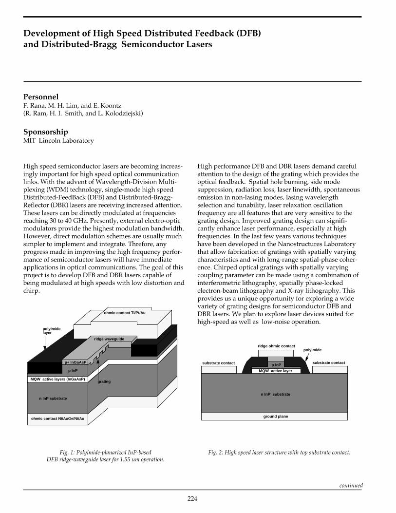
Development of High Speed Distributed Feedback (DFB)and Distributed-Bragg Semiconductor Lasers
PersonnelF. Rana, M. H. Lim, and E. Koontz(R. Ram, H. I. Smith, and L. Kolodziejski)
SponsorshipMIT Lincoln Laboratory
High speed semiconductor lasers are becoming increas-ingly important for high speed optical communicationlinks. With the advent of Wavelength-Division Multi-plexing (WDM) technology, single-mode high speedDistributed-FeedBack (DFB) and Distributed-Bragg-Reflector (DBR) lasers are receiving increased attention.These lasers can be directly modulated at frequenciesreaching 30 to 40 GHz. Presently, external electro-opticmodulators provide the highest modulation bandwidth.However, direct modulation schemes are usually muchsimpler to implement and integrate. Threfore, anyprogress made in improving the high frequency perfor-mance of semiconductor lasers will have immediateapplications in optical communications. The goal of thisproject is to develop DFB and DBR lasers capable ofbeing modulated at high speeds with low distortion andchirp.
High performance DFB and DBR lasers demand carefulattention to the design of the grating which provides theoptical feedback. Spatial hole burning, side modesuppression, radiation loss, laser linewidth, spontaneousemission in non-lasing modes, lasing wavelengthselection and tunability, laser relaxation oscillationfrequency are all features that are very sensitive to thegrating design. Improved grating design can signifi-cantly enhance laser performance, especially at highfrequencies. In the last few years various techniqueshave been developed in the Nanostructures Laboratorythat allow fabrication of gratings with spatially varyingcharacteristics and with long-range spatial-phase coher-ence. Chirped optical gratings with spatially varyingcoupling parameter can be made using a combination ofinterferometric lithography, spatially phase-lockedelectron-beam lithography and X-ray lithography. Thisprovides us a unique opportunity for exploring a widevariety of grating designs for semiconductor DFB andDBR lasers. We plan to explore laser devices suited forhigh-speed as well as low-noise operation.
n InP substrate
MQW active layers (InGaAsP)
polyimidelayer
p+ InGaAsP
grating
ridge waveguide
ohmic contact Ti/Pt/Au
ohmic contact Ni/AuGe/Ni/Au
p InP
n InP substrate
p InP
MQW active layer
ridge ohmic contact
substrate contact substrate contact
ground plane
polyimide
Fig. 1: Polyimide-planarized InP-basedDFB ridge-waveguide laser for 1.55 um operation.
Fig. 2: High speed laser structure with top substrate contact.
continued

225
We have developed techniques for fabricating highspeed polyimide-planarized ridge-waveguide laserstructures that have low capacitance and are thereforeideally suited for high frequency operation. A crosssection of an InP based DFB laser is shown in Figure 1.The active layers consist of multiple InGaAsP quantumwell layers. The grating is etched in InP, and InGaAsP isregrown on top. The ridge is etched and then planarizedusing polyimide. Ohmic contact to the ridge is made byliftoff on top of the polyimide layer. RC roll off is one ofthe most important factors that limit the high frequencyperformance of lasers. The thick layer of polyimidereduces significantly the capacitance between the topmetal electrode and the substrate. In addition to thisstructure, we are also exploring laser structures with co-planar microwave striplines for the ridge and substrateohmic contacts. This is illustrated in Figure 2. This designoffers improved high frequency performance and lowseries resistance. ❏
continued
continued
Monolithic Integration of Vertical-Cavity Surface-Emitting Laser Diodeson GaAs VLSI Electronics
PersonnelH. Choy(C. G. Fonstad, Jr. and R. Ram)
SponsorshipNSF and Lincoln Laboratory
Vertical-Cavity Surface-Emitting Lasers (VCSELs) areparticularly suitable as light sources for optoelectronicsintegration technologies, such as our Epitaxy-on-Elec-tronics (EoE) process. The compact, vertical geometryand the completely epitaxial growth of VCSELs makemass fabrication and testing convenient and economical.The small size of the active region results in low thresh-old currents. Finally, the surface-emitting propertyresults in an excellent beam profile of the emission, whichsimplifies coupling to optical fibers. VCSELs are emerg-ing as ideal light emitters for high-density free-spaceinterconnection.
VCSELs consist of several active quantum wells, sand-wiched between two highly reflective Distributed BraggReflectors (DBRs). These DBRs are realized by epitaxialgrowth of AlGaAs layers, lattice-matched to GaAs, withvarying aluminum and gallium compositions.
The production of VCSELs is not without its own set ofchallenges. Unlike in-plane semiconductor lasers, light inVCSELs resonates in the direction perpendicular to thethin quantum wells. In order to achieve laser action, thequantum wells must have high radiative efficiency andbe situated inside a cavity with a high Q-factor. Thisrequires the DBRs to have very high reflectivities and lowtotal losses; they typically consist of many periods.Several design and growth concerns are important: First,the large number of layers creates numerousheterojunctions which require careful design such thatthe impedance of the whole device is minimized, and thethreshold current and operating voltage remain low.Second, the growth conditions need to be controlledprecisely while the structure is being grown, whichtypically takes four to five hours. Finally, thereflectivities of the top and bottom mirrors need to becarefully designed to strike a balance between high Q-factor and high external efficiency.

226
continued Microwave Characterization ofOptoelectronic Devices
PersonnelP. T. Viadyananthan(C. G. Fonstad, Jr. and S. Prasad)
SponsorshipDARPA/NCIPT and NSF
The microwave device characterization capability hasbeen expanded so that optoelectronic devices may becharacterized using the automatic network analyzer andthe on-wafer probe station. The objective was to do acomplete characterization of the high speed performanceof Light Emitting Diodes (LED’s) both discrete andintegrated on chip. The aim of e preliminary measure-ments was to model the high frequency behavior of theLED’s and to determine the frequency limits of thedesired characteristics. A comparison of the behavior ofdiscrete and integrated devices is important to theunderstanding of the issues that are unique to theepitaxy-on-electronics integration technology. Anaccurate estimation of device performance together withphysical modeling will result in the efficient applicationof LED’s as emitters in OEIC’s and will be the basis ofproposed future investigations of high speed surface-emitting lasers.
To this end, measurements were performed on discreteLED’s and LED’s integrated on the OPTOCHIP. Themicrowave reflection and transmission properties of theLED’s were measured using the HP 8753C networkanalyzer with a frequency range of 300 kHz to 3 GHz.This range was appropriate for the test devices whichoperated at frequencies under 3 GHz. The DC bias isapplied with an HP 4145B semiconductor parameteranalyzer. The optical output from the LED is collectedby a high bandwidth detector which is placed close tothe emission field of the LED to improve the collectionefficiency. A Hamamatsu S5972 p-i-n photodiode with a3 dB bandwidth of 500 MHz was used as a detector. Theelectrical signal from the detector was amplified using ahigh frequency amplifier. The scattering parameterswere measured using this experimental arrangement.
Presently, the goal is to achieve flat-bands for carriers inthe DBR mirrors as part of the effort to arrive at a lowthreshold current. This can be achieved by graduallychanging the aluminum and gallium compositions witha parabolic profile across the interfaces, while simulta-neously maintaining the doping in the span of thegrading regions at a much higher level than in the rest ofthe mirror stack. We focus our effort on p-type topmirrors, since holes have an effective mass eight timesmore than that of electrons, and thus are much morevulnerable to potential barriers at the heterojunctioninterfaces.
The optimal design for the grading regions is a compro-mise between a short enough length and a adequatelygradual grading. Short grading regions lower the freecarrier absorption resulting from the high doping leveland maintain a high overall DBR reflectivity. Gradualgrading yields lower impedance mirrors with smallerdoping level. The transient behavior of the cells has alsoto be studied to determine maximum grading speed,because effusion cells used in MBE systems cannotcontrol the flux accurately when the change is too fast.
VCSELs grown on bulk GaAs under normal growthconditions and in-plane lasers with similar quantumwells will be fabricated to compare basic materialqualities and growth capabilities. We will also assessthe impact of a reduced growth-temperature on the gainof the active region and on the conductivity of the DBRmirrors. This is critical for the adoption of this structureto our EoE technology. ❏
continued

227
Current-voltage (I-V) and light-current (L-I) characteris-tics were measured initially for a DC analysis. Withreverse bias, the bulk devices had a higher leakagecurrent than the integrated devices. It was concludedthat lateral confinement was provided by dielectricgrowth wells in the integrated device on OPTOCHIP.With forward bias, both types of LED’s show a turn-oncurrent which is larger than expected. A 4-elementmodel has been proposed to describe these effects Themodel explains the observed diode characteristics andindicates that the difference in turn on currents isassociated with material quality. The difference inefficiencies is due to the different values of the non-radiative recombination coefficient and bimolecularrecombination coefficient in the devices measured.
Since the LED is a two terminal device, measurements ofS21 were used to determine the frequency response. ADC bias was applied to the LED and an RF signal wassuperimposed with enough RF power for small signalmodulation of the LED about the bias level. The biaswas varied and the response was measured at each biaslevel. The frequency response of bulk and integrateddevices was measured. The integrated devices onOPTOCHIP had a higher bandwidth than the bulkLED’s at comparable bias levels.
Our modeling indicates that the nominally undopedactive regions of the LED’s was in fact quite n-type, andthat significantly higher efficiency and bandwidth willbe obtained if the active region is made narrower and isintentionally doped p-type. Such design modificationswill be explored to enhance the performance of theLED’s. The investigations will then be extended toVertical Cavity Surface Emitting Lasers (VCSEL’s). ❏
continued The OPTOCHIP Project
PersonnelJ. Ahadian, S. G. Patterson, P. T. Viadyananthan,and Y. Royter (C. G. Fonstad, Jr., L. A. Kolodziejski,G. Petrich, P. A. Postigo, and J. M. Mikkelson)
SponsorshipDARPA/NCIPT and ONR
The OPTOCHIP Project is a research foundry offeringintended to provide prototype OEICs to selected univer-sity groups doing research on optical interconnectsystems. The first generation OPTOCHIPs use InGaP/GaAs Light Emitting Diodes (LEDs) monolithicallyintegrated using the Epitaxy-on-Electronics (EoE) tech-nology on commercially fabricated GaAs integratedcircuit chips containing OPtical Field Effect Transistor(OPFET) and Metal-Semiconductor-Metal (m-s-m)photodetectors, and enhancement- and depletion-modemetal-semiconductor field effect transistors (MESFETs).A solicitation for participation was made in late 1995 andin early 1996 nine groups from eight universities wereselected to participate; the universities represented areCalifornia Institute of Technology, Colorado StateUniversity, George Mason University, McGill University,Texas Christian University, University of SouthernCalifornia, and University of Washington. These groupsbegan work in February 1996 on the designs for 2 mm by2 mm OEIC chips which were combined into a larger dieand submitted to the MOSIS service in May 1996. Thechips were fabricated by Vitesse Semiconductor Corpora-tion, Camarillo, CA, in the summer and fall of 1996, andthe EoE integration process was initiated early in 1997.Fabrication of the integrated LEDs was completed inMay 1997, and the completed OPTOCHIP die were sewninto individual 2 mm by 2 mm chips and returned to thedesigners for deployment in their optical interconnectarchitectures.
Electrical tests on the completed OPTOCHIP die showthat there was no degradation in the electrical perfor-mance of the circuitry due to the EoE process. Theperformance and yield of the LEDs were poorer than hadbeen achieved on previous test runs, due it appears toproblems in the growth system, but several functionaldie were provided to each participating group. Theamount of work done with the completed chips variesbetween the various groups, but several groups haveperformed extensive testing of their OEIC chips and have
continued

228
successfully employed them in systems-level situations.In one case, communication between a pair ofOPTOCHIPs has been demonstrated. Work is continu-ing on the testing of the chips, and our group at MIT isworking to be able to supply the participants withanother set of die processed using the new GaP phospho-rous source recently installed on our MBE.
The completed, overall 7 mm by 7 mm squareOPTOCHIP die each contain over 200 LEDs integratedwith numerous different circuits and subsystems con-taining thousands of transistors. As such they representsome of the most complex LED-based monolithic OEICsever fabricated. The OPTOCHIP project was also uniquein that the OPTOCHIP die incorporate designs from adiverse selection of groups and in that minimal con-straints were placed on the circuit designs.
Our intention is that there will be future OPTOCHIPofferings, and that the processing of subsequentOPTOCHIPs will be done on a semi-professional basisusing the facilities of the Technology Research Labora-tory (TRL) of the Microsystems Technology Laboratory(MTL) at MIT. We are anxious to make Surface-EmittingLasers (SELs) available to OPTOCHIP users in the nearfuture; Self-Electro-optic Effect Devices (SEEDs) areanother option, but our primary focus is on emitter-based OEICs containing LEDs or SELs. ❏
Monolithic Integration of 1550 nmPhotodetectors on GaAsTransimpedance Amplifier Chips
PersonnelH. Wang(C. G. Fonstad, Jr., R. Hemenway, R. Deming,and J. Mikkelson)
SponsorshipMIT Lincoln Laboratory
High data rate optical communication systems requireincreasingly complex integration of high performanceelectronic circuits with sophisticated optoelectronicdevices. In the short run these needs can be met byhybrid assemblies. However the cost, performancecompromises, and reliability concerns associated withhybrid integration, and the increasing need for special-ized subcircuits which are not commercially available,make development of the monolithic integrated circuittechnology extremely desirable.
We are using several techniques to monolithicallyintegrate 1550 nm photodetectors with Gallium Arsenide(GaAs) TransImpedance Amplifiers (TIAs) to formmonolithic OptoElectronic Integrated Circuits (OEICs)for fiber-based systems. Both Epitaxy-on-Electronics(EoE), described elsewhere in this report, and selectivearea semiconductor wafer bonding, also describedelsewhere in this report, will be utilized. In the EoEprocess, optical devices are epitaxially grown on fullyprocessed GaAs integrated circuits. For this application,high-speed photodetectors based on the lattice-mis-matched InGaAs/GaAs material system are beingdeveloped and evaluated. For the wafer bondingprocess, fully lattice-matched photodetectorheterostructures, grown under optimal conditions onInP, will be bonded onto the same GaAs circuits. AfterEoE epitaxy or wafer bonding, the deviceheterostructures will be processed and monolithicallyintegrated with the pre-existing electronics, yieldinghigh speed, compact, reliable monolithic OEIC’S.
The GaAs transimpedance amplifier test chip (MIT-OEIC5/LL-MORX1), which incorporates modifiedversions of a commercial Vitesse transimpedanceamplifier, has been designed and submitted to MOSISfor processing. Included on this chip are polarizationdiversity heterodyne photoreceivers, dual-balancedphotoreceivers, and other functional cells; the chip iswhich are suitable for both EoE epitaxy and waferbonding.
continued
continued
229
Initial results from measurements on 1550 nm photodiodesgrown on GaAs have been obtained. The performance ofIn0.52Al0.48As/In0.53Ga0.47As pin photodiodes grown onGaAs substrates using linearly graded buffers were com-pared with those using graded short-period superlattice(GSSL) buffers. Detectors on linearly-graded buffer arefound to be superior to those on GSSL buffer. However, thebest dark current levels seen (5 µA for 50 µm squaredetectors at 2V bias) must to be reduced for final integra-tion.
Several approaches to the reducing the leakage are beinginvestigated simultaneously. A side-wall passivationtechnique using polyimide has been proposed and therequired mask set is being generated. A second method isto replace the wide gap InAlAs with electrically superiorInP. New heterostructures using InP as cladding layershave been grown and are being processed. Thirdly, wehave lowered the indium concentration grading rate from17% per micron to 10% per micron, aiming at loweringthreading dislocation density in the absorption layer.Finally, a novel structure, the Uni-Travelling-CarrierPhotodiode (UTC-PD), is being considered for both darkcurrent reduction and speed enhancement.
Optimized detector MBE growths have been carried out onboth n-GaAs and n-InP substrates for a comparative studyof the effects of lattice mismatch. Photodetectors will also begrown on p-InP substrates in order to be bond onto theGaAs chips. Wafer bonding using both direct bonding ofInP and InGaAs to GaAs by atomic rearrangement, andbonding with palladium assistance will be investigated.The method yielding the best electrical characteristics willbe chosen to bond the detectors onto OEIC5 chips.
Future work will expand the effort to include integration of1550 nm light emitters as well as detectors, which requiressignificant work on direct wafer bonding of InP-basedmaterials onto GaAs chips and/or work on high qualitylattice-mismatched InGaAs/InP epi-layers on GaAs. ❏
continued Normal-Incidence Quantum Well Inter-subband Photodetectors (QWIPs) forMonolithic Integration
PersonnelJ. Pan(C. G. Fonstad, Jr.)
SponsorshipNSF, ONR, and Lockheed-Martin
Band gap engineering allows us to design the peakresponsivity of a Quantum Well Intersubband Photode-tector (QWIP) to be at anywhere in the infrared regionbeyond about 2 µm. This wavelength region is useful forspectroscopy and identification of unknown gases, aswell as for imaging in the Earth’s atmosphere in thetransparent spectral regions of 3 to 5 µm and 8 to 12 µm.The narrow spectral responsivity of QWIPs allows forthe use of lenses, which are cheaper and smaller thanmirrors, in the optical systems used to focus infraredradiation onto the detectors. This flexibility in thelocation of the peak in the responsivity spectrum, as wellas the narrow spectral width of the responsivity, are alsouseful in he design of dual band and dual color QWIPs.Detection of the infrared radiation emanating from anobject at two different wavelengths makes it possible toascertain the absolute temperature of the object and todistinguish it from the “clutter” surrounding it.
Modern epitaxy techniques can achieve high uniformityof semiconductor parameters across entire III-V (GaAsand InP) wafers, which allows for the realization of largeFocal Plane Arrays (FPAs) of QWIPs with low spatial(fixed) pattern noise. Furthermore, the growth of QWIPson GaAs substrates is compatible with the monolithicintegration of QWIPs with standard GaAs detectorcircuits. Monolithic integration would remove the needfor indium bump bonding, an extra processing stepwhich contributes to increased expense and reducedyield, and monolithic integration is one of the importantobjectives of our program. Specifically, our goal is tofabricate QWIPs which can be monolithically integratedwith standard GaAs detector circuits using the Epitaxy-on-Electronics (EoE) process.
QWIPs which can respond to normally incident radiationwill eliminate the need for an optical grating and forthinning of the devices, thus simplifying the processingand increasing the processing yield for such devices.However, the intersubband absorption of normally
continued

230
incident radiation is in general very weak; it depends onthe size of the electron’s transverse wave vector or thesize of the bulk spin-orbit interaction. By paying specialattention to such issues we have successfully demon-strated the first n-type QWIP (n-QWIP) which respondsto normally incident radiation without the use of anoptical grating. Such QWIPs are observed to have aconversion efficiency of about 3%. While this is animportant result, the quantum efficiency of such devicescan be increased further by utilizing a transition whichexhibits even stronger absorption of normally incidentradiation. We are currently investigating strained,pseudomorphic p-type QWIPs for this purpose.
Whereas tactical missions in the past have required focalplane arrays to detect targets which are brighter than thebackground, with about 1016 photons/cm2-s reachingthe detector, recently, there has been a shift in theapplications of quantum well infrared photodetectorstowards detection in space of faint targets at largedistances of several thousand kilometers with onlyabout 1013 photons/cm2-s reaching the detectors.Future work on QWIPs must not only focus on increas-ing the photoconductor conversion efficiency, but alsoon the more stringent requirements on FPA uniformity,linearity, and dark current of such applications. Fainttargets require larger pixel sizes and better uniformityacross the fewer pixels. Better linearity is also needed insituations where absolute radiometry is required.Device modeling is now being carried out in an effort toincrease the ratio of the photocurrent to the dark currentby increasing the ratio of the photoconductive gain todark current gain. ❏
continued One-Dimensional Photonic-Band-GapDevices in SOI Waveguides
PersonnelS. Fan, J. Ferrera, J. S. Foresi, G. Steinmeyer, E. R. Thoen,and P. R. Villeneuve (E. P. Ippen, J. D. Joannopoulos,L. C. Kimerling, and H. I. Smith)
SponsorshipNSF and JSEP
Photonic Band Gap (PBG) structures are optical analogsof semiconductors. A light wave traveling through a PBGstructure encounters a large, periodic change in thedielectric constant. The periodicity causes bands offrequencies to be disallowed from propagating throughthe structure. These bands can be as large as 30 percent ofthe mid-gap frequency. PBG’s can be designed in 1-, 2-,and 3-dimensions. 1-D PBG’s are similar to distributedBragg reflectors (DBR’s), but have much larger gaps;band gaps for DBR’s are typically less than 1 percent. Inthis project we have developed 1-D PBG’s that aredirectly integrated into silicon waveguides. Their bandgaps are centered at λ = 1.54 µm. This wavelength iscompatible with commercial fiber optic communicationsystems.
aad Si
SiO2a = 0.42µmad = 0.63µm
r = 0.10µmw = 0.47µmt Si = 0.20µm
t etch = 0.55µm
0.0
0.2
0.4
0.6
0.8
1.0
Tra
ns
mis
sio
n
Wavelength (nm)
1300 1400 1500 1600 1700
Fig. 3: Dimensions and basic properties of a PBG microcavity.a) Schematic of a PBG waveguide microcavity with dimensions foroperation at λ = 1.54 µm: a is the hole period, ad is the defect length, ris the hole radius, w is the waveguide width, tSi is the silicon thicknessand tetch is the total etch depth through both the Si and the oxide.b) Computation of the transmission through the structure. Thetransmission spectrum corresponds to the device dimensions listed.The resonance is centered at 1.547 µm and has a Q of 280.
continued

231
We have fabricated and measured a 1-D PBG microcavitywith a resonance at λ = 1.56 µm, a quality factor (Q) of265 and a modal volume (V) of 0.055 µm3, which makes itthe most tightly confined photon mode ever achieved. Itsapplications range from the control of spontaneousemission in light emitting materials, to channel droppingfilters for wavelength division multiplexing.
The 1-D PBG device consists of a single-mode stripwaveguide fabricated from SOI material with a periodicseries of holes etched through the Si (Figure 3). The largedielectric contrast between the Si and the holes (12:1)results in a band gap of 27 percent of the mid-gapfrequency. The waveguide width is approximately 0.47µm, with holes of 0.20 µm diameter, separated by 0.42µm, center to center. The minimum dimension, 0.13 µm,occurs between the edges of the waveguide and theedges of the holes. Because of the small feature size weuse a combination of e-beam and X-ray lithography forpatterning. To minimize possible alignment errors, wefabricated an X-ray mask that contained both thewaveguide and hole structures. The holes were etchedinto long waveguides (typically around 2 mm) whichrequired stringent control of e-beam field stitching.
The device, which consists of two sections of four holesseparated by a gap, behaves as a microcavity. Light getslocalized in the region between the two sets of holes. Theholes act as mirrors, forming a resonant cavity within thewaveguide. The transmission spectrum of this structurewas computed using a three- dimensional finite-differ-ence time-domain method.
The devices were fabricated from a Unibond silicon-on-insulator substrate with a 0.2 µm single-crystal siliconlayer on a 1.0 µm oxide layer. The relatively thick oxideis required to keep the optical mode of the waveguidefrom leaking into the substrate. The wafer was thencoated with PMMA and the pattern transferred to thePMMA via X-ray lithography. The PMMA was devel-oped and a 50 nm Cr layer evaporated onto the sample.The PMMA was then dissolved in acetone, leaving intactthe Cr which was in direct contact with the Si. The Silayer was then etched in a CF4 plasma with 15 percentO2. An additional etch into the oxide was performedusing CHF3. The oxide etch was shown theoretically toimprove the performance of the PBG device.
1.0 µm
Fig. 4: Scanning electron micrograph of a 1-D photonic-bandgapmicrocavity in Si on SiO
2, fabricated using e-beam and X-ray
lithographies, Cr liftoff, and reactive ion etching.
Measured data (scaled)Calculated
1300 1400 1500 1600 17000.0
0.2
0.4
0.6
0.8
1.0
Wavelength (nm)
Tra
ns
mis
sio
n
Fig. 5: Comparison of measured transmission (solid lines) tocalculated transmission (dotted line) for a PBG microcavity with fourholes on each side of the microcavity.
continued
continued

232
A scanning electron micrograph of a completed PBGwaveguide device is shown in Figure 4.
The transmission through the device was measured bycoupling light from a tunable color-center laser, with awavelength range from 1.500 µm to 1.625 µm. The ratioof transmitted to incident intensity was then measured asa function of wavelength. Figure 5 shows the measured(solid) and calculated (dotted) transmission spectra forthis microcavity. A resonance is seen at λ = 1.560 µm,which is within 1% of the calculated resonant wavelengthof 1.547 µm. The measured Q is 265, while the calculatedQ is 280. The measured values are in remarkable agree-ment with theory. ❏
continued Photonic Bandgap Structures
PersonnelL. A. Kolodziejski, J. D. Joannopoulos, E. P. Ippen,H. I. Smith, G. S. Petrich, S. Fan, P. Villeneuve,G. Steinmeyer, K.-Y. Lim, and D. J. Ripin
SponsorshipNSF/MRSEC
This project represents the combined effort of the researchgroups led by Professors J. D. Joannopoulos, L. A.Kolodziejski, E. P. Ippen, and H. I. Smith. Prof.Joannopoulos’ research group designs the structures andtheoretically calculates the optical properties. Prof.Kolodziejski’s group fabricates various devices exhibitingphotonic band structures in one-, two- and three-dimen-sions using III-V compound semiconductor technologies.Prof. Smith’s group provides the expertise in nanoscalefabrication. Finally, the devices are optically character-ized by Prof. Ippen’s research group. The complexity ofthe design, fabrication and characterization of thesestructures necessitates a strong interaction between thevarious research groups.
A photonic crystal is a periodic dielectric structure thatprevents photons within a certain range of frequenciesfrom propagating. This forbidden band of frequenciestranslates into a Photonic BandGap (PBG). A defect statecan also be introduced in the photonic bandgap when theselective removal or addition of dielectric material breaksthe dielectric periodicity of a photonic crystal. This defectresults in the spatial localization of the defect mode into avolume of approximately one cubic wavelength, yieldinga high-Q electromagnetic microcavity which promises tovastly reduce the spontaneous emission and zero pointfluctuations within an energy band. The realization ofsuch a microcavity holds the promise of vastly reducingthe spontaneous emission and zero point fluctuationswithin an energy band.
One, two- and three-dimensional PBG structures arebeing fabricated. In the one-dimensional monorailmicrocavity, the photonic crystal consists of a GaAswaveguide containing an array of holes that are etchedthrough the waveguide. The waveguide itself resides ona layer of AlxOy which has a much lower refractive indexthan GaAs. In the one-dimensional air-bridgemicrocavity, the microcavity consists of a GaAswaveguide with a series of holes etched into the
continued

233
waveguide that is suspended in air, thus resulting in ahigher index contrast between the photonic crystal andits surroundings. Both the monorail and air-bridgemicrocavity devices are designed to operate at thetechnologically important wavelength of 1.55 µm andhave waveguides coupled into and out of the devices tofacilitate the optical characterization of these devices. Atwo-dimensional photonic bandgap effect is being usedto enhance the extraction efficiency of a Light EmittingDiode (LED). In particular, the device consists of a LEDstructure with a periodic series of holes etched into theactive layer. The presence of the photonic crystal inhibitsguided modes in the active layer and hence, the onlyallowed modes for the light to couple into are theradiation modes. This translates to a higher flux ofradiation emitted in the vertical directions. The LEDshave been grown and are currently being processed. Thethree dimensional PBG structure consists essentially oftwo interpenetrating DBRs composed of GaAs andAlxOy in which a series of holes are etched at normalincidence through the top surface of the structure. Byfirst etching a grating into a GaAs/AlAs DBR and thenby regrowing the second GaAs/AlAs DBR within thetrenches of the grating, a periodic structure of GaAs andAlAs can be formed both normal to and parallel to thesurface. After the regrowth procedure, a series of holeswill be etched into the structure and the AlAs will beoxidized to form AlxOy, creating a three-dimensionalphotonic crystal. Currently, the grating is being etchedinto the first GaAs/AlAs DBR.
The Microsystems Technology Laboratory, the Nano-structures Laboratory and the Building 13 Microelectron-ics Fabrication Laboratory are being used to fabricate thePBG structures. The initial compound semiconductormaterial for the photonic bandgap structures is grown bygas-source molecular beam epitaxy in the ChemicalBeam Epitaxy Laboratory. ❏
continued Silicon Photonic Band Gap,Microcavity and Waveguide Structures
PersonnelJ. Foresi, T. Chen, K. Chen, and D. Lim(L. C. Kimerling)
SponsorshipNSF/MRSEC
Photonic Band Gap (PBG) devices are optical analogs ofsemiconductors. A lightwave traveling through a PBGstructure encounters a large, periodic change in thedielectric constant. This periodicity causes bands offrequencies to be disallowed from propagating throughthe device. In this project we have developed 1-D PBG’sthat are directly integrated into silicon waveguides.Their band gap is centered at λ = 1.54 µm. This wave-length is compatible with fiber optic communicationsystems. Our contribution to this program is in collabo-ration with Professors Haus, Ippen, Kolodziejski, andSmith (EECS), and Professor Joannopoulos (Physics).The 1-D PBG device consists of a single mode, stripwaveguide fabricated from SOI material with a periodicseries of holes etched through the Si. The large dielectriccontrast between the Si and the holes results in a bandgap of 15% of the mid-gap frequency. The waveguidewidth is approximately 0.55 µm, with holes of 0.3 µmdiameter, spaced at 0.48 µm. The minimum dimensionsfor these structures, 0.1 µm, occurs between the holes,and between the edge of the waveguide and the edge ofthe holes. This small feature size necessitates the use ofl.c. X-ray lithography for patterning. To minimize thepossible alignment errors, we fabricated an l.c. X-raymask that contained both the waveguide structure andthe hole structures together. E-beam writing these long(typically 2 µm) waveguide devices require stringentcontrol of field stitching to eliminate stitching errors. Wehave demonstrated the world’s first 1D photonic bandgap structure at an optical wavelength. The measured Qwas 265, at a center frequency of 1564 nm and a modalvolume of .055 µm3.
continued

234
Fig. 6: (left) SEM photograph of 0.5 µmwide PBG waveguide with 4 holes on eitherside of a small cavity. (right) Transmis-sion versus wavelength for the picturedstructure. The resonance of the cavity is at~1565 nm.
continued
Fig. 7: (left) Si/SiO2 microcavity with Si:Er activelayer. The cavity has an active layer that is tuned for1537 nm. (right) Reflectance spectrum of microcavitywith resonance at 1537 nm. The cavity quality factor is~300. (fabricated at Polaroid-Norwood).
Fig. 8: (left) SEM photograph of ring resonator withfused waveguides (fabricated at HP). (right) Normal-ized transmission versus wavelenght for rings of radii4 and 5 µm.
continued

235
Novel microring resonator structures have also beendesigned, fabricated, and demonstrated. Resonanceswith Qs of 250 were observed at λ = 1.55 µm. Thesestructures are candidates for large scale, integrated add-drop filters for WDM networks. By engineering thepoly-Si waveguide fabrication process to reduce lossesby light scattering and absorption, we have achieved aworld record transmission loss of 9 dB/cm at λ = 1.54µm. These structures and level of performance are thefirst to meet the requirements for on-chip, optical clockdistribution. The main sources of loss are light scatter-ing by rough surfaces and absorption at dangling bond-sites. ❏
continued Three-dimensional Photonic BandgapStructures
PersonnelM. Qi(J. D. Joannopoulos and H. I. Smith)
SponsorshipNSF
In order to achieve a photonic bandgap in three dimen-sions, the structure must present a periodic modulationof the refractive index in three dimensions. Moreover,that modulation must be of a specific form. To date, twospecific types of periodic modulation have been foundthat theoretically enable a true bandgap for all possibledirections of propogation. One of them, illustrated inFigure 6, is designed to enable the use of planar fabrica-tion techniques.
The objective of this project is to fabricate the structureillustrated in Figure 9 by means of a multi-step processconsisting of: amorphous-Si deposition; lithography andetching of the Si; depostion and planarization of thickSiO2 ; reactive-ion etch back of the SiO2 to the level of theSi; and then a repeat of this sequence until about 7 layersare achieved. In between successive layers, a criticalalignment step is required, as can be seen from Figure 9.Theoretical analysis has shown that 7 layers are sufficientto achieve a 3-D bandgap.
Fig. 9: Depiction of a 3-D photonic-bandgap crystal to be fabricated ata 790 nm period. The dark gray and light gray regions correspond toSi, with a high refractive index (3.4) and SiO2, with low index (1.4),respectively.
continued

236
Our approach to date has been to use Scanning-Electron-BeamLithography (SEBL) because of its flexibility, theease with which design changes can be made, and itsability to perform the precision alignment. SEBL restrictsus to relatively small areas because of the slow writingtime and problems due to drift of the beam location.However, for an initial demonstration small areas aresufficient. If larger areas are required in the future, X-raylithography could be employed.
Figure 10 illustrates an etched amorphous Si layer, thefirst step in the process for fabricating 7-layer, 3-Dphotonic-bandgap structures. The lithography is done inthe NSL’s scanning-electron-beam lithography system,and the etching is done by reactive-ion etching inCF4/O2. ❏
Fig. 10: Scanning electron micrograph of a patterned layer ofamorphous Si, the first step in the process for fabricating the 3-Dphotonic bandgap structure illustrated in Figure 9.
continued Design and Fabrication of anIntegrated Channel-Dropping Filterin InP
PersonnelJ. N. Damask, M. H. Lim, J. Ferrera, M. J. Khan,E. M. Koontz, T. E. Murphy, L. A. Kolodziejski,H. A. Haus, and H. I. Smith
SponsorshipDARPA and AFOSR
In order to meet the ever-growing demand for telecom-munications, it will be necessary to exploit the enormouscapacity offered by optical communications. Wave-length Division Multiplexing (WDM) is one way toutilize more of the available bandwidth in opticalcommunications by transmitting several distinct commu-nications channels on one optical fiber, each channel at adifferent wavelength within the communications band(analogous to AM/FM radio transmission.) This tech-nology relies on optical filters to distinguish between thevarious channels. The channel dropping filter which weare building at MIT is one such device. Its function is toselectively add or drop a single communication channelfrom an optical communication stream without affectingthe remaining channels.
Figure 11 is a sketch of our most recent design of thechannel-dropping filter. The bus waveguide carriesmany communication channels, each centered at adifferent wavelength. The filtering operation is per-formed by the quarter-wave-shifted resonators, locatedon either side of the bus waveguide. The Bragg gratingstructure, containing an abrupt quarter-wave phase shiftin the center acts as an optical resonator which is excitedonly by a specific wavelength. The resonant wavelengthis tapped off into the upper waveguide of the device,while all other wavelength channels continue along thebus undisturbed. Figure 11 also illustrates the calculatedspectral response of the device. Note that the devicemay also be used in the reverse manner, i.e., to inject oradd a specific wavelength channel.
Figure 12 illustrates the waveguide structure of thechannel-dropping filter. The device is built on an InPsubstrate, with a quaternary InGaAsP core material.After the waveguide core and Bragg gratings are pat-terned lithographically, a final layer of InP cladding (notdepicted in Figure 12) is deposited over the top of thestructure, thereby creating a channel waveguide. Inorder for the device to operate within the 1.55 µm
continued

237
communications band, the Bragg-grating period must beapproximately 240 nm. Constructing the device in InPoffers the potential for integration with other optoelec-tronic components of the communications system, suchas detectors or DFB lasers. Moreover, although thechannel dropping filter described here is a passivedevice, the properties of InP could be later exploited tobuild related active devices.
The curved-bus depicted in Figure 11 represents asignificant improvement in the channel dropping filterdesign. Previous designs called for a straight buswaveguide, but we have found that by curving the bustowards and away from the resonators, it is possible to
Dropped Spectrum Transmission Spectrum
-5-10-15-20-25-30
-1
-2
-3
-4
-5
Po
wer
(d
B)
Po
wer
(d
B)
-500 500Frequency (GHz)
0 -500 500Frequency (GHz)
0
λ/4
λ/4Bus
Input
DroppedChannel
RemainingChannels
*not drawn to scale
A
A
B
B
CDF-Diagram.eps
reduce the crosstalk level outside of the grating stop-band. It is important that those channels located farfrom the center-wavelength of the filter not be transmit-ted into the upper waveguide along with the droppedchannel. Previous straight-bus designs were found totransmit a large fraction of power outside of the gratingstop-band into the upper waveguide. Thus, for thestraight-bus devices, the number of usable wavelengthchannels was limited by how many could fit within thegrating stopband. The improved curved-bus designhelps to ease this constraint by reducing the out-of-bandtransmission. Moreover, the curved-bus design ispredicted to be more tolerant of fabrication errors .
Fig. 11: Diagram of the channel-dropping filter design. Several wavelength channels propagatealong the bus waveguide, and one particular channel is tapped off into the upper waveguide.
continued
continued

238
Because the grating period required for the channeldropping filter is ~240 nm, high-resolutionnanolithography techniques are required to pattern theBragg gratings. A further requirement is that the gratingpatterns be spatially coherent over lengths of severalhundred microns. This means that there cannot be anyphase errors or stitching errors in the written gratings,something which cannot be achieved with conventionale-beam lithography. We use a technique called spatial-phase-locked e-beam lithography to write the gratingpatterns onto an X-ray mask. X-ray nanolithography isthen used to transfer the fine-period patterns repeatablyonto the InP substrates. Spatial-Phase-Locked E-BeamLithography (SPLEBL) uses an interferometricallygenerated fiducial reference grating on the X-ray mask toensure that there are no phase errors (or stitching errors)when writing the grating resonators. One significantchallenge to building the channel-dropping filter is toprecisely fabricate a specified grating frequency. Thecenter-frequency of a filter is determined by the period ofthe grating and the material index of refraction. If thefabricated grating period is uncertain to 1 nm, the centerfrequency of the filter could be off by as much as
1.1 um
1.5 um 1.3 um
~240 nm
InGaAsP
InP
λ/4
800 GHz, which would make the filter completely missthe desired channel. We have developed a novel inter-ferometric lithography system which allows us torepeatably control grating periods to well within 1 nm.
It is crucial to the operation of the channel-droppingfilter that the bus waveguide and resonators be synchro-nous. This means that at the center-frequency of thefilter the propagation constants of the two waveguidesdepicted in Figure 12 must be equal . This translates intotight tolerances on the waveguide and grating geometry.It is therefore important that all lithography steps becarefully characterized and controlled. Additionally,when the final cladding layer of InP is deposited over thetop of the device, it is important that the waveguide andgrating structures not be disturbed. To this end, we havedeveloped and demonstrated III-V deposition techniqueswhich can be used to deposit material over fine-periodgratings without appreciably effecting the shape of theunderlying grating structure. The design of the channel-dropping filter has been completed and most of thefabrication steps have been developed and characterized.We are presently in the process of integrating all of theprocess steps. ❏
Fig. 12: Waveguide structure of the channel-dropping filter. A grating of ~240 nm period is etched into the top surface of the resonatorwaveguide. After all lithography steps are performed, a final layer of InP cladding (not depicted) is deposited over the structure.
continued

239
Fabrication of an Integrated Optical Grating-Based Matched Filterfor Fiber-Optic Communications
PersonnelJ. N. Damask, T. E. Murphy, M. H. Lim, and J. Ferrera(H. I. Smith)
SponsorshipDARPA and AFOSR
For future all-optical communication systems, filters areneeded for a wide variety of network functions includingdispersion compensation, wavelength multiplexing, gainflattening, and noise suppression. This project seeks todevelop the technology for building such filters, usingintegrated Bragg gratings. Integrated gratings provide aconvenient way to perform filtering operations, in apackage that can be integrated on a chip with otherelectronic and optical components of the communica-tions system. As a vehicle for demonstrating this technol-ogy, we are in the process of fabricating an integratedmatched-filter. The matched-filter is a grating-baseddevice designed to filter out unwanted noise from anoptical communication signal.
The dominant source of noise in most modern communi-cations systems is the broad-band noise generated byamplified spontaneous emission in optical amplifiers. Afilter is needed in order to separate the communicationsignal of interest from this unwanted background noise.Because the broad-band noise typically overlaps with thesignal of interest, the most suitable filter is one that has aspectral response similar in shape to the signal. The goalof our project is to build a matched-filter, i.e. a filter witha spectral response that is matched to the communica-tions signal. Such a filter is predicted to yield betterperformance than currently-used Lorentzian filters.Moreover, because the filtering is performed with anintegrated Bragg grating, the device has the potential ofbeing integrated with other components of the opticalreceiver.
One of the most common methods of encoding binaryinformation on an optical signal is to modulate theamplitude or phase to represent a sequence of ones andzeros. Usually, the modulation takes the form of asquare wave pattern, where each bit of informationoccupies one available time-slot. For such square-wavemodulation the corresponding signal spectrum has thecharacteristic sinc shape, centered at the optical carrier
50%coupler
50%coupler
~10 mm
In
Out
6.6 µm
6.6 µm
~500 nm
Integrated Bragg Gratings
Ge-doped SiO2channel waveguide
Filter-Diagram.eps
Fig. 13: Schematic of an integrated optical matched-filter. Thewaveguide consists of a germanium-doped SiO2 core, 6.6 µm wideand tall, surrounded by SiO2 cladding. The 10 mm-long Bragggrating is formed by etching a shallow, 535 nm-period grating ontothe top of the waveguide before the upper cladding layer is deposited.The waveguide interferometer is designed to redirect the reflectedfiltered signal to a separate output port.
continued

240
wavelength. The integrated Bragg-grating is an idealfilter for such a communications signal, because if thelength and shape of the grating are properly selected, thereflection spectral response can be made to also have acharacteristic sinc shape, matched to the binary commu-nications signal.
Figure 13 illustrates the structure of the integratedmatched-filter. The grating is formed by etching arelatively shallow corrugation onto the top surface of thewaveguide structure. The length and shape of thegrating are selected so that the reflection spectral re-sponse is precisely matched to a 10 Gb/s optical signal.In order to separate the reflected filtered signal from theincident noisy input signal, a Mach-Zehnder interferom-eter configuration is used. A noisy communicationsignal is launched into the upper port of the device and acodirectional coupler splits the input signal between theupper and lower arms of the interferometer. A portionof the incident light is reflected by identical Bragggratings in the two arms of the interferometer. Thereflected signals are recombined in the coupling regionand emerge in the lower port of the device.
The device depicted in Figure 13 can be extended toperform other filtering functions needed in opticalcommunications. By merely changing the properties ofthe Bragg grating such as the shape, period, and length,the spectral response can be tailored to suit alternativeneeds.
Grating Etch Mask
Grating Etch Mask
Waveguide Etch Mask
Ge doped SiO2
Pattern grating etch mask
Remove excess gratingmask, etch deep waveguide
Remove waveguide mask,revealing underlying gratingmask
Etch shallow grating features,then remove grating mask
Pattern waveguide maskover grating mask
3
4
2
1
5
Dual-Hard
mask.eps
Fig. 14: (right) Fabrication sequence used to etch gratings into tallwaveguides. This sequence enables both high-resolution and low-resolution lithography steps to be performed over essentially planarsurfaces. The only requirement is to find two compatible etch-maskmaterials that can be selectively removed in subsequent steps.
continued
continued

241
The fabrication of integrated grating devices presentsmany fabrication challenges. We have developed aflexible and robust method of constructing integratedBragg-grating-based devices which solves some of thecritical problems of alignment, period selection andgrating fidelity.
While conventional photolithography is used to patternthe waveguide features of the device, patterning the fine-period grating structures requires high-resolutionnanolithography techniques. We employ interferometriclithography to generate uniform, spatially-coherentgratings on X-ray masks. X-ray nanolithography is thenused to transfer the grating patterns onto the substrate.We have devised an interferometric lithography systemthat enables us to control the grating period to within1 nm. This is essential in order to achieve a desiredcenter-frequency of the filter.
The integrated-matched filter requires that the sub-micron-period gratings are etched into the top surface ofrelatively tall (~7 µm) waveguides. To performnanolithography over such extreme topography, we havedeveloped a novel scheme, depicted in Figure 14 whichallows all of the lithography steps to be performed overessentially planar surfaces. In this procedure, separate“hard mask” materials are used for the waveguide etchand the grating etch. The “grating” hard-mask is pat-terned first; then the “waveguide” hard-mask is depos-ited and patterned as illustrated in Figure 14. The twocan be distinguished in a subsequent process step byselective chemical etching.
It is crucial to the operation of the matched filter that thearms of the interferometer be equal in optical path length.Accordingly, the Bragg grating k-vectors must be accu-rately aligned to the waveguide axes, e.g. within0.2 mrad. To achieve this, we have used e-beam lithogra-
phy to add alignment marks, 20 mm apart, to an inter-ferometrically-patterned X-ray mask. A special proce-dure enables the e-beam system to ensure k-vectoralignment. Complementary marks are included on thewaveguide mask, thereby enabling angular alignmentbetter than 0.2 mrad.
With this device, we hope to demonstrate an integratedoptical grating-based noise filter that improves theperformance of an optical receiver. Moreover, webelieve the fabrication technology developed for thisdevice can be applied to many other related active andpassive grating-based devices. ❏
continued

242
Growth of Bandgap-Engineered Distributed Bragg Reflectors
PersonnelL. A. Kolodziejski, R. J. Ram, G. S. Petrich, andS. G. Patterson
SponsorshipJSEP
Semiconductor lasers are a powerful and pervasivedevice finding application in long haul fiber opticcommunications, local area networks, medicine, metrol-ogy, and basic research. Most commercial applicationsemploy edge-emitting lasers. The need for lasers that(i) exhibit circular beam profiles (for coupling to fibers),(ii) possess the capability for forming 2-dimensionalarrays, and (iii) integrate easily with electronics, hasdriven research on Vertical Cavity Surface EmittingLasers (VCSELs). While edge emitters use cleaved facetsto form the optical cavity, VCSELS are dependent upongrowth technologies that are capable of near atomic layerprecision, such as Molecular Beam Epitaxy (MBE), toform the Distributed Bragg Reflectors (DBRs) which areused as the optical cavity mirrors. Since the DBRs mustnot only act as optical reflectors, but also as electricalconductors, DBRs present a difficult design challenge tothe successful implementation of low threshold currentand voltage VCSELs. Toward this end, the current workhas achieved the Gas Source MBE (GSMBE) growth ofgraded-interface DBRs utilizing Al0.1Ga0.9As andAl0.9Ga0.1As quarter wave layers with a 30 nm gradedinterface region between the layers.
Initially, a variety of compositional profiles were theo-retically modeled to determine which would provideboth achievable doping densities (in order to create flatvalence bands for p-type DBRs) and acceptablereflectivity. When properly designed and executed, theundesired band bending in the valence band is exactlycanceled by the space charge induced electric field due tothe modulation doping within the DBR. The result is oneor more orders of magnitude reduction in the seriesresistance introduced by the DBRs. To achieve accept-able reflection properties, the thickness of the gradedinterfacial regions must be minimized. A graded transi-tion from GaAs to AlAs achieves the largest indexcontrast possible, but would result in an unacceptablywide graded region. Presently, the most practical gradedtransition is between Al0.1Ga0.9As and Al0.9Ga0.1As. A
further advantage of this compositional change resultsfrom the Al and Ga effusion cells remaining openthroughout the DBR growth process, hence eliminatingthe growth rate transients associated with cell shutteropenings and closings. Reflection high energy electrondiffraction oscillations were used to experimentallydetermine the growth rates of GaAs and AlAs as afunction of effusion cell temperature in order to calculatethe necessary cell temperature profiles. Finally, thecontrol parameters on the cell temperature controllerswere adjusted to allow the grading profiles to closelymatch the model while minimizing over and undershoottransients.
Fifteen period DBRs have been grown with 30 nmAl0.1Ga0.9As to Al0.9Ga0.1As graded interfaces.Reflectivity and double crystal X-ray diffractometrymeasurements suggest that high quality gradedinterface DBRs have been realized. Currently, detaileddoping calibrations are being done on bulk material.Upon completion, a modulation doped DBR will befabricated. ❏

243

![Concerto in D minor for two violins and strings [BWV 1043] · e f g g g g g g j j j j j j j j pqp p j p p j j j pqp p j j m m pup k p p p p p j j j j j j t pqp p pqp p j j j j j p](https://img.pdfslide.us/doc/110x75/5b798ec17f8b9a534c8d8ff7/concerto-in-d-minor-for-two-violins-and-strings-bwv-1043-e-f-g-g-g-g-g-g-j.jpg)


![Concerto in D minor for two violins and strings [BWV 1043] · 2014. 6. 9. · e f g g g g g g j j j p p p j j pup j j k n pqp pqp p j n j k pup o n j k r j j j k j m j j j j j m j](https://img.pdfslide.us/doc/110x75/60671e1ab3438819030e6724/concerto-in-d-minor-for-two-violins-and-strings-bwv-1043-2014-6-9-e-f-g-g.jpg)