Embed Size (px)
Citation preview

3D Vertical RRAM
Henry (Hong-Yu) Chen, H.-S. Philip Wong
Stanford University, CA, USA
Collaborator: Peking University, China
Flash Memory Summit 2013
Santa Clara, CA 1

What is RRAM?
Flash Memory Summit 2013
Santa Clara, CA 2
“0” : High Resistance State (HRS) “1” : Low Resistance State (LRS) HRSLRS: SET LRSHRS: RESET

Why 3D Architecture in RRAM?
FLASH RRAM
cell area (F2) <4 if 3D <4 if 3D
multi-bit 3 3
scalability <20nm <10nm
RRAM has showed excellent single-cell performance.
??
Flash Memory Summit 2013
Santa Clara, CA 3
voltage >20V <3V
speed ~10µs <10ns
energy/bit ~100pJ ~0.1pJ
endurance <1E5 1E6-1E12
retention >10years >10years
3D NAND by Samsung, VLSIT, 2009
3D NAND by Toshiba , VLSIT, 2009
A technology path toward 3D integration is needed in RRAM.

Bit-Cost Effective 3D Integration
Horizontal RRAMEstimated Cost
Horizontal RRAM
V.S.
Flash Memory Summit 2013
Santa Clara, CA 4
I. G. Baek, et al., IEDM, 2011 (Samsung)
VerticalRRAM
DPT : Double Patterning Technology
V.S.

Various 3D VRRAM Architectures
I. G. Baek, et al., IEDM, 2009 & 2011(Samsung)
Flash Memory Summit 2013
Santa Clara, CA 5
W.-C. Chien , et al., VLSI, 2012(Macronix)
L. Zhang, et al., IMW, 2013(IMEC)

Recent Advances in Demonstration
1. Samsung [ I. G. Baek, et al., IEDM, 2011 ]
TiN/TaOx/barrier/TiNSize: 30nm in width
Switching Voltage:~3/-4VReset Current: ~80 µAEndurance: 100 Cycles
Flash Memory Summit 2013
Santa Clara, CA 6
2. Macronix [ W.-C. Chien , et al., VLSI, 2012 ]W/WOx/SP-TiN/TiNSize: 10nmx100nm
Speed: ~50nsReset Current: ~200 µA
Switching Voltage:~3/-2.5VGood read immunity
Endurance: 600 Cycles(T) Endurance: 300 Cycles(B)
Outline
• 3D Vertical RRAM Demonstration
• Key Issues for 3D Memory Array
• Summary
Flash Memory Summit 2013
Santa Clara, CA 7

Outline
• 3D Vertical RRAM Demonstration
• Key Issues for 3D Memory Array
• Summary
Flash Memory Summit 2013
Santa Clara, CA 8

3D Cross-Point Using Metal Planes
Flash Memory Summit 2013
Santa Clara, CA 9
H.-Y. Chen, et al., IEDM, 2012 (Stanford)

3D Cross-Point Using Metal Planes
Each Vertical RRAM Cell is randomly accessible in the array!
Flash Memory Summit 2013
Santa Clara, CA 10
Vertical Transistor
H.-Y. Chen, et al., IEDM, 2012 (Stanford)

3D VRRAM: Write/Read SchemeRead SchemeWrite Scheme
Flash Memory Summit 2013
Santa Clara, CA 11
1. Vw applied to the selected cell’s WL2. Vw/2 applied to unselected cells’ WL
( to avoid unintentional writing) 3. SL of the selected cell’s pillar turned on4. BL of the selected cell’s pillar ground
1. Vr applied to the selected cells’ WL2. SL that controls the selected cells
turned on3. The data of a row of cells read out by
the sense amplifier (S/A)
H.-Y. Chen, et al., IEDM, 2012 (Stanford)

Device Fabrication and Performance
voltage <3.5V
current ~50 µA
speed ~100 ns
Ron/Roff 100kΩ/10MΩ
endurance >1E8
retention >28h@125C
Flash Memory Summit 2013
Santa Clara, CA 12
H.-Y. Chen, et al., IEDM, 2012 (Stanford)S. Yu, H.-Y. Chen, et al., VLSIT, 2013 (Stanford)
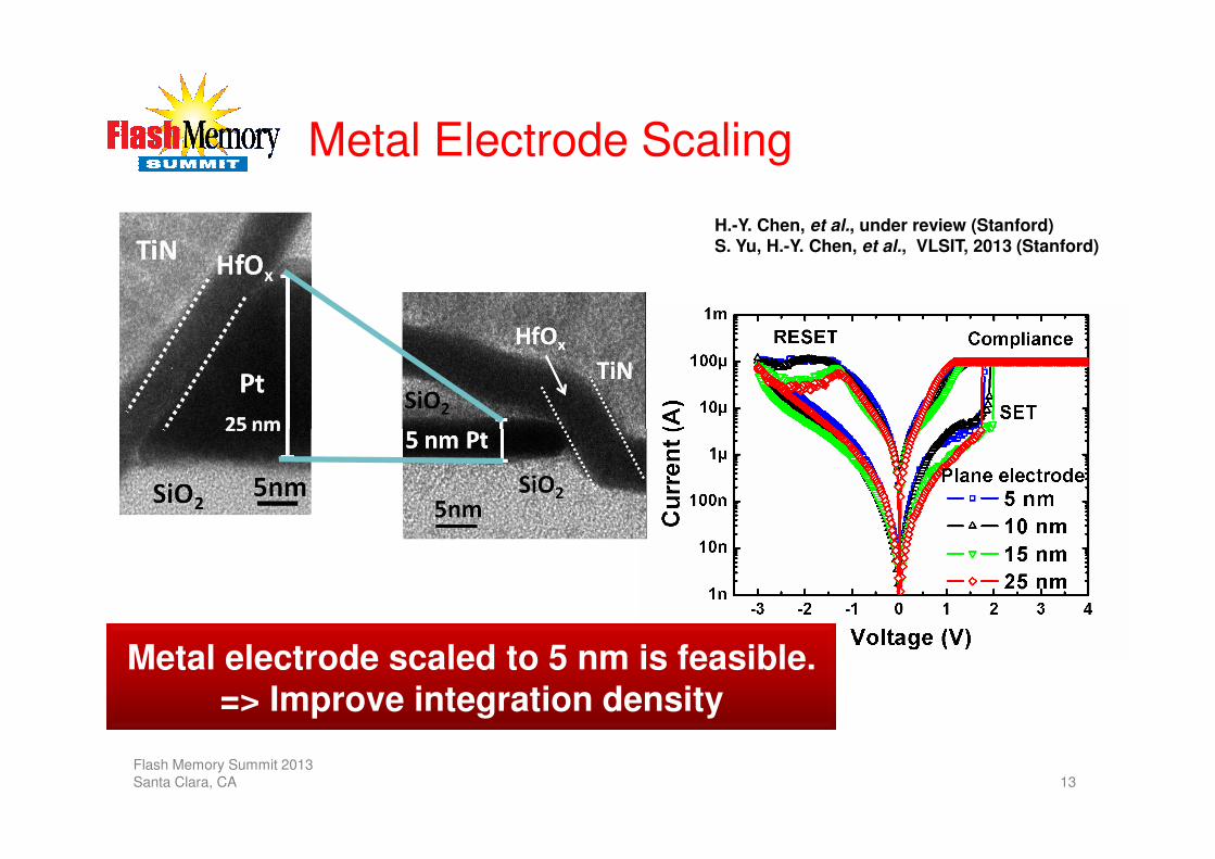
Metal Electrode Scaling
H.-Y. Chen, et al., under review (Stanford)S. Yu, H.-Y. Chen, et al., VLSIT, 2013 (Stanford)
Flash Memory Summit 2013
Santa Clara, CA 13
Metal electrode scaled to 5 nm is feasible.=> Improve integration density

Demonstration of Array Operation
V1 V2 V3 V4
Read D1&D2
0 0 0~1V 0
ReadD3&D4
0 0 0 0~1V
SET D1 0 Float -4V -2V
Flash Memory Summit 2013
Santa Clara, CA 14
RESET D1 0 Float +4V +2V
V/2 write
scheme
S. Yu, H.-Y. Chen, et al.,VLSIT, 2013 (Stanford)

Outline
• 3D Vertical RRAM Demonstration
• Key Issues for 3D Memory Array
• Summary
Flash Memory Summit 2013
Santa Clara, CA 15

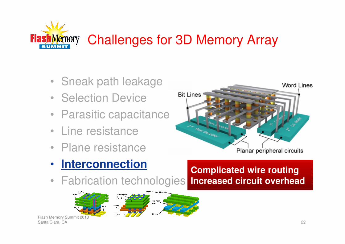
Challenges for 3D Memory Array
• Sneak path leakage
• Selection Device
• Parasitic capacitance
IMEC
VRRAM_1
Stanford
VRRAM_2• Line resistance
• Plane resistance
• Interconnection
• Fabrication technologies
Flash Memory Summit 2013
Santa Clara, CA 16
VRRAM_2
HRRAM
2.5D

Challenges for 3D Memory Array
• Sneak path leakage
• Selection Device
• Parasitic capacitance
Sneak current
• Line resistance
• Plane resistance
• Interconnection
• Fabrication technologies
Flash Memory Summit 2013
Santa Clara, CA 17
Readingcurrent
Sneak path causes read disturbance
problem and increases the power consumption.

Challenges for 3D Memory Array
• Sneak path leakage
• Selection Device
• Parasitic capacitance
Sufficient on/off ratio requirement
High current density requirement Ex. (>10MA/cm2)
Polarity requirement
High endurance requirement• Line resistance
• Plane resistance
• Interconnection
• Fabrication technologies
Flash Memory Summit 2013
Santa Clara, CA 18
High endurance requirement
Scalability requirement
3D low temperature fabrication requirement…

Challenges for 3D Memory Array
• Sneak path leakage
• Selection Device
• Parasitic capacitance
• Line resistance
• Plane resistance
• Interconnection
• Fabrication technologies
Flash Memory Summit 2013
Santa Clara, CA 19
Parasitic capacitance causes RC delay.

Challenges for 3D Memory Array
• Sneak path leakage
• Selection Device
• Parasitic capacitance
• Line resistance
• Plane resistance
• Interconnection
• Fabrication technologies
Flash Memory Summit 2013
Santa Clara, CA 20
~ 4 orders of magnitudes’ increase in Rj at scaled
wire dimensions.
J. Liang, et al. IMW 2012, p. 61.

Challenges for 3D Memory Array
• Sneak path leakage
• Selection Device
• Parasitic capacitance
• Line resistance
• Plane resistance
• Interconnection
• Fabrication technologies
Flash Memory Summit 2013
Santa Clara, CA 21
The thinner the electrode, themore resistive plane electrode=>Higher switching voltages
H.-Y. Chen, et al., under review (Stanford)
Challenges for 3D Memory Array
• Sneak path leakage
• Selection Device
• Parasitic capacitance
• Line resistance
• Plane resistance
• Interconnection
• Fabrication technologies
Flash Memory Summit 2013
Santa Clara, CA 22
Complicated wire routing Increased circuit overhead

Challenges for 3D Memory Array
• Sneak path leakage
• Selection Device
• Parasitic capacitance
• Line resistance
• Plane resistance
• Interconnection
• Fabrication technologies
Flash Memory Summit 2013
Santa Clara, CA 23
Etching capabilityCMOS-friendly material
R. Katsumata, et al. VLSI 2009, p. 136.
Etching AR
~ 30

Challenges for 3D Memory Array
• Sneak path leakage
• Selection Device
• Parasitic capacitance
• Line resistance
• Plane resistance
IMEC
VRRAM_1
Stanford
VRRAM_2• Plane resistance
• Interconnection
• Fabrication technologies
Flash Memory Summit 2013
Santa Clara, CA 24
VRRAM_2
HRRAM
2.5D
All the 3D array designs face thesimilar challenges with the
different degree of influence.
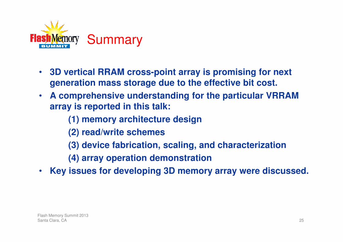
Summary
• 3D vertical RRAM cross-point array is promising for next generation mass storage due to the effective bit cost.
• A comprehensive understanding for the particular VRRAM array is reported in this talk:
(1) memory architecture design(1) memory architecture design
(2) read/write schemes
(3) device fabrication, scaling, and characterization
(4) array operation demonstration
• Key issues for developing 3D memory array were discussed.
Flash Memory Summit 2013
Santa Clara, CA 25

Acknowledgement
Stanford Non-Volatile Memory Technology Research Initiative (NMTRI) member companies
973 Program (2011CBA00602), China
Stanford Nanofabrication Facility (SNF), a member of
Flash Memory Summit 2013
Santa Clara, CA 26
Stanford Nanofabrication Facility (SNF), a member of the NSF-supported National Nanotechnology Infrastructure Network (NNIN)
H.-Y. Chen is additionally supported by
Intel Fellowship
Taiwanese Government Scholarships to Study Abroad
IEEE Electron Devices Society PhD Student Fellowship

Summary
• 3D vertical RRAM cross-point array is promising for next generation mass storage due to the effective bit cost.
• A comprehensive understanding for the particular VRRAM array is reported in this talk:
(1) memory architecture design(1) memory architecture design
(2) read/write schemes
(3) device fabrication, scaling, and characterization
(4) array operation demonstration
• Key issues for developing 3D memory array were discussed.
Flash Memory Summit 2013
Santa Clara, CA 27


![[3DPAM Summit Pittsburgh] 3D Printing and Vertical Integration](https://img.pdfslide.us/doc/110x75/55a9158d1a28ab0d2f8b4624/3dpam-summit-pittsburgh-3d-printing-and-vertical-integration.jpg)