Embed Size (px)
Citation preview

Topical Review
3D printed nanomaterial-based electronic,biomedical, and bioelectronic devices
Samuel Hales1,3, Eric Tokita1,2,3, Rajan Neupane1,3, Udayan Ghosh1,Brian Elder1, Douglas Wirthlin1 and Yong Lin Kong1
1Department of Mechanical Engineering, University of Utah, Salt Lake City, UT 84112, United States ofAmerica2Department of Biomedical Engineering, University of Utah, Salt Lake City, UT 84112, United States ofAmerica
E-mail: [email protected]
Received 1 December 2018, revised 28 October 2019Accepted for publication 5 December 2019Published 6 February 2020
AbstractThe ability to seamlessly integrate functional materials into three-dimensional (3D) constructshas been of significant interest, as it can enable the creation of multifunctional devices. Suchintegration can be achieved with a multiscale, multi-material 3D printing strategy. Thistechnology has enabled the creation of unique devices such as personalized tissue regenerativescaffolds, biomedical implants, 3D electronic devices, and bionic constructs which arechallenging to realize with conventional manufacturing processes. In particular, theincorporation of nanomaterials into 3D printed devices can endow a wide range of constructswith tailorable mechanical, chemical, and electrical functionalities. This review highlights theadvances and unique possibilities in the fabrication of novel electronic, biomedical, andbioelectronic devices that are realized by the synergistic integration of nanomaterials with 3Dprinting technologies.
Keywords: 3D printing, nanomaterials, bioelectronics, biomedical, electronics, additivemanufacturing, multiscale 3D printing
(Some figures may appear in colour only in the online journal)
1. Introduction
The ability of additive manufacturing to seamlessly inter-weave disparate materials into a multifunctional construct canenable the creation of unique biomedical and electronicdevices. Additive manufacturing, also known as ‘3D print-ing’, is defined by the American Society for Testing andMaterials (ASTM) as ‘a process of joining materials to makeobjects from 3D model data, usually layer upon layer [1].’Traditionally developed as a rapid prototyping technique, 3Dprinting has become increasingly accessible with the adventof low-cost desktop 3D printers [2, 3], and increasinglypowerful with the development of novel printing technologies
[4–9]. 3D printing has been heralded for its capability tocreate geometrically complex constructs with low cost andminimal material waste and has been increasingly utilized bythe aerospace and automotive industries—particularly forhighly customized, low-volume production where the econ-omy of scale of conventional mass production is no longerapplicable [10, 11].
3D printing is also projected to have a significant impactbeyond these industries, especially in the field of medicineand personalized electronics. For example, it can address awide range of unmet clinical needs [12, 13] with the creationof personalized implants [14], regenerative scaffolds [15, 16],and drug delivery devices [17, 18]. Furthermore, 3D printedmodels of patients’ unique anatomy, acquired with modernmedical imaging technologies, can improve surgery planning,
Nanotechnology
Nanotechnology 31 (2020) 172001 (40pp) https://doi.org/10.1088/1361-6528/ab5f29
3 Equal contribution.
0957-4484/20/172001+40$33.00 © 2020 IOP Publishing Ltd Printed in the UK1

implant design, and provide unprecedented medical training[19, 20]. In another exciting development, the 3D printing ofliving cells could lead to the creation of biological constructsthat can regenerate or augment lost tissues or organs due todiseases, trauma or congenital disabilities [16, 21]. In the fieldof electronics, 3D printing can enable the creation of non-planar [22], flexible [23], wearable [24], and—more recently—ingestible gastric resident electronics [18, 25].
Nanomaterials are materials with one dimension between1 and 100 nm. The addition of nanomaterials to 3D printedconstructs can impart functional properties such as electrical[26], magnetic [27], and optical properties [22]. Importantly,at the nanometer scale, a subset of functional materials exhibitsize-dependent properties; this allows for the fine-tuning ofthe properties by synthesizing different sizes of the nanoma-terials. For example, the size dependence of the emissionwavelength [22] of quantum dots (semiconducting nano-particles) can be leveraged to create a display device withexceptionally high color purity [28]. Furthermore, a materialwith dimensions on this scale exhibits significant changes toits surface-to-volume ratio, allowing the fine-tuning of phy-sical and chemical properties such as a lower melting point,higher chemical reactivity, and higher surface conductivity incomparison to the same material in its bulk form [29].
The synergistic integration of nanomaterials with a multi-material additive manufacturing approach can extend thereach of 3D printing technologies beyond the creation ofpassive single-material constructs [7]. The ability to seam-lessly integrate functional nanomaterials with distinct mate-rials is a compelling fabrication approach that enables thecreation of freeform architectures such as three-dimensional(3D) composite structures [30–33] and multi-functional con-structs with unprecedented performance and unique proper-ties. In particular, the application of 3D printing in thecreation of biomedical and electronic devices is especiallyattractive [34, 35] due to the inherent heterogeneity of com-plex biological systems and the potential to overcome planarconstraints of microfabricated electronic systems [7, 12]. Thefield of bioelectronics, a subset of biomedical, has especiallynotable applications due to the ability of 3D printing toseamlessly interweave electrically conductive nanomaterialsinto geometrically complex, biocompatible scaffolds anddevices that replicate the inherent complexity and flexibilityof biological systems [36–38]. Indeed, conventional sub-tractive manufacturing methods—such as machining, drilling,grinding, and lithographic processes—or formative manu-facturing methods, such as forging and investment casting,are inherently limited in their ability to create complex geo-metries and/or multifunctional, multi-material structures [11].
This review highlights the advances in the developmentof unique electronic, biomedical, and bioelectronic functionaldevices that leverage the synergistic integration of additivemanufacturing with nanomaterials. We will first introducecommonly used 3D printing approaches and the ability ofnanomaterials to impart functional properties. We will thenhighlight the development of 3D printed nanomaterial-basedelectronics, such as energy storage devices (figure 1(A)) andphotonic devices (figure 1(B)), and discuss how these enable
the creation of flexible and wearable sensors (figure 1(C)) thatcan overcome the limitations of conventionally fabricatedelectronics. Next, we will review the creation of uniquenanomaterial-based, 3D printed biomedical devices. These arediscussed in relation to the customization of mechanical(figure 1(D)), geometric (figure 1(E)), biological (figure 1(F)),
Figure 1. The synergistic integration of 3D printing with a widerange of materials enables the creation of unique electronic,biomedical, and bioelectronic functional devices. For example,electronics such as (A) interdigitated electrodes for use in a lithium-ion microbattery can be 3D printed with lithium titanate (Li4Ti5O12,LTO) and lithium iron phosphate nanoparticles (LiFePO4, LFP). [39]John Wiley & Sons. Copyright © 2013 WILEY‐VCH Verlag GmbH& Co. KGaA, Weinheim. (B) A multicolor display can be printedwith perovskite lead halide nanocrystals. [40] John Wiley & Sons.© 2019 WILEY‐VCH Verlag GmbH & Co. KGaA, Weinheim.(C) A flexible electronic device can be 3D printed with reducedgraphene oxide (rGO). Reprinted from [23], Copyright (2016), withpermission from Elsevier. In biomedical devices, (D) hexagonalboron nitride (hBN) imparts increased mechanical flexibility to a 3Dprinted poly(lactic-co-glycolic acid) (PLGA) sheet. Reprinted withpermission from [41]. Copyright (2018) American ChemicalSociety. Similarly, (E) thick vascularized tissue can be 3D printed, asshown by a biological construct immersed in a support bathmimicking a small-scale heart. Reproduced from [42]. CC BY 4.0.(F) 3D printed calvarial bone with microchannels can be fabricatedusing polycaprolactone (PCL) doped with tricalcium phosphate(TCP) nanoparticles to facilitate vascularization. Reprinted bypermission from Springer Nature Customer Service Centre GmbH:Springer Nature, Nature Biotechnology, [43], 2016. In bioelectronicdevices, (G) flexible microelectrode arrays can be 3D printed withsilver nanoparticles on complex substrates such as gelatin andattached to a circuit board for action potential measurements of cellculture. Reproduced from [44]. CC BY 4.0. (H) A 3D printed bionicear containing gold nanoparticle-infused silicone and cultured livingcells (chondrocytes) demonstrates improved audio sensing over ahuman ear. Reprinted with permission from [45]. Copyright (2013)American Chemical Society. (I) Soft strain gauges printed withcarbon nanoparticle ink guide the regeneration and measure thebeating strength of cardiac tissue. Reprinted by permission fromSpringer Nature Customer Service Centre GmbH: Springer Nature,Nature Materials, [46], 2016.
2
Nanotechnology 31 (2020) 172001 Topical Review

and responsive properties, and include personalized regen-erative constructs, biological implants, and drug deliverymethods which possess unique properties that are endowed bynanomaterials. Finally, we will highlight the merging ofbiological constructs and electronics enabled by this multi-scale 3D printing approach. The bioelectronic devicesreviewed include microelectrodes (figure 1(G)), the interfa-cing point between biological electricity and fabricated elec-tronics; bioelectronic scaffolds (figure 1(H)), which useelectricity to potentially enhance cell regrowth and recovery;biosensors, which measure an array of biological organismsand molecules; and lab-on-a-chip devices (figure 1(I)), whichenable the systematic study of complex biological processes.
2. 3D printing methods
3D printing, as previously described, is defined by the ASTMas ‘a process of joining materials to make objects from 3Dmodel data, usually layer upon layer [1].’ 3D printed struc-tures are first digitally constructed as 3D models withcomputer-aided design (CAD) software and converted into adigital approximation of the model such as a stereo-lithography (STL) file. This geometry is then interpreted andsynthesized into machine code which the 3D printer uses tosolidify regions of resins, powders, or inks layer by layer intoa 3D construct [47]. 3D printing is a broad class of manu-facturing technologies, which Lewis et al [6] categorized aslight and ink-based. In this review, we will describe keytechnologies that can potentially be integrated with nanoma-terials for the creation of functional devices.
2.1. Light-based methods
Light-based 3D printing methods use light to selectivelysolidify photocurable resins or sinter polymer, ceramic, ormetal powders. For example, stereolithography (SLA), shownin figure 2(A), was one of the first 3D printing methods tested[48] and has a minimum feature size of down to 50 μm [49].It uses a basin of photocurable resin which is selectivelyphotopolymerized by ultraviolet (UV) laser one volume ele-ment (voxel) at a time. Once a layer of resin is fully solidifiedon the build platform, the platform retracts and a new layer ofresin is introduced. Digital projection lithography (DLP)[50, 51] and continuous liquid interface production (CLIP) [4]also precisely solidify photocurable resin, but are able tosolidify an entire layer of resin at a time—increasing printspeeds to 6×10⁻² ml h−1. DLP accomplishes this by using adigital micromirror device [50] or a liquid crystal display [51]as a dynamic mask and projecting the mask pattern on theliquid resin, as shown in figure 2(B). CLIP further acceleratesthe process with an oxygen-permeable build window whichenables a thin (∼10 μm) layer of uncured, oxygen-containingresin to exist between the window and the part. UV imagescan thus be continuously projected through the window, andthe part can be steadily drawn out of the resin in minutes [4].A representation of CLIP is shown in figure 2(C). Two-photon polymerization 3D printing (2PP) is another light-
based method where ultrashort IR (infrared) laser pulses areused to polymerize a tiny voxel within the reservoir of liquidresin [4]. This enables an exceptional 100 nm feature sizewithout the need for a retractable platform. Further, the totalpart size can reach approximately 1 cm3 [6]. In general, theprinting materials of SLA-based techniques are limited tophotocurable resins. Post-processing is also required—including post-curing with UV light and the removal of thesupports generated during the printing process [49].
In selective laser sintering (SLS), instead of a photocur-able resin, a bed of polymer, ceramic, or metal powder issintered with a laser on a retractable bed [55, 56]. When alayer is completely sintered, the bed retracts into the powderand a fresh layer of powder is rolled onto the top of the part,as shown in figure 2(D). The powder bed supports the con-struct, hence no additional supporting structures need to begenerated during the printing process. This method is limitedby the size of the particles to be sintered, but can still achievea feature size of approximately 100 μm [6]. Generally, thefinal parts are highly porous, and the thermal stresses from thehigh-temperature laser have to be considered as they cancause distortion to the printed part [56].
2.2. Ink-based methods
Ink-based 3D printing methods use inks or thermoplasticfilaments which are extruded through a nozzle and selectivelydeposited onto a substrate [6, 7]. Ink-based 3D printing can besubcategorized into filament and droplet-based methods.Filament-based methods continuously extrude an ink orthermoplastic filament onto a build plate, while droplet-basedmethods deposit low-viscosity fluids (2–102 MPa s) [12, 57].
In fused deposition modeling (FDM) motors drivethermoplastic filament through a heated nozzle. The meltedfilament is selectively deposited onto a build plate, where itagain solidifies—as shown in figure 2(E). Due to its relativesimplicity, FDM filaments and printers can be inexpensive(printers cost as little as $200). Further, multiple heated nozzlescan be integrated to achieve multi-material prints [58].Post-processing is required to remove supports for complexstructures, however, and filaments must be preformed forextrusion. Direct ink writing (DIW), another class of filament-based 3D printing, uses pneumatic pressure, a piston, or screwto extrude liquid ink through a nozzle (as shown in figure 2(F)).In some DIW, post-processing steps are used solidify theextruded ink, such as photopolymerization or thermal curing[6]. Inks can be formulated from polymeric and colloidalsuspensions [59], and because no high temperatures areinvolved in the printing process, bioprinting (the printing ofliving cells) is also possible [21, 60–62].
Electrospinning is another filament-based 3D printingmethod, which can generate nanoscale fibers. In electrospin-ning, a high voltage is first applied between a nozzle con-taining the ink and the grounded collector. When theelectrostatic repulsion within the ink becomes more sig-nificant than the surface tension at the head of the nozzle, acharged jet of liquid ejects from the nozzle towards thegrounded substrate, as shown in figure 2(G). While far-field
3
Nanotechnology 31 (2020) 172001 Topical Review

electrospinning (where the distance between the needle andthe substrate is typically between 5 and 15 cm) forms dis-ordered mats of nanoscale fibers that can be under 100 nmwide, near-field electrospinning (500 μm–5 cm) allows forcontrolled deposition of micrometer-wide fibers [63, 64].Organic polymers are most commonly used in electrospin-ning, but small molecules, colloidal particles, and compositeshave been utilized as well [63, 65, 66].
Aerosol jet printing (AJP), as shown in figure 2(H), isalso a filament-based 3D printing method. In AJP, an ink isfirst converted into an aerosol using an ultrasonic or pneu-matic atomizer, then combined with a carrier gas for trans-portation, and finally compressed into a focused stream by a
sheath gas just before ejection [67]. The use of a powerfulaerosol stream allows this technique to print in multipledirections, including upwards, and on complex surfaces, suchas on five orthogonal sides of a cube [68]. Commercial AJPsystems can generate aerosol using inks with viscosities from1 to 1000 cp, allowing a wide range of usable materials—from metals [69], ceramics [70] and polymers to biologicalmatter [71]—to be printed at high resolution (10 μm).
Direct inkjet printing is a droplet-based 3D printingmethod which primarily uses piezoelectric or thermal nozzlesto propel low-viscosity fluids onto a build plate [72, 73].Thermal printers heat the ink for a few microseconds so thatan expanding bubble forces a drop of ink through the nozzle,
Figure 2. Representations of light and ink-based 3D printing methods. Light-based methods include (A) stereolithography (SLA), (B) digitalprojection lithography (DLP), (C) continuous light interface projection (CLIP), and (D) selective laser sintering (SLS). Ink-based methodsinclude (E) fused deposition modeling (FDM), (F) direct ink writing (DIW), (G) electrospinning, (H) aerosol jet printing (AJP), and (I) directinkjet printing. (A and E) Reprinted from [52], Copyright (2016), with permission from Elsevier. (B) [53] John Wiley & Sons. © 2018WILEY‐VCH Verlag GmbH & Co. KGaA, Weinheim. (C, D and F) Reprinted by permission from Springer Nature Customer Service CentreGmbH: Springer Nature, Nature, [6], 2016. (H) Reprinted with permission from [54]. Copyright (2013) American Chemical Society. (I) [12]John Wiley & Sons. © 2018 WILEY‐VCH Verlag GmbH & Co. KGaA, Weinheim.
4
Nanotechnology 31 (2020) 172001 Topical Review

while piezoelectric printers apply voltage to a glass tube orbending plate which then propels a droplet through thenozzle [74]. Often the resin is then UV cured, as shown infigure 2(I). Ink droplets as small as 2–12 pl can be depositedwith this method [75], and multiple nozzles can be usedsimultaneously for multi-material printing [76]. Similar toDIW and AJP, the deposition of ink without high tempera-tures allows for the deposition of a wide range of polymers[77], suspensions [78], and living materials [79, 80].However, the viscosity is limited to less than 0.25 Pa s, andthe ink has to be precisely formulated to prevent nozzleclogging [81]. Using inkjet printing to actuate binding agents,binder jet 3D printing creates 3D structures by bindingpolymer, metal, or ceramic powder [56]. The use of binder onpowder prevents the thermal stresses that can occur after SLSprinting, but often requires steps such as sintering or infil-tration (addition of strengthening materials) after binding toimprove mechanical strength [82].
Electrohydrodynamic jet (e-jet) printing uses a similarsetup as electrospinning, with a voltage applied between anink-filled nozzle and a grounded substrate; applying thisvoltage creates an electrostatic charge in the ink that canovercome the surface tension of the liquid. Instead of ejectingcontinuous fibers, e-jet printing uses a pulsed voltage to ejectdroplets that can be as small as attoliters in volume, and printspots that are under 100 nm in diameter [83–85]. The mate-rials used in e-jet printing are comparable to those used inelectrospinning, including organic polymers, colloidal parti-cles, and composites [84].
3D printer resolution can be divided into three sub-categories: Z resolution, XY resolution, and minimum featuresize [86]. Z resolution corresponds to the minimum allowablelayer height in a printing method. In techniques such as SLAor FDM, this value is reported as the resolution of the motorsdriving the height of the build plate or printer nozzle. Incontrast, for methods such as direct inkjet printing, the dropletthickness determines the Z resolution. Similarly, XY resolu-tion corresponds to the minimum allowable horizontalmovement of the build plate, nozzles, or optics. While XYresolution is determined by the motion of the printer, mini-mum feature size can be defined as the smallest horizontalfeature that can feasibly be created in a printing method. Inlight-based 3D printing methods, this value is primarilydetermined by the beam size of the photocuring or sinteringlight. For SLA, the minimum feature size is determined by thespot size of the laser [87] and in DLP and CLIP it is based onthe pixel size [53]. In SLS, this depends on both the laser spotsize and the size of the particles to be sintered [6]. In filament-based 3D printing methods, feature size is determined by thediameter of the nozzle or fiber [6]. In droplet-based methodssuch as direct inkjet and e-jet printing, the footprint of an inkdroplet determines feature size [88], and binder jet feature sizeis determined by both the footprint size and the particle dia-meters [89]. For more information regarding 3D printingtechnologies and applications, the reader is referred to severalexcellent reviews [3, 6, 12, 34, 90, 91]. Table 1 also providesa brief overview of 3D printing technologies.
3. Properties of nanomaterials
Nanomaterials are materials with one dimension of ca. 1–100nm, and their proximity to the scale of atoms and molecules(the diameter of a DNA strand being approximately 2 nm[102]) results in properties that differ from the same materialin its bulk form [103]. A material in its bulk form generallyhas well-defined properties, such as melting temperature,chemical reactivity, and color. Gold in its bulk form has amelting temperature of 1064 °C, is not a catalyst, and has acharacteristic yellow color. In contrast, gold nanoparticleshave a melting temperature of approximately 300 °C–400 °C,effectively catalyze specific reactions, and appear red topurple [104]. Indeed, a subset of material properties, such asmelting point and emission spectra, can be modulated bychanging the size of the particles, which enable the tuning ofmaterial properties by changing the size of the materials.
First, approaching the nanometer scale, the significantlyincreased surface-to-volume ratio of nanomaterials comparedto that of their bulk form has an important geometrical effect[29]. For example, the greater relative number of weaklybound atoms at the surface increases the chemical reactivityof nanomaterials and allows some to be used as catalysts.Nanomaterial catalysts can be recycled multiple times (someup to 20 [105–107]) without loss of activity, and their smallsize allows many reactions to occur simultaneously[108, 109]. The weakly bound surface atoms in nanomaterialsalso result in melting-point depression due to their reducedcohesive energy. Similarly, conductive nanomaterial tracescan be sintered at lower temperatures than the same materialin bulk [110]. The increased surface area of metal nanoma-terials has allowed for the creation of novel devices, such asmicro-supercapacitors which can fully charge and dischargein seconds and operate for millions of cycles without losingenergy storage capacity [111]. Ion access to supercapacitorelectrodes is increased with the use of nanoparticle electrodes,allowing for a greater amount of charge to be transferred.
Second, a subset of nanomaterial properties begins to besize-dependent as they approach the nanometer scale. Thissize-dependency can be leveraged to fine-tune or to achieveprecise properties of interest by varying the particle size. Forexample, for semiconducting nanomaterials, the quantumconfinement effect results in the modulation of energy levelsas the motion of their electrons are confined in a higher degreethan their corresponding bulk counterpart [112]. Some effectsof quantum confinement include the optical absorption ofshorter wavelengths—such as the color shift of gold nano-particles mentioned above—and a shift in emission wave-length of quantum dots. The extent of this absorption andemission shift depends on the size of the nanomaterials,allowing for the creation of quantum dot light-emitting diodes(LEDs) with various emission spectra by varying the size ofthe nanomaterials used [113, 114]. The plasmon resonance ofnanomaterials is tunable as well. Plasmon resonance is theoscillation of free electrons at the surface of metals driven bythe absorption of electromagnetic waves, an oscillation ana-logous to a simple mass-spring-damper oscillator model[115]. The electron cloud at the surface of a metal oscillates
5
Nanotechnology 31 (2020) 172001 Topical Review
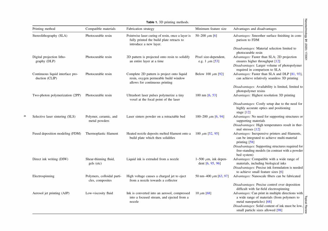
Table 1. 3D printing methods.
Printing method Compatible materials Fabrication strategy Minimum feature size Advantages and disadvantages
Stereolithography (SLA) Photocurable resin Pointwise laser curing of resin, once a layer isfully printed the build plate retracts tointroduce a new layer.
50–200 μm [6] Advantages: Smoother surface finishing in com-parison to FDM
Disadvantages: Material selection limited tophotocurable resin
Digital projection litho-graphy (DLP)
Photocurable resin 2D pattern is projected onto resin to solidifyan entire layer at a time
Pixel size-dependent,e.g. 1 μm [53]
Advantages: Faster than SLA; 2D projectionensures higher throughput [12]
Disadvantages: Larger volume of photopolymerrequired in comparison to SLA
Continuous liquid interface pro-duction (CLIP)
Photocurable resin Complete 2D pattern is project onto liquidresin, oxygen permeable build windowallows for continuous printing
Below 100 μm [92] Advantages: Faster than SLA and DLP [81, 93],can achieve relatively seamless 3D printing
Disadvantages: Availability is limited, limited tophotopolymer resins
Two-photon polymerization (2PP) Photocurable resin Ultrashort laser pulses polymerize a tinyvoxel at the focal point of the laser
100 nm [6, 53] Advantages: Highest resolution 3D printing
Disadvantages: Costly setup due to the need forhighly accurate optics and positioningstage [12]
Selective laser sintering (SLS) Polymer, ceramic, andmetal powders
Laser sinters powder on a retractable bed 100–200 μm [6, 94] Advantages: No need for supporting structures orsupporting materials
Disadvantages: High temperatures result in ther-mal stresses [12]
Fused deposition modeling (FDM) Thermoplastic filament Heated nozzle deposits melted filament onto abuild plate which then solidifies
100 μm [52, 95] Advantages: Inexpensive printers and filaments,can be integrated to achieve multi-materialprinting [58]
Disadvantages: Supporting structures required forfree-standing models (in contrast with a powderbed system)
Direct ink writing (DIW) Shear-thinning fluid,gels (etc)
Liquid ink is extruded from a nozzle 1–500 μm, ink depen-dent [6, 95, 96]
Advantages: Compatible with a wide range ofmaterials, including biological inks
Disadvantages: Precise ink formulation is neededto achieve small feature sizes [6]
Electrospinning Polymers, colloidal parti-cles, composites
High voltage causes a charged jet to ejectfrom a nozzle towards a collector
50 nm–400 μm [63, 97] Advantages: Nanoscale fibers can be fabricated
Disadvantages: Precise control over depositiondifficult with far-field electrospinning
Aerosol jet printing (AJP) Low-viscosity fluid Ink is converted into an aerosol, compressedinto a focused stream, and ejected from anozzle
10 μm [68] Advantages: Can print in multiple directions witha wide range of materials (from polymers tometal nanoparticles) [68]
Disadvantages: Solid content of ink must be low,small particle sizes allowed [98]
6
Nanotechnology
31(2020)
172001TopicalR
eview

Table 1. (Continued.)
Printing method Compatible materials Fabrication strategy Minimum feature size Advantages and disadvantages
Direct inkjet printing Low-viscosity fluid Thermal or piezoelectric nozzles propel inkdroplets onto a build plate
10–100 μm [6, 99] Advantages: Multi-material printing possible,high resolution, compatible with biological inks
Disadvantages: Printing resolution is highlydependent on ink formulation and nozzle size
Binder jet printing Polymer powder andliquid binder
Droplets of binder are ink-jetted onto a pow-der bed
170 μm [95] Advantages: No thermal stresses in the finishedpart (in contrast with SLS)
Disadvantages: Mechanical properties inhibitedby porosity, often post-processing required [82]
Electrohydrodynamic jet (e-jet)printing
Polymers, colloidal parti-cles, composites
High voltage causes a charged droplet to ejectfrom a nozzle towards a collector
240 nm–50 μm [100] Advantages: Higher resolution in comparison toDIW and SLA
Disadvantages: Requires carefully manufacturednozzles and precise voltages [101]
7
Nanotechnology
31(2020)
172001TopicalR
eview

like a dipole parallel to the direction of the electric field in thedriving electromagnetic waves. The resonant frequency ofthis oscillation in nanomaterials is determined by the size ofthe particles, thus allowing for tunable control [116]. Nano-particles can absorb wavelengths that are larger than theparticles themselves, and the enhanced electromagnetic fieldnear the particle surface has several exciting applications. Forinstance, it enables the creation of highly sensitive biosensors[116–118], enables active targeting of nanoparticles to cancercells [119], and improved solar cell efficiency [120, 121].
In another example, the magnetic domains and con-ductivity of nanomaterials are also influenced by their size.Magnetic nanomaterials on the range of 10–20 nm are com-prised of a single magnetic domain and can exhibit super-paramagnetism, where the magnetic field randomly switchesdirection under the influence of heat [122]. The ability todirect or extract magnetic nanomaterials in solution with amagnetic field has also spawned their potential use as retrie-vable biosensors, enzymes, and catalysts [117].
Due to the inherent porosity that is introduced in a sig-nificant subset of 3D printing methods (such as SLS), nano-materials have also been utilized to enhance the mechanicalproperties of printed parts—providing increased tensilestrength, for example [123]. The inclusion of nanomaterialsinto 3D printing processes results in devices with significantlymodified material properties, tunable photonic effects [22],electrical conductivity [26], and magnetic properties [27].Table 2 describes examples of nanomaterial integration in themodulation of the material properties of 3D printed parts.SLA and DLP are grouped in table 2 as the introduction ofnanomaterials into the photocurable resins of these light-based 3D printing methods will similarly affect the propertiesof the finished products [124]. Additionally, the authors arenot aware of achieved nanomaterial integration with CLIPdue to its relatively recent development [125]. To the best ofour knowledge, the company owning this patented technol-ogy does not currently offer nanomaterial resins and printersare normally available by subscription [126].
4. 3D printed devices with nanomaterials
4.1. Electronics
Printed electronics is a rapidly evolving field whereinprinting technologies are applied to fabricate electronic cir-cuits and devices [173]. Conventionally, electronic devicesare manufactured on rigid substrates by planar processessuch as photolithography [174], electroless plating[175, 176], or vacuum deposition [177, 178]. Fundamen-tally, these processes suffer from two shortcomings. First,subtractive fabrication methods are generally planar in nat-ure, which often impedes the fabrication of enclosed geo-metries, voids, overhangs, or 3D structures. Second, most ofthese traditional methods are limited to the processing of asingle material per processing step. This limits their abilityto produce electronics with multifunctional properties.
On the other hand, the 3D printing of nanomaterials allowsfor the customization of device geometry and enables themulti-material, multiscale fabrication of electronic devices. Theability to incorporate nanomaterials in an electronic printingsystem can impart properties such as electrical conductivity[173] and optical properties [165, 179, 180]. High-performanceenergy storage devices such as lithium-ion batteries [181] andmicrosupercapacitors [182], flexible electronics [183] as wellas photonic devices [184] have been developed by leveragingthe functional properties of nanomaterials integrated with var-ious light-based and ink-based methods.
4.1.1. Energy storage devices. A key prerequisite for theadvancement of flexible and wearable devices is thedevelopment of high performance energy storage micro-devices with high energy density and fast charging/discharging rates [39]. Energy storage devices typicallyretain energy based on the electrochemical reaction thattypically occurs between two different electrodes: the anodeand cathode. Nanomaterials such as graphene, grapheneoxides, silver, and carbon nanotubes have been used in thefabrication of the electrodes and electrolytes of energystorage devices [185–187]. Recent development in 3Dprinting technologies have enabled the creation of 3Dprinted nanomaterial-based energy devices such as lithium-ion (Li-ion) batteries [39], microsupercapacitors [188], andpseudocapacitors [182].
The ability of additive manufacturing to print multiplematerials simultaneously could reduce the number ofprocessing steps required to fabricate energy storage devices.Unlike traditional subtractive methods which are often limitedto handling a single material at a time, 3D printing allows theincorporation of multiple functional nanomaterials. Moreover,the assembly of nanomaterials with other components in anelectrochemical device could be optimized to ensure that theunique properties of the nanomaterials, such as high surfacearea and electrical conductivity, are not compromised. Rochaet al [189] used a single-step DIW method with post-processing to fabricate electrodes for supercapacitors andbatteries. They prepared thermo-responsive inks—inks whoseproperties are dependent on their temperature—to fabricatethe electrodes. The electrodes consisted of chemicallyreduced graphene as the active material and copper as thecurrent collecting material. The thermal reduction of thegraphene-based ink and sintering conditions of copper (i.e.sintering temperature) match well so that the reduction andsintering could occur simultaneously. By using this strategy,they were able to preserve the electrical properties of thegraphene ink. Figure 3(A), left shows the fabricated double-legged and single-legged electrodes assembled to create asupercapacitor, and the enhanced image shows its compo-nents. Figure 3(A), right is a scanning electron microscopy(SEM) image of the interface region between the graphene-based ink and the copper collector illustrating good physicalcontact, which results in enhanced performance of the device.Hence 3D printing offers the flexibility to print bespoke inksconsisting of multiple materials in a single printing step,
8
Nanotechnology 31 (2020) 172001 Topical Review

Table 2. 3D printed nanomaterials: the effects of the addition of nanomaterials on the material properties of 3D printed constructs and on therespective printing process. Properties discussed include modulus of elasticity (E), strain to failure (ε), ultimate tensile strength (UTS),compressive strength (CS), flexural strength (FS), stiffness (k), and shear stress (τ).
3D printing method Carbon-based Metals Ceramics/others
Stereolithography(SLA) and
Graphene: increased UTS andductility [127]
Silver NPs: increased UTS, E, andglass transition temperature;decreased ε [128, 129]
Silica: increased UTS, E, and ε,printing accuracy not affected[130, 131]
Digital projection litho-graphy (DLP)
CNT: increased UTS, lower maxε [132] Gold NPs: increased thermal stabi-
lity and k (up to 0.16 μMgold) [133]
Attapulgite (ATP): increased TSand E, printing accuracy sig-nificantly reduced [131]
Iron NPs: increased CS and E,decreased ε when combined withpoly(ethylene glycol) diacrylate(PEGDA) [134]
Montmorillonite: increased UTSand E, printing accuracy sig-nificantly reduced [131]
Hydroxyapatite (nHa): compar-able CS, increased E [135]
Two-photon polymeriza-tion (2PP)
CNT: spontaneous alignment ofCNT observed along nanowireaxis which could potentiallyresult in programmable aniso-tropic properties [136]
Gold NRs: increased storage mod-ulus and hardness [137]
CdSe-ZnS: fluorescent [138]
Titanium dioxide NPs: tunablerefractive index, high concentra-tions of nanoparticles made poly-merization difficult [139, 140]
Magnetite NPs: superparamagneticactuation abilities [141]
Selective laser sinter-ing (SLS)
MWCNT: increased UTS and E,decreased ε, greater fatiguestrength [142]
Silver NPs: resistivity (3.0×10⁻⁵
Ω cm) close to that of bulk(1.59×10⁻⁶ Ω cm), significantheat-affected zone [143]
Calcium phosphate: slightlyincreased CS (from ∼0.48 to∼0.57 MPa for nanocompositescaffolds, compared to purepolymer scaffolds in dry con-ditions), biocompatible [144]
Copper NPs: resistivity less than 3×that of bulk copper (depending onthe laser irradiance levels) withminimal oxidation [145]
Iron NPs: decreased creep andshrinkage [123, 146]
Fused deposition model-ing (FDM)
Graphene: increased E (0–8 wt%graphene), decreased UTS andε, excessive wear on printnozzles [147, 148]
Iron NPs: increased compressionmodulus, decreased CS and com-parable max ε [134]
Silica: increased UTS, FS, maxε, improved heat flow andisotropy of part [149]
CNTs and Carbon nanofibers:increased UTS, E, and k;decreased ε compared to virginpolymer matrix, excessive wearon print nozzles [148, 150, 151]
Montmorillonite: increased UTS,E, FS; decreased thermalexpansion coefficient and maxε [149, 152]
Calcium carbonate: increasedUTS, FS, ε, improved heatflow and isotropy of part [149]
Direct ink writing (DIW) Graphene: increased E (0%–20%graphene), increased ε (>210%for 20% graphene), increasedconductivity (∼600 S m−1 at40% particle loading) [153]
Silver NPs: maintained conductivityover many loading cycles [154]
CdSe-ZnS: fluorescent [22]
CNT: increased CS to ∼9 MPacompared to ∼4 MPa forpolymers without CNT [155]
Iron NPs: increased E (83 MPa) incomparison to divalent cations (17MPa), imparts magnetic proper-ties [156]
Electrospinning Graphene: controllable swelling,no negative effects on thenanofibers’ morphology [157]
Gold NRs: act as a photothermalagent, biocompatible [158],increased storage modulus (at 1, 2,and 3 wt% gold) [137]CNT: biocompatible, increased
cell alignment, decreased cel-lular attachment [159]
9
Nanotechnology 31 (2020) 172001 Topical Review

which could reduce the fabrication time of energy storagedevices. Additionally, Kim et al utilized novel materialcombinations to develop a fully-3D printed aqueous zinc-ionbattery [190]. Their studies used polyaniline-coated carbonfiber cathodes, zinc anodes and an SLA-printed porousseparator to fabricate rechargeable batteries. The SLA printerconstructed different battery geometries with variable charge-discharge curves, highlighting an advantage of 3D printed,electronic devices.
Extrusion-based 3D printing allows for the fabricationof energy storage device components with hierarchicalgeometries that could facilitate rapid ion transport in theinterface between electrode and electrolyte, ultimatelyenhancing the charging/discharging rate [193, 194]. Hier-archy in a geometrical context refers to the presence oftypical feature sizes that span across orders of magnitude. Astructure possessing pore sizes that range from the nanoscaleto the macroscale is said to have a hierarchical structure. Inprinted electronics, devices having components that exhibithierarchical dimensions typically display enhanced perfor-mance compared to those with stochastic feature sizes. The
presence of a hierarchy in pore sizes in an electrode of anelectrochemical storage device could enhance chargetransfer and diffusion of ions [195]. For example, holeygraphene oxide, a nanoporous graphene-based material, wasused to synthesize printable ink for the electrodes of abattery [191]. Figure 3(B), left shows the preparationof holey-graphene ink. Pore sizes from a few nanometers(4–25 nm through holes) to hundreds of micrometers(<500 μm square pores) were obtained in the printable ink.Figure 3(B), right shows the deep discharge curve of theprinted parts with porous and nonporous features. Theporous electrode of the holey graphene shows an increasedareal capacitance (∼13 mAh cm−2) in comparison to theparts made up of graphene oxides such as Vor-X graphene(∼10 mAh cm−2) and natural graphite (∼3 mAh cm−2).Recently, Zhu et al fabricated supercapacitors based onhierarchical graphene aerogels with periodic macropores byusing DIW [193]. These macropores facilitate mass trans-port, ultimately enabling the fabrication of supercapacitorswith superior rate capability (ca. 90% from 0.5 to 10 A g–1)compared to the other carbon-based electrodes [196]. In a
Table 2. (Continued.)
3D printing method Carbon-based Metals Ceramics/others
Aerosol jet printing (AJP) Graphene: maintained con-ductivity over 1000 bendingcycles [160]
Silver NPs: maintained conductivityover 1000 bending cycles,enhanced conductivity with addi-tion of CNTs [160, 161]CNT: adjustable conductivity
(conductivity of compositeincreases from insulating toconductive at 1.64 wt% to 3.22wt% of CNTs) [162]
Direct inkjet printing Graphene: annealing improvesconductivity of graphene/nitrocellulose films (to∼40 000 S m−1), negligiblechange in resistance over 2000bending cycles [163]
Silver NPs: reduced shrinkage anddistortion, maintained mechanicalstability over 1000 bendingcycles [164]
CsPbBr3 NCs: fluorescent [165]
CNT: average carrier mobility of4 cm2 V−1 s−1 and ON/OFFcurrent ratios of 104 in thin filmtransistors [166]
Gold NPs: sintering improves con-ductivity, stable resistance over1000 bending cycles [110]
Binder jet printing Copper: increased green strengthand density, decreased shrinkage,increased porosity and somefoaming observed at high con-centrations (20%–40% vol.)[167, 168]
Alumina: increased CS and den-sity (from 76 to 641 kPa for0%–15% Alumina), decreasedporosity [169]
Electrohydrodynamic jet(e-jet) printing
Silver NPs: thermal curing of NP at200 °C for one hour decreasedresistivity (by ∼95%) [170]
Gold NPs: maintained mechanicalintegrity with bending, can beprinted with no permanent solvent[84, 171, 172]
10
Nanotechnology 31 (2020) 172001 Topical Review

recent development, Brown et al [197] printed hybridmolybdenum disulfide (MoS2)-graphene aerogels to fabri-cate porous electrode materials for sodium-ion battery
anodes. The ink consisted of a mixture of a MoS2 precursorand graphene oxide nanosheets (300–800 nm in averagesize). Brown et al used freeze-drying and reductive thermal
Figure 3. Energy storage devices fabricated by the 3D printing of nanomaterials: (A) 3D printing allows the fabrication of interdigitatednanomaterial architectures for supercapacitors. Image of an assembled supercapacitor where the electrodes are printed using a graphene-based ink and a copper-based collector (left). The middle image shows the cross-sectional scheme of the device with a copper (Cu) currentcollector, separators, and reduced chemically modified graphene (rCMG). Right is a scanning electron microscopy (SEM) image of theinterface region of copper and rCMG showing good physical contact. Reprinted with permission from [189]. Copyright (2017) AmericanChemical Society. (B) Preparation of a hierarchically porous graphene ink by dissolving holey graphene oxide in water for 3D printing. Theright image shows the discharge performance of the printed mesh (insets show the printed meshes). It is shown that meshes using holeygraphene ink result in superior performance when compared to meshes printed with other graphene-based inks. [191] John Wiley & Sons.© 2018 WILEY‐VCH Verlag GmbH & Co. KGaA, Weinheim. (C) A cross-sectional image of a printed micro-capacitor (left), an opticalimage of the dielectric layer with a mixture of polyvinylidene difluoride (PVDF) and polyvinyl alcohol (PVA) at 30 °C (center), and 70 °Cwhich shows a defect-free layer of PVA and PVDF (right). [188] John Wiley & Sons. © 2019 WILEY‐VCH Verlag GmbH & Co. KGaA,Weinheim. (D) Direct ink writing of the interdigitated electrodes for a lithium-ion (Li-ion) battery (left) and optical images of a printed andannealed interdigitated electrode. [39] John Wiley & Sons. Copyright © 2013 WILEY‐VCH Verlag GmbH & Co. KGaA, Weinheim.(E) Graphene-based inks stored in two different syringes for the fabrication of interdigitated electrodes of a lithium ion battery (left). Thecenter image shows the printing of the electrodes and right shows an optical image of the interdigitated electrodes. [192] John Wiley & Sons.© 2016 WILEY‐VCH Verlag GmbH & Co. KGaA, Weinheim.
11
Nanotechnology 31 (2020) 172001 Topical Review

annealing to fabricate the hybrid structures [197]. In thisprocess, the inkjet-printed droplets were readily frozen asice, using a cold substrate plate at −30 °C. After this, theaerogels were thermally annealed in 3% hydrogen and 97%argon. The hybrid structure consisted of MoS2 nanoparticlesembedded in reduced graphene oxide (rGO) [197]. The poresize, ranging from 3 to 5 μm, facilitated the ion transportwhile the interconnected graphene network enhanced theelectrical conductivity. Saleh et al printed hierarchicallyporous microlattices of silver nanoparticles using aerosol jetprinting to fabricate electrode materials for lithium ionbatteries [198]. The microlattice not only enhanced the arealcapacitance, but it also resulted in a structure havingenhanced strain tolerance when swelling occurs in thebattery under frequent charge/discharge cycles. The arealcapacitance of the structure with a hierarchically porousstructure showed four times the areal capacity of thestructure without hierarchically porous geometry.
The low temperature operating conditions inherent to 3Dprinting processes such as stereolithography (SLA) allows forthe printing of energy storage devices based on polymernanocomposites. Printing polymers in a dielectric film isimportant because they can impart a high polarization effectfor energy storage devices such as capacitors. Yang et al usedSLA to print a polymer composite containing silver (Ag)decorated lead zirconate titanate composites (PZT@Ag) tofabricate capacitors [199]. However, an adjustment had to bemade in the printing process because the incorporation of Agnanoparticles substantially increased the refractive index,decreasing the cure depth. In comparison to the pure Flexresin, the polymer nanocomposite exhibited a 30-fold increasein dielectric permittivity and hence an enhanced specificcapacitance (63 F g−1 at the current density of 0.5 A g−1).Recently, Torres-Canas et al used inkjet printing to fully printa microcapacitor on a poly(ethylene naphthalate) (PEN)substrate (figure 3(C)) [188]. The printable ink consisted of amixture of polyvinylidene difluoride (PVDF) latex particlesand polyvinyl alcohol (PVA) in water. The ink leverages thehigh polarization of PVDF and high breakdown dielectric ofthe PVA in order to obtain high energy density. Theelectrodes were made up of inkjet-printed carbon nanotubes(CNTs). Figure 3(C), center and right are the optical imagesof the dielectric layer with a mixture of PVDF and PVA at30 °C and 70 °C, respectively. The microcapacitor had anenergy density of around 12 J cm−3 at 550 MVm−1 and anefficiency of 74%. The capacitance could be tuned bychanging the thickness of the sandwiched layer between theelectrodes, allowing for the potential creation of rapidlycustomized capacitors with various capacitance values.
The 3D printing of nanomaterials allows for thecustomization of energy storage device geometries such asinterdigitated electrodes, the precise manufacturing of whichcan result in improved areal energy density with a smallercapacitor footprint [200]. Sun et al [39] fabricated 3Dinterdigitated microbattery architectures (3D-IMA) where thecathode and anode inks were prepared by suspending thelithium titanate (Li4Ti5O12, LTO) and lithium iron phosphate(LiFePO4, LFP) nanoparticles in water, ethylene glycol, and
glycerol. Ethylene glycol and glycerol were used to improveadhesion between individual layers. The inks were highlyconcentrated, having 57 and 60 wt% for the cathode and anodeinks respectively. Using this highly concentrated ink, they wereable to print structures with high aspect ratios (∼0.8 to 11)wherein the areal energy density and power density werereported to be 9.7 J cm−2 and 2.7 mW cm−2 respectively.Figure 3(D), left demonstrates the printing strategy withdifferent components such as cathodes and anodes, whereasfigure 3(D), right shows the printed battery architecture and thestructure after sintering respectively. However, an entirely 3Dprinted battery was not demonstrated until Fu et al used agraphene oxide-based nanomaterial ink to 3D print the cathode,anode, and the solid-state electrolyte of a lithium ion-basedbattery (figure 3(E), right) [192]. The inks for the anode andcathodes consisted of graphene oxide sheets with LFP andLTO, respectively (figure 3(E), left). They demonstrated aspecific capacitance of ∼160 mAh g−1 and ∼170 mAh g−1 forthe cathode and anode respectively. The optimum viscoelasticnature of graphene oxide-based ink enabled the patterning ofanode and cathode electrodes in an interdigitated architecture.In addition, the solid-like electrolytes offer the advantage of notpotentially leaking or combusting like their fluidic electrolytecounterparts.
4.1.2. Flexible electronics. Flexible electronics are capable ofmaintaining their stability and shape under mechanicalbending and twisting while retaining their functionalproperties, such as electrical conductivity [173, 201]. Toattain this flexibility, nanomaterials such as graphene andCNTs have been utilized [202, 203]. In recent decades,research has been focused on the scalable fabrication offlexible devices which have applications as pressure sensors[204], electronic skin [205], optoelectronic devices [206], andenergy harvesting devices [207].
3D printing allows for the fabrication of electrical circuitson soft and flexible substrates, such as papers andpolyamides, to fabricate flexible electronic devices. Substratessuch as paper offer the ability to create devices that arelightweight, cost-effective, and biodegradable. Zhang et al[23] used a composite filament made up of chemically andthermally reduced graphene oxide and polylactic acid (PLA)to fabricate flexible electronic circuits on paper and polyimide(PI). The synthesized graphene could reach up to 600 S cm−1
in electrical conductivity. Figure 4(A), left shows the printedflexible circuit with its enlarged cross-section in the middle.Figure 4(A), right shows the ability of the fabricatedelectronic circuit to endure bending. They reported that therewas no post-print shrinkage or extrusion swelling in theprinted part. This is important in order to realize compact,flexible devices with uniform lateral dimensions.
The ability to use natural products to fabricate flexibledevices is one of the many advantages of 3D printing withnanomaterials. Le et al [208] patterned graphene on wood andleaves for electronics on paper and wood with an ultrashortlaser pulse technique. The fabricated graphene is termed‘laser-induced graphene’ (LIG). This method is generally
12
Nanotechnology 31 (2020) 172001 Topical Review

termed ‘green manufacturing,’ because the use of toxicsolvents (often associated with synthesized graphene) isavoided and the fabricated parts are often biologicallydegradable, making them environmentally friendly.Figure 4(B), left, shows the strategy wherein natural products
such as wood and leaves are exposed to laser radiation tofabricate LIG. The use of ultrashort laser pulses avoids laser-induced ablation and can convert several components such aslignin, phenolic groups, and cellulose into LIG. Using thisstrategy, Dinh Le et al fabricated temperature sensors,
Figure 4. Nanomaterials can be used to 3D print flexible and wearable electronic devices. (A) From left to right, a flexible electronic circuit3D printed with reduced graphene oxide, a magnified image of the circuit, a demonstration of the flexibility of the printed material, and aflexible circuit pattern in a polyimide substrate. Reprinted from [23], Copyright (2016), with permission from Elsevier. (B) 3D printing can beused to fabricate flexible electronics using natural materials such as leaves and wood. Laser induced graphene (LIG) can be synthesized withultrashort laser pulses (left) and can be used in printing temperature sensors (right). [208] John Wiley & Sons. © 2019 WILEY‐VCH VerlagGmbH & Co. KGaA, Weinheim. (C) Wearable devices with applications in strain sensing and healthcare. Printed strain sensors attachedto the neck (left) and wrist (right) to detect multi-degree-of-freedom motions. The graphs show the high selectivity of the sensors toanisotropically detect strain in multiple directions. [209] John Wiley & Sons. © 2019 WILEY‐VCH Verlag GmbH & Co. KGaA, Weinheim.(D) Flexible electronic sensors can be used to detect strains corresponding to the various configurations of a human hand. The left imageshows the strain response of CNT-based strain sensors with the corresponding illumination of LEDs for a specific range. Reprinted withpermission from [210]. Copyright (2018) American Chemical Society. (E) Flexible electronics can be leveraged to create electronic textiles(e-textiles), having numerous pressure sensors to detect human bodily movement. Top left image shows the schematic of a single claddednanofiber of a printed e-textile. Top right image shows a surface electromyography (sEMG) sensor on a wrist. The bottom images show thesensor electrodes of the sEMG device (left) and the serpentine traces on the opposite side of e-textile. [211] John Wiley & Sons. © 2018WILEY‐VCH Verlag GmbH & Co. KGaA, Weinheim.
13
Nanotechnology 31 (2020) 172001 Topical Review

electrical interconnects, and a pseudocapacitor. Figure 4(B),right shows a temperature sensor fabricated on a naturallydried leaf, which exhibited a retained flexibility, goodsensitivity, and good recovery behavior. Cellulose nanofibershave also been used as the substrate in the fabrication offlexible electronics. Nge et al used cellulose nanofibers as asubstrate for inkjet printing of silver conductive lines [212].The nanoporous structure inherent to the nanostructuredpaper, made up of cellulose nanofibers, allowed the smoothdeposition of silver nanoparticles. The conductive silverpatterns showed a slight increase (110%) in electricalresistance when bent at a bend radius of 6 mm. This showsthat 3D printing can be used with natural products to fabricateflexible devices. This also offers an alternative approach tofabricate flexible electronics without the need for harshchemicals and sophisticated ink synthesizing steps.
3D printed nanomaterial strain sensors possess theadvantages of being flexible, low cost, and highly sensitive[210]. The concept of ‘electronic skin’ encompasses devicesthat strive to mimic the multivariate sensors in human skin,including (but not limited to) strain and pressure sensors, whichcould potentially mimic the sensitivity and flexibility of typicalhuman skin. Wei et al printed an electronic skin that constitutedboth strain and pressure sensors [24]. The ink consisted ofEcoflex0030 as the matrix for carbon nanoparticles. Printedpressure and strain sensors were shown to have promisingapplications in complex gesture recognition, hardness sensingof an object, and arterial pulse measurement. An alternativepressure sensor was developed by Visser et al, who utilizeddirect bubble writing to fabricate a foam with variableconductance [213]. Using a core–shell extruder and rapid-polymerization, they were able to produce foams withengineered bubble size and volume fraction. Due to the rapid-polymerization process, these bubbles were stable even whenpressure was applied. When mixed with silver nanoparticles, thecompression of the foams could be measured as a function ofthe electrical resistance. Lee et al used carbon nanofiber-PDMScomposites to develop highly flexible anisotropic strain sensors(figure 4(C)) [209]. They devised a unique electrospinningsetup where the collectors were angled at an angle of 15°relative to each other, causing the electric field to split and alignthe fibers across the inclined gap. The highly aligned carbonnanofibers allowed the detection of multidirectional strains. Thegraphs shown in figure 4(C), right display the ability of thedevice to selectively detect strain in two perpendiculardirections. Wajahat et al fabricated a strain sensor by meniscusguided 3D printing of CNT-based ink on a curved surface[210]. By using this strategy, they were able to develop amovement-sensitive strain sensor that could be utilized as agesture-based human-machine interface. Figure 4(D) shows thestrain response of fabricated strain sensors, demonstrating theability to sense strain during various configurations of a humanhand by the corresponding illumination of LEDs.
The ability of 3D printing to fabricate complex geometriescould enable the fabrication of textile-based electronics. Ane-textile is a type of electronic device wherein electronics areembedded in textiles for wearable applications [214–216].E-textiles have the advantage of being porous, lightweight,
soft, and breathable, which are important attributes for awearable device. La et al printed e-textile patches using ananocomposite ink consisting of silver particles and silverflakes [211]. The e-textile patch consists of permeated silver(Ag) particle/fluoropolymer composite ink in a porous textile(figure 4(E), top left). Figure 4(E), top right shows the surfaceelectromyography (sEMG) sensor on a wrist muscle. The patchconsists of electrodes on one side and serpentine traces on theother side (figure 4(E), bottom). The authors reported aconductivity of ∼3200 S cm−1 and demonstrated that thesEMG sensor could be worn on different parts of the bodyincluding the submental space, elbow, calf, and ankle tomonitor muscle movement and send information to an externaldevice. Carey et al fabricated field-effect transistors by inkjetprinting graphene/hexagonal-boron-nitride (hBN) based ink ontextiles [217]. The fabricated e-textile could be bent to smallbending radii (as small as 8 mm) without compromising itsmobility. It was also shown that the textile could retain itsfunctionality up to at least 20 washing cycles.
4.1.3. Photonic devices. Photonic devices are another classof electronics that benefit from the 3D printing ofnanomaterials. Photonic devices either produce, manipulate,or detect light, and include LEDs [22, 218] and solar andphotovoltaic cells and displays [179, 219, 220]. Typically,semiconducting nanomaterials such as quantum dots,quantum dot nanocomposites, and perovskite crystals areused as the active layer in the fabrication of photonic devices[22, 221]. For example, semiconductor quantum dots (QDs)are a class of nanomaterials whose optoelectronic properties,such as photoluminescence (PL) emission spectra, are oftendictated by size-dependent quantum confinement effects[222]. This offers the ability to tune their optoelectronicproperties by changing their size.
3D printing allows for precise patterning of semicon-ductor nanomaterials such QDs, which could enable thefabrication of LEDs for display applications [223, 224]. Theexotic optical properties of QDs, such as size-controlledtunable emission wavelength, narrow emission spectra, andhigh luminescent efficiency, are desirable in such applications[114, 225]. Moreover, the solution processability of quantumdots in colloidal solution renders them highly compatible withextrusion-based 3D printing processes. The two mostdesirable properties of LEDs in display applications are theirhigh brightness and color purity [226], the maximumbrightness of conventional displays (such as smartphonesand monitors) being approximately 600 cd m−2 [226]. The 3Dprinting of nanomaterials seeks to achieve these properties bycarefully depositing semiconductor nanomaterials in a 3Dprinted construct. Kong et al fabricated a fully 3D printedQD-LED by using different classes of materials in each layerof the LED [22]. The diode consisted of emissive semi-conductive quantum dots, an elastomeric matrix, organicpolymer, solid and liquid metals, and an ultraviolet (UV)-adhesive transparent substrate. In order to circumvent theso-called coffee-ring effect [227], the QDs were dispersed in abinary solution of toluene and dichlorobenzene to induce
14
Nanotechnology 31 (2020) 172001 Topical Review

Marangoni flow. The coffee-ring effect is often observedwhen a colloidal solution is left to dry on a surface, and itsnon-uniformity often deteriorates the performance of printedelectronics [228]. Marangoni flow tends to mitigate thecoffee-ring effect and hence results in a uniformly depositedactive layer [229]. Figure 5(A), left shows a schematic of thedifferent layers in the printed QD-LED. The QD-LED had amaximum brightness of 250 cd m−2 at 5 V in green.Figure 5(A), bottom shows the schematic of a QD-LEDprinted on a non-planar substrate. Future studies on thecomplex soft matter physics phenomena, such as withconfined constructs [230] and the characterization of drying-induced stress [231], could provide critical insights that canlead to improved printing performance. This ability to printon non-planar surfaces has potential applications in biologicalinspection, process monitoring, and optoelectronic devices[232]. Jiang et al [233] fabricated coffee-ring free quantumdot film by inkjet printing quantum dots dissolved indichlorobenzene (DCB) and cyclohexylbenzene (CHB). Inorder to mitigate the coffee-ring effect, they printed a solutionof 20:80 DCB and CHB on a modified zinc oxide layer. Theprinting of a binary mixture of QDs on a chemically modifiedZnO layer enhanced the evaporation rate, ultimately suppres-sing the coffee-ring effect. Xiong et al [234] created a binarymixture of cyclohexylbenzene (CHB) and indane to inkjetprint an emissive layer of red cadmium zinc selenide/zincsulfide (CdZnSe/ZnS core/shell QDs) of a LED. Theyprinted three different materials as the hole transport layer andfound that the hole transport (HTL) of polyvinyl carbazole(PVK) exhibited excellent solvent resistance, which mitigatesthe layer erosion and optimizes the device performance. Itwas found that this configuration exceeded 17.0% externalquantum efficiency (EQE) and current efficiency of 28.8 cdA−1. Azzellino et al patterned colloidal QDs of lead sulfide/cadmium sulfide (PbS-CdS) core–shell quantum dots to createLEDs having an EQE of 2% by inkjet printing [235]. Theprocess included inkjet printing of the QD ink on lithogra-phically patterned microwells after spin coating zinc oxide(ZnO) and photoresist on an indium tin oxide electrode.
Recently, 3D printing technologies have also beenleveraged to fabricate photonic devices based on perovskitequantum dots (PQDs). The typical formula of perovskite isAMX3, where A may be calcium ion (Ca2+), strontium ion(Sr2+), barium ion (Ba2+) etc, M may be titanium ion (Ti4+),zirconium ion (Zr4+) , and X may be oxygen (O2) [221].Metal halide perovskites [237] have found applications insolar cells [220, 238], X-ray detectors [239], lasers [221],security labels [240], and LEDs [221, 241]. On the otherhand, hybrid perovskite contains organic and inorganiccomponents where A may be organic, divalent metal cationsaround M site and halides such as chlorine (Cl), bromine (Br)and iodine (I) at X-site [221]. Typically, halide perovskitematerials such as cesium lead halides (CsPbX3, CsPb2X5, andCs4PbX6, X=Cl, Br, and I) have attracted increasingattention due to their high photoluminescence yield, tunablelight emission wavelength, and emission spectra with anarrow full width at half maximum [180, 221, 242]. More-over, it has been shown that perovskite materials can be
synthesized from a low-temperature processing in a scalablefabrication process. Zhu et al [40] used electrohydrodynamicprinting to pattern a halide perovskite solution in order tofabricate devices that could potentially be used in electronicdisplays. The inks were crystallized in situ after printing.Figure 5(B), top shows the microlines and microarray patternsformed by CsPbBr3 dots. The color of the perovskite inks isdependent on their halide content. Figure 5(B), bottom leftshows the red, green, and blue (RGB) pattern, and thebottom-right images show the printed tree and butterflypatterns. It was also demonstrated that the photoluminescencequantum yield of the printed films, especially for the bromidecontaining ink, could be more than 75%. Shi et al used in situinkjet-printing of a PQD precursor solution to fabricatequantum dot patterns [180]. The in situ preparation of thePQDs obviate the need for preforming colloidal solutionbefore printing—a process which often requires functionali-zation of nanoparticles in order to ensure uniform dispersion.In situ inkjet printing is particularly important because itavoids challenges such as ink agglomeration and photo-luminescence (PL) quenching. A perovskite precursor inkconsisting of perovskite dissolved in N, N-dimethylforma-mide (DMF) or dimethyl sulfoxide (DMSO) was inkjetprinted on a polymer film on a heated substrate. The precursorsolution partially dissolves or swells the underlying polymerthin film to form a colloidal microarray. For example, Shiet al used DMF to dissolve or swell the polymer film such aspolymethyl methacrylate (PMMA), polystyrene (PS), poly-vinyl chloride (PVC), and PVDF [180]. The crystallization ofthe PQDs results in a formation of microdisks at locationsdetermined by the printing program. It was shown that theemission from the microdisk arrays could be changed fromblue to red by varying the halide content in the perovskiteprecursor solution from chlorine to bromine. The left image infigure 5(C) shows a typical clover pattern of the printed PQDslayer under UV-365 nm illumination, and the middle andright images show the dark field optical images of thehighlighted section on the left. It was also reported that theseprinted microdisk arrays could have potential applications inflexible devices because the perovskite layer patterns andpolymer film can be easily peeled off from the substrates.Finally, Zhou et al DIW printed perovskite nanowires tofabricate photonic devices [243]. They found that altering thenanowire’s print orientation facilitated the programming ofoptoelectric devices, such as RGB displays, optical strainsensors, and optical information storing devices. Thesestudies demonstrate the application of 3D perovskite printingin functional photonic devices.
The integration of nanomaterials and 3D printing canpotentially improve the performance of solar cells [244].Recent reports have shown that some printed solar celldevices have outperformed spin-coated counterparts [236].Huckaba et al [236] fabricated perovskite solar cells wherethe TiO2 acted as the perovskite absorber layer possessing amesoporous structure, enhancing the carrier mobility.Huckaba et al demonstrated that inkjet printing could developa scalable and commercial platform for the fabrication ofperovskite solar cells. The fabricated device was >1 cm2 in
15
Nanotechnology 31 (2020) 172001 Topical Review
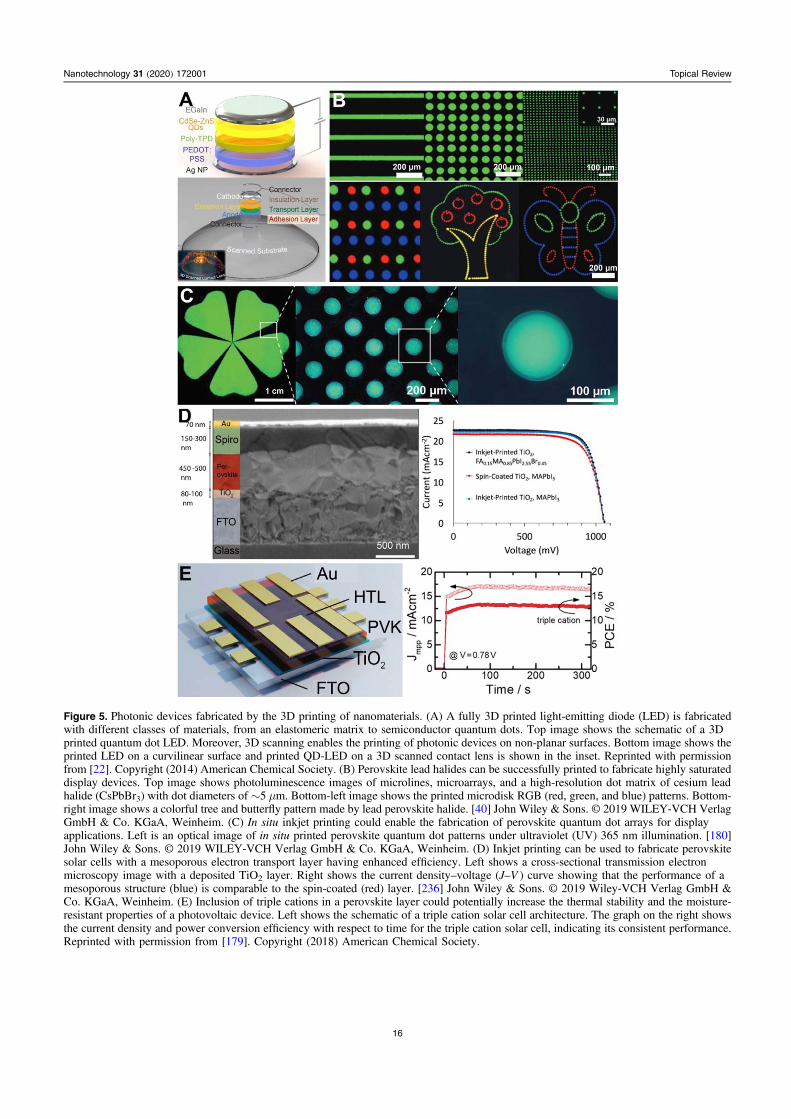
Figure 5. Photonic devices fabricated by the 3D printing of nanomaterials. (A) A fully 3D printed light-emitting diode (LED) is fabricatedwith different classes of materials, from an elastomeric matrix to semiconductor quantum dots. Top image shows the schematic of a 3Dprinted quantum dot LED. Moreover, 3D scanning enables the printing of photonic devices on non-planar surfaces. Bottom image shows theprinted LED on a curvilinear surface and printed QD-LED on a 3D scanned contact lens is shown in the inset. Reprinted with permissionfrom [22]. Copyright (2014) American Chemical Society. (B) Perovskite lead halides can be successfully printed to fabricate highly saturateddisplay devices. Top image shows photoluminescence images of microlines, microarrays, and a high-resolution dot matrix of cesium leadhalide (CsPbBr3) with dot diameters of ∼5 μm. Bottom-left image shows the printed microdisk RGB (red, green, and blue) patterns. Bottom-right image shows a colorful tree and butterfly pattern made by lead perovskite halide. [40] John Wiley & Sons. © 2019 WILEY‐VCH VerlagGmbH & Co. KGaA, Weinheim. (C) In situ inkjet printing could enable the fabrication of perovskite quantum dot arrays for displayapplications. Left is an optical image of in situ printed perovskite quantum dot patterns under ultraviolet (UV) 365 nm illumination. [180]John Wiley & Sons. © 2019 WILEY‐VCH Verlag GmbH & Co. KGaA, Weinheim. (D) Inkjet printing can be used to fabricate perovskitesolar cells with a mesoporous electron transport layer having enhanced efficiency. Left shows a cross-sectional transmission electronmicroscopy image with a deposited TiO2 layer. Right shows the current density–voltage (J–V ) curve showing that the performance of amesoporous structure (blue) is comparable to the spin-coated (red) layer. [236] John Wiley & Sons. © 2019 Wiley‐VCH Verlag GmbH &Co. KGaA, Weinheim. (E) Inclusion of triple cations in a perovskite layer could potentially increase the thermal stability and the moisture-resistant properties of a photovoltaic device. Left shows the schematic of a triple cation solar cell architecture. The graph on the right showsthe current density and power conversion efficiency with respect to time for the triple cation solar cell, indicating its consistent performance.Reprinted with permission from [179]. Copyright (2018) American Chemical Society.
16
Nanotechnology 31 (2020) 172001 Topical Review

area and reported to have greater than 18% conversionefficiency. Figure 5(D), left shows the cross-sectional SEMimage of the perovskite solar cell, where the mesoporoustitanium dioxide (TiO2) and perovskite absorber were inkjet-printed and HTL was spin coated. They optimized the dropspacing between the inkjet-printed droplets, temperature, andpercent of titanium di-isopropoxide bis(acetylacetonate)(TAA) in TiO2 ink to enhance the short circuit current andopen circuit voltage between the electrodes. Figure 5(D), rightshows the comparison of photovoltaic performance of inkjet-printed TiO2 in mixed (FA0.15MA0.85)Pb(I2.55Br0.45), spincoated TiO2, and inkjet-printed TiO2 in pure methylammo-nium lead iodide (MAPbI3). Mesoporous films for pureMAPbI3 absorber layers enhance the device performance dueto improved short circuit current.
In addition, 3D printing can offer control over thecrystallization behavior of perovskite layers, which is criticalfor the performance and lifetime of a solar cell device—such asin the creation of air-stable solar cell devices [245, 246].Typically, perovskite solar cells are sensitive to moisture andillumination to UV light, which are found to decrease theirlifespan. The use of triple cation perovskite with a small amountof cesium (15%) added to the perovskite is found to improvethe thermal stability and moisture resistivity. For example,Mathies et al [179] inkjet printed a mixed cation perovskitelayer on top of an electron transport layer, namely TiO2. Theschematic diagram shown in figure 5(E), left shows theschematic of a stack of layers, including glass, fluorine-dopedtin oxide (FTO), TiO2, triple cation perovskite (PVK)/spiro-MeOTAD as the hole transport layer, and Au electrode. Theright image shows that the power conversion efficiency of thetriple cation perovskite solar cells remains unaltered at 23 °Cfor 300 s. For further details and discussion on the enhancementof the stability of solar cells, the reader is referred to severalexcellent reviews [245–248] which provide in-depth discussion.
In summary, the 3D printing of nanomaterials is apromising approach to complement microfabrication processesand enable the creation of unique electronic devices, such ashigh performing energy storage devices; photonic devices; andflexible, wearable, and textile electronics. For example, 3Dprinting allows for the customization of device geometries, theintegration of hierarchical geometries, and direct printing onflexible substrates and materials which are otherwise incompa-tible with a conventional fabrication approach.
4.2. Biomedical devices
A biomedical device is defined as any instrument, apparatus,machine, appliance, or implant intended for medical purposes[249]. They are used for diagnosis, monitoring, or treatmentof diseases as well as the support of vital functions. Someexamples of biomedical devices include cardiac pacemakers,vascular stents, and surgical sutures. The biomedical deviceindustry is massive, expected to be valued at 409.5 billiondollars by 2023 [250]. 3D printing has enabled the creation ofbiomedical devices that are capable of addressing a widerange of unmet clinical needs due to its ability to fabricate
personalized constructs and prototypes [34]. For example, 3Dprinting has enabled the creation of biosensors [251],implants [252], prosthetics [253], and tissue engineeringconstructs [254]. Recent advances in novel 3D printingtechnologies have vastly expanded the capability to fabricatenovel biomedical devices. In particular, the incorporation ofnanomaterials to the 3D printing process is an attractiveapproach to modulate mechanical, geometric, biological, orresponsive properties in biomedical devices.
4.2.1. Customization of mechanical properties. Mechanicalproperties such as elasticity, stiffness, and tensile strength areimportant considerations for biomedical devices. For example,achieving mechanical properties that match that of nativetissues has been a longstanding goal in tissue engineering[255]. In orthopedics, significant interest has been devoted todeveloping specialized implants with engineered Young’smodulus that match the mechanical properties of bones[256]. Stress shielding occurs when the mechanical strengthof an implant surpasses that of bone, which leads to boneresorption and an increased risk of future fracture [257]. Inorder to remedy this issue, implants with mechanical propertiesthat are similar to bone are desirable. While these examples arenot the only applications of mechanical properties inbiomedical devices, they highlight the need to engineer themechanical properties of medical devices.
Nanomaterials are capable of modulating the mechanicalproperties, such as tensile strength, of 3D printed biomedicaldevices [258–260]. For example, Sezer et al demonstratedthat the integration of multiwall carbon nanotubes(MWCNTs) into acrylonitrile butadiene styrene (ABS)polymers could produce prints with superior tensile strength[261]. Varying concentrations of MWCNTs were tested fortensile strength (figure 6(A)). Their findings demonstratedthat the dispersion of MWCNTs resulted in superiormechanical strength up to 7 wt%. This improved tensilestrength expands the applications of this material to moreloadbearing uses. Other studies paired MWCNTs withpolybutylene terephthalate [148] and thermoplastic polyur-ethane [262] and reported similar improvements in mechan-ical properties. In addition, nanofillers such as calciumcarbonate and montmorillonite have been shown to improvethe mechanical strength of 3D printed structures as well [149].The addition of nanomontmorillonite to ABS increasedtensile strength from 29.5 to 37.1 MPa while the flexuralstrength increased from 54.8 to 64.2 MPa. These results wereconsistent with those obtained from injection-molded com-posites, suggesting that this reinforcement method iscomparable to similar methods used in traditionalmanufacturing.
Nanomaterials can also be used to enhance the mechan-ical strength of 3D printed hydrogels. Zhai et al usednanoclay-embedded poly (N-acryloyl glycinamide) to 3Dprint a bone scaffold [263] where the incorporation ofnanoclays increased the physical cross-linking of the polymerchains. This crosslinking improved the tensile strength,
17
Nanotechnology 31 (2020) 172001 Topical Review

Young’s modulus, and maximum strain of the 3D printedhydrogel construct (figure 6(B)). Hydrogels have long beeninvestigated for use in tissue scaffolds due to theirbiocompatibility; however, many hydrogels were unable tosupport significant weight. The incorporation of nanomater-ials into 3D printed hydrogels is an important advancement inbiomedical implants as it expands the applications of thesescaffolds.
Improved flexibility of printed devices is anotheradvantage that nanomaterial 3D printing can provide.Flexibility is an important quality for some devices in orderto function within the dynamic body without failing. Guineyet al printed a poly(lactic-co-glycolic acid) sheet withhexagonal boron nitride nanoparticles [41]. This sheet wasflexible and could be bent while still maintaining mechanicalstability (figure 6(C)). When testing different concentrationsof hBN, 3D printed structures showed an increase in strain tofailure percentage until 60% hBN. The authors suggest thatthe composite’s modular mechanical properties can haveapplications in many bioelectric technologies. When applyingthese findings to the broader 3D printing field, nanomaterialscan provide an important tool in developing 3D printedconstructs with desirable flexible properties.
In tissue engineering, the 3D printing of nanomaterialscan help replicate the mechanical properties of native tissues.Xu et al demonstrated how 3D printed nanocellulose could beused to create compressible cell scaffolds for wound healing[265]. Cellulose nanofibrils were integrated with gelatin tocreate noncytotoxic scaffolds that promote cell growth.Achieving this mechanical property is important in woundhealing because cell growth only occurs under specificconditions. Additionally, this study demonstrated that mod-ifying the ratio of cellulose nanofibrils and gelatin methacry-late allowed for a tunable Young’s modulus, suggesting thatmedical devices with engineered compressive properties canbe created for specific applications.
The integration of magnetic particles in a 3D printingprocess also provides an additional degree of control over themechanical properties in the pursuit of biomimetic mechan-ical properties [266]. Utilizing magnetic fields that orientanisotropic, magnetic nanoparticles in uniform directions,Martin et al fabricated architecture with supporting fibers thatdisplayed different responses to stress depending on theorientation of the nanoparticles [266]. High strength aluminananoparticles were coated with magnetic iron oxide particles.These nanomaterials were added to the printing reservoir of a
Figure 6. Nanomaterials can provide function mechanical properties to 3D printed constructs. (A) Acrylonitrile butadiene styrene (ABS)polymer embedded with MWCNT’s exhibit superior tensile strength up to 7 wt%. Reprinted from [261], Copyright (2019), with permissionfrom Elsevier. (B) 3D printed hydrogel scaffold exhibiting enhanced mechanical strength due to nanomaterials can be integrated into load-bearing applications such as bone. The N-acryloyl glycinamide hydrogel and nanoclay composite displayed properties that improve load-bearing applications. Reprinted with permission from [263]. Copyright (2017) American Chemical Society. (C) A poly(lactic-co-glycolicacid) (PLGA) sheet with hexagonal boron nitride maintains mechanical stability when bent. Reprinted with permission from [41]. Copyright(2018) American Chemical Society. (D) Electrically assisted 3D printed multi-walled carbon nanotubes (MWCNTs) are oriented in differentdirections in each layer, resulting in customizable, biomimetic mechanical properties. [264] John Wiley & Sons. © 2017 WILEY‐VCHVerlag GmbH & Co. KGaA, Weinheim.
18
Nanotechnology 31 (2020) 172001 Topical Review

DLP printer. Prior to polymerization, the field strengths ofthree orthogonal electromagnets were adjusted to create a 3Dmagnetic field. The magnetically active nanoparticles thenalign their long axis with the magnetic field vector. Thismethod facilitated the production of a heterogeneous structurewith anisotropic nanoparticles that were aligned in varyingspatial orientations. The manipulation of the physicalstructure produced constructs with nanomaterial alignmentthat could mimic biological architectures such as corticalbone. Such findings suggest the incorporation of externalmagnetic fields with 3D printing technologies can fabricateconstructs with mechanical properties similar to biologicaltissues.
In a similar mechanism to magnetically-oriented printing,electrically and shear-assisted 3D printing of nanomaterialscan be used to achieve biomimetic properties. In one example,electrically-assisted, nano-composite polymers were used todevelop personalized intervertebral disks [267]. Adjustmentof polymer composition with the electrical field allowed foroptimization of compressive properties that closely align withthat of trabecular bone. Applications of this concept couldinform medical implants that have personalized mechanicalproperties. Yang et al altered the mechanical properties of anartificial meniscus by using CNTs and electrically-assisted 3Dprinting to create a radially-aligned fibrous architecture(figure 6(D)) [264]. Specifically, they printed sheets ofalternatingly aligned MWCNT-embedded polymer. Thealternating orientation resembled that of a meniscus andprevented cracks from easily passing from layer to layer,effectively improving the impact resistance. Using shear-induced alignment of anisotropic cellulose nanocrystals,Siqueira et al replicated the directional mechanical reinforce-ment observed in cell walls [268]. They found that theorientation of the cellulose nanocrystal alignment played arole in the mechanical properties of printed matrices,including increased elastic modulus and tensile strength inthe direction of shear alignment. This finding suggests thatshear-induced patterning can be used to develop productswith direction-specific mechanical properties.
4.2.2. Customization of geometric properties. Additivemanufacturing methods have the ability to fabricate uniquegeometries that are not possible with conventional subtractiveor formative manufacturing techniques [34]. The geometry ofa printed product can dictate many functional properties of adevice, so the ability to fabricate precise geometries is aninterest for medical devices. For example, Lee et aldemonstrated the versatility of 3D printing by using PEGsacrificial scaffold to develop complex geometries withoverhanging architecture and porous regions [269]. Inaddition, computer imaging such as CT scans can be usedin conjunction with 3D printing to produce personalized,anatomic models [270]. These models can informpersonalized medical devices that match the anatomy ofindividuals [271]. The incorporation of nanomaterials furtherextends the versatility of 3D printing in these aspects. Forexample, it can expand the range of practical materials,
generate high-resolution structures, and produce customizedmedical devices.
First, incorporation of nanomaterials can enable the 3Dprinting of complex structures with materials that otherwisecannot be practically 3D printed. Abouzeid et al usedcellulose nanofibrils in conjunction with alginate hydrogelsto create scaffolds with complex geometries [272]. As purealginate hydrogels often do not have the viscosity necessaryto sustain self-supporting complex structures, the nanoparti-cles play an important role in enabling this feat. Thiscomposite has been used to replicate the structures of ear andbone, as shown in figure 7(A). Similarly, Wilson et al usednano silicates in a printable bioink that enable the 3D printingof both an ear and a nose [273] (figure 7(B)). Indeed, theincorporation of nanomaterials enables the creation of a self-supporting structure with a wider range of materials, enablingthe fabrication of more complex architecture.
Second, the 3D printing of nanomaterials can also allowfor the construction of high-resolution freeform architectures.Saleh et al utilized aerosol jet printing to 3D print metalnanoparticles into a well-defined, micro lattice architecture.For example, lattice structures with octahedral and hexagonalunit cells were constructed with a total length of 100, 200, and300 μm. They also demonstrated the versatility of thisprinting technique by building spatial interconnects, columns,and a dome. The applications of this printing method andmaterials could be extended to many fields such as tissueengineering, microfluidics, and microelectronics, whichrequire precise architectures.
When combined with advanced medical imaging, 3Dprinting of nanomaterials can create personalized medicalimplants. These implants may include cardiac patches,prosthetics, or implants. The anatomy of each individualvaries, which limits the effectiveness of ‘one-size-fits-all’medical devices. Noor et al demonstrated the applicability of3D printing nanomaterials by developing a personalizedcardiac patch [42]. A cardiac patch is a tissue engineeringconstruct that replaces damaged tissue in patients [276]. Itmust be elastic in order to withstand the movement of theheart, and it must allow cell growth and vascularization.Using CT scans of the patient’s heart, Noor et al used majorblood vessels to orient the heart and 3D print a cardiac patchspecific to that patient [42]. This collagenous nanofiberscaffold was seeded with cells from the patient, creating aconstruct that addresses both geometric and biochemicalrequirements. Computer modeling complemented the printingprocessing by preparing appropriate spacing for vasculariza-tion. Noor et al also used the same bioprinting technique withcollagenous nanofibers to produce a miniaturized heart ofthick vascularized tissue (figure 7(C)). The proof of conceptwas printed in a supporting bath and exhibited cellularization.
3D printing of a nanomaterial-based medical device alsoenables the creation of personalized prosthetics. In a paper byTong et al, a customized arm prosthetic is designed for apatient with an upper limb deformation [274]. 3D scans of thepatient’s limb informed the modeling of the implant andpressure sensors. After a prosthetic was designed to conformto the patient’s unique anatomy, a customized sensor was
19
Nanotechnology 31 (2020) 172001 Topical Review

printed to improve patient control. Multi-walled carbonnanotube ink was designed to conform to the shape of thepatient’s limb, and this paste could detect patient movementand facilitate control of the implant. Figure 7(D) shows howthe customizability of 3D printing conformed to the uniqueanatomy of the patient. The personalized interface betweenarm and prosthetic showed a 408% improvement in contactarea compared to non-personalized designs, which resulted inimproved control by the patient.
Finally, the 3D printing of nanomaterials can fabricatecustomized support structures. Ma et al added nanohydrox-yapatite crystals to 3D printed titanium alloys to developpersonalized implants for orthopedic healing [275]. Tradi-tional titanium implants often vary from complex nativebones in terms of mechanical strength and geometric shape.3D printing of titanium alloy supplemented with nanohy-droxyapatite can address both issues. The product exhibitedYoung’s modulus like bone, and CT scans informed designsthat geometrically matched personalized injuries. Figure 7(E)demonstrates how 3D imaging can inform the design ofimplants for improved geometric fit. The application ofpersonalized devices could be expanded to general popula-tions to ensure that every patient is receiving optimalhealthcare.
4.2.3. Customization of biological properties. Earlygenerations of biomedical implants relied on bioinertmaterials to improve biocompatibility. Current biomedicaldevices can be designed to elicit specific biological responses
[277]. This has potential applications in the field ofregenerative medicine [12, 43]. Implantable scaffolds can bedesigned to provide the necessary environment for celldifferentiation and proliferation and to restore thefunctionality of the tissue [12]. Utilizing nanomaterials, 3Dprinted constructs can mimic biological tissues, improve cellviability, and illicit specific biological activities.
The integration of nanomaterials with 3D printing couldfabricate constructs that mimic specific biological structures.Apelgren et al used bacterial nanocellulose to 3D print areplacement for human cartilage [278]. They found thatstructures produced by this method resembled the mechanicaland biological conditions found in natural cartilage. Inanother example, Markstedt et al [279] prepared bioink withnanofibrillated cellulose (NFC) and alginate. By combiningthe shear-thinning capability of NFC and fast curing cross-linking property of alginate, they successfully 3D bioprinted asheep meniscus with soft tissue and cells. Figure 8(A)illustrates the cell viability of human chondrocytes. Thismethod could lend itself to other bioprinting techniques,expanding the viability of 3D printed tissues. Also,Narayanan et al combined geometric and biologic 3Dbioprinting to develop an artificial meniscus seeded withhuman adipose-derived stem cells [280]. A PLA nanofiber-alginate hydrogel was used as the scaffold material andprinted into the shape of a human meniscus. Figure 8(B)shows the final print as well as images of the scaffoldstructure and cell staining. These images, which were takenfour weeks after seeding, provide evidence that nanomaterial
Figure 7. 3D printed constructs with complex geometric properties fabricated using nanomaterials. (A) Cellulose nanofiber prints can produce avariety of complex geometric products. Structures include the bone, ear, cube, cylinder, and boat. Reprinted with permission from [272].Copyright (272) American Chemical Society. (B) Bioink containing nanosilicates and kappa-carrageenan can print self-supporting anatomicalstructures such as a nose or ear. Reprinted with permission from [273]. Copyright (3017) American Chemical Society. (C) Bioprinted thick-vascularized tissue in a support bath mimics the shape of a miniature heart. Leftmost image shows the printing in a support bath. Center imageshows the heart, and the right image is a confocal image which demonstrates cellularization. Reproduced from [42]. CC BY 4.0. (D) 3D printedprosthetic for a patient with an upper limb deformity using CNT ink as a pressure sensor. The patient had a unique hand deformity, but 3Dprinting the prosthetic allowed for customized sensors for improved control. Reproduced from [274]. CC BY 4.0. (E) Customized titaniumimplant coated with nanohydroxyapatite made to fit bone defects. CT scans were used to inform the geometric design of the implant, improvingthe fit within the body. Reprinted with permission from [275]. Copyright (2018) American Chemical Society.
20
Nanotechnology 31 (2020) 172001 Topical Review

Figure 8. 3D printing of nanomaterials influences the biological properties of the construct. (A) Bioprinting of human chondrocytes withnanocellulose (hNC). Viability of hNC before (left and middle right) and after (right and middle left) 3D bioprinting. Here, red indicated deadcells, and green indicates live cells. Images demonstrate the feasibility of bioprinting living cells. Reprinted with permission from [279].Copyright (2015) American Chemical Society. (B) 3D printing of meniscus using alginate nanofiber bioink supplemented with humanadipose-derived stem cells. From left to right, anatomically shaped meniscus, image highlighting the distribution of cells and nanofibers, thecell viability on the external region of the construct after four weeks in culture, and the cell viability on the internal region of the constructafter four weeks in culture. Reprinted with permission from [280]. Copyright (2016) American Chemical Society. (C) Illustration of a braidednanofibrous scaffold. Electrospun poly(lactic acid) (PLLA) was used to mimic biological tendons and could support the growth of humanmesenchymal stem cells. The mechanical strength of the scaffold was dependent on the combination of nanofibers and number of nanofibersin a bundle. Therefore, these structures can be designed to match specific mechanical properties within the body. Reproduced with permissionfrom [281]. © Copyright 2013, Mary Ann Liebert, Inc. (D) Bioactive gold nanoparticles enhance human adipose-derived stem cell growth in3D printed scaffolds 24 h after seeding. From left to right, cell growth on gelatin hydrogel, cell growth on gelatin hydrogel supplementedwith gold nanoparticles, and cell growth on gelatin hydrogel supplemented with peptide conjugated gold nanoparticles. Reproduced from[282] with permission of The Royal Society of Chemistry. (E) SEM imaging of piezoelectric nanocomposite (left). In the closeup image ofthe Osteo-Print (right), barium titanite nanoparticles (BTNPs) on the surface of the 3D structure is observed. These nanoparticles give thecomposite piezoelectric properties which can be exploited by ultrasonic waves to improve osteogenesis. Reprinted with permission from[283]. Copyright (2015) American Chemical Society. (F) SEM image of 3D printed calvarial bone construct. The construct included humanamniotic fluid-derived stem cells that were cultured for 10 d. After five months of implantation, the implant exhibited vascularized bonetissue. Reprinted by permission from Springer Nature Customer Service Centre GmbH: Springer Nature, Nature Biotechnology, [43],2016. (G) SEM image of the PEO-PCL scaffolds with selective cell attachment. The construct was printed using a solvent-basedelectrohydrodynamic 3D printing process which allowed for high-resolution printing of polymer. Left figure shows scaffold embedded withMWCNTs with reduced cell adhesion. Right figure shows improved cell adhesion without MWCNTs. Reproduced from [284]. © IOPPublishing Ltd. All rights reserved. (H) 3D printed silver nanowire composites limit E. coli bacterial growth after 2 h. Applications ontoimplantable medical devices could help reduce infection. Reprinted from [285], Copyright (2019), with permission from Elsevier.
21
Nanotechnology 31 (2020) 172001 Topical Review

3D printing has applications in facilitating cell growth onprinted scaffolds.
3D printed nanofibers can also enable the creation oftendon and ligament (T/L) tissue scaffolds. Indeed, the slownatural recovery of T/L injuries often results in scar-liketissue with poor performance. Current surgical treatment suchas tissue gaping [286] and synthetic or allografting [287]exhibit limited long-term biocompatibility, durability, andfunctionality [281]. Barber et al [281] fabricated braidednanofibrous scaffolds (BNFSs) for constructing T/L tissue byelectrospinning poly(L-lactic acid) (PLLA). The printednanofibers were braided into 3, 4, or 5 aligned bundles toconstruct T/L tissue engineering scaffolds (figure 8(C)). Theauthors highlight the applicability of BNFSs to replacespecific tendons and ligaments, as the range of Young’smoduli for the tissue engineering scaffolds (47.6–55.0 MPa)could match the requirements of various native tendons andligaments. Additionally, the cell alignment of humanmesenchymal stem cells that were seeded onto the scaffoldaligned parallel with the nanofibers similar to tendons andligaments, suggesting that this scaffold design could assist inprogrammed cell growth.
Nanomaterials can also improve cell viability of bioinksformulated for 3D printing. For tissue scaffolds to attainwidespread use, they must support the growth of embeddedcells. Heo et al developed a bioactive bone scaffoldconstructed of polylactic acid (PLA), gelatin hydrogel, andpeptide-conjugated gold nanoparticles (RGNPs) [282]. Invitro studies suggest that (RGNPs) enhanced cell adhesionand proliferation on the construct as the cell area of the gelembedded with RGNPs had almost double the cell area after24 h of seeding and exhibited significantly higher stem cellproliferation rates (figure 8(D)). Another group used bioactivenanoparticles embedded in a cell scaffold to improve cellviability [135]. Poly(lactide-co-glycolic) acid (PLGA) nano-spheres encapsulated with transforming growth factor β1(TGF-β1) functioned as bioactive nanomaterials, which wereembedded into a polyethylene glycol diacrylate (PEG-Da)scaffold. This scaffold was SLA printed and seeded withhuman mesenchymal stem cells (hMSC). When measuringthe growth of hMSC in vitro, Castro et al found that thesenanomaterials helped facilitate chondrogenic differentiation,as the TGF-β1 sample showed 25% increase in type IIcollagen—a marker of chondrogenic differentiation. Theauthors speculate that the flexible nature of their 3D printingprocess could readily fabricate a variety of tissue scaffolds,demonstrating its applicability in tissue engineering.
In another example, piezoelectric nanoparticles can beco-printed to augment cell growth in the scaffold. Marinoet al [283] printed a bio-inspired 3D scaffold via two-photonpolymerization using piezoelectric barium titanite nanoparti-cles (BTNPs) embedded in the Ormocorp resist structure(figure 8(E)). In this study, ultrasound waves served as apiezoelectric stimulator, and this stimulation combined withBTNP’s suggested increased rates of osteogenesis based onthe expression of a protein that is upregulated duringosteogenesis. The structure with BTNPs and ultrasoundstimulation exhibited protein deposits on approximately
0.7% of the surface area while the sample without the BTNPshad 0.3% of the surface area.
3D printing with nanoparticles could also provide afabrication approach to create microchannels to mimicvascular constructs. Indeed, vascularization remains a promi-nent challenge to achieve successful tissue regeneration in a3D construct. Kang et al [43] have developed a custombioprinting technique for fabricating human-scale tissueconstructs in which microchannels are co-printed in tissuescaffolds to ensure diffusion of nutrients for cell viability. Asan example, they successfully fabricated calvarial bone madeof polycaprolactone (PCL) doped with tricalcium phosphate(TCP) nanoparticles (figure 8(F)). This structure was designedto improve vascularization, which is achieved after 5 months.Similar methods can be incorporated into other tissuescaffolds in order to improve biocompatibility.
Other studies have used nanoparticles integrated with 3Dprinted tissue scaffolds to elicit specific biological responses. Inthese examples, specific bioactive nanoparticles were used togenerate bioactive scaffolds. Kolan et al demonstrated theefficacy of using 3D printed bioactive borate glass in cellscaffolds [288]. Bioactive glass facilitated binding betweenimplants and the body and is resorbed back into the body at afaster rate compared to other scaffolds. Implementing bioactiveglass into the cell scaffold increased the porosity of the printand accelerated weight loss in vitro, both of which are desirablequalities. This allowed for quicker healing and decreaseddependence on the implant. To promote stem cell proliferation,Jakus et al used an extrusion method to fabricate a graphenescaffold [153]. This method used 60 vol% of graphene inpolylactide-co-glycolide (PLGA) to support human mesench-ymal stem cells in vitro. When comparing biological markersof glial and neurogenic cells, Jakus et al found that after 14 d,the scaffold with graphene exhibited between 2 and 6 times theamount of these markers compared to a 20 vol% graphenescaffold, suggesting that the concentration of this nanomaterialcould regulate stem cell proliferation.
Integrating nanomaterials with electrospinning can yieldthe creation of multi-scale tissue scaffolds with selective cellattachments. He et al [284] fabricated a microscale poly (ε-caprolactone) (PCL) scaffold with multi-walled carbon nano-tubes (MWCNTs) reinforcement (figure 8(G)) in which theaddition of polyethylene oxide (PEO) to PCL was studied toachieve an optimal PEO-PCL composition. This printingprocess controlled the area of cell growth on scaffoldconstructs as they found that cells on the PEO-PCL-MWCNTsscaffold only attached cells along the printed microfibers, whilethe PEO-PCL scaffold did not show this selectivity. Theauthors hypothesized that the agglomeration of MWCNTs inthe microscale fibers might have prevented cell attachment.This selective cell activity can be utilized in future scaffoldsthat wish to constrain cell growth to certain areas.
Infection is a serious risk that implantable medicaldevices carry [289]; however, 3D printing of nanomaterialscan help restrict bacterial growth on printed surfaces.Bayraktar et al demonstrated how silver nanowire PLAnanocomposites effectively protected implants againstS. aureus and E. coli bacteria (figure 8(H)) [285]. Specifically,
22
Nanotechnology 31 (2020) 172001 Topical Review

silver nanowires with only 1 wt% were able to kill 100% of S.aureus up to four hours; however, increasing the silverconcentration to 2 or 4 wt% could extend this duration. Whenapplied to a 3D printing process, these methods are promisingto minimize opportunistic infections of medical implants,such as total joint replacement prosthesis, by coating thesurfaces of medical devices with bactericidal nanocomposites.
4.2.4. Customization of responsive properties. 4D printing, aprocess by which 3D printed structures can change shape afterfabrication, has been shown to have many potentialapplications in the biomedical field [290]. Materials anddevices fabricated by 4D printing demonstrate responsiveproperties to certain stimuli. The mechanism for inducing a4D effect in a 3D printed product relies upon the use of smartmaterials, which can change shape when introduced to anexternal stimulus [291]. Nanomaterials can be incorporated ina 3D printing method to develop 4D properties within printedconstructs. When an appropriate force or an external stimulus,such as optical illumination or electrical actuation, is imposedin a nanomaterial, a change in shape or a change of theconstruct can be induced.
Nanomaterials such as graphene, carbon nanotubes(CNTs) and silica can be incorporated in 3D printing toinduce 4D effects [290]. Among other materials, polymers arean attractive smart material for 3D printed biomedical devicesbecause of their biocompatibility and printability [292].During printing, crosslinking develops within the polymer,which forms a permanent structure. After printing, thematerial can be molded to a different temporary shape. Thepolymer will maintain this temporary shape until it is heated
above its glass transition temperature, at which point it willreturn to its original shape. This property can be used todesign structures that move in response to certain stimula-tions. For a schematic explanation, see figure 9(A). Nano-materials can be incorporated into 3D printing to develop 4Dproperties within printed constructs. This section will reviewhow these constructs could inspire unique biomedical deviceswhen stimulated by heat, light, water, or magnetism.
First, temperature-responsive nanomaterials can be usedto induce 4D properties in 3D printed products. Mechanicalproperties are highly dependent on the material temperature,and this quality can be exploited to produce products whichhave dynamic mechanical properties. When Guo et alincorporated silica nanoparticles with poly (N-isopropylacrylamide) PNIPAM, the composite experienced a solid torubber transition at higher temperatures [294]. Both storageand loss modulus increased dramatically with the addition of10 wt% silica nanoparticles, which allows for the printingof complex geometries. As seen in figure 9(B), the addition ofsilica nanoparticles alters PNIPAM’s mechanical properties.Temperature-dependent 4D properties can also be used tomake water harvesting devices. Thakur et al used thermo-responsive nanomaterials to create water harvesting nanofi-bers [295]. Two different fibers were made with celluloseacetate (CA) and PNIPAM: one fiber was printed usingcoaxial electrospinning, which uses two materials to create acore and shell structure, and the other fiber was blended andelectrospun. The water harvesting effect is dependent uponthe ability of PNIPAM to make a conformational change thatexposes more hydrophilic functional groups at lowertemperatures. As such, both core–shell and blended
Figure 9. 4D properties can be achieved by 3D printing of nanomaterials (A) Schematic of the general mechanism for polymer shapememory. (B) A lattice structure with silica nanoparticles that improves the mechanical properties of the poly(N-isopropyl acrylamide)(PNIPAM), which is thermoresponsive and can produce a 4D effect. (C) Micro-sized structures that possess actuation properties due to thephoto responsive properties of gold nanorods incorporated in the structures. (A) Reprinted by permission from Springer Nature CustomerService Centre GmbH: Springer Nature, Nano Research, [293], 2019. (B) [294] John Wiley & Sons. © 2019 WILEY‐VCH Verlag GmbH &Co. KGaA, Weinheim. (C) Reprinted with permission from [137]. Copyright (2019) American Chemical Society.
23
Nanotechnology 31 (2020) 172001 Topical Review
nanofibers were shown to have 190% and 30% weight gainrespectively. When the temperature was increased from 25 °Cto 40 °C, the core–shell fibers lost moisture and resulted in a57% weight loss. This tunability demonstrates how heat couldbe used in 3D printing of nanomaterials to induce changesafter printing.
Second, light-responsive drug delivery devices can befabricated with 3D printing of nanomaterials. Light respon-sive nanomaterials can endow the ability to induce shapechange by photothermally heating materials [296]. Light is anattractive stimulation method because it enables hightunability and precision via the regulation of intensity andwavelength [297–299]. Tiwari et al used electrospinning tocreate drug-loaded polycaprolactone (PCL) nanofibers [298].The PCL-drug composite nanofibers allowed for a greatersurface area to be covered with the photothermally activepolypyrrole (PPy) because of favorable electrostatic interac-tions. They reported up to 60% drug release after four periodsof near-infrared (NIR) light exposure, which demonstrateshow light can be used to stimulate 4D printed constructs. Thisprecise drug release could also improve antibiotic treatments[300]. Altinbasak et al used an electrospinning technique tofabricate mats from poly(acrylic acid) nanofibers and reducedgraphene oxide nanoparticles [157]. Photostimulation inducedswelling of the nanofibers which released the drug. In vivoskin infection experiments in mice confirmed that the matsreleased enough antibiotic to induce wound healing andprevent bacterial growth of Staphylococcus aureus. Thisstudy suggests that future drug delivery systems couldlocalize release to predetermined locations. Choi et al usedgold nanorods (AuNRs) and poly(d,l-lactic-co-glycolic acid)(PLGA) to fabricate electrospun, drug-releasable nanofibers[158]. AuNRs can convert photonic energy into thermalenergy, thus heating PLGA crosslinks with photonic stimula-tion. The heated crosslinks allowed for a 20% release ofdoxepin hydrochloride after 12 h. The nature of these AuNRsalso allowed for the modulation of fiber temperature based onthe power density of the light. Such customizability is veryattractive for drug delivery vehicles, where it can be difficultto release specific amounts of drug into a system.
Light-sensitive AuNRs also have also shown to haveapplications in functional devices. Using two-photon poly-merization, Chen et al fabricated ornate, micro-sizedstructures with AuNRs and a liquid crystalline elastomermatrix that rapidly changed shape upon photo stimulation[137]. The mechanism of actuation, however, is differentfrom the previously described mechanism because it utilizesliquid crystals (LC). Upon printing, LCs are aligned. DuringNIR stimulation, the LCs lose their alignment, allowing formovement of the elastomer. As seen in figure 9(C), the directlaser printing technique allows for the fabrication of micro-sized structures that possess actuation properties. Tissueengineering is another field of interest for 4D printing light-responsive nanomaterials. Cui et al created a polymer/graphene nanocomposite using FDM and extrusion techni-ques [293]. Graphene is an attractive nanomaterial for neuralcell proliferation as it is conductive and optoelectronic. Undera NIR stimulation, they reported a photocurrent of 0.3 μA
within the scaffold. This has potential applications inphysiological systems that utilize electric currents such asneural cells and cardiomyocytes.
Third, water-induced swelling can produce printedobjects with responsive properties. Gladman et al utilized ahydrogel composite to develop 4D architectures that couldfold and twist when placed in water [301]. The hydrogel inkwas composed of N,N-dimethylacrylamide, photoinitiator,nanoclay, glucose oxidase, glucose, and nanofibrillatedcellulose. When printed with shear-induced alignment, theseinks exhibited anisotropic swelling behavior. Applying theseproperties to a bilayer structure with variable print orienta-tions allowed for the fabrication of structures that would foldinto specific flower morphologies when wet. This studydemonstrates how the design of printing materials andmethods can be used to design responsive architectures.
Fourth, magnetic nanomaterials can provide 4D proper-ties for 3D printed drug delivery devices. Magnetic-responsive materials function similarly to light-responsivematerials as they both induce temperature change uponstimulation. Niiyama et al used this strategy to achieve highlylocalized chemotherapeutic drug release [302]. Magneticnanoparticles were combined with poly(NIPAAm-co-HMAAm) and printed. The localized 18% drug release wasachieved by changing the frequency of an alternatingmagnetic field about the device, which led to a movementamong the magnetic nanoparticles, increasing the temperatureof the nanofibers. They reported several advantages to thischemotherapeutic technique, including controllable heating atthe tumor site and localized drug delivery.
4D properties that are stimulated by magnetic fields alsohave applications in soft robotics. Zhu et al used a non-uniform magnetic field to impart 4D characteristics. Theyfabricated a poly(dimethyl siloxane) nanocomposite with ironnanoparticles and printed it using DIW [303]. Uponapplication of a magnetic field, they found that a temporaryshape was achieved in 0.7 s. This fast response time wasattributed to a low magnetic coercive force and high magneticpermittivity. These findings could impact the field ofbiomedical devices where faster actuation times are desired.Wei et al utilized a DIW printing method and printed amultilayered rectangular scaffold with composite poly(lacticacid)-based inks containing BP/PLA/DCM c-PLA and FeO3.They reported that the addition of FeO3 nanoparticles tocPLA ink increased its shape recovery ratio, magneticallystimulated functionality, and localized temperature controlcompared to standard PLA ink [304]. The improved shaperecovery ratio is due to the addition of cross-linking structuresin the nanocomposite. They proposed that their findings couldbe applied to an intravascular stent, which would shrink whenheated. After this stent is implanted, it would cool, expandingthe stent into position.
4.3. Bioelectronic devices
Electricity is an essential part of bodily function, ranging fromthe electrical signals sent from the brain via nerves to everypart of an organism, to the electrical signals that regulate the
24
Nanotechnology 31 (2020) 172001 Topical Review

activity of each cell or group of cells [305, 306]. With somuch of the body utilizing electrical signals to communicateand function, the ability to interface with biological electricityhas significant potential in the regulation and observation ofphysiological functions, as well as an unraveling the complexmechanisms of the biological system [307, 308]. Bioelec-tronics is a field generally defined as the merging of elec-tronics with biology, where electronic signals are exchangedbetween electronic devices and biology [309, 310]. The fieldwas pioneered in the 1970s by Luigi Galvani when he firstactuated a frog leg with an applied voltage [310] and hassince introduced devices such as cardiac pacemakers and deepbrain stimulators [311].
One of the key challenges in most bioelectronics ismaintaining long-term biocompatibility: protecting cell via-bility and the health of the organism, as well as preserving theperformances of the electronics in a complex and dynamicbiological microenvironment [312, 313]. This is especiallychallenging with conventional electronics where mechanical,material, and geometrical dichotomies prevent a seamlessmerging of the electronic devices with biological constructs.For example, biological organs generally have Young’smoduli 3–6 orders of magnitude smaller than that of micro-fabricated electronics [7, 312]. Furthermore, seamless inter-facing of bioelectronics with complex, non-planar biologicalgeometry [7] requires devices of similar or smaller scale thanbiological cells and tissues [309].
Nanomaterials can be integrated with a 3D printing pro-cess to enable the creation of devices with highly tunablefunctional properties [309, 314, 315] which overcome thedichotomy described above. For example, the multi-scaleadditive manufacturing approach enables a facile route to printelectronic elements that can be integrated with flexible andbiocompatible materials in complex geometries [7]. Thissection highlights the unique capability of this approach inintegrating biological systems with electronics. We will firstdiscuss the 3D printing of microelectrodes to interface elec-tronics with biological electrical signals. Next, we will describethe 3D printing of nanomaterial-based bioelectronic scaffoldsthat can potentially improve tissue and organ regeneration.Finally, we will highlight how this multi-scale approach cancreate unique nanomaterial-based biosensors and lab-on-a-chipdevices which would otherwise be challenging to fabricate.
4.3.1. Microelectrodes. Microelectrodes can interface withthe body’s neural pathways to either acquire electrical signalsor to provide electrical stimulation [310]. To maximizebiocompatibility in a complex biological microenvironment,microelectrodes need to be mechanically compliant andchemically inert [316, 317] which is challenging to beachieved with a microfabrication approach. This reviewfocuses primarily on the 3D printing of nanomaterial-basedmicroelectrode arrays (MEA), which can be fabricated withreduced production times, increased customization, improvedbiocompatibility, and at lower cost than traditional devices.
3D printing can significantly reduce the production timeof MEAs and enable significant customization. In contrast to
a single microelectrode, MEAs are often preferred due to theirimproved mass transport, response times, sensitivities, andlower limit of detection (LOD—the smallest amount of asubstance that can be detected in a solution) [318]. Yang et alfabricated aerosol jet printed MEAs using silver nanoparticleink and polymer traces [318]. They accurately controlled thespacing between conductive traces at 30, 100, and 180 μm,demonstrating the ease of customization with 3D printing instark contrast to a micromachining approach. Kundu et aldeveloped a process where complete 8×8 MEAs could beassembled in under 4 d [319] which otherwise would take upto four months with a conventional fabrication approach. Thisis achieved with an SLA printed clear base which issubsequently subjected to ink casting of a silver nanoparticleink, pulsed electroplating of either a gold or platinumsolution, and laser micromachining to produce the finishedpart. Although this approach is not entirely 3D printed andyields a lower resolution than traditional lithographicmethods, the incorporation of a 3D printing process enablesa rapid fabrication and prototyping approach (as shown infigure 10(A)), allowing a faster possible implementation intocustomized medical devices and constructs. The authors alsodemonstrated that the nanoporous platinum and nano-goldlayers can achieve a measured impedance and double-layercapacitance similar to commercially available MEAs (1 kHzimpedance of 36.8/16 kΩ and double layer capacitance of400 nF cm−2/520 nF cm−2 for nanoporous platinum/nano-gold, respectively).
A 3D printing approach, such as inkjet printing ofnanomaterial-based inks, can enable the creation of biocom-patible and flexible MEAs. Khan et al designed fullybiocompatible MEAs with inkjet-printed gold nanoparticleconductive traces, shown in figure 10(B) [110]. Gold isdesirable for biological applications due to its superiorstability when in contact with biological fluids and tissues.The use of gold nanoparticles also allowed them to selectivelysinter the traces on plastic substrates below the melting pointsof the plastics themselves. Low-temperature sintering wasperformed at approximately 200 °C and sintering time wascarefully tuned to ensure all traces were properly fused, astraces of different widths sinter at noticeably different speedsat low temperatures. After the inkjet traces were sintered, theMEAs were coated with a thin layer of fluoropolymer andthen plasma-etched to expose the electrode contacts. Thefluoropolymer provided additional protection for the viasfrom biological fluids [321].
Indeed, integrating a complete multi-material additivemanufacturing approach with nanomaterials can lead toreduced fabrication times, cost, and improved MEA biocom-patibility without compromising electrical performance.Although exhibiting unique performance, the 3D printedMEAs described earlier require conventional fabricationtechniques for a subset of the processes (e.g. post-processing)and are not entirely 3D printed. Recently, Schnitker et alleveraged a complete 3D printing approach to create highlycustomized MEAs in less than 60 min per chip and costingonly a few cents per chip [320]. Silver nanoparticles andnanoporous carbon conductive traces were printed on a
25
Nanotechnology 31 (2020) 172001 Topical Review

polyethylene naphthalate base; these were coated with adielectric polyimide in the final step to provide a protectivelayer, as shown in figure 10(C). The silver ink provided auseful conductive layer, but to avoid biological harm, it wasnot printed near the sensing area. Nanoporous carbon inkprovided superior biological compatibility as an interfacingmaterial, and can maintain electrical performance due to itschemical stability, low impedance, and large electrochemicalwater window (voltage range in which a chemical neitheroxidizes nor reduces) [44, 322]. Impressively, the authorsdemonstrated the versatility of their approach by 3D printingMEAs on a variety of materials including PDMS, agarose,
and complex gelatin structures (gummy bears) as shown infigure 10(D) [44].
4.3.2. Bioelectronic scaffolds. The integration of electricalcomponents with biological regenerative scaffolds could havea significant impact on the creation of biomedical devices. Forexample, studies have suggested the use of electrostimulationas a potential approach to promote the regeneration ofbiological tissues [323–325]. The incorporation of electronicsinto biological scaffolds could potentially enhance, modulateor even enable regenerative processes. Indeed, the merging of
Figure 10. 3D printed, nanomaterial-based microelectrode arrays (MEAs) can be fabricated with greater customization and improvedbiocompatibility than devices constructed using a conventional fabrication approach. (A) Rapidly prototyped 3×3, 6×6, and 8×8 MEAs, respectively. The arrays consist of an SLA printed base and silver nanoparticle traces. Reproduced from [319]. CC BY 2.0.(B) Flexible inkjet-printed MEAs. Gold nanoparticle traces are printed on a polyethylene naphthalate (PEN) substrate and encapsulated in aprotective fluoropolymer. Left shows the first step in the fabrication process, right and center show the completed MEAs. [110] John Wiley &Sons. © 2015 WILEY‐VCH Verlag GmbH & Co. KGaA, Weinheim. (C) Flexible and fully inkjet-printed MEAs consist of silvernanoparticle traces, exposed nanoporous carbon electrodes, and a polyimide protective layer. [320] John Wiley & Sons. © 2018 WILEY‐VCH Verlag GmbH & Co. KGaA, Weinheim. (D) Fully inkjet-printed MEAs on complex substrates such as gummy bears and gelatin.Center image shows an MEA printed on hydrogel and attached to a circuit board for action potential measurements of cell culture.Reproduced from [44]. CC BY 4.0.
26
Nanotechnology 31 (2020) 172001 Topical Review

electrical components with biological constructs is ofsignificant interest but has yet to be achieved due to theaforementioned challenges in merging conventionalelectronics with biological constructs. 3D printing ofnanomaterial-based devices is a promising approach thatcan potentially enable a better incorporation of electronicsinto a complex regenerative system.
One approach to achieve such integration is through thecreation of biocompatible scaffolds with imparted electricalconductivity. For example, Jakus et al developed a graphene-based polylactide-co-glycolide (PLG) scaffold [153] usingDIW 3D printing. The scaffold demonstrated electricalconductivities above 800 S m−1 and in vivo biocompatibilitywith a mouse subcutaneous implant model for 30 d. As aproof of concept, a nerve conduit was 3D printed andcharacterized, as shown in figure 11(A). It was found that theshear alignment of the graphene flakes during printingimproves the electrical conductivity and tensile strength(210 MPa at 20 vol% graphene) of the structure.
In addition to electrically conductive biomanufacturedscaffolds, a multiscale 3D printing approach also enables the
creation of electrically conductive devices into bioprintedconstructs, which can improve cell adhesion and proliferationover passive scaffolds. For example, using magnetic field-assisted electrospinning, Chen et al studied the effect ofaligned nanofibers by seeding mouse skeletal muscle tissue(myoblasts) on poly(e-caprolactone) (PCL) and PCL withpolyaniline (PCL/PANi) electrospun nanofibers [326]. Intri-guingly, they have shown that aligned, electrically conductivePCL/PANi nanofibers further increased myoblast numberand maturation index over aligned, nonconductive PCLnanofibers by approximately 30% and 3% respectively, asshown in figure 11(B). Similarly, Bolin et al coatedelectrospun nanofibers with conductive poly(3,4-ethylene-dioxythiophene) (PEDOT) and observed excellent adhesionand proliferation of neuronal cells on the scaffold, as shownin figure 11(C) [327]. Electrical stimulation further inducedCa2+ signaling between the cells.
In another example, Wang et al show that electrospunPLA/PANI conductive nanofibrous sheets can promote cellviability of cardiomyocytes (cardiac tissue) [329]. Cardio-myocytes seeded on conductive nanofibers had a higher
Figure 11. 3D printed bioelectronic scaffolds can aid in the regeneration of biological tissues and cells. (A) A 3D printed graphene scaffoldpromotes regeneration of the ulnar nerve, indicated by arrows, in a human cadaver. Reprinted with permission from [153]. Copyright (2015)American Chemical Society. (B) Electrospun nanofibers provide electrical and topographical cues to assist in the alignment and maturation ofmouse skeletal myoblasts. Reprinted from [326], Copyright (2013), with permission from Elsevier. (C) A neurite, indicated by the arrow,growing on a conductive electrospun scaffold. Reprinted from [327], Copyright (2009), with permission from Elsevier. (D) Electrospun,semiconductive, photosensitive PCL/PDBTT nanofibrous scaffolds for skin regeneration result in greater cell density with light stimulationthan do normal PCL scaffolds. Reprinted from [328], Copyright (2017), with permission from Elsevier. (E) A 3D printed bionic ear. Left toright shows a schematic, prototyped ear, and then the prototyped bionic ear experimental setup which is used to characterize the audiosensing of the ear. Far right shows a photographed cross section of the ear (top), and a fluorescent close-up image (bottom) showing theviability of the living chondrocytes that are in contact with the conductive electrodes. Reprinted with permission from [45]. Copyright (2013)American Chemical Society.
27
Nanotechnology 31 (2020) 172001 Topical Review

maturation index and fusion index than ones seeded on non-conductive PCL nanofibers. The fibers also beat synchro-nously with the cardiomyocytes, the cells stimulating thescaffold, an effect that could enable other bioelectronicapplications [330–332]. Liu et al electrically stimulatedMC3T3-E1 cells (bone tissue cells) on aniline pentamer-graft-gelatin (AP-g-GA) and poly(L-lactide) (PLLA) electro-spun nanofibers [333]. Although significant differences in thecells seeded on various nanofiber mats were not observed, ahigher [Ca2+]I (measured value to quantify the totalpopulation of cells) was observed for cells exposed toelectrical stimulation than for those that were not, and goodbiocompatibility was observed for all.
Photosensitive elements can also be 3D printed to enablelight-induced electrical stimulation. For example, Jin et alfound that the cell proliferation of human dermal fibroblasts(skin cells) increases on PCL/PDBTT electrospun nanofibers[328]. The photosensitive poly (N,N-bis(2-octyldodecyl)-3,6-di(thiophen-2-yl)-2,5-dihydropyrrolo[3,4-c]pyrrole-1,4-dione-alt-thieno[3,2-b]thiophene) (PDBTT) was stimulated with ared LED for one hour every 24 h, resulting in higher cell–cellcommunication and proliferation over PCL nanofibers.Figure 11(D) shows a comparison between stimulated andnon-stimulated human dermal fibroblasts on PCL and PCL/PDBTT nanofibers.
An entirely 3D printed electronic and regenerativescaffold can also be achieved with a multiscale 3D printingprocess. As a proof of concept, Mannoor et al fabricated abionic ear with DIW 3D printing [45]. Living chondrocyteswere seeded in a hydrogel matrix, printed in the shape of anear and co-printed with silver nanoparticles as a coiledantenna inside the ear, as shown in figure 11(E). This suggeststhe possibility to integrate biological constructs with func-tional electronics using a multi-scale 3D printing approach,allowing the creation of regenerative constructs integratedwith functional electronics.
4.3.3. Biosensors. Biosensors are devices that sense thepresence of a specific substance and produce a recognizableelectrical signal in response [334]. Although not allbiosensors interface with the body’s electrical signals,bioelectronics and biosensors are often treated together dueto how closely intertwined the fields are [335–337]. Glucosebiosensors are bioelectronic, for example, because they utilizeelectrodes to detect the number of electron transfers in acatalyzed glucose reaction [309, 338, 339].
The integration of nanomaterials into 3D printedconstructs can leverage their size-dependent functionalproperties to create tunable chemosensors. 3D printednanomaterial-based sensors have been demonstrated to beable to detect chemicals such as glucose [340], biomarkers[341–343], herbicides [343], and bacteria [344, 345]. Forexample, Su et al fabricated a multi-well glucose sensor byFDM printing two composite filaments consisting ofacrylonitrile butadiene styrene (ABS) and magnetite nano-particles, as well as polyvinyl alcohol (PVA) ando-phenylenediamine (OPD) [340]. They achieved this by
leveraging the water solubility of PVA to graduallyincorporate chromogenic OPD into the mixture. Whenexposed to hydrogen peroxide, OPD will undergo oxidationon the surface of the magnetite—used here as a nanoparticlecatalyst. The production of hydrogen peroxide from theoxidation of glucose provided a means of colorimetricobservation without the addition of other reagents to thesample (figure 12(A)). The further optimization of themicrostructures of the two-part plates, the incubationpH (∼5 pH), and temperature (∼40 °C) enables the creationof a reliable (∼±4.4% error) glucose monitoring device.
3D printing can also leverage the biocompatibility andchemical sensitivity of metallic nanomaterials to form flexibleelectrode arrays with a variety of uses, from amplifyingelectrical signals [346] to the detection of cancer markers[341, 342] and antioxidants [343, 347]. Using the precisionand multi-material capability of inkjet printing, complexelectrode arrays can be quickly fabricated using minimalmaterials, and customized to tune the sensor’s response. Forexample, Adly et al fabricated microgap electrodes for redox-cycling biosensors with carbon and silver nanoparticlescoated with polyimide ink [346]. The spacing betweenelectrodes determines the redox-cycling amplification ofelectrochemical signals and, subsequently, device sensitivity(figure 12(B)). Electrode spacing down to 1 μm was achievedby carefully controlling droplet ejection frequency, transla-tional velocity, and substrate temperature. Utilizing thesensitivity of the redox current to surface blocking, Adlyet al successfully demonstrated the electrochemical biosen-sing of human immunodeficiency virus (HIV)-related DNAstrands with their device. The high sensitivity of the electrodearray was made possible by the single-droplet precision ofinkjet printing. Similarly, Pavinatto et al inkjet-printedantioxidant biosensors with precisely sintered, interdigitatedgold electrodes (figure 12(C)) [343]. The gold nanoparticletraces were printed on plastic substrates and sintered at 200°C for 6 h, the finalized flexible sensors showing a limit ofdetection (LOD) of 200 μM. Furthermore, Jović et al inkjet-printed silver nanoparticles and CNTs to form an electrodearray, which could detect thyroid-stimulating hormone (TSH)in an aqueous solution and atrazine (ATR) in urine with asensitivity as high as 0.5 μUml−1 (TSH) and 0.01 μg l−1
(ATR) [348].Functionalized gold nanoparticle electrodes can be used
to detect cancer biomarkers. For example, Otieno et al inkjet-printed electrode arrays to detect parathyroid hormone-relatedpeptides (PTHrP), which have been utilized as biomarkers fora variety of cancers [341]. Biocompatible gold nanoparticleswere used in the eight-electrode array, which was able todetect both PTHrP and its fragments with an LOD of 150 aM—approximately 1000 times lower than conventional meth-ods. This impressive array was printed using only $0.20 ofmaterials, and 56 arrays could be printed in a single run.Carvajal et al used a similarly inexpensive method to printeight-electrode arrays for sensing HER-2, a breast cancerbiomarker [342]. They printed silver nanoparticle traces, goldnanoparticle electrodes, and coated the sensor with abiocompatible polyimide substrate, completely inkjet printing
28
Nanotechnology 31 (2020) 172001 Topical Review

the electrodes with the successful method discussed in themicroelectrode section above. The sensor had an assay timeof only 15 min and a LOD of 12 pg ml−1. Both devicesbehave similarly—rather than directly detecting the biomar-kers, the gold electrodes detect ferrous molecules in solutionthrough redox reactions at the electrodes’ surface. Both theelectrodes and the ferrous molecules (Otieno used iron beads,Carvajal used heme) are functionalized with antibodies, sothat the biomarkers will bridge the two and cause a redoxcurrent to flow. These 3D printed biosensors offer manyadvantages over conventional biosensors: they are inexpen-sive, exhibit small LODs, and their sensitivity can be tuned.
In addition to the functional properties of nanomaterials,the rapid prototyping ability of 3D printing enables theoptimization of biosensor performance in a variety of assayenvironments. CAD can be used to maximize the efficiency ofthe nanomaterial biosensor through techniques such as sortingbacteria and filtering complex mixtures. For example, size-based separation can be used to maintain the biosensor’sperformance when using suboptimal mixtures. Lesch et alwere able to produce an antioxidant biosensor that couldoperate in unfiltered, complex mixtures such as orange juiceand red wine [347]. Matrix effects normally necessitate thetreating of such samples with dilution or filtering before
Figure 12. 3D printed nanoparticles enable the creation of biosensors with tunable properties, that are mechanically flexible, and that candetect in a variety of assay environments. (A) FDM printed multi-well, glucose determining plates allow for colorimetric differentiationbetween urine from a healthy person (center), and urine from a diabetic person (right). Iron magnetite nanoparticles act as reusable catalystsimbedded in the wells. Reprinted from [340], Copyright (2018), with permission from Elsevier. (B) High-resolution inkjet-printed lines forredox cycling, with spacing controlled down to 1 μm. [346] John Wiley & Sons. © 2017 WILEY‐VCH Verlag GmbH & Co. KGaA,Weinheim. (C) Flexible, inkjet-printed, interdigital electrodes for antioxidant sensing. Bottom shows a magnified view of the goldnanoparticle electrodes. Reprinted from [343], Copyright (2015), with permission from Elsevier. (D) Simultaneous inkjet printing and UVphotopolymerization of polyacrylamide ink on CNTs and polyimide for the creation of antioxidant-sensing electrodes. Silver nanoparticles,CNTs, an insulator, and then polyacrylamide are printed sequentially to form the biosensors (shown below). Reprinted with permission from[347]. Copyright (2015) American Chemical Society. (E) A 2PP printed microscopic cage for motile bacteria. Center inset shows the bacteriaconcentration mechanism, right shows the sensors at the center of the cage. Reproduced from [345]. CC BY 4.0.
29
Nanotechnology 31 (2020) 172001 Topical Review
sensing, however a thin layer (50 nm–1 μm) of polyacryla-mide hydrogel (PA) acted as a screen for the CNT electrodes.Nanopores (∼13 nm) within the film permitted the passing ofantioxidant molecules while blocking unwanted substancessuch as pulp and fibers. The hydrogel film was optimized bytuning the surface tension and viscosity of the hydrogel, alongwith in situ UV curing. The entire device was inkjet printedwith four ink compositions (Ag, CNT, insulator, and PA).The multi-material inkjet process and finalized electrodes areshown in figure 12(D).
Intriguingly, a similar size-based sorting concept can beapplied to bacteria assays by integrating 3D printed micro-fluidics and magnetic nanoparticles. This approach enablesthe ability to actively remove and sort E. coli bacteria from asolution [344]. Specifically, magnetic nanoparticle clusters(MNCs) made of 15 nm magnetite nanoparticles arefunctionalized with antibodies which will bind onto thebacteria to form MNC-E. coli complexes (MNC-EC). Themagnetic properties of the magnetite particles allow theMNC-ECs to be separated from the food analog using amagnetic field. The solution of MNCs and MNC-ECs are thenforced through a 3D printed, helical microfluidic channel toseparate the MNC-ECs. The helical channel produces Deanvortices in the moving fluid which causes the smaller MNCsto migrate toward the outer edge of the helix. This allows theseparation of a concentrated MNC solution and a concen-trated MNC-EC solution. Thus, the mechanical removal ofE. coli bacteria from food is possible, as well as collection ofsamples for analysis. The authors show that this approachenables detection limits as low as 10 cfu ml−1 in buffer and100 cfu ml−1 in milk for E. coli with ultraviolet–visiblespectroscopy. Furthermore, the optimization of devicemorphology can be used to passively sort bacteria. Forexample, Li et al utilized two-photon polymerization (2PP) tocreate a microscopic cage for motile bacteria (figure 12(E)) toimprove the sensitivity of a graphene-based biosensor [345].Inspired by venous valves, selective photopolymerization wasused to fabricate a customized, directional valve system. Themorphology of the valve system facilitates the motion ofbacteria in only one direction, causing the bacteria toconcentrate in the sensing area. As the sensor detection isdue to the charge carrier density change when bacteria bind tothe surface, increasing the concentration of the bacterialenhances the detection rate. Indeed, electrical measurementsdemonstrated signal enhancement up to 27 fold. Theseexamples of 2PP, SLA, and inkjet 3D printed biosensorsshow the variety of applications and the robustness of 3Dprinting technology. Inexpensive and mechanically flexiblesensors can be printed quickly and with excellent finalsensitivities, and the 3D printing process allows for rapidcustomization.
4.3.4. Lab on a chip. Lab on a chip is generally defined asresearch with the goal of miniaturizing biological or chemicalprocesses, such as microfluidic chips or miniaturized sensorsand arrays (biochips) [349]. The fabrication of labs on a chiptypically utilize time-consuming, multi-step lithographic
processes [350]. The ability to seamlessly 3D print lab-on-a-chip devices could revolutionize biomedical and chemicalresearch, allowing for rapid customization and improved cellmonitoring.
The 3D printing of nanomaterial-based lab-on-a-chipdevices allows for rapid customization and increasedbiocompatibility. For example, Moya et al utilized the rapidcustomization of inkjet printing to fabricate a dissolvedoxygen sensor for a liver-on-a-chip device [351]. The lowtemperatures of inkjet printing allowed them to print ondelicate substrates with gold and silver nanoparticle inks. Thesensors were thin, flexible, and biocompatible, integratingseamlessly with the liver cell culture and microfluidicsrequired for the device. Although the microfluidic channelswere not 3D printed, the 3D printing of this portion couldenable faster fabrication times and customization of thedevice as a whole [352–354]. An entirely DIW printed lab ona chip was achieved by Lind et al which demonstrates boththe customization and biocompatibility achievable with thistechnology [46]. They printed soft strain gauge sensors in amicro-architecture that allows the growth of cardiac tissues.The printed device successfully measured the spontaneousbeating of seeded cardiac tissue over the course of a month aswell as the increasing strain exerted by the tissue as it grewand strengthened. During fabrication, a sacrificial 0.5 μmthick dextran film layer was printed first that would allow thestrain-gauge cantilevers printed next to detach for uncon-strained movement. 6.5 μm thick conductive carbon blacknanoparticles mixed in thermoplastic polyurethane (TPU)were then printed as the strain gauge wires within twoinsulating layers of plain TPU. Polydimethylsiloxane (PDMS)was printed next as a thicker supporting layer, followed byelectrical leads and contact pads printed with silver-nanoparticle polyamide (Ag:PA) ink. An insulating layerand eight individual wells were assembled on the sensors forseparate tissue examination. The entire process was com-pleted in a single continuous procedure with a four-nozzleDIW printer, with only some curing at 100 °C and subsequentcell seeding following the printing. This study illuminates thepossibilities afforded by completely 3D printed lab-on-a-chipdevices.
3D printed nanoparticles also allow for improved cellmonitoring. Apart from the various sensors that have alreadybeen discussed, nanoparticles have also been used as markersin oxygen and pH sensors [355], DNA sensors [356], andimmunoassays [357, 358]. One such nanoparticle sensor wasdemonstrated by Trampe et al through the bioprinting ofliving cells with oxygen sensing nanoparticles [359], whichallowed for effective cell monitoring. Luminescent styrenemaleic anhydride copolymer (PSMA) nanoparticles contain-ing an O2 luminescent indicator were DIW printed with greenmicroalgae and mesenchymal stem cells in basic scaffolds;this allowed for online monitoring of the metabolic activity ofthe cells using a simple single-lens reflex camera. The 3Dprinting process allows for the customized integration ofbiosensors with lab-on-a-chip devices, allowing for therapidly customized integration of different cell cultures andindicators into a single printed device.
30
Nanotechnology 31 (2020) 172001 Topical Review

5. Conclusion
This review highlights the advances of 3D printed nanoma-terial-based electronic, biomedical, and bioelectronic devices.First, we discussed the creation of 3D printed electronicsallowing their integration with complex geometries and onnon-planar, flexible and stretchable substrates. Second, weexplored how a nanomaterial-based 3D printing approach canimpart mechanical, geometric, biological, and responsiveproperties to biomedical devices, which enable the creation oftissue scaffolds, personalized medical devices, and drugdelivery devices. Third, we highlighted the creation of 3Dprinted bioelectronic devices such as microelectrodes, elec-trically stimulated tissue-regenerating scaffolds, and bio-sensors with enhanced sensitivity to describe the potentialimpact of this approach in the creation of highly integratedmultifunctional constructs. In summary, the advances of amulti-scale, multi-material 3D printing approach can enablethe freeform fabrication of nanomaterial-based devices byendowing unique optical, chemical, mechanical, and electricalproperties to otherwise passive constructs.
Acknowledgments
The authors acknowledge funding support in part from theDepartment of Mechanical Engineering of the University ofUtah as well as the National Science Foundation underEmerging Frontiers in Research and Innovation (EFRI) Pro-gram (Grant No. EFRI 1830958).
ORCID iDs
Yong Lin Kong https://orcid.org/0000-0003-0270-2068
References
[1] Frazier W E 2014 Metal additive manufacturing: a reviewJ. Mater. Eng. Perform. 23 1917–28
[2] Rayna T and Striukova L 2016 From rapid prototyping tohome fabrication: how 3D printing is changing businessmodel innovation Technol. Forecast. Soc. Change 102214–24
[3] Ngo T D, Kashani A, Imbalzano G, Nguyen K T Q and Hui D2018 Additive manufacturing (3D printing): a review ofmaterials, methods, applications and challenges CompositesB 143 172–96
[4] Cumpston B H et al 1999 Two-photon polymerizationinitiators for three-dimensional optical data storage andmicrofabrication Nature 398 51–4
[5] Kelly B E, Bhattacharya I, Heidari H, Shusteff M,Spadaccini C M and Taylor H K 2019 Volumetric additivemanufacturing via tomographic reconstruction Science 3631075–9
[6] Truby R L and Lewis J A 2016 Printing soft matter in threedimensions Nature 540 371–8
[7] Kong Y L, Gupta M K, Johnson B N and McAlpine M C2016 3D printed bionic nanodevices Nano Today 11 330–50
[8] Mcalpine M C and Kong Y L 2018 3D printed activeelectronic materials and devices US20160218287A1
[9] McAlpine M C, McAlpine M C, Sebastian-Mannoor M,Kong Y L and Johnson B N 2016 Multi-functional hybriddevices/structures using 3D printing US9517128B2
[10] Joshi S C and Sheikh A A 2015 3D printing in aerospace andits long-term sustainability Virtual Phys. Prototyp. 10175–85
[11] Attaran M 2017 The rise of 3D printing: the advantages ofadditive manufacturing over traditional manufacturing Bus.Horiz. 60 677–88
[12] Ghosh U, Ning S, Wang Y and Kong Y L 2018 Addressingunmet clinical needs with 3D printing technologies Adv.Healthcare Mater. 7 1800417
[13] Guzzi E A and Tibbitt M W 2019 Additive manufacturing ofprecision biomaterials Adv. Mater. 1901994
[14] Martelli N, Serrano C, Van Den Brink H, Pineau J,Prognon P, Borget I and El Batti S 2016 Advantages anddisadvantages of 3-dimensional printing in surgery: asystematic review Surgery 159 1485–500
[15] Patra S and Young V 2016 A review of 3D printingtechniques and the future in biofabrication of bioprintedtissue Cell Biochem. Biophys. 74 93–8
[16] Schubert C, Van Langeveld M C and Donoso L A 2014Innovations in 3D printing: a 3D overview from optics toorgans Br. J. Ophthalmol. 98 159–61
[17] Ursan I, Chiu L and Pierce A 2013 Three-dimensional drugprinting: a structured review J. Am. Pharm. Assoc. 53136–44
[18] Kong Y L et al 2019 3D-Printed gastric resident electronicsAdv. Mater. Technol. 4 1800490
[19] Rengier F, Mehndiratta A, Von Tengg-Kobligk H,Zechmann C M, Unterhinninghofen R, Kauczor H U andGiesel F L 2010 3D printing based on imaging data: reviewof medical applications Int. J. Comput. Assist. Radiol. Surg.5 335–41
[20] Randazzo M, Pisapia J, Singh N and Thawani J 2016 3Dprinting in neurosurgery: a systematic review Surg. Neurol.Int. 7 801
[21] Heinrich M A et al 2019 3D bioprinting: from benches totranslational applications Small 15 1970126
[22] Kong Y L, Tamargo I A, Kim H, Johnson B N, Gupta M K,Koh T W, Chin H A, Steingart D A, Rand B P andMcAlpine M C 2014 3D printed quantum dot light-emittingdiodes Nano Lett. 14 7017–23
[23] Zhang D, Chi B, Li B, Gao Z, Du Y, Guo J and Wei J 2016Fabrication of highly conductive graphene flexible circuitsby 3D printing Synth. Met. 217 79–86
[24] Wei P, Yang X, Cao Z, Guo X L, Jiang H, Chen Y,Morikado M, Qiu X and Yu D 2019 Flexible and stretchableelectronic skin with high durability and shock resistance viaembedded 3D printing technology for human activitymonitoring and personal healthcare Adv. Mater. Technol. 241900315
[25] Kong Y L 2019 Transforming military medicine with 3Dprinted bioelectronics Homel. Def. Inf. Anal. Cent. 6 34–8
[26] Mohammed M G and Kramer R 2017 All-printed flexible andstretchable electronics Adv. Mater. 29 1604965
[27] Yu F et al 2019 Real-time manipulation of intestinalperistalsis by enteric-encapsulated magnetic nanoparticles &wearable 3D-printed devices NPG Asia Mater. 11 33
[28] Talapin D V and Steckel J 2013 Quantum dot light-emittingdevices MRS Bull. 38 685–91
[29] Goesmann H and Feldmann C 2010 Nanoparticulatefunctional materials Angew. Chem., Int. Ed. 49 1362–95
[30] Kokkinis D, Schaffner M and Studart A R 2015 Multimaterialmagnetically assisted 3D printing of composite materialsNat. Commun. 6 8643
31
Nanotechnology 31 (2020) 172001 Topical Review

[31] Koopmann J, Voigt J and Niendorf T 2019 Additivemanufacturing of a steel-ceramic multi-material by selectivelaser melting Metall. Mater. Trans. B 50 1042–51
[32] Singh R, Kumar R, Farina I, Colangelo F, Feo L andFraternali F 2019 Multi-material additive manufacturing ofsustainable innovative materials and structures Polymers11 62
[33] Bandyopadhyay A and Heer B 2018 Additive manufacturingof multi-material structures Mater. Sci. Eng. R 129 1–16
[34] Ventola C L 2014 Medical applications for 3D printing:current and projected uses P T 39 704–11
[35] Tofail S A M, Koumoulos E P, Bandyopadhyay A, Bose S,O’Donoghue L and Charitidis C 2018 Additivemanufacturing: scientific and technological challenges,market uptake and opportunities Mater. Today 21 22–37
[36] Lee S J, Esworthy T, Stake S, Miao S, Zuo Y Y,Harris B T and Zhang L G 2018 Advances in 3D bioprintingfor neural tissue engineering Adv. Biosyst. 2 1700213
[37] Choi S, Lee H, Ghaffari R, Hyeon T and Kim D H 2016Recent advances in flexible and stretchable bio-electronicdevices integrated with nanomaterials Adv. Mater. 284203–18
[38] Lee Y, Kim J, Koo J H, Kim T H and Kim D H 2018Nanomaterials for bioelectronics and integrated medicalsystems Korean J. Chem. Eng. 35 1–11
[39] Sun K, Wei T S, Ahn B Y, Seo J Y, Dillon S J and Lewis J A2013 3D printing of interdigitated Li-ion microbatteryarchitectures Adv. Mater. 25 4539–43
[40] Zhu M et al 2019 Electrohydrodynamically printed high-resolution full-color hybrid perovskites Adv. Funct. Mater.29 1903294
[41] Guiney L M, Mansukhani N D, Jakus A E, Wallace S G,Shah R N and Hersam M C 2018 Three-dimensionalprinting of cytocompatible, thermally conductive hexagonalboron nitride nanocomposites Nano Lett. 18 3488–93
[42] Noor N, Shapira A, Edri R, Gal I, Wertheim L and Dvir T2019 3D Printing of personalized thick and perfusablecardiac patches and hearts Adv. Sci. 6 1970066
[43] Kang H W, Lee S J, Ko I K, Kengla C, Yoo J J and Atala A2016 A 3D bioprinting system to produce human-scaletissue constructs with structural integrity Nat. Biotechnol. 34312–9
[44] Adly N, Weidlich S, Seyock S, Brings F, Yakushenko A,Offenhäusser A and Wolfrum B 2018 Printedmicroelectrode arrays on soft materials: from PDMS tohydrogels NPJ Flex. Electron. 2 15
[45] Mannoor M S, Jiang Z, James T, Kong Y L, Malatesta K A,Soboyejo W O, Verma N, Gracias D H and McAlpine M C2013 3D printed bionic ears Nano Lett. 13 2634–9
[46] Lind J U et al 2017 Instrumented cardiac microphysiologicaldevices via multimaterial three-dimensional printing Nat.Mater. 16 303–8
[47] Wong K V and Hernandez A 2012 A review of additivemanufacturing ISRN Mech. Eng. 2012 1–10
[48] Hull C W and Arcadia C 1984 Apparatus for production ofthree-dimensional objects by stereolithographyUS4575330A
[49] Melchels F P W, Feijen J and Grijpma D W 2010 A review onstereolithography and its applications in biomedicalengineering Biomaterials 31 6121–30
[50] Sun C, Fang N, Wu D M and Zhang X 2005 Projectionmicro-stereolithography using digital micro-mirror dynamicmask Sensors Actuators A 121 113–20
[51] Zheng X, Deotte J, Alonso M P, Farquar G R,Weisgraber T H, Gemberling S, Lee H, Fang N andSpadaccini C M 2012 Design and optimization of a light-emitting diode projection micro-stereolithography three-dimensional manufacturing system Rev. Sci. Instrum. 83125001
[52] Stansbury J W and Idacavage M J 2016 3D printing withpolymers: challenges among expanding options andopportunities Dent. Mater. 32 54–64
[53] Hwang H H, Zhu W, Victorine G, Lawrence N and Chen S2018 3d printing: 3D-printing of functional biomedicalmicrodevices via light- and extrusion-based approachesSmall Methods 2 1870021
[54] Mahajan A, Frisbie C D and Francis L F 2013 Optimizationof aerosol jet printing for high-resolution, high-aspect ratiosilver lines ACS Appl. Mater. Interfaces 5 4856–64
[55] Kodama H 1981 Automatic method for fabricating a three-dimensional plastic model with photo-hardening polymerRev. Sci. Instrum. 52 1770–3
[56] Shirazi S F S, Gharehkhani S, Mehrali M, Yarmand H,Metselaar H S C, Adib Kadri N and Osman N A A 2015 Areview on powder-based additive manufacturing for tissueengineering: selective laser sintering and inkjet 3D printingSci. Technol. Adv. Mater. 16 033502
[57] Calvert P 2001 Inkjet printing for materials and devicesChem. Mater. 13 3299–305
[58] Farahani R D, Dubé M and Therriault D 2016 Three-dimensional printing of multifunctional nanocomposites:manufacturing techniques and applications Adv. Mater. 285794–821
[59] Lewis J A 2006 Direct ink writing of 3D functional materialsAdv. Funct. Mater. 16 2193–204
[60] Feinberg A W and Miller J S 2017 Progress in three-dimensional bioprinting MRS Bull. 42 557–62
[61] Placone J K and Engler A J 2018 Recent advances inextrusion-based 3D printing for biomedical applicationsAdv. Healthcare Mater. 7 1701161
[62] Murphy S V and Atala A 2014 3D bioprinting of tissues andorgans Nat. Biotechnol. 32 773–85
[63] Xue J, Wu T, Dai Y and Xia Y 2019 Electrospinning andelectrospun nanofibers: methods, materials, and applicationsChem. Rev. 119 5298–415
[64] Huang Y, Bu N, Duan Y, Pan Y, Liu H, Yin Z and Xiong Y2013 Electrohydrodynamic direct-writing Nanoscale 512007–17
[65] Xue J, Xie J, Liu W and Xia Y 2017 Electrospun nanofibers:new concepts, materials, and applications Acc. Chem. Res.50 1976–87
[66] Huang Z M, Zhang Y Z, Kotaki M and Ramakrishna S 2003A review on polymer nanofibers by electrospinning and theirapplications in nanocomposites Compos. Sci. Technol. 632223–53
[67] Wilkinson N J, Smith M A A, Kay R W and Harris R A 2019A review of aerosol jet printing—a non-traditional hybridprocess for micro-manufacturing Int. J. Adv. Manuf.Technol. 105 1–21
[68] Paulsen J A, Renn M, Christenson K and Plourde R 2012Printing conformal electronics on 3D structures with aerosoljet technology FIIW 2012–2012 Future of InstrumentationInt. Workshop Proc. pp 47–50
[69] Saleh M S, Hu C and Panat R 2017 Three-dimensionalmicroarchitected materials and devices using nanoparticleassembly by pointwise spatial printing Sci. Adv. 3 e1601986
[70] Folgar C E, Suchicital C and Priya S 2011 Solution-basedaerosol deposition process for synthesis of multilayerstructures Mater. Lett. 65 1302–7
[71] Grunwald I, Groth E, Wirth I, Schumacher J, Maiwald M,Zoellmer V and Busse M 2010 Surface biofunctionalizationand production of miniaturized sensor structures usingaerosol printing technologies Biofabrication 2 014106
[72] Martin G D, Hoath S D and Hutchings I M 2008 Inkjetprinting—the physics of manipulating liquid jets and dropsJ. Phys.: Conf. Ser. 105
[73] Le H P 1998 Progress and trends in ink-jet printingtechnology J. Imaging Sci. Technol. 42 49–62
32
Nanotechnology 31 (2020) 172001 Topical Review
[74] Raje P V and Murmu N C 2014 A review onelectrohydrodynamic-inkjet printing technology Inter. J.Emerging Tech. Adv. Eng. 4 174–83
[75] Setti L, Fraleoni-Morgera A, Ballarin B, Filippini A,Frascaro D and Piana C 2005 An amperometric glucosebiosensor prototype fabricated by thermal inkjet printingBiosens. Bioelectron. 20 2019–26
[76] Ibrahim M, Otsubo T, Narahara H, Koresawa H and Suzuki H2006 Inkjet printing resolution study for multi-material rapidprototyping JSME Int. J. C 49 353–60
[77] Tekin E, Smith P J and Schubert U S 2008 Inkjet printing as adeposition and patterning tool for polymers and inorganicparticles Soft Matter 4 703–13
[78] Cummins G and Desmulliez M P Y 2012 Inkjet printing ofconductive materials: a review Circuit World 38 193–213
[79] Nakamura M, Kobayashi A, Takagi F, Watanabe A,Hiruma Y, Ohuchi K, Iwasaki Y, Horie M, Morita I andTakatani S 2006 Biocompatible inkjet printing technique fordesigned seeding of individual living cells Tissue Eng. 111658–66
[80] Calvert P 2007 Materials science: printing cells Science 318208–9
[81] Wallin T J, Pikul J and Shepherd R F 2018 3D printing of softrobotic systems Nat. Rev. Mater. 3 84–100
[82] Utela B, Storti D, Anderson R and Ganter M 2008 A reviewof process development steps for new material systems inthree dimensional printing (3DP) J. Manuf. Process. 1096–104
[83] Vespini V, Coppola S, Grilli S, Paturzo M and Ferraro P 2013Milking liquid nano-droplets by an IR laser: a new modalityfor the visualization of electric field lines Meas. Sci.Technol. 24 045203
[84] Onses M S, Sutanto E, Ferreira P M, Alleyne A G andRogers J A 2015 Mechanisms, capabilities, and applicationsof high-resolution electrohydrodynamic jet printing Small 114237–66
[85] Park J U et al 2007 High-resolution electrohydrodynamic jetprinting Nat. Mater. 6 782–9
[86] Thornsberry C 2019 What does resolution mean in 3Dprinting https://3space.com/
[87] Partanen J P 1996 Lasers and optics in stereolithographyLasers as Tools for Manufacturing of Durable Goods andMicroelectronics vol 2703 (SPIE) p 502
[88] Derby B 2010 Inkjet printing of functional and structuralmaterials: fluid property requirements, feature stability, andresolution Annu. Rev. Mater. Res. 40 395–414
[89] Moon J, Grau J E, Knezevic V, Cima M J and Sachs E M2004 Ink-jet printing of binders for ceramic componentsJ. Am. Ceram. Soc. 85 755–62
[90] MacDonald E, Salas R, Espalin D, Perez M, Aguilera E,Muse D and Wicker R B 2014 3D printing for the rapidprototyping of structural electronics IEEE Access 2 234–42
[91] Gao W, Zhang Y, Ramanujan D, Ramani K, Chen Y,Williams C B, Wang C C L, Shin Y C, Zhang S andZavattieri P D 2015 The status, challenges, and future ofadditive manufacturing in engineering CAD Comput. AidedDes. 69 65–89
[92] Tumbleston J R et al 2015 Continuous liquid interfaceproduction of 3D objects Science 347 1349–52
[93] Janusziewicz R, Tumbleston J R, Quintanilla A L,Mecham S J and DeSimone J M 2016 Layerless fabricationwith continuous liquid interface production Proc. Natl Acad.Sci. USA 113 11703–8
[94] Sears N A, Seshadri D R, Dhavalikar P S andCosgriff-Hernandez E 2016 A review of three-dimensionalprinting in tissue engineering Tissue Eng. B 22 298–310
[95] Lewis J A, Smay J E, Stuecker J and Cesarano J 2006 Directink writing of three-dimensional ceramic structures J. Am.Ceram. Soc. 89 3599–609
[96] Lewis J A 2002 Direct-write assembly of ceramics fromcolloidal inks Curr. Opin. Solid State Mater. Sci. 6 245–50
[97] Sun D, Chang C, Li S and Lin L 2006 Near-fieldelectrospinning Nano Lett. 6 839–42
[98] Rudorfer A, Tscherner M, Palfinger C, Reil F, Hartmann P,Seferis I E, Zych E and Wenzl F P 2016 A study on aerosoljet printing technology in LED module manufacturing SPIE9954 99540E
[99] Van Osch T H J, Perelaer J, De Laat A W M andSchubert U S 2008 Inkjet printing of narrow conductivetracks on untreated polymeric substrates Adv. Mater. 20343–5
[100] Singh M, Haverinen H M, Dhagat P and Jabbour G E 2010Inkjet printing-process and its applications Adv. Mater. 22673–85
[101] Ru C, Luo J, Xie S and Sun Y 2014 A review of non-contactmicro- and nano-printing technologies J. Micromech.Microeng. 24 053001
[102] Sinden R R 2012 DNA Structure and Function (Amsterdam:Elsevier)
[103] Roduner E 2006 Size matters: why nanomaterials are differentChem. Soc. Rev. 35 583–92
[104] Daniel M C and Astruc D 2004 Gold nanoparticles: assembly,supramolecular chemistry, quantum-size-related properties,and applications toward biology, catalysis, andnanotechnology Chem. Rev. 104 293–346
[105] Gröger H, Capan E, Barthuber A and Vorlop K D 2001Asymmetric synthesis of an (R)-cyanohydrin using enzymesentrapped in lens-shaped gels Org. Lett. 3 1967–71
[106] Sheldon R A and van Pelt S 2013 Enzyme immobilisation inbiocatalysis: why, what and how Chem. Soc. Rev. 426223–35
[107] Jacinto M J, Kiyohara P K, Masunaga S H, Jardim R F andRossi L M 2008 Recoverable rhodium nanoparticles:synthesis, characterization and catalytic performance inhydrogenation reactions Appl. Catal. A 338 52–7
[108] Astruc D, Lu F and Aranzaes J R 2005 Nanoparticles asrecyclable catalysts: the frontier between homogeneous andheterogeneous catalysis Angew. Chem., Int. Ed. 44 7852–72
[109] Corma A and Garcia H 2008 Supported gold nanoparticles ascatalysts for organic reactions Chem. Soc. Rev. 37 2096–126
[110] Khan Y, Pavinatto F J, Lin M C, Liao A, Swisher S L,Mann K, Subramanian V, Maharbiz M M and Arias A C2016 Inkjet-printed flexible gold electrode arrays forbioelectronic interfaces Adv. Funct. Mater. 26 1004–13
[111] Beidaghi M and Gogotsi Y 2014 Capacitive energy storage inmicro-scale devices: recent advances in design andfabrication of micro-supercapacitors Energy Environ. Sci. 7867–84
[112] Kruis F E, Fissan H and Peled A 1998 Synthesis ofnanoparticles in the gas phase for electronic, optical andmagnetic applications—a review J. Aerosol. Sci. 29 511–35
[113] Shirasaki Y, Supran G J, Bawendi M G and Bulović V 2013Emergence of colloidal quantum-dot light-emittingtechnologies Nat. Photon. 7 13–23
[114] Sun Q, Wang Y A, Li L S, Wang D, Zhu T, Xu J, Yang C andLi Y 2007 Bright, multicoloured light-emitting diodes basedon quantum dots Nat. Photon. 1 717–22
[115] Amendola V, Pilot R, Frasconi M, Maragò O M and Iatì M A2017 Surface plasmon resonance in gold nanoparticles: areview J. Phys.: Condens. Matter 29 203002
[116] Cao J, Sun T and Grattan K T V 2014 Gold nanorod-basedlocalized surface plasmon resonance biosensors: a reviewSensors Actuators B 195 332–51
[117] Rocha-Santos T A P 2014 Sensors and biosensors based onmagnetic nanoparticles TrAC—Trends Anal. Chem. 62 28–36
[118] Luo X, Morrin A, Killard A J and Smyth M R 2006Application of nanoparticles in electrochemical sensors andbiosensors Electroanalysis 18 319–26
33
Nanotechnology 31 (2020) 172001 Topical Review

[119] Bazak R, Houri M, El Achy S, Kamel S and Refaat T 2015Cancer active targeting by nanoparticles: a comprehensivereview of literature J. Cancer Res. Clin. Oncol. 141 769–84
[120] Wu J et al 2015 Broadband efficiency enhancement inquantum dot solar cells coupled with multispiked plasmonicnanostars Nano Energy 13 827–35
[121] Yu P, Yao Y, Wu J, Niu X, Rogach A L and Wang Z 2017Effects of plasmonic metal core-dielectric shell nanoparticleson the broadband light absorption enhancement in thin filmsolar cells Sci. Rep. 7 7696
[122] Lu A H, Salabas E L and Schüth F 2007 Magneticnanoparticles: synthesis, protection, functionalization, andapplication Angew. Chem., Int. Ed. 46 1222–44
[123] Fayazfar H, Salarian M, Rogalsky A, Sarker D, Russo P,Paserin V and Toyserkani E 2018 A critical review ofpowder-based additive manufacturing of ferrous alloys:process parameters, microstructure and mechanicalproperties Mater. Des. 144 98–128
[124] Taormina G, Sciancalepore C, Messori M and Bondioli F2018 3D printing processes for photocurable polymericmaterials: technologies, materials, and future trends J. Appl.Biomater. Funct. Mater. 16 151–60
[125] Desimone J M, Ermoshkin A, Ermoshkin N andSarnulski E T 2014 Continuous liquid interphase printingUS9360757B2
[126] Anon 2019 Carbon—the world’s leading digitalmanufacturing platform https://www.carbon3d.com
[127] Lin D, Jin S, Zhang F, Wang C, Wang Y, Zhou C andCheng G J 2015 3D stereolithography printing of grapheneoxide reinforced complex architectures Nanotechnology 26434003
[128] Taormina G, Sciancalepore C, Bondioli F and Messori M2018 Special resins for stereolithography: in situ generationof silver nanoparticles Polymers 10 212
[129] Fantino E, Chiappone A, Calignano F, Fontana M, Pirri F andRoppolo I 2016 In situ thermal generation of silvernanoparticles in 3D printed polymeric structures Materials9 589
[130] Liu H and Mo J 2010 Study on nanosilica reinforcedstereolithography resin J. Reinf. Plast. Compos. 29 909–20
[131] Weng Z, Zhou Y, Lin W, Senthil T and Wu L 2016 Structure-property relationship of nano enhanced stereolithographyresin for desktop SLA 3D printer Composites A 88 234–42
[132] Sandoval J H and Wicker R B 2006 Functionalizingstereolithography resins: effects of dispersed multi-walledcarbon nanotubes on physical properties Rapid Prototyp. J.12 292–303
[133] Abdelrasoul G N, Farkas B, Romano I, Diaspro A and Beke S2015 Nanocomposite scaffold fabrication by incorporatinggold nanoparticles into biodegradable polymer matrix:synthesis, characterization, and photothermal effect Mater.Sci. Eng. C 56 305–10
[134] De Santis R, D’Amora U, Russo T, Ronca A, Gloria A andAmbrosio L 2015 3D fibre deposition and stereolithographytechniques for the design of multifunctional nanocompositemagnetic scaffolds J. Mater. Sci., Mater. Med. 26 250
[135] Castro N J, O’Brien J and Zhang L G 2015 Integratingbiologically inspired nanomaterials and table-topstereolithography for 3D printed biomimetic osteochondralscaffolds Nanoscale 7 14010–22
[136] Ushiba S, Shoji S, Masui K, Kuray P, Kono J and Kawata S2013 3D microfabrication of single-wall carbon nanotube/polymer composites by two-photon polymerizationlithography Carbon 59 283–8
[137] Chen L, Dong Y, Tang C Y, Zhong L, Law W C, Tsui G C P,Yang Y and Xie X 2019 Development of direct-laser-printable light-powered nanocomposites ACS Appl. Mater.Interfaces 11 19541–53
[138] Krini R, Ha C W, Prabhakaran P, El M H, Yang D Y,Zentel R and Lee K S 2015 Photosensitive functionalizedsurface-modified quantum dots for polymeric structures viatwo-photon-initiated polymerization technique Macromol.Rapid Commun. 36 1108–14
[139] Vyatskikh A, Delalande S, Kudo A, Zhang X,Portela C M and Greer J R 2018 Additive manufacturing of3D nano-architected metals Nat. Commun. 9 593
[140] Guo Q, Ghadiri R, Weigel T, Aumann A, Gurevich E L,Esen C, Medenbach O, Cheng W, Chichkov B andOstendorf A 2014 Comparison of in situ and ex situ methodsfor synthesis of two-photon polymerization polymernanocomposites Polymers 6 2037–50
[141] Suter M, Zhang L, Siringil E C, Peters C, Luehmann T,Ergeneman O, Peyer K E, Nelson B J and Hierold C 2013Superparamagnetic microrobots: fabrication by two-photonpolymerization and biocompatibility Biomed. Microdevices15 997–1003
[142] Salmoria G V, Paggi R A, Lago A and Beal V E 2011Microstructural and mechanical characterization of PA12/MWCNTs nanocomposite manufactured by selective lasersintering Polym. Test. 30 611–5
[143] Theodorakos I, Zacharatos F, Geremia R, Karnakis D andZergioti I 2015 Selective laser sintering of Ag nanoparticlesink for applications in flexible electronics Appl. Surf. Sci.336 157–62
[144] Duan B, Wang M, Zhou W Y, Cheung W L, Li Z Y andLu W W 2010 Three-dimensional nanocomposite scaffoldsfabricated via selective laser sintering for bone tissueengineering Acta Biomater. 6 4495–505
[145] Zenou M, Ermak O, Saar A and Kotler Z 2014 Lasersintering of copper nanoparticles J. Phys. D: Appl. Phys. 47025501
[146] Crane N B, Wilkes J, Sachs E and Allen S M 2005 Improvingaccuracy of powder sintering-based SFF processes by metaldeposition from nanoparticle dispersion 16th Solid FreeformFabrication Symp., SFF 2005 vol 12, pp 261–72
[147] Dul S, Fambri L and Pegoretti A 2016 Fused depositionmodelling with ABS-graphene nanocomposites CompositesA 85 181–91
[148] Gnanasekaran K, Heijmans T, van Bennekom S, Woldhuis H,Wijnia S, de With G and Friedrich H 2017 3D printing ofCNT- and graphene-based conductive polymernanocomposites by fused deposition modeling Appl. Mater.Today 9 21–8
[149] Meng S, He H, Jia Y, Yu P, Huang B and Chen J 2017Effect of nanoparticles on the mechanical properties ofacrylonitrile–butadiene–styrene specimens fabricated byfused deposition modeling J. Appl. Polym. Sci. 13444470
[150] Shofner M L, Lozano K, Rodríguez-Macías F J andBarrera E V 2003 Nanofiber-reinforced polymers prepared byfused deposition modeling J. Appl. Polym. Sci. 89 3081–90
[151] Dul S, Fambri L and Pegoretti A 2018 Filaments productionand fused deposition modelling of ABS/carbon nanotubescomposites Nanomaterials 8 49
[152] Weng Z, Wang J, Senthil T and Wu L 2016 Mechanical andthermal properties of ABS/montmorillonite nanocompositesfor fused deposition modeling 3D printing Mater. Des. 102276–83
[153] Jakus A E, Secor E B, Rutz A L, Jordan S W,Hersam M C and Shah R N 2015 Three-dimensionalprinting of high-content graphene scaffolds for electronicand biomedical applications ACS Nano 9 4636–48
[154] Ahn B Y, Duoss E B, Motala M J, Guo X, Park S I, Xiong Y,Yoon J, Nuzzo R G, Rogers J A and Lewis J A 2009Omnidirectional printing of flexible, stretchable, andspanning silver microelectrodes Science 323 1590–3
34
Nanotechnology 31 (2020) 172001 Topical Review

[155] Dorj B, Won J E, Kim J H, Choi S J, Shin U S and Kim H W2013 Robocasting nanocomposite scaffolds of poly(caprolactone)/hydroxyapatite incorporating modifiedcarbon nanotubes for hard tissue reconstruction J. Biomed.Mater. Res. A 101A 1670–81
[156] McCracken J M, Rauzan B M, Kjellman J C E, Su H,Rogers S A and Nuzzo R G 2019 Ionic hydrogels withbiomimetic 4D-printed mechanical gradients: models for soft-bodied aquatic organisms Adv. Funct. Mater. 29 1806723
[157] Altinbasak I et al 2018 Reduced graphene-oxide-embeddedpolymeric nanofiber mats: an ‘on-demand’ photothermallytriggered antibiotic release platform ACS Appl. Mater.Interfaces 10 41098–106
[158] Choi J H, Seo H, Park J H, Son J H, Kim D I, Kim J,Moon G D and Hyun D C 2019 Poly(D,L-lactic-co-glycolicacid) (PLGA) hollow fiber with segmental switchability ofits chains sensitive to NIR light for synergistic cancertherapy Colloids Surf. B 173 258–65
[159] Rezwan K, Chen Q Z, Blaker J J and Boccaccini A R 2006Biodegradable and bioactive porous polymer/inorganiccomposite scaffolds for bone tissue engineeringBiomaterials 27 3413–31
[160] Jabari E and Toyserkani E 2016 Aerosol-Jet printing of highlyflexible and conductive graphene/silver patterns Mater. Lett.174 40–3
[161] Zhao D, Liu T, Park J G, Zhang M, Chen J M and Wang B2012 Conductivity enhancement of aerosol-jet printedelectronics by using silver nanoparticles ink with carbonnanotubes Microelectron. Eng. 96 71–5
[162] Wang K, Chang Y H, Zhang C and Wang B 2016Conductive-on-demand: tailorable polyimide/carbonnanotube nanocomposite thin film by dual-material aerosoljet printing Carbon 98 397–403
[163] Secor E B, Gao T Z, Islam A E, Rao R, Wallace S G, Zhu J,Putz K W, Maruyama B and Hersam M C 2017 Enhancedconductivity, adhesion, and environmental stability of printedgraphene inks with nitrocellulose Chem. Mater. 29 2332–40
[164] Chung S, Lee J, Song H, Kim S, Jeong J and Hong Y 2011Inkjet-printed stretchable silver electrode on wave structuredelastomeric substrate Appl. Phys. Lett. 98 153110
[165] Liu Y, Li F, Qiu L, Yang K, Li Q, Zheng X, Hu H, Guo T,Wu C and Kim T W 2019 Fluorescent microarrays of in situcrystallized perovskite nanocomposites fabricated for patternedapplications by using inkjet printing ACS Nano 13 2042–9
[166] Song D, Zare Bidoky F, Hyun W J, Walker S B,Lewis J A and Frisbie C D 2018 All-printed, self-alignedcarbon nanotube thin-film transistors on imprinted plasticsubstrates ACS Appl. Mater. Interfaces 10 15926–32
[167] Bai Y and Williams C B 2017 Binderless jetting: additivemanufacturing of metal parts via jetting nanoparticles Int.Solid Free. Fabr. Symp. pp 249–60
[168] Bailey A, Merriman A, Elliott A and Basti M 2016Preliminary testing of nanoparticle effectiveness in binderjetting applications 27th Annual Int. Solid FreeformFabrication Symp. pp 1069–77
[169] Kunchala P and Kappagantula K 2018 3D printing highdensity ceramics using binder jetting with nanoparticledensifiers Mater. Des. 155 443–50
[170] Yu J H, Kim S Y and Hwang J 2007 Effect of viscosity ofsilver nanoparticle suspension on conductive line patternedby electrohydrodynamic jet printing Appl. Phys. A 89 157–9
[171] Schneider J, Rohner P, Thureja D, Schmid M, Galliker P andPoulikakos D 2016 Electrohydrodynamic NanoDrip printingof high aspect ratio metal grid transparent electrodes Adv.Funct. Mater. 26 833–40
[172] Galliker P, Schneider J, Eghlidi H, Kress S,Sandoghdar V and Poulikakos D 2012 Direct printing ofnanostructures by electrostatic autofocussing of inknanodroplets Nat. Commun. 3 890
[173] Kamyshny A and Magdassi S 2019 Conductive nanomaterialsfor 2D and 3D printed flexible electronics Chem. Soc. Rev.48 1712–40
[174] Ji T, Jin S, Zhang H, Chen S and Sun X W 2018 Full colorquantum dot light-emitting diodes patterned byphotolithography technology J. Soc. Inf. Disp. 26 121–7
[175] Lin X, Wu M, Zhang L and Wang D 2019 Superiorstretchable conductors by electroless plating of copper onknitted fabrics ACS Appl. Electron. Mater. 1 397–406
[176] Lai X, Guo R, Lan J, Geng L, Lin S, Jiang S, Zhang Y,Xiao H and Xiang C 2019 Flexible reduced graphene oxide/electroless copper plated poly(benzo)-benzimidazole fiberswith electrical conductivity and corrosion resistanceJ. Mater. Sci., Mater. Electron. 30 1984–92
[177] El Ajjouri Y, Palazon F, Sessolo M and Bolink H J 2018Single-source vacuum deposition of mechanosynthesizedinorganic halide perovskites Chem. Mater. 30 7423–7
[178] Tong G, Li H, Li D, Zhu Z, Xu E, Li G, Yu L, Xu J andJiang Y 2018 Dual-phase CsPbBr3–CsPb2Br5 perovskitethin films via vapor deposition for high-performance rigidand flexible photodetectors Small 14 1702523
[179] Mathies F, Eggers H, Richards B S, Hernandez-Sosa G,Lemmer U and Paetzold U W 2018 Inkjet-printed triplecation perovskite solar cells ACS Appl. Energy Mater. 11834–9
[180] Shi L, Meng L, Jiang F, Ge Y, Li F, Gang W X and Zhong H2019 In situ inkjet printing strategy for fabricatingperovskite quantum dot patterns Adv. Funct. Mater. 291903648
[181] Liu C, Li F, Lai-Peng M and Cheng H M 2010 Advancedmaterials for energy storage Adv. Mater. 22 E28–62
[182] Ferris A, Bourrier D, Garbarino S, Guay D and Pech D 20193D interdigitated microsupercapacitors with record areal cellcapacitance Small 15 1901224
[183] Honda W, Harada S, Arie T, Akita S and Takei K 2014Wearable, human-interactive, health-monitoring, wirelessdevices fabricated by macroscale printing techniques Adv.Funct. Mater. 24 3299–304
[184] Dai X, Deng Y, Peng X and Jin Y 2017 Quantum-dot light-emitting diodes for large-area displays: towards the dawn ofcommercialization Adv. Mater. 29 1607022
[185] Guo Y G, Hu J S and Wan L J 2008 Nanostructured materialsfor electrochemical energy conversion and storage devicesAdv. Mater. 20 2877–87
[186] Pumera M 2011 Graphene-based nanomaterials for energystorage Energy Environ. Sci. 4 668–74
[187] Zhao X, Sánchez B M, Dobson P J and Grant P S 2011 Therole of nanomaterials in redox-based supercapacitors fornext generation energy storage devices Nanoscale 3 839–55
[188] Torres-Canas F, Yuan J, Ly I, Neri W, Colin A and Poulin P2019 Inkjet printing of latex-based high-energymicrocapacitors Adv. Funct. Mater. 29 1901884
[189] Rocha V G, García-Tuñón E, Botas C, Markoulidis F,Feilden E, D’Elia E, Ni N, Shaffer M and Saiz E 2017Multimaterial 3D printing of graphene-based electrodes forelectrochemical energy storage using thermoresponsive inksACS Appl. Mater. Interfaces 9 37136–45
[190] Kim C, Ahn B Y, Wei T-S, Jo Y, Jeong S, Choi Y,Kim I-D and Lewis J A 2018 High-power aqueous zinc-ionbatteries for customized electronic devices ACS Nano 1211838–46
[191] Lacey S D et al 2018 Extrusion-based 3D printing ofhierarchically porous advanced battery electrodes Adv.Mater. 30 1705651
[192] Fu K et al 2016 Graphene oxide-based electrode inks for 3D-printed lithium-ion batteries Adv. Mater. 28 2587–94
[193] Zhu C, Liu T, Qian F, Han T Y J, Duoss E B, Kuntz J D,Spadaccini C M, Worsley M A and Li Y 2016Supercapacitors based on three-dimensional hierarchical
35
Nanotechnology 31 (2020) 172001 Topical Review

graphene aerogels with periodic macropores Nano Lett. 163448–56
[194] Sun H, Zhu J, Baumann D, Peng L, Xu Y, Shakir I,Huang Y and Duan X 2019 Hierarchical 3D electrodes forelectrochemical energy storage Nat. Rev. Mater. 4 45–60
[195] Zhang F, Liu T, Li M, Yu M, Luo Y, Tong Y and Li Y 2017Multiscale pore network boosts capacitance of carbonelectrodes for ultrafast charging Nano Lett. 17 3097–104
[196] Zhang F, Wei M, Viswanathan V V, Swart B, Shao Y,Wu G and Zhou C 2017 3D printing technologies forelectrochemical energy storage Nano Energy 40 418–31
[197] Brown E, Yan P, Tekik H, Elangovan A, Wang J, Lin D andLi J 2019 3D printing of hybrid MoS2-graphene aerogels ashighly porous electrode materials for sodium ion batteryanodes Mater. Des. 170 107689
[198] Saleh M S, Li J, Park J and Panat R 2018 3D printedhierarchically-porous microlattice electrode materials forexceptionally high specific capacity and areal capacitylithium ion batteries Addit. Manuf. 23 70–8
[199] Yang Y et al 2016 Three dimensional printing of highdielectric capacitor using projection based stereolithographymethod Nano Energy 22 414–21
[200] Yu W, Zhou H, Li B Q and Ding S 2017 3D printing ofcarbon nanotubes-based microsupercapacitors ACS Appl.Mater. Interfaces 9 4597–604
[201] Zou M, Ma Y, Yuan X, Hu Y, Liu J and Jin Z 2018 Flexibledevices: from materials, architectures to applicationsJ. Semicond. 39 011010
[202] Secor E B, Ahn B Y, Gao T Z, Lewis J A and Hersam M C2015 Rapid and versatile photonic annealing of grapheneinks for flexible printed electronics Adv. Mater. 27 6683–8
[203] Rahman M T, Cheng C-Y, Karagoz B, Renn M, Schrandt M,Gellman A and Panat R 2019 High performance flexibletemperature sensors via nanoparticle printing ACS Appl.Nano Mater. 2 3280–91
[204] Zang Y, Zhang F, Di C A and Zhu D 2015 Advances offlexible pressure sensors toward artificial intelligence andhealth care applications Mater. Horiz. 2 140–56
[205] Wang B and Facchetti A 2019 Mechanically flexibleconductors for stretchable and wearable E-skin and E-textiledevices Adv. Mater. 31 1901408
[206] Lu B-H, Lan H-B and Liu H-Z 2018 Additive manufacturingfrontier: 3D printing electronics Opto-Electronic Adv. 117000401
[207] Chen X et al 2019 Graphene hybrid structures for integratedand flexible optoelectronics Adv. Mater. 1902039
[208] Le T S D, Park S, An J, Lee P S and Kim Y J 2019 Ultrafastlaser pulses enable one-step graphene patterning on woodsand leaves for green electronics Adv. Funct. Mater. 291902771
[209] Lee J H, Kim J, Liu D, Guo F, Shen X, Zheng Q, Jeon S andKim J K 2019 Highly aligned, anisotropic carbon nanofiberfilms for multidirectional strain sensors with exceptionalselectivity Adv. Funct. Mater. 29 1901623
[210] Wajahat M, Lee S, Kim J H, Chang W S, Pyo J, Cho S H andSeol S K 2018 Flexible strain sensors fabricated bymeniscus-guided printing of carbon nanotube-polymercomposites ACS Appl. Mater. Interfaces 10 19999–20005
[211] La T G, Qiu S, Scott D K, Bakhtiari R, Kuziek J W P,Mathewson K E, Rieger J and Chung H J 2018 Two-layeredand stretchable e-textile patches for wearable healthcareelectronics Adv. Healthcare Mater. 7 1801033
[212] Nge T T, Nogi M and Suganuma K 2013 Electricalfunctionality of inkjet-printed silver nanoparticle conductivetracks on nanostructured paper compared with those onplastic substrates J. Mater. Chem. C 1 5235–43
[213] Visser C W, Amato D N, Mueller J and Lewis J A 2019Architected polymer foams via direct bubble writing Adv.Mater. 31 1904668
[214] Stoppa M and Chiolerio A 2014 Wearable electronics andsmart textiles: a critical review Sensors 14 11957–92
[215] Gonçalves C, da Silva A F, Gomes J and Simoes R 2018Wearable e-textile technologies: a review on sensors,actuators and control elements Inventions 3 14
[216] Liao X, Song W, Zhang X, Huang H, Wang Y and Zheng Y2018 Directly printed wearable electronic sensing textilestowards human-machine interfaces J. Mater. Chem. C 612841–8
[217] Carey T, Cacovich S, Divitini G, Ren J, Mansouri A,Kim J M, Wang C, Ducati C, Sordan R and Torrisi F 2017Fully inkjet-printed two-dimensional material field-effectheterojunctions for wearable and textile electronics Nat.Commun. 8 1202
[218] Choi M K, Yang J, Hyeon T and Kim D-H 2018 Flexiblequantum dot light-emitting diodes for next-generationdisplays NPJ Flex. Electron. 2 10
[219] Howard I A, Abzieher T, Hossain I M, Eggers H,Schackmar F, Ternes S, Richards B S, Lemmer U andPaetzold U W 2019 Coated and printed perovskites forphotovoltaic applications Adv. Mater. 31 1806702
[220] Abdi-Jalebi M et al 2018 Maximizing and stabilizingluminescence from halide perovskites with potassiumpassivation Nature 555 497–501
[221] Veldhuis S A, Boix P P, Yantara N, Li M, Sum T C,Mathews N and Mhaisalkar S G 2016 Perovskite materialsfor light-emitting diodes and lasers Adv. Mater. 28 6804–34
[222] Bao B, Li M, Li Y, Jiang J, Gu Z, Zhang X, Jiang L andSong Y 2015 Patterning fluorescent quantum dotnanocomposites by reactive inkjet printing Small 111649–54
[223] Manders J R et al 2015 High efficiency and ultra-wide colorgamut quantum dot LEDs for next generation displaysJ. Soc. Inf. Disp. 23 523–8
[224] Yang Z et al 2019 Recent advances in quantum dot-basedlight-emitting devices: challenges and possible solutionsMater. Today 24 69–93
[225] Graham-Rowe D 2009 From dots to devices Nat. Photon. 3307–9
[226] Choi M K et al 2018 Extremely vivid, highly transparent, andultrathin quantum dot light-emitting diodes Adv. Mater. 301703279
[227] Deegan R D, Bakajin O, Dupont T F, Huber G, Nagel S R andWitten T A 1997 Capillary flow as the cause of ring stainsfrom dried liquid drops Nature 389 827–9
[228] Sun L, Yang K, Lin Z, Zhou X, Zhang Y and Guo T 2018Effects of coffee ring via inkjet printing seed layers on fieldemission properties of patterned ZnO nanorods Ceram. Int.44 10735–43
[229] Hu H and Larson R G 2006 Marangoni effect reverses coffee-ring depositions J. Phys. Chem. B 110 7090–4
[230] Kong Y L, Boulogne F, Kim H, Nunes J, Feng J andStone H A 2015 Deposition of quantum dots in a capillarytube Langmuir 31 12560–6
[231] Boulogne F, Kong Y L, Nunes J K and Stone H A 2016Effect of the polydispersity of a colloidal drop on dryinginduced stress as measured by the buckling of a floatingsheet Phys. Rev. Lett. 116 238001
[232] Zhang H and Rogers J A 2019 Recent advances in flexibleinorganic light emitting diodes: from materials design tointegrated optoelectronic platforms Adv. Opt. Mater. 71800936
[233] Jiang C, Zhong Z, Liu B, He Z, Zou J, Wang L, Wang J,Peng J and Cao Y 2016 Coffee-ring-free quantum dot thinfilm using inkjet printing from a mixed-solvent system onmodified ZnO transport layer for light-emitting devices ACSAppl. Mater. Interfaces 8 26162–8
[234] Xiong X et al 2019 Realizing 17.0% external quantumefficiency in red quantum dot light-emitting diodes by
36
Nanotechnology 31 (2020) 172001 Topical Review

pursuing the ideal inkjet-printed film and interface Org.Electron. Phys., Mater. Appl. 73 247–54
[235] Azzellino G, Freyria F S, Nasilowski M, Bawendi M G andBulović V 2019 Micron-scale patterning of high quantumyield quantum dot LEDs Adv. Mater. Technol. 4 1800727
[236] Huckaba A J et al 2019 Inkjet-printed mesoporous TiO2 andperovskite layers for high efficiency perovskite solar cellsEnergy Technol. 7 317–24
[237] He J, Towers A, Wang Y, Yuan P, Jiang Z, Chen J,Gesquiere A J, Wu S T and Dong Y 2018 In situ synthesisand macroscale alignment of CsPbBr3 perovskite nanorodsin a polymer matrix Nanoscale 10 15436–41
[238] Mei A et al 2014 A hole-conductor-free, fully printablemesoscopic perovskite solar cell with high stability Science345 295–8
[239] Chen Q et al 2018 All-inorganic perovskite nanocrystalscintillators Nature 561 88–93
[240] Zhang C, Wang B, Li W, Huang S, Kong L, Li Z and Li L2017 Conversion of invisible metal-organic frameworks toluminescent perovskite nanocrystals for confidentialinformation encryption and decryption Nat. Commun.8 1138
[241] Lin K et al 2018 Perovskite light-emitting diodes withexternal quantum efficiency exceeding 20 per cent Nature562 245–8
[242] Bade S G R et al 2016 Fully printed halide perovskite light-emitting diodes with silver nanowire electrodes ACS Nano10 1795–801
[243] Zhou N, Bekenstein Y, Eisler C N, Zhang D,Schwartzberg A M, Yang P, Alivisatos A P and Lewis J A2019 Perovskite nanowire–block copolymer compositeswith digitally programmable polarization anisotropy Sci.Adv. 5 eaav8141
[244] Green M A, Hishikawa Y, Warta W, Dunlop E D, Levi D H,Hohl-Ebinger J and Ho-Baillie A W H 2017 Solar cellefficiency tables (version 50) Prog. Photovolt. Res. Appl. 25668–76
[245] Wang D, Wright M, Elumalai N K and Uddin A 2016Stability of perovskite solar cells Sol. Energy Mater. Sol.Cells 147 255–75
[246] Rong Y, Hu Y, Mei A, Tan H, Saidaminov M I, Il S S,McGehee M D, Sargent E H and Han H 2018 Challenges forcommercializing perovskite solar cells Science 361 1214
[247] Wang Q, Phung N, Di Girolamo D, Vivo P and Abate A 2019Enhancement in lifespan of halide perovskite solar cellsEnergy Environ. Sci. 12 865–86
[248] Lira-Cantú M 2017 Perovskite solar cells: stability lies atinterfaces Nat. Energy 2 17115
[249] WHO 2013 Medical device—full definition https://www.who.int
[250] Wood L 2019 Global medical device market 2018 withforecasts to 2023—driven by healthcare expenditure/technological development/aging population/chronicdiseases https://www.prnewswire.com
[251] Sharafeldin M, Jones A and Rusling J F 2018 3D-printedbiosensor arrays for medical diagnostics Micromachines9 394
[252] Dekker T J, Steele J R, Federer A E, Hamid K S andAdams S B 2018 Use of patient-specific 3D-printed titaniumimplants for complex foot and ankle limb salvage, deformitycorrection, and arthrodesis procedures Foot Ankle Int. 39916–21
[253] ten Kate J, Smit G and Breedveld P 2017 3D-printed upperlimb prostheses: a review Disabil. Rehabil. Assist. Technol.12 300–14
[254] Leukers B, Gülkan H, Irsen S H, Milz S, Tille C,Schieker M and Seitz H 2005 Hydroxyapatite scaffolds forbone tissue engineering made by 3D printing J. Mater. Sci.,Mater. Med. 16 1121–4
[255] Fratzl P and Weinkamer R 2007 Nature’s hierarchicalmaterials Prog. Mater. Sci. 52 1263–334
[256] Niinomi M and Nakai M 2011 Titanium-based biomaterialsfor preventing stress shielding between implant devices andbone Int. J. Biomater. 2011 836587
[257] Paul J P 1999 Strength requirements for internal and externalprostheses J. Biomech. 32 381–93
[258] Silvestre J, Silvestre N and De Brito J 2015 An overview onthe improvement of mechanical properties of ceramicsnanocomposites J. Nanomater. 2015 106494
[259] Tjong S C 2007 Novel nanoparticle-reinforced metal matrixcomposites with enhanced mechanical properties Adv. Eng.Mater. 9 639–52
[260] Tjong S C 2006 Structural and mechanical properties ofpolymer nanocomposites Mater. Sci. Eng. R 53 73–197
[261] Sezer H K and Eren O 2019 FDM 3D printing of MWCNTre-inforced ABS nano-composite parts with enhancedmechanical and electrical properties J. Manuf. Process. 37339–47
[262] Christ J, Aliheidari N, Ameli A and Pötschke P 2017 3Dprinted highly elastic strain sensors of multiwalled carbonnanotube/thermoplastic nanocomposites Annual TechnicalConf.—ANTEC, Conf. Proc. 131 394–401
[263] Zhai X, Ma Y, Hou C, Gao F, Zhang Y, Ruan C, Pan H,Lu WW and Liu W 2017 3D-printed high strength bioactivesupramolecular polymer/clay nanocomposite hydrogelscaffold for bone regeneration ACS Biomater. Sci. Eng. 31109–18
[264] Yang Y, Chen Z, Song X, Zhang Z, Zhang J, Shung K K,Zhou Q and Chen Y 2017 Biomimetic anisotropicreinforcement architectures by electrically assistednanocomposite 3D printing Adv. Mater. 29 1605750
[265] Xu W, Molino B Z, Cheng F, Molino P J, Yue Z, Su D,Wang X, Willför S, Xu C and Wallace G G 2019 On low-concentration inks formulated by nanocellulose assisted withgelatin methacrylate (GelMA) for 3D printing toward woundhealing application ACS Appl. Mater. Interfaces 11 8838–48
[266] Martin J J, Fiore B E and Erb R M 2015 Designingbioinspired composite reinforcement architectures via 3Dmagnetic printing Nat. Commun. 6 8641
[267] Serra T, Capelli C, Toumpaniari R, Orriss I R, Leong J J H,Dalgarno K and Kalaskar D M 2016 Design and fabricationof 3D-printed anatomically shaped lumbar cage forintervertebral disc (IVD) degeneration treatmentBiofabrication 8 035001
[268] Siqueira G, Kokkinis D, Libanori R, Hausmann M K,Gladman A S, Neels A, Tingaut P, Zimmermann T,Lewis J A and Studart A R 2017 Cellulose nanocrystal inksfor 3D printing of textured cellular architectures Adv. Funct.Mater. 27 1604619
[269] Lee J S, Hong J M, Jung J W, Shim J H, Oh J H and Cho D W2014 3D printing of composite tissue with complex shapeapplied to ear regeneration Biofabrication 6 024103
[270] Naftulin J S, Kimchi E Y and Cash S S 2015 Streamlined,inexpensive 3D printing of the brain and skull PLoS One 10e0136198
[271] Xu N, Wei F, Liu X, Jiang L, Cai H, Li Z, Yu M, Wu F andLiu Z 2016 Reconstruction of the upper cervical spine usinga personalized 3D-printed vertebral body in an adolescentwith ewing sarcoma Spine 41 E50–4
[272] Abouzeid R E, Khiari R, Beneventi D and Dufresne A 2018Biomimetic mineralization of three-dimensional printedalginate/TEMPO-oxidized cellulose nanofibril scaffolds forbone tissue engineering Biomacromolecules 19 4442–52
[273] Wilson S A, Cross L M, Peak C W and Gaharwar A K 2017Shear-thinning and thermo-reversible nanoengineered inksfor 3D bioprinting ACS Appl. Mater. Interfaces 9 43449–58
[274] Tong Y et al 2019 Low-cost sensor-integrated 3D-printedpersonalized prosthetic hands for children with amniotic
37
Nanotechnology 31 (2020) 172001 Topical Review

band syndrome: a case study in sensing pressure distributionon an anatomical human-machine interface (AHMI) using3D-printed conformal electrode arrays PLoS One 14e0214120
[275] Ma L et al 2018 Integrating 3D printing and biomimeticmineralization for personalized enhanced osteogenesis,angiogenesis, and osteointegration ACS Appl. Mater.Interfaces 10 42146–54
[276] Qin X 2016 Coaxial electrospinning of nanofibersElectrospun Nanofibers (Amsterdam: Elsevier) pp 41–71
[277] Hench L L and Polak J M 2002 Third-generation biomedicalmaterials Science 295 1014–7
[278] Apelgren P, Karabulut E, Amoroso M, Mantas A,Martínez Ávila H, Kölby L, Kondo T, Toriz G andGatenholm P 2019 In vivo human cartilage formation inthree-dimensional bioprinted constructs with a novelbacterial nanocellulose bioink ACS Biomater. Sci. Eng. 52482–90
[279] Markstedt K, Mantas A, Tournier I, Martínez Ávila H,Hägg D and Gatenholm P 2015 3D bioprinting humanchondrocytes with nanocellulose-alginate bioink forcartilage tissue engineering applications Biomacromolecules16 1489–96
[280] Narayanan L K, Huebner P, Fisher M B, Spang J T,Starly B and Shirwaiker R A 2016 3D-Bioprinting ofpolylactic acid (PLA) nanofiber-alginate hydrogel bioinkcontaining human adipose-derived stem cells ACS Biomater.Sci. Eng. 2 1732–42
[281] Barber J G, Handorf A M, Allee T J and Li W J 2013 Braidednanofibrous scaffold for tendon and ligament tissueengineering Tissue Eng. A 19 1265–74
[282] Heo D N, Castro N J, Lee S J, Noh H, Zhu W and Zhang L G2017 Enhanced bone tissue regeneration using a 3D printedmicrostructure incorporated with a hybrid nano hydrogelNanoscale 9 5055–62
[283] Marino A, Barsotti J, De Vito G, Filippeschi C, Mazzolai B,Piazza V, Labardi M, Mattoli V and Ciofani G 2015 Two-photon lithography of 3D nanocomposite piezoelectricscaffolds for cell stimulation ACS Appl. Mater. Interfaces 725574–9
[284] He J, Xu F, Dong R, Guo B and Li D 2017Electrohydrodynamic 3D printing of microscale poly (ε-caprolactone) scaffolds with multi-walled carbon nanotubesBiofabrication 9 1–10
[285] Bayraktar I, Doganay D, Coskun S, Kaynak C, Akca G andUnalan H E 2019 3D printed antibacterial silver nanowire/polylactide nanocomposites Composites B 172 671–8
[286] Pajala A, Kangas J, Siira P, Ohtonen P and Leppilahti J 2009Augmented compared with nonaugmented surgical repair ofa fresh total achilles tendon rupture: a prospectiverandomized study J. Bone Jt. Surg. A 91 1092–100
[287] Laurencin C T and Freeman J W 2005 Ligament tissueengineering: an evolutionary materials science approachBiomaterials 26 7530–6
[288] Kolan K, Liu Y, Baldridge J, Murphy C, Semon J, Day D andLeu M 2017 Solvent based 3D printing of biopolymer/bioactive glass composite and hydrogel for tissueengineering applications Proc. CIRP 65 38–43
[289] VanEpps J S and Younger J G 2016 Implantable device-related infection Shock 46 597–608
[290] Choi J, Kwon O C, Jo W, Lee H J and Moon M W 2015 4Dprinting technology: a review 3D Print. Addit. Manuf. 2159–67
[291] Kuang X, Roach D J, Wu J, Hamel C M, Ding Z, Wang T,Dunn M L and Qi H J 2019 Advances in 4D printing:materials and applications Adv. Funct. Mater. 291805290
[292] Piedade A P 2019 4D printing: the shape-morphing inadditive manufacturing J. Funct. Biomater. 10 9
[293] Cui H, Miao S, Esworthy T, Jun L S, Zhou X, Hann S Y,Webster T J, Harris B T and Zhang L G 2019 A novel near-infrared light responsive 4D printed nanoarchitecture withdynamically and remotely controllable transformation NanoRes. 12 1381–8
[294] Guo Y, Belgodere J A, Ma Y, Jung J P and Bharti B 2019Directed printing and reconfiguration of thermoresponsivesilica-pNIPAM nanocomposites Macromol. Rapid Commun.40 1970028
[295] Thakur N, Baji A and Ranganath A S 2018 Thermoresponsiveelectrospun fibers for water harvesting applications Appl.Surf. Sci. 433 1018–24
[296] Lin Q, Li L, Tang M, Hou X and Ke C 2018 Rapidmacroscale shape morphing of 3D-printed polyrotaxanemonoliths amplified from pH-controlled nanoscale ringmotions J. Mater. Chem. C 6 11956–60
[297] Bozuyuk U, Yasa O, Yasa I C, Ceylan H, Kizilel S andSitti M 2018 Light-triggered drug release from 3D-printedmagnetic chitosan microswimmers ACS Nano 12 9617–25
[298] Tiwari A P, Hwang T I, Oh J M, Maharjan B, Chun S,Kim B S, Joshi M K, Park C H and Kim C S 2018 PH/NIR-responsive polypyrrole-functionalized fibrous localizeddrug-delivery platform for synergistic cancer therapy ACSAppl. Mater. Interfaces 10 20256–70
[299] Ding Y, Li W, Zhang F, Liu Z, Zanjanizadeh Ezazi N,Liu D and Santos H A 2019 Electrospun fibrousarchitectures for drug delivery, tissue engineering and cancertherapy Adv. Funct. Mater. 29 1–35
[300] Shahriar S, Mondal J, Hasan M, Revuri V, Lee D andLee Y-K 2019 Electrospinning nanofibers for therapeuticsdelivery Nanomaterials 9 532
[301] Gladman A S, Matsumoto E A, Nuzzo R G,Mahadevan L and Lewis J A 2016 Biomimetic 4D printingNat. Mater. 15 413–8
[302] Niiyama E, Uto K, Lee C M, Sakura K and Ebara M 2018Alternating magnetic field-triggered switchable nanofibermesh for cancer thermo-chemotherapy Polymers 10 1–13
[303] Zhu P, Yang W, Wang R, Gao S, Li B and Li Q 2018 4DPrinting of complex structures with a fast response time tomagnetic stimulus ACS Appl. Mater. Interfaces 1036435–42
[304] Wei H, Zhang Q, Yao Y, Liu L, Liu Y and Leng J 2017Direct-write fabrication of 4D active shape-changingstructures based on a shape memory polymer and itsnanocomposite ACS Appl. Mater. Interfaces 9 876–83
[305] Tarabella G, Coppedè N, Iannotta S, Cicoira F, Kumar P andSantato C 2013 Organic bioelectronics Handbook ofOrganic Materials for Optical and (Opto) ElectronicDevices: Properties and Applications pp 597–617
[306] Parent A 2004 Giovanni Aldini: from animal electricity tohuman brain stimulation Can. J. Neurol. Sci. 31 576–84
[307] Owens R M and Malliaras G G 2010 Organic electronics atthe interface with biology MRS Bull. 35 449–56
[308] Simon D T, Gabrielsson E O, Tybrandt K and Berggren M2016 Organic bioelectronics: bridging the signaling gapbetween biology and technology Chem. Rev. 116 13009–41
[309] Zhang A and Lieber C M 2016 Nano-bioelectronics Chem.Rev. 116 215–57
[310] Denuault G 1991 Microelectrodes: theory and applicationsJ. Electroanal. Chem. Interfacial Electrochem. 315 320–1
[311] Kringelbach M L, Jenkinson N, Owen S L F and Aziz T Z2007 Translational principles of deep brain stimulation Nat.Rev. Neurosci. 8 623–35
[312] Someya T, Bao Z and Malliaras G G 2016 The rise of plasticbioelectronics Nature 540 379–85
[313] Svennersten K, Larsson K C, Berggren M andRichter-Dahlfors A 2011 Organic bioelectronics innanomedicine Biochim. Biophys. Acta—Gen. Subjects 1810276–85
38
Nanotechnology 31 (2020) 172001 Topical Review

[314] Duan X and Lieber C M 2015 Nanoscience and the nano-bioelectronics frontier Nano Res. 8 1–22
[315] Katz E and Willner I 2004 Biomolecule-functionalized carbonnanotubes: applications in nanobioelectronicsChemPhysChem 5 1084–104
[316] Khodagholy D, Doublet T, Gurfinkel M, Quilichini P,Ismailova E, Leleux P, Herve T, Sanaur S, Bernard C andMalliaras G G 2011 Highly conformable conductingpolymer electrodes for in vivo recordings Adv. Mater. 23H268–72
[317] Viventi J et al 2011 Flexible, foldable, actively multiplexed,high-density electrode array for mapping brain activityin vivo Nat. Neurosci. 14 1599–605
[318] Yang H, Rahman M T, Du D, Panat R and Lin Y 2016 3Dprinted adjustable microelectrode arrays for electrochemicalsensing and biosensing Sensors Actuators B 230 600–6
[319] Kundu A, Nattoo C, Fremgen S, Springer S, Ausaf T andRajaraman S 2019 Optimization of makerspacemicrofabrication techniques and materials for the realizationof planar, 3D printed microelectrode arrays in under fourdays RSC Adv. 9 8949–63
[320] Schnitker J, Adly N, Seyock S, Bachmann B, Yakushenko A,Wolfrum B and Offenhäusser A 2018 Rapid prototyping ofultralow-cost, inkjet-printed carbon microelectrodes forflexible bioelectronic devices Adv. Biosyst. 2 1700136
[321] Ruz-Nuglo F D and Groven L J 2018 3D printing anddevelopment of fluoropolymer based reactive inks Adv. Eng.Mater. 20 1700390
[322] Hayyan M, Mjalli F S, Hashim M A, AlNashef I M andMei T X 2013 Investigating the electrochemical windows ofionic liquids J. Ind. Eng. Chem. 19 106–12
[323] Qazi T H, Rai R and Boccaccini A R 2014 Tissue engineeringof electrically responsive tissues using polyaniline basedpolymers: a review Biomaterials 35 9068–86
[324] Ghasemi-Mobarakeh L, Prabhakaran M P, Morshed M,Nasr-Esfahani M H, Baharvand H, Kiani S,Al-Deyab S S and Ramakrishna S 2011 Application ofconductive polymers, scaffolds and electrical stimulation fornerve tissue engineering J. Tissue Eng. Regen. Med. 5e17–35
[325] Rajabi A H, Jaffe M and Arinzeh T L 2015 Piezoelectricmaterials for tissue regeneration: a review Acta Biomater. 2412–23
[326] Chen M C, Sun Y C and Chen Y H 2013 Electricallyconductive nanofibers with highly oriented structures andtheir potential application in skeletal muscle tissueengineering Acta Biomater. 9 5562–72
[327] Bolin M H, Svennersten K, Wang X, Chronakis I S,Richter-Dahlfors A, Jager E W H and Berggren M 2009Nano-fiber scaffold electrodes based on PEDOT for cellstimulation Sensors Actuators B 142 451–6
[328] Jin G, Li J and Li K 2017 Photosensitive semiconductingpolymer-incorporated nanofibers for promoting theregeneration of skin wound Mater. Sci. Eng. C 701176–81
[329] Wang L, Wu Y, Hu T, Guo B and Ma P X 2017 Electrospunconductive nanofibrous scaffolds for engineering cardiactissue and 3D bioactuators Acta Biomater. 59 68–81
[330] Tanaka Y, Morishima K, Shimizu T, Kikuchi A, Yamato M,Okano T and Kitamori T 2006 Demonstration of a PDMS-based bio-microactuator using cultured cardiomyocytes todrive polymer micropillars Lab Chip 6 230–5
[331] Park S J et al 2016 Phototactic guidance of a tissue-engineered soft-robotic ray Science 353 158–62
[332] Yoon J, Eyster T W, Misra A C and Lahann J 2015Cardiomyocyte-driven actuation in biohybrid microcylindersAdv. Mater. 27 4509–15
[333] Liu Y, Cui H, Zhuang X, Wei Y and Chen X 2014Electrospinning of aniline pentamer-graft-gelatin/PLLA
nanofibers for bone tissue engineering Acta Biomater. 105074–80
[334] Malhotra B D and Pandey C M 2017 Biosensors:Fundamentals and Applications (Shrewsbury: SmithersRapra)
[335] Willner I and Katz E 2005 Biolectronics: From Theory toApplications (New York: Wiley)
[336] Zhang D and Liu Q 2016 Biosensors and bioelectronics onsmartphone for portable biochemical detection Biosens.Bioelectron. 75 273–84
[337] Willner I, Katz E and Willner B 1997 Electrical contact ofredox enzyme layers associated with electrodes: routes toamperometric biosensors Electroanalysis 9 965–77
[338] Wang J 2008 Electrochemical glucose biosensors Chem. Rev.108 814–25
[339] Yoo E H and Lee S Y 2010 Glucose biosensors: an overviewof use in clinical practice Sensors 10 4558–76
[340] Su C K and Chen J C 2018 One-step three-dimensionalprinting of enzyme/substrate-incorporated devices forglucose testing Anal. Chim. Acta 1036 133–40
[341] Otieno B A, Krause C E, Jones A L, Kremer R B andRusling J F 2016 Cancer diagnostics via ultrasensitivemultiplexed detection of parathyroid hormone-related peptideswith a microfluidic immunoarray Anal. Chem. 88 9269–75
[342] Carvajal S, Fera S N, Jones A L, Baldo T A, Mosa I M,Rusling J F and Krause C E 2018 Disposable inkjet-printedelectrochemical platform for detection of clinically relevantHER-2 breast cancer biomarker Biosens. Bioelectron. 104158–62
[343] Pavinatto F J, Paschoal C W A and Arias A C 2015 Printedand flexible biosensor for antioxidants using interdigitatedink-jetted electrodes and gravure-deposited active layerBiosens. Bioelectron. 67 553–9
[344] Lee W, Kwon D, Choi W, Jung G Y, Au A K, Folch A andJeon S 2015 3D-Printed micro fluidic device for thedetection of pathogenic bacteria using size-based separationin helical channel with trapezoid cross-section Sci. Rep.5 7717
[345] Li B, Tan H, Anastasova S, Power M, Seichepine F andYang G Z 2019 A bio-inspired 3D micro-structure forgraphene-based bacteria sensing Biosens. Bioelectron. 12377–84
[346] Adly N, Feng L, Krause K J, Mayer D, Yakushenko A,Offenhäusser A and Wolfrum B 2017 Flexible microgapelectrodes by direct inkjet printing for biosensing applicationAdv. Biosyst. 1 1600016
[347] Lesch A, Cortés-Salazar F, Amstutz V, Tacchini P andGirault H H 2015 Inkjet printed nanohydrogel coated carbonnanotubes electrodes for matrix independent sensing Anal.Chem. 87 1026–33
[348] Jović M, Zhu Y, Lesch A, Bondarenko A, Cortés-Salazar F,Gumy F and Girault H H 2017 Inkjet-printed microtiterplates for portable electrochemical immunoassaysJ. Electroanal. Chem. 786 69–76
[349] Dittrich P S and Manz A 2006 Lab-on-a-chip: microfluidics indrug discovery Nat. Rev. Drug Discovery 5 210–8
[350] Herold K E and Rasooly A 2009 Lab on a Chip Technology:Fabrication and Microfluidics (Poole: Caister AcademicPress)
[351] Moya A, Ortega-Ribera M, Guimerà X, Sowade E, Zea M,Illa X, Ramon E, Villa R, Gracia-Sancho J and Gabriel G2018 Online oxygen monitoring using integrated inkjet-printed sensors in a liver-on-a-chip system Lab Chip 182023–35
[352] Ho C M B, Ng S H, Li K H H and Yoon Y J 2015 3D printedmicrofluidics for biological applications Lab Chip 153627–37
[353] Au A K, Huynh W, Horowitz L F and Folch A 2016 3D-printed microfluidics Angew. Chem., Int. Ed. 55 3862–81
39
Nanotechnology 31 (2020) 172001 Topical Review

[354] Waheed S, Cabot J M, Macdonald N P, Lewis T, Guijt R M,Paull B and Breadmore M C 2016 3D printed microfluidicdevices: enablers and barriers Lab Chip 16 1993–2013
[355] Elgetti Brodersen K, Koren K, Lichtenberg M and Kühl M2016 Nanoparticle-based measurements of pH and O2dynamics in the rhizosphere of Zostera marina L.: effects oftemperature elevation and light-dark transitions Plant CellEnviron. 39 1619–30
[356] Cai H, Xu Y, Zhu N, He P and Fang Y 2002 Anelectrochemical DNA hybridization detection assay based ona silver nanoparticle label Analyst 127 803–8
[357] Dequaire M, Degrand C and Limoges B 2000 Anelectrochemical metalloimmunoassay based on a colloidalgold label Anal. Chem. 72 5521–8
[358] Yeom S H, Kang B H, Kim K J and Kang S W 2011Nanostructures in biosensor-a review Front. Biosci. 16997–1023
[359] Trampe E, Koren K, Akkineni A R, Senwitz C, Krujatz F,Lode A, Gelinsky M and Kühl M 2018 Functionalizedbioink with optical sensor nanoparticles for O2 imagingin 3D-bioprinted constructs Adv. Funct. Mater. 281804411
40
Nanotechnology 31 (2020) 172001 Topical Review