Embed Size (px)
Citation preview

Registered charity number: 207890
Showcasing research from The Ohio State University,
Columbus, Ohio, USA.
Title: 3D nanochannel electroporation for high-throughput cell
transfection with high uniformity and dosage control
A 3D nano-channel electroporation chip is demonstrated for
gene and drug delivery to cells. This NEP chip can simultaneously
deliver desired molecules into 40,000 cells per 1 cm2. It can
be used to deliver extremely small biological elements to very
large plasmids (> 10 kbp). When compared to conventional
bulk electroporation, this chip shows a 20 fold improvement in
dosage control, uniformity, and high cell viability (>90%) even in
cells such as cardiac cells which are characteristically diffi culty to
transfect.
Nanoscalewww.rsc.org/nanoscale
ISSN 2040-3364
PAPERQian Wang et al.TiC2: a new two-dimensional sheet beyond MXenes
Volume 8 Number 1 7 January 2016 Pages 1–660
As featured in:
See L. James Lee, Wu Lu et al. Nanoscale, 2016, 8, 243.
www.rsc.org/nanoscale

Nanoscale
PAPER
Cite this: Nanoscale, 2016, 8, 243
Received 15th May 2015,Accepted 2nd July 2015
DOI: 10.1039/c5nr03187g
www.rsc.org/nanoscale
3D nanochannel electroporation forhigh-throughput cell transfection withhigh uniformity and dosage control†
Lingqian Chang,‡a,b Paul Bertani,‡a,c Daniel Gallego-Perez,a Zhaogang Yang,a
Feng Chen,a Chiling Chiang,d Veysi Malkoc,a Tairong Kuang,a Keliang Gao,a
L. James Lee*a,b,e and Wu Lu*a,c
Of great interest to modern medicine and biomedical research is the ability to inject individual target cells
with the desired genes or drug molecules. Some advances in cell electroporation allow for high through-
put, high cell viability, or excellent dosage control, yet no platform is available for the combination of all
three. In an effort to solve this problem, here we show a “3D nano-channel electroporation (NEP) chip” on
a silicon platform designed to meet these three criteria. This NEP chip can simultaneously deliver the
desired molecules into 40 000 cells per cm2 on the top surface of the device. Each 650 nm pore aligns to
a cell and can be used to deliver extremely small biological elements to very large plasmids (>10 kbp).
When compared to conventional bulk electroporation (BEP), the NEP chip shows a 20 fold improvement
in dosage control and uniformity, while still maintaining high cell viability (>90%) even in cells such as
cardiac cells which are characteristically difficult to transfect. This high-throughput 3D NEP system pro-
vides an innovative and medically valuable platform with uniform and reliable cellular transfection, allow-
ing for a steady supply of healthy, engineered cells.
Introduction
A wide variety of physical methods have been developed forintroducing exogenous materials into cells for different bio-medical purposes.1,2 These strategies avert concerns on onco-genesis and immune rejection caused from viral infection pre-viously used in cell transfection.3 Among all physical deliverymethods, microinjection is the most straight forward approachthat is capable of delivering cargo into the cytosol using a finepipette to pierce through a cell membrane.4,5 However, itsmanual operation highly decreases the practical efficiency anduser-friendliness, thereby limiting the applications.5,6 Particle
bombardment (gene gun) is a physical–mechanical processwhich usually causes irreversible membrane break-down dueto the interaction between particles and cell membrane.7 Pora-tion (e.g. laser irradiation, sonoporation, electroporation) ischaracterized as temporal membrane perturbation by externalforces focusing on target cells.8–10 To optimize a physicalmethod, two parameters, including poration induced cell-membrane damage and delivery efficiency, are evaluated.11,12
To achieve both criteria, electroporation has turned out to be amore viable approach in both in vitro and in vivo appli-cations.13 Transfection efficiency and cell viability can bebalanced by optimization of the local electric field.14 Inaddition, electroporation offers another advantage over laserirradiation and sonoporation as directly propelling surfacecharged molecules (e.g. DNA, RNA) into cells under anelectric field further facilitates the efficiency of intracellulardelivery.15,16
While being widely used in gene therapy, wound healing,drug screening, and cell reprogramming recently,17,18 bulkelectroporation (BEP), the most common prototype, is usuallyconsidered as causing serious cell damage, random transfec-tion, and low efficiency especially to primary cells. In BEP,millions of cells are concentrated in a small space and areshocked by high voltage pulses between a pair of electrodes.Such a system setup is used for its simplicity and operational
†Electronic supplementary information (ESI) available. See DOI: 10.1039/c5nr03187g‡These authors contributed equally to this work.
aNational Science and Engineering Center for Affordable Nanoengineering of
Polymeric Biomedical Devices, The Ohio State University, Columbus, Ohio 43210,
USA. E-mail: [email protected], [email protected] of Biomedical Engineering, The Ohio State University, Columbus, Ohio
43210, USAcDepartment of Electrical and Computer Engineering, The Ohio State University,
Columbus, Ohio 43210, USAdDepartment of Internal Medicine, Ohio State University, Columbus, OH 43209, USAeDepartment of Chemical and Biomolecular Engineering, The Ohio State University,
Columbus, OH 43210, USA
This journal is © The Royal Society of Chemistry 2016 Nanoscale, 2016, 8, 243–252 | 243
Publ
ishe
d on
09
July
201
5. D
ownl
oade
d on
22/
09/2
016
23:0
2:49
.
View Article OnlineView Journal | View Issue

flexibility, but suffers from poor cell viability as a large portionof cells cannot survive the high voltage pulses. Among thesurviving cells, only a small portion could be transfected bysuccessful poration. Meanwhile, the local electrical field variesfrom cell to cell, causing a totally stochastic process of delivery.19
In recent years, microfluidic-electroporation (MEP) systemshave been reported to improve the cell viability by confining asingle-cell at a narrow region in which a low voltage (less than10 V) is used for membrane permeabilization while the cargois transported into cells via diffusion.20–22 Precise control ofthe amount of molecules injected into target cells, namely,dosage control, has been desired by biomedical researchers fora long time, as it is important for a variety of biological appli-cations.23 Limited by the channel-scale, the diffusion baseddelivery in MEP and BEP makes them unable to achieve trans-fection with dosage control, usually resulting in extremely lowefficiency when delivering molecules with large molecularweights (e.g. >10 kbp). None of the aforementioned methodshave demonstrated precise delivery of exogenous reagents intoliving cells with negligible cell damage. Nano-electroporationsystems (NEP) are reported recently for single-cell transfectionwith high efficiency and precise delivery.19,24–26 Different fromBEP, NEP offers transient and reversible poration under a highvoltage, while instantaneously propelling charged bio-reagentsinto cells through the nanochannel, which could achieve thebenefits of both high cell viability and transfection efficiency.The hallmark of NEP, dosage controllability, makes it uniquecompared to previously reported counterparts, while illuminat-ing the cell transfection with quality control for medicalresearch and preclinical use. However, all previously-reportedNEP is based on a 2D planar design, which is ideal for single-cell study (with less than one hundred cells) each time, butwidely losing significance in medical and pre-clinical fieldsthat require a large population of cells. Therefore, a high-throughput nanochannel electroporation chip capable ofhandling a large number of cells simultaneously is criticallyneeded. Previous approaches used track-etched poly(ethyleneterephthalate) or poly carbonate membranes.27–29 However,the random distribution of nanopores in track-etched mem-branes leads to a non-uniform cell–pore contact, which makesthem impossible for uniform transfection and dosage control.
To address these issues, we developed a nanochannelarray platform for high-throughput cell electroporation withthe advantages of dosage control, high uniformity, whileshowing significantly higher efficiency of intracellular deli-very when using ultra-large molecular weight cargo (>10 kbpplasmids) with high cell viability compared to BEP. A 3D NEPchip, with a uniform and parallel nanochannel array, wasbatch-produced by projection photolithography and deepreactive ion-etching (DRIE). The 3D NEP system significantlyincreases the single-cell transfection capability from less than100 cells per chip (2D NEP) up to more than 40 000 cells percm2 and up to million cells per wafer-scale. We deliveredFAM-labeled oligonucleotides into H9C2 cells (mouse cardio-myoblasts), and a working voltage range was identified.Dosage control was demonstrated with a large number of
cells. Compared to other high-throughput electroporationsystems (BEP and 3D MEP), 3D NEP offers significantlyhigher transfection uniformity. Moreover, we tested the capa-bility of 3D NEP for the intracellular delivery of a large weighttransgenic factor (13 kbp transcriptional plasmid) into MEFs(mouse embryonic fibroblasts). NEP demonstrated significanthigher efficiency, cell viability and uniformity as compared tothe BEP system. The 3D NEP system provides a medically valu-able platform for supplying high-throughput engineered cellswith uniform and predictable transfection.
Experimental sectionFabrication of the 3D NEP chip
The fabrication of a nanochannel array chip was based on pro-jection photolithography and DRIE (the detailed protocol isillustrated in Fig. S1†). A silicon wafer (Double Side Polished,500 μm thickness, (100) orientation) was thinned to the thick-ness of 250 μm using wet etching (45% KOH (potassiumhydroxide) at 80 °C, etch rate: ∼1 μm min−1). A microchannelarray (50 μm in diameter) was patterned on the one side usingphotolithography (EVG 620 aligner, photoresist: SPR220-7,thickness: 10 μm). Using photoresist as a mask, a uniformmicro-trench array, with depth ∼230 μm was etched with aDRIE system (Oxford Plasma Lab 100 system). A modifiedBosch process (alternative SF6 and C4F8 plasmas) was develo-ped with parameters optimized. A nanopore array (650 nm indiameter, 50 μm pore-to-pore distance) was patterned on theother side using projection photolithography (GCA 6100CStepper (i-line), photoresist: AZ-5214 E, thickness: 1 μm), fol-lowed by a second DRIE process in which the nanochannelarray was connected to the microchannel array. The nanoporetop surface was used to seed cells in the procedure of 3D NEP.A dielectric layer (Si3N4) was deposited on the side usingplasma-enhanced chemical vapor deposition (Plasma Therm790) for electrical isolation. The nanochannel size of 650 nm isselected to keep minimum damage to cells and at the sametime to be able to deliver very large plasmids without nano-channels being potentially blocked during electroporation.
System setup
A 3D NEP system was developed in order to obtain high-throughput cell electroporation. Detailed descriptions aregiven in Results and discussion section as well as illustrated inFig. 2. The PDMS spacer (thickness 2 mm) was prepared bymixing the pre-polymer and curing agent in a ratio of 10 : 1(Sylgard 184, Dow Corning). The support platform, the sub-strate, and two clamps were made of PMMA and fabricatedusing a digital micro-milling machine (Mechanical Lab,Department of Chemical Engineering, The Ohio State Univer-sity). For 3D NEP, a pair of electrodes was connected to the twoports of the power system (Gene Pulser X-cell system, Bio-Rad).The bottom electrode is a microscope slide (25 mm by 75 mm)deposited with 100 nm gold (Denton 502A, e-beam evapor-ator). A rod electrode (copper) is used as the top electrode.
Paper Nanoscale
244 | Nanoscale, 2016, 8, 243–252 This journal is © The Royal Society of Chemistry 2016
Publ
ishe
d on
09
July
201
5. D
ownl
oade
d on
22/
09/2
016
23:0
2:49
. View Article Online

3D MEP and BEP
In comparison with 3D NEP, a silicon 3D MEP chip was fabri-cated based on photolithography, wet etching and DRIE. Thedetails of the process were described in previous work.30 For aMEP experiment, the chip was cut into 1 cm × 1 cm, and wasmounted on the same system setup shown in Fig. S2.† Theelectroporation conditions used in 3D MEP experiments are4 V, 50 ms, 5 pulses. A commercial BEP system (Neon Transfec-tion System, Life technology) was also used in our experimentsfor a comparative study. The protocols for cell electroporationwere used according to the website of the neon system. Forpropidium iodide (PI) and GFP plasmid delivery, the con-ditions are: 1350 V, 20 ms, 1 pulse. For OSKM plasmids deli-very, the conditions are 1750 V, 20 ms, 1 pulse.
Cells and biomolecules
Two types of cells were used in experiments for different pur-poses. H9C2 (cardiomyoblasts) cells were obtained from ATCC,and were cultured in Dulbecco’s Modified Eagle’s Medium(Catalog no. 30-2002) with the addition of 10% (v/v) fetusbovine serum (FBS, heat inactivated, catalog no. 26010).Mouse embryonic fibroblasts (MEFs) were isolated from E12.5embryos, and were cultured in DMEM with addition of 10%FBS and non-essential-amino acids. As a heart myoblast cellline, H9C2 cells are chosen for demonstration because they aretypically difficult to be transfected using bulk electroporation.Besides, H9C2 cell line is very valuable as an in vitro model tostudy the drug metabolizing enzymes in the heart.31 FAMlabeled oligonucleotides (FAM-ODN, alpha DNA Co., cat no.427520, excitation /emitting wavelength, 492/517 nm) wereused to test the performance of the 3D NEP system for voltageoptimization and dosage control validation. Propidium iodide(PI dye, cat. no. P3566, Invitrogen, excitation/emitting wave-length, 535/617 nm) was delivered for the comparison of theuniformity and efficiency of intracellular delivery. PmaxGFP(3.5 kbp, Cat. no. VSC-1001, Amaxa Nucleofector Technology)was used to check the transfection performance of the deliveryof large molecules into living cells. For demonstrating theefficiency of NEP delivering large molecular weight cargos intoMEFs cells, OSKM plasmid (OCT-4, SOX2, KCL-1, and c-MYCtranscription factors, and RFP encoded on a pCAG plasmidbackbone, Addgene) was used.
Cell loading, release, and viability
In NEP experiments, two types of adherent cells (H9C2 andMEFs) were trypsinized (trypsin, catalog number 25200-056,life technologies) and loaded on the 3D NEP chip for 4 hours.Within this culture time, living cells attach to the chip surface.A vacuum was also applied during cell loading in order toenhance the contact of cells to the nanopores, according to theprotocol in the literature. Different from MEP, the vacuumeffect on a NEP chip is extremely low due to the high flow-res-istivity through the nanochannel, and therefore it is quite safeto cells. After NEP and MEP, cells were trypsinized and trans-ferred back to petri-dishes for culture. Cell viability in the MEF
experiments was determined by comparing the portion of cellsshowing typical fibroblast morphologies to the total cellnumbers. Dead cells usually detached from the dishes. Two-sided student’s t-test was used to determine the significancefor data with Gaussian distribution and equal variances. Thegroups with p values <0.05 were considered statisticallysignificant.
Results and discussion3D nanochannel array chip
The cross-section of the 3D NEP chip illustrating micro-channel–nanochannel connections is shown in Fig. 1a. Usingprojection photolithography and DRIE, a uniform array ofnanochannels (650 nm in diameter, 20 μm in length, with ahigh aspect ratio of up to 40 : 1) was developed as shown inFig. 1b. A microchannel array (50 μm in diameter) was pat-terned and DRI-etched from the other side until connectionwith the nanochannel array was established. The nanoporearray on the top surface (Fig. 1c) is used for loading and elec-troporating cells. The method described demonstrates thefeasibility of fabricating a uniform nanochannel array withcontrollable density and micro-/nano-channel length. In ourexperiments, the NEP chip we used has an average nanochan-nel length of 13 μm, and a nanochannel to nanochannelspacing of 50 µm, which determines the throughput capability,i.e. 40 000 cells with a 1 cm2 chip. The throughput could beeasily scaled up to a million cells per wafer for applicationsrequiring such a population of cells.
3D NEP system setup
The 3D NEP system consists of four parts, including the 3DNEP chip, a support platform, PDMS (polydimethylsiloxane)spacers, and a pair of electrodes (Fig. 2a). A top chamber wasconfined by a PDMS spacer for cell loading and NEP. A bottomchamber is compartmentalized by the chip on the supportplatform made of PMMA (poly(methyl methacrylate)), which ismounted on gold-coated glass serving as the bottom electrode.The second PDMS spacer is sealed between the chip and theplatform to avoid leakage. All components are stacked on aPMMA substrate with two clamps (Fig. 2b). The photograph ofthe 3D NEP system is shown in Fig. S2.† Cargos (such as DNA,RNA) to be injected are filled into the bottom chamber. InNEP, high voltage pulses are applied between the top electrodeand the bottom electrode. NEP offers the advantage of beingcapable of accelerating the charged molecules to transportthem across cell membrane, a feature which cannot be realizedby MEP and BEP. The connection of electrodes is dependenton the charges of the cargos, for example, the delivery of DNAand RNA (negatively charged) requires that the top electrode isconnected to the positive port of the power supply while thebottom electrode is connected to the negative port.19 Differentfrom 2D NEP which is a planar device, 3D NEP electro-injects cargos into cells through independent channels in theZ-direction.
Nanoscale Paper
This journal is © The Royal Society of Chemistry 2016 Nanoscale, 2016, 8, 243–252 | 245
Publ
ishe
d on
09
July
201
5. D
ownl
oade
d on
22/
09/2
016
23:0
2:49
. View Article Online

Working conditions
In NEP, only a cell placed in close proximity of a nanopore canbe locally electroporated. The applied voltage and the cell-to-channel distance was analyzed with a 3D NEP model using
COMSOL, in order to identify the minimum applied bias (VA)that leads to a sufficient electroporation. The schematic withrelevant parameters is seen in Fig. 3a where D is the cell dia-meter, d is the spacing between the cell and the nanochannelentrance, l is the nanochannel length, w is the nanochannel
Fig. 1 Schematic and SEM micrographs of the silicon 3D NEP chip. (a) The cross-section configuration of the microchannel–nanochannel arraychip. For NEP, the flat side is used as the top surface for seeding cells. (b) The cross-sectional cut of the chip shows the array of nanochannels(650 nm in diameter, ∼20 μm in length) connecting the microchannel (50 μm in diameter). Scale bar (from left to right): 20 μm, 3 μm. (c) The nano-pore array pattern on the top surface. Scale bar (from left to right): 15 μm, 2 μm, 500 nm.
Fig. 2 The system setup of 3D NEP. (a) The cross-sectional schematic of the 3D NEP system, which consists of a 3D NEP chip, a support platform,two PDMS spacers, and a bottom electrode. Cells are loaded in the top chamber and the bottom chamber is filled with to-be-injected cargos. Theelectric field (black dot arrows) is generated by the voltage pulses applied between the top planar electrode and the bottom electrode, by which thecells are electroporated while the cargos are injected into the cells aligned on the nano-pore array. (b) The 3D model showing all components arestacked on a substrate and boned with two clamps. (c) SEM micrograph of a cell loaded onto the nano-channel side of the 3D NEP chip ready forelectroporation.
Paper Nanoscale
246 | Nanoscale, 2016, 8, 243–252 This journal is © The Royal Society of Chemistry 2016
Publ
ishe
d on
09
July
201
5. D
ownl
oade
d on
22/
09/2
016
23:0
2:49
. View Article Online

diameter and R is the micro-channel diameter. The systemparameters in the simulation are set in accordance with thechip used in NEP experiments: D is set to 10 µm (an acceptablecell size), l to 13 µm (average nanochannel length), R to 50 µmand w to 650 nm. Other parameters including extracellularfluid (phosphate buffered saline, PBS) and cytosol conduc-
tivities are 0.8 S m−1 and 0.2 S m−1, respectively. The cellularmembrane is estimated to be 5 nm thick with a conductivity of5 × 10−7 S m−1.32 The governing equation for the system (staticelectric field) used is: ∇(σ∇V) = 0, where σ is the conductivity.The 3D model in Fig. 3b shows the overview of potentialdrop in the microchannel–nanochannel-cell system when the
Fig. 3 Working conditions of a 3D NEP device. (a) Illustration of a single nano-pore setup and relevant parameters for simulation. (b) 3D layout of asingle nanochannel on the device under a biased voltage of 100 V. (c) Electrical field lines from an electroporation simulation at VA = 100 V. (d)Zoom-in of (c) showing field lines at the cell–nanochannel interface. (e) Effective voltage Vs as a function of arc length, where d = 200 nm. Simu-lation values for VA are 15, 50, 100, and 140 V. (f ) Vs as a function of d at varied applied biases (VA), showing required VA for successful electroporationat various d values.
Nanoscale Paper
This journal is © The Royal Society of Chemistry 2016 Nanoscale, 2016, 8, 243–252 | 247
Publ
ishe
d on
09
July
201
5. D
ownl
oade
d on
22/
09/2
016
23:0
2:49
. View Article Online

applied voltage is VA = 100 V, while Fig. 3c gives the 2-D slice ofthe potential distribution, where the vast majority (∼97%) ofthe potential drop is observed over the nanochannel. Fig. 3dzooms in the close proximity of nanochannel to the nearestpoint of the cell. A low potential of 3–3.5 V is distributedacross the single-cell, which explains the reason for promisingcell safety offered by NEP. Fig. 3e evaluates the effective poten-tial imposed upon the cell at different conditions for VA. Weobserve that the voltage imposed upon by the cell is 3.4 Vunder 100 V, which is visualized by Fig. 3d. In this model, Vs isdefined as the threshold voltage for membrane permeabiliza-tion, while Vm is the resting transmembrane potential.33 A suc-cessful cell electroporation must meet the condition of Vs >Vm. Based on previous research,34 1 V is assumed safe as a con-servative estimation for Vm, according to which Fig. 3e indi-cates that the minimum voltage bias would need to be at least50 V for successful electroporation within the system, yet thevalue of Vs = 0.5 V at VA = 15 V would likely be insufficient.Within this estimation, “d” is set to 200 nm, a considered proxi-mate distance from cell to nanochannel opening. However,d is another factor having a significant impact on thresholdvoltage, as demonstrated in Fig. 3f. For instance, when d =100 nm, the VA = 50 V can reach the Vs = 1 V mark. Neverthe-less, this potential may be insufficient when d > 400 nm. Thisconfirms the importance of localized electroporation in theNEP system. In this work, cells are loaded on the chip while avacuum is applied underneath the NEP chip to drive the celltowards the nanopore for alignment and contact against thenanopore. In addition, both types of cells we used in this workare adherent cells which, naturally, attach on the chip surfaceand spread, as shown in Fig. 2c. Therefore, though it isdifficult to realize “precise” gap control, a close-contact withd < 100 nm is always guaranteed for cells studied in this work.To handle suspension cells, other techniques, such as dielec-trophoresis and magnetic tweezers, are under investigation toachieve efficient cell loading and immobilization on nano-channel arrays. To confirm the identified threshold voltage,H9C2 cells (mouse cardiomyoblasts) were delivered with FAMlabelled oligonucleotides (FAM-ODN) by 3D NEP at both VA =15 V and VA = 50 V. The immediate fluorescence images forboth cases are seen in the inset of Fig. 3e. The VA = 15 V caseshows little if any observable fluorescence, while using VA =50 V, the internalized fluorescence intensity is significantlyincreased. These results imply: (1) 15 V is an insufficient VAeven with a close proximity between a cell and a nanochannel;(2) transfection results of 50 V could vary, dependent on thecondition of the cell close to the nanochannel.
We tested the delivery performance of 3D NEP underdifferent voltages (pulse duration/number/interval were fixedat 10 ms/5 pulses/1 s). H9C2 cells were loaded onto the chip,and FAM-labelled oligonucleotides (FAM-ODN) were theninjected into cells seated on the nanopores. Fig. 4a statisticallycompares the fluorescence intensities of transfected cells withdifferent voltages. No significant difference is observed in theaverage fluorescence intensity of FAM under 15 V as comparedwith the cells in the control group (p = 0.188), which further
confirms the conclusions given by the simulation. The intensi-ties significantly increase under 50 V (p < 0.005), which gives aclue about the general threshold for sufficient electroporationin the 3D NEP system. When the voltage increases from 50 Vto 100 V, the intensities are significantly increased, indicatingthat larger amounts of FAM-ODN were delivered into individ-ual cells by NEP. Interestingly, increasing the voltage to 140 Vdoes not further enhance the delivery outcomes. One expla-nation is that in the NEP environment, the electric field canonly affect the membrane in contact with the nanochannel.Within the low-voltage range (e.g. from 0 V to 100 V), increas-ing the voltage could enlarge the size of the single nanopore,or increase the number of nanopores, generated on the cellmembrane.35 However, the maximum size of the nanopore orthe number of nanopores, occurs when the voltage reaches asaturated value (e.g. above 100 V). Beyond this threshold thehigh voltage (e.g. 200 V) does not facilitate delivery, but maycause excessive heat, damaging cells, if increased without pru-dence. Therefore, we used 100 V–140 V as a safe and efficientrange, since no obvious joule heating and cell damagephenomena were observed at this biasing range.
Dosage controllability in high throughput cell transfection
In Fig. 4b, we demonstrate the signature feature of 3D NEP,showing dosage control in conjunction with a high-throughputcell transfection. FAM-ODN was delivered into H9C2 cellsunder an applied bias of 140 V with three different pulse dur-ations (5 ms, 10 ms and 30 ms). The internal fluorescenceintensities are directly proportional to the pulse durations.The dosage controllability of NEP is due to the electrophoresisof biomolecules within the nanochannel under an electricfield, which is independent of the diffusion when the appliedpulse duration is within a small range. However, interestingly,we observed the variation of fluorescence intensity amongindividual cells increased as the pulse duration increased asshown in Fig. 4a. When the pulse is turned-off, the nanoporesin the cell membrane may still last for a while (several ms toseveral seconds). The accumulation of the biomolecules in thevicinity of the cell would cause diffusion-based delivery in thefinal stage.36 So the dosage control is still realized by electro-phoresis but the variation on dosage gets larger as the pulseduration increases. Depending on the pulse duration, themembrane recovery time could be significantly increased, pro-viding an additional opportunity for molecules to diffuse intothe cells.37,38
Transfection uniformity
We investigated the transfection uniformity of the 3D NEPsystem compared to its reported high throughput counter-parts, including both BEP and 3D MEP. The PI dye wasinjected into the loaded H9C2 cells with the given NEP con-ditions: 140 V/10 ms/2 pulses. In NEP, only cells localized onthe array of nanopores were injected with the PI dye, forming afluorescence spot-array after electroporation (Fig. 4c). Countingthe time for image capture, the delivery process was completedin much lesser time than 1 minute, consistent with the results
Paper Nanoscale
248 | Nanoscale, 2016, 8, 243–252 This journal is © The Royal Society of Chemistry 2016
Publ
ishe
d on
09
July
201
5. D
ownl
oade
d on
22/
09/2
016
23:0
2:49
. View Article Online
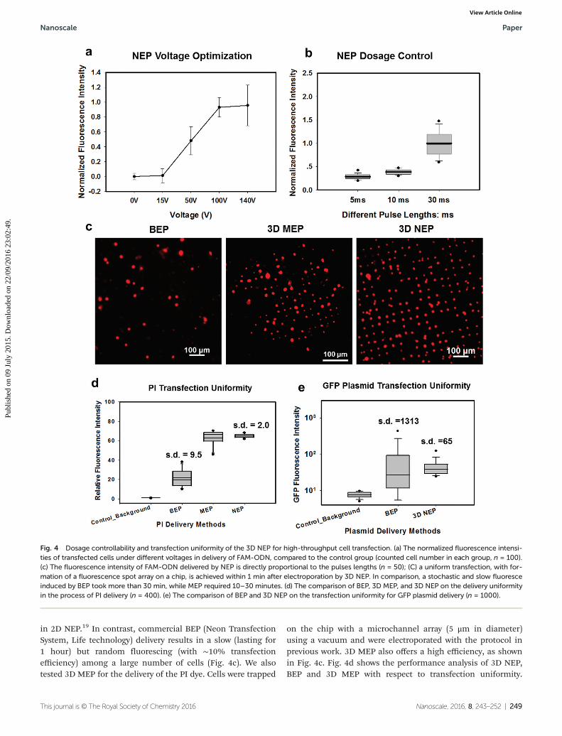
in 2D NEP.19 In contrast, commercial BEP (Neon TransfectionSystem, Life technology) delivery results in a slow (lasting for1 hour) but random fluorescing (with ∼10% transfectionefficiency) among a large number of cells (Fig. 4c). We alsotested 3D MEP for the delivery of the PI dye. Cells were trapped
on the chip with a microchannel array (5 μm in diameter)using a vacuum and were electroporated with the protocol inprevious work. 3D MEP also offers a high efficiency, as shownin Fig. 4c. Fig. 4d shows the performance analysis of 3D NEP,BEP and 3D MEP with respect to transfection uniformity.
Fig. 4 Dosage controllability and transfection uniformity of the 3D NEP for high-throughput cell transfection. (a) The normalized fluorescence intensi-ties of transfected cells under different voltages in delivery of FAM-ODN, compared to the control group (counted cell number in each group, n = 100).(c) The fluorescence intensity of FAM-ODN delivered by NEP is directly proportional to the pulses lengths (n = 50); (C) a uniform transfection, with for-mation of a fluorescence spot array on a chip, is achieved within 1 min after electroporation by 3D NEP. In comparison, a stochastic and slow fluoresceinduced by BEP took more than 30 min, while MEP required 10–30 minutes. (d) The comparison of BEP, 3D MEP, and 3D NEP on the delivery uniformityin the process of PI delivery (n = 400). (e) The comparison of BEP and 3D NEP on the transfection uniformity for GFP plasmid delivery (n = 1000).
Nanoscale Paper
This journal is © The Royal Society of Chemistry 2016 Nanoscale, 2016, 8, 243–252 | 249
Publ
ishe
d on
09
July
201
5. D
ownl
oade
d on
22/
09/2
016
23:0
2:49
. View Article Online

In each group, the fluorescence intensities of 400 randomly-picked individual cells are counted. 3D NEP shows signifi-cantly higher transfection uniformity (s.d. = 2) than that ofBEP (s.d. = 9.5) and 3D MEP (s.d. = 8.1). Note that at low meanintensity, 3D MEP works well for intracellular delivery of smallmolecules too. We further investigated the efficacy of BEP andMEP for the delivery of large molecular weight plasmids(pmaxGFP, 3.5 kbp) compared to NEP. Fig. 4e analyzes theGFP fluorescence intensities of 1000 cells in BEP and NEPgroups. 3D NEP has 20-fold better uniformity than BEP onplasmid delivery (s.d = 65 vs. s.d. = 1313), implying thesuperior performance of NEP in regard to transfection uni-formity when attempting to transfect cells with large mole-cules. NEP also showed significantly higher efficiency forplasmid delivery as compared to MEP platforms. GFP fluo-
rescence was not observed in 3D MEP experiments. When theapplied voltage was increased to 10 V, however, all cells loadedon the micro-pores were lysed due to joule heating, consistentwith the previous work on MEP.39,40
Large weight plasmids delivery in primary cells
We further explored the outcomes specific to the delivery oflarge molecular weight plasmids (OCT-4, SOX2, KCL-1, andMYC transcription factors, OSKM encoded on a pCAG plasmidbackbone, with 13 kbp) into the primary cells (mouse embryo-nic fibroblasts) on the 3D NEP platform. The plasmid labelledwith YOYO-1 dye, is capable of improving the fluorescenceintensity 1000-fold once it binds with dsDNA in either thecytosol or nucleus.36 We observed a strong YOYO-1 fluorescencesignal co-localized with the cells 1 min after NEP (Fig. 5a),
Fig. 5 Delivery of MEFs with large molecular weight cargos (13 kbp OSKM plasmid labelled with YOYO-1 dye) using a 3D NEP platform and BEP. (a)The images merged with YOYO-1 green fluorescence and phase contrast show that the delivery efficiency of 3D NEP is significantly higher than thatof BEP (the first panel). The zoom-in of individual cells demonstrates that cells transfected by NEP are still alive, with typical MEF morphologies,while most cells delivered by BEP show spherical morphologies and detach from dishes, indicating cell death (the second panel). (b) Statistics of cellviability between NEP and BEP (n = 100). (c) The transfection uniformity of NEP as compared to BEP, according to the internalized YOYO-1 fluor-escence (n = 100). (d) Successful expression of OSKM transcriptional factors after 3D NEP. The RFP fluorescence (reporter gene encoded on OSKMplasmid) was observed 24 h after NEP, indicating the successful translation and transcription of OSKM factors. **: p < 0.01.
Paper Nanoscale
250 | Nanoscale, 2016, 8, 243–252 This journal is © The Royal Society of Chemistry 2016
Publ
ishe
d on
09
July
201
5. D
ownl
oade
d on
22/
09/2
016
23:0
2:49
. View Article Online

indicating the internalization of the plasmid. Fig. 5a alsodemonstrates that NEP provides significantly higher efficiencythan BEP when delivering such large molecular weight cargos(∼10% vs. <1%). For NEP, it should be noted that as men-tioned earlier, only cells seated on nanopores can be trans-fected, which is why the seemingly low transfection efficiencyof 10%, as all cells loaded on the chips were counted ratherthan only those seated on nanopores. A cell manipulationtechnique for high-throughput cell trapping on a 3D NEP chipis under investigation now, which would realize efficient cell-array trapping, allowing a better alignment with the nanochan-nel array. If we count only cells localized on the nanopores,the transfection efficiency would be at ∼90%. The result ofextremely low-efficiency obtained by BEP was consistent withprevious work for OSKM plasmid delivery.41 We also evaluatedthe cell viability after electroporation. In the NEP group, 90%of transfected cells are still alive (Fig. 5b), attached andshowed typical fibroblast morphologies 24 hours after electro-poration (Fig. 5a). In comparison, in the BEP group, only 9%cells are still considered surviving while 91% cells displayshrunken, spherical features and have detached from the cellculture dish, a typical behaviour of dead or dying cells(Fig. 5a). The reason for negligible cell damage with NEP hasbeen discussed above and in previous work.19 The unique cell-nanochannel configuration shields the majority of potentialdrops, allowing a safe but sufficient voltage potential to poratecells. The extremely low efficiency of BEP supports the fact thatBEP is a diffusion based process where without additional pro-pulsion, the difficulty of cross-membrane transport is toogreat. This also suggests that for a successful BEP, an increasein the applied voltage would be required in order to improvedelivery efficiency. However, this would cause irreversible elec-troporation to occur, leading to permanent cell damage.38 Wealso compared the fluorescence intensities between twogroups, and NEP consistently shows significantly better uni-formity (s.d. = 4306) than BEP (s.d. = 12 347) (Fig. 5c). TheOSKM plasmid was also cloned with a reporter gene (RFP) toverify if the plasmids were transcribed and translated in livingcells. Fig. 5d shows RFP (red fluorescence) observed 24 hoursafter NEP, indicating the successful transcription of the OSKMfactors. All cells showing RFP can be co-localized with thoseemitting YOYO-1 fluorescence, demonstrating that the RFPsignal is real and reliable. However, only a portion of deliveredcells (based on YOYO-1) showed the RFP signal, implyingOSKM factors were not suitably expressed in some cells. Ourhypothesis is that the current OSKM plasmid is an integrativebackbone cloned with five functional genes (OCT-4, SOX2,KCL-1, MYC, and RFP), which increases the difficulties ofcorrect expression in the nucleus.
Conclusions
The manipulation of cellular behaviour and programming mayprove essential to the future of clinical medicine and thera-peutics. The development of a highly reliable, controllable,
and low-cost system is ideal to allow for a smooth transitionfrom research to clinical medicine. BEP, while commerciallyavailable and easily performed, is extremely detrimental to cellfunction and longevity. While BEP allows for high-throughput,it is unable to achieve high cell viability and any dosagecontrol. MEP improves upon this system by being able toachieve high-throughput and higher cell viability, but it is stillunable to achieve good dosage control and uniform transfec-tion and to deliver large molecular weight cargos. The 3D NEPsystem demonstrated here allows for high-throughput celltransfection with high cell viability, dosage control, and highuniformity. These features promote the qualities of gene deliv-ery and transfection in gene therapy, adoptive immunotherapyand cell reprogramming. This platform also offers highefficiency and cell viability in delivering cells with very largemolecular weight cargos (e.g. 13 kbp OSKM plasmids) whichcannot be achieved with comparable outcomes by either MEPor BEP. The 3D NEP system used in this experiment canhandle 40 000 cells on a single chip with 1 cm2 area. If a largernumber of cells are required, the demonstrated approach canbe readily scaled up to deal with millions of cells per wafer.
Author contribution statement
W.L. and L.J.L. conceived and designed the experiments. L.C.,P.B., D.G.-P., and V.M. conducted 3D NEP chip fabrication. L.C., F.C., T.K. assembled the 3D NEP system and conducted 3DNEP experiment. Z.Y. and C.-L.C. assisted with cell culture andbio-statistics. P.B. performed the simulation. L.C. and P.B.made the data analysis and wrote the paper. W.L. and L.J.L.revised and finalized the paper.
Acknowledgements
The authors are grateful to Mark Brenner from ECE Depart-ment at OSU for providing technical support of DRIE tech-nique, and Cheng Kang from the Department of Pharmacologyfor providing cells. The authors thank the National ScienceFoundation (EEC-0914790) for supporting this study.
Notes and references
1 M. Costa, M. Dottori, K. Sourris, P. Jamshidi, T. Hatzistavrou,R. Davis, L. Azzola, S. Jackson, S. M. Lim, M. Pera,A. G. Elefanty and E. G. Stanley, Nat. Protoc., 2007, 2, 792–796.
2 K. Kaji, K. Norrby, A. Paca, M. Mileikovsky, P. Mohseni andK. Woltjen, Nature, 2009, 458, 771–U112.
3 L. Naldini, U. Blomer, P. Gallay, D. Ory, R. Mulligan,F. H. Gage, I. M. Verma and D. Trono, Science, 1996, 272,263–267.
4 R. King, Methods Mol. Biol., 2004, 245, 167–174.5 H. Chantrenne, Nature, 1977, 269, 202–202.6 S. Mehier-Humbert and R. H. Guy, Adv. Drug Delivery Rev.,
2005, 57, 733–753.
Nanoscale Paper
This journal is © The Royal Society of Chemistry 2016 Nanoscale, 2016, 8, 243–252 | 251
Publ
ishe
d on
09
July
201
5. D
ownl
oade
d on
22/
09/2
016
23:0
2:49
. View Article Online

7 M. Zernicka-Goetz, Nature, 2000, 405, 733–733.8 U. K. Tirlapur and K. Konig, Nature, 2002, 418, 290–291.9 P. Chakravarty, W. Qian, M. A. El-Sayed and M. R. Prausnitz,
Nat. Nanotechnol., 2010, 5, 607–611.10 E. Kang, J. Ryoo, G. S. Jeong, Y. Y. Choi, S. M. Jeong, J. Ju,
S. Chung, S. Takayama and S. H. Lee, Adv. Mater., 2013, 25,2167–2173.
11 M. R. Prausnitz, V. G. Bose, R. Langer and J. C. Weaver,Proc. Natl. Acad. Sci. U. S. A., 1993, 90, 10504–10508.
12 F. Liu, S. Heston, L. M. Shollenberger, B. Sun, M. Mickle,M. Lovell and L. Huang, J. Gene. Med., 2006, 8, 353–361.
13 S. Y. Ho and G. S. Mittal, Crit. Rev. Biotechnol., 1996, 16,349–362.
14 L. H. Li, M. Wood, R. Shivakumar, S. Feller, S. Wang,V. Singh, J. Holaday, J. Fratantoni and L. N. Liu, Blood,2001, 98, 425a–425a.
15 R. P. Joshi and K. H. Schoenbach, Phys. Rev. E: Stat. Phys.,Plasmas, Fluids, Relat. Interdiscip. Top., 2002, 66.
16 Y. C. Wu, T. H. Wu, D. L. Clemens, B. Y. Lee, X. Wen,M. A. Horwitz, M. A. Teitell and P. Y. Chiou, Nat. Methods,2015, 12(4), 439–444.
17 B. Marrero and R. Heller, Biomaterials, 2012, 33, 3036–3046.
18 E. G. Guignet and T. Meyer, Nat. Methods, 2008, 5, 393–395.
19 P. E. Boukany, A. Morss, W. C. Liao, B. Henslee, H. C. Jung,X. L. Zhang, B. Yu, X. M. Wang, Y. Wu, L. Li, K. L. Gao,X. Hu, X. Zhao, O. Hemminger, W. Lu, G. P. Lafyatis andL. J. Lee, Nat. Nanotechnol., 2011, 6, 747–754.
20 W. Kang, J. P. Giraldo-Vela, S. S. P. Nathamgari, T. McGuire,R. L. McNaughton, J. A. Kessler and H. D. Espinosa, LabChip, 2014, 14, 4486–4495.
21 T. Geng and C. Lu, Lab Chip, 2013, 13, 3803–3821.22 T. Geng, Y. Zhan, J. Wang and C. Lu, Nat. Protoc., 2011, 6,
1192–1208.23 L. Yan, J. Zhang, C. S. Lee and X. Chen, Small, 2014, 10,
4487–4504.24 K. L. Gao, L. Li, L. N. He, K. Hinkle, Y. Wu, J. Y. Ma,
L. Q. Chang, X. Zhao, D. G. Perez, S. Eckardt, J. Mclaughlin,
B. Y. Liu, D. F. Farson and L. J. Lee, Small, 2014, 10, 1015–1023.
25 W. M. Kang, F. Yavari, M. Minary-Jolandan, J. P. Giraldo-Vela, A. Safi, R. L. McNaughton, V. Parpoil andH. D. Espinosa, Nano Lett., 2013, 13, 2448–2457.
26 C. Xie, Z. Lin, L. Hanson, Y. Cui and B. Cui, Nat. Nanotech-nol., 2012, 7, 185–190.
27 X. Xie, A. M. Xu, S. Leal-Ortiz, Y. H. Cao, C. C. Garner andN. A. Melosh, ACS Nano, 2013, 7, 4351–4358.
28 Z. Z. Fei, S. N. Wang, Y. B. Xie, B. E. Henslee, C. G. Koh andL. J. Lee, Anal. Chem., 2007, 79, 5719–5722.
29 Z. Z. Fei, X. Hu, H. W. Choi, S. N. Wang, D. Farson andL. J. Lee, Anal. Chem., 2010, 82, 353–358.
30 L. Chang, M. Howdyshell, W. C. Liao, C. L. Chiang,D. Gallego-Perez, Z. Yang, W. Lu, J. C. Byrd, N. Muthusamy,L. J. Lee and R. Sooryakumar, Small, 2015, 11, 1818–1828.
31 Y. C. Liu, W. Y. Lin, Y. R. Jhang, S. H. Huang, C. P. Wu andH. T. Wu, Appl. Biochem. Biotechnol., 2011, 164, 1172–1182.
32 T. Kotnik, F. Bobanovic and D. Miklavcic, Bioelectrochem.Bioenerg., 1997, 43, 285–291.
33 Y. G. Man, T. Vinh, C. Zhao, A. Walker and R. Barner, Mod.Pathol., 2005, 18, 42a.
34 G. Sersa, T. Jarm, T. Kotnik, A. Coer, M. Podkrajsek,M. Sentjurc, D. Miklavcic, M. Kadivec, S. Kranjc, A. Secerovand M. Cemazar, Br. J. Cancer, 2008, 98, 388–398.
35 S. Movahed and D. Q. Li, J. Colloid Interface Sci., 2012, 369,442–452.
36 C. Gupta, W. C. Liao, D. Gallego-Perez, C. E. Castro andL. J. Lee, Biomicrofluidics, 2014, 8.
37 S. I. E. Lin, Adv. Mater. Res., 2012, 586, 421–429.38 A. Golberg and M. L. Yarmush, IEEE Trans. BioMed. Eng.,
2013, 60, 707–714.39 Y. Huang and B. Rubinsky, Sens. Actuators, A, 2001, 89,
242–249.40 A. Valero, J. N. Post, J. W. van Nieuwkasteele, P. M. Ter
Braak, W. Kruijer and A. van den Berg, Lab Chip, 2008, 8,62–67.
41 M. C. N. Marchetto, G. W. Yeo, O. Kainohana, M. Marsala,F. H. Gage and A. R. Muotri, PLoS One, 2009, 4.
Paper Nanoscale
252 | Nanoscale, 2016, 8, 243–252 This journal is © The Royal Society of Chemistry 2016
Publ
ishe
d on
09
July
201
5. D
ownl
oade
d on
22/
09/2
016
23:0
2:49
. View Article Online

![Fabrication and Measurement of a Suspended Nanochannel ... · resolution in References [4–6]. However, in these cases, optical detection techniques were used, making more difficult](https://img.pdfslide.us/doc/110x75/5f68c60abdf53b60d4317a73/fabrication-and-measurement-of-a-suspended-nanochannel-resolution-in-references.jpg)