Embed Size (px)
Citation preview

3D integrated and digitally read-out
solid-state photo-multiplier –proposal for wafer scale focal planes
Grzegorz (Gregory) DeptuchJuan Estrada
Fermilab
KICP workshop: "Imaging the Extreme Universe: Solid-state cameras for Astroparticle Physics"
9-10 May, 2013
SILVACO process simulatiom
2 KICP Workshop, 9-10 May, 2013
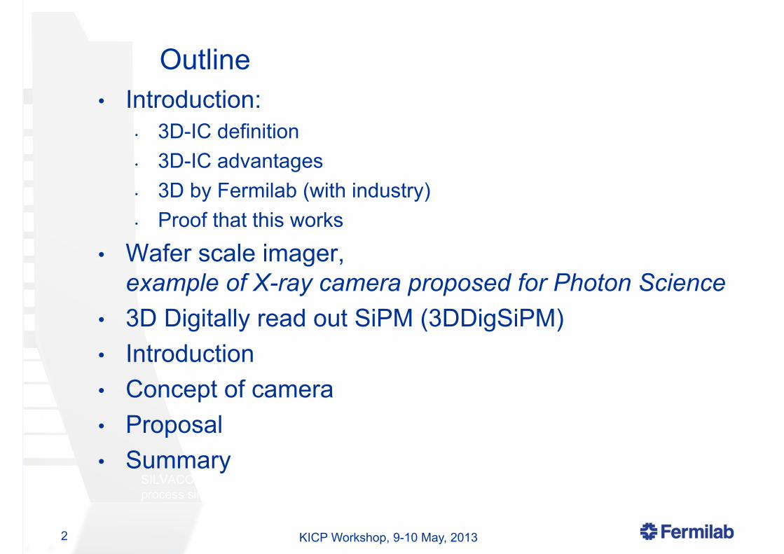
Outline• Introduction:
• 3D-IC definition• 3D-IC advantages• 3D by Fermilab (with industry)• Proof that this works
• Wafer scale imager,example of X-ray camera proposed for Photon Science
• 3D Digitally read out SiPM (3DDigSiPM)• Introduction • Concept of camera• Proposal• Summary

SILVACO process simulatiom
3 KICP Workshop, 9-10 May, 2013
• Through Silicon Vias (TSV): small diameter vertical connectivity (not only to build electronic chips but also for attaching detectors to readouts)
• Bonding: Oxide-, polymer-, metal-, or adhesive strengthened- (W-W, C-W or C-C)• Wafer thinning: aggressive and ultra-precise• Back-side processing: metallization and patterning
A chip in three-dimensional integrated circuit (3D-IC) technology is composed of two or more layers of active electronic components using horizontal intra-tierand vertical inter-tier connectivity routing
MIT-LL 3D-IC processFDSOI oxide-
oxide bonding
Face-Face
Back-Face
Face-Face
Tezzaron 3D-ICbulk CMOS Cu-Cu
thermocompressionor DBI bonding TS Vias
(φ=1μm)
2 technology options explored
3D-IC: definition

SILVACO process simulatiom
4 KICP Workshop, 9-10 May, 2013
• 3D-IC offers a transformational change to address current roadblocks in advancing fine-grained detector, and with in-situ processing.
• 3D ROICs - complete separation of digital activity from low-noise
analog parts• 3D ROICs - uniform distribution
of power supply and I/O pads on the back side
• ROICs can be integrated with sensors without bump-bonds
Strategic direction: 4 side buttable, dead-area-free detectors
3D-IC: benefits
SILVACO process simulatiom
5 KICP Workshop, 9-10 May, 2013
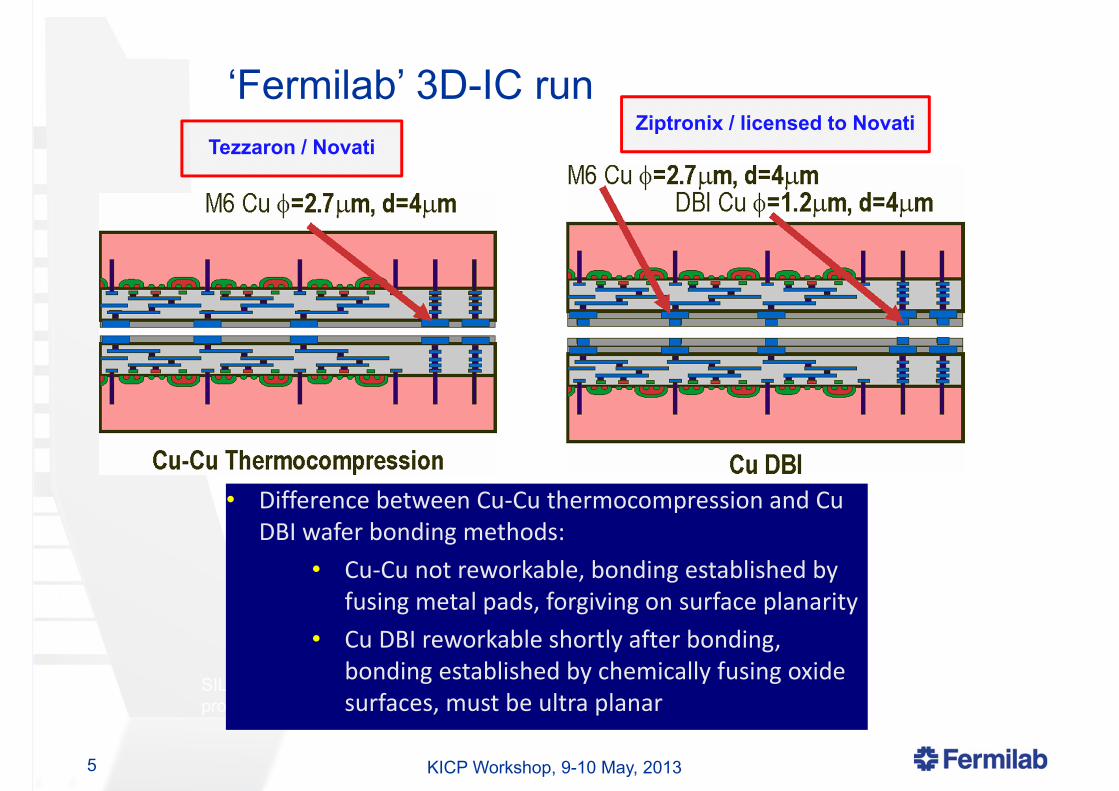
• Difference between Cu-Cu thermocompression and Cu DBI wafer bonding methods:
• Cu-Cu not reworkable, bonding established by fusing metal pads, forgiving on surface planarity
• Cu DBI reworkable shortly after bonding, bonding established by chemically fusing oxide surfaces, must be ultra planar
‘Fermilab’ 3D-IC runTezzaron / Novati
Ziptronix / licensed to Novati

SILVACO process simulatiom
6 KICP Workshop, 9-10 May, 2013
• Initial (small) efforts started with MIT-LL 3D process in 2006 (DARPA 3-tier 3D run):• stimulated great interest among the detector
community worldwide and move to Tezzaron/GF
• 3D-IC Consortium established in late 2008, now 17 members; 6 countries: USA, Italy, France, Germany, Poland, Canada) + Tezzaron – various goals among members,activities going at slower pace but progressing
• Fermilab organized first 3D-IC MPW run for HEP• Designs in: 05/2009; Chartered (GF) 130nm
• Fermilab had a role of silicon broker • Many challenges in working with cutting edge technology; to
name some: design mistakes, incompatibility of software tools (Tezzaron not Cadence), lack of 3D oriented verification, handling of databases >10GB, shifting GF requirements (DRC), changing personnel at GF, etc.
• MPW frame accepted for fab in 03/2010
LEFT (bottom)chips
Right (top)chips
‘Fermilab’ 3D-IC run
130nm GF/Tezzaron wafer - FNAL MPW before 3D bonding; single mask set used to fabricate
top and bottom tier chips on the same wafer;Bonding by flipping wafers over symmetry line

SILVACO process simulatiom
7 KICP Workshop, 9-10 May, 2013
chips with pads on front side to a sensor DBI
or stud bonding
chips with pads distributedon whole back surface
‘Fermilab’ 3D-IC run
VIPIC1 (3D chip for photon science XPCS at BNL)64x64 pixel @ 80μm pitch
Fabricated and tested …
SEM image of W TSVs providing contact to back-side AL pad on VIPIC1
sparsified readout inter-tier communication
noise @ nominal bias in input transistor and with CSA replica off
for gain from measurements

8
Wafer scale imagers using 3D-ICNewly developed proposal of a wafer-size camera for
the Advanced Photon Source at ANL
KICP Workshop, 9-10 May, 2013
Key features • Seamless, wafer scale (6” or 8”)
imaging (focal) plane for X-ray science – single piece camera,
• 150×150 μm2 - 100×100 μm2 pixels,
• SiPCB technology for tapered pitch adaptation and sturdy support,
• Fast front ends, DR 1 photons – 105
photons / pixel @ 8keV (up to 40pC)• Light and simple form,

9
3DDigSiPM - introduction
KICP Workshop, 9-10 May, 2013
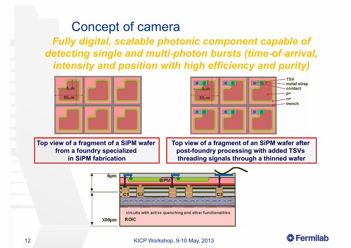
Fully digital, scalable photonic component capable of detecting single and multi‐photon bursts (time‐of‐arrival,
intensity and position with high efficiency and purity)
What can an array of digital SiPMs do?
E. Charbon, FEE 2011Bergamo, Italy
- act on individual cells to disable noisy ones and fine tune parameters (gain variations not important any more)

10
What can 3D-integrated digital SiPMs do?
KICP Workshop, 9-10 May, 2013
SPAD in 2D
SPAD/SiPM in 3D-IC technology
• Process for sensors (SiPM cells) and circuits chosen to optimize both; DCR <0.1Hz/μm2
• Fill factor highest possible to achieve!• Entrance window can be as thin as tens of
nanometers – for sensitivity in BLUE!• Use of 3D-integration techniques allow building
large area seamlessly tiled devices• Electronics may have many variants!
• IC process to get low DCR and be suitable for highly packed circuits is problematic; SPADs in dedicated technology: 0.1~1Hz/μm2,CMOS SPADs: 1~10Hz/μm2
• Poor fill factor, more electronics per pixel = less sensitive area!
3D SiPM
11
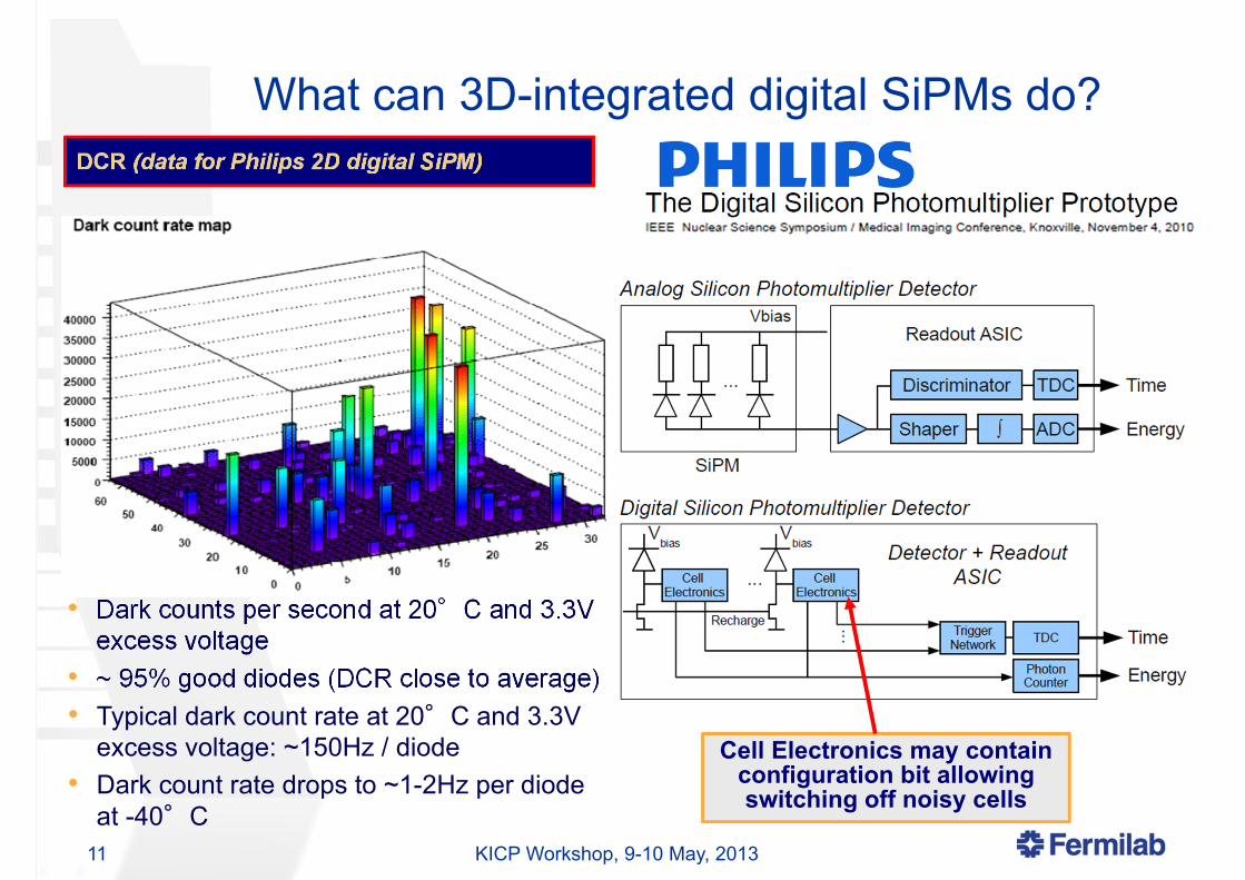
What can 3D-integrated digital SiPMs do?
KICP Workshop, 9-10 May, 2013
DCR (data for Philips 2D digital SiPM)
• Dark counts per second at 20°C and 3.3V excess voltage
• ~ 95% good diodes (DCR close to average)• Typical dark count rate at 20°C and 3.3V
excess voltage: ~150Hz / diode• Dark count rate drops to ~1-2Hz per diode
at -40°C
Cell Electronics may contain configuration bit allowing switching off noisy cells
12 KICP Workshop, 9-10 May, 2013
Fully digital, scalable photonic component capable of detecting single and multi‐photon bursts (time‐of‐arrival,
intensity and position with high efficiency and purity)
Top view of a fragment of a SiPM wafer from a foundry specialized
in SiPM fabrication
Top view of a fragment of an SiPM wafer after post-foundry processing with added TSVs threading signals through a thinned wafer
Concept of camera

13
Concept of camera
KICP Workshop, 9-10 May, 2013
SiPM
ASIC
SiPCB
Add another component:SiPCB and you obtain
Large-scale-self-supporting single photona sens. camera
14 KICP Workshop, 9-10 May, 2013
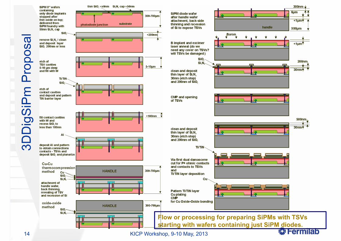
Flow or processing for preparing SiPMs with TSVs starting with wafers containing just SiPM diodes.

15
3DDigSiPM - proposal
KICP Workshop, 9-10 May, 2013
• Using 3D-IC technology decouples tasks – optimization: process for sensor-SiPM and process for ASIC at uncompromised FF,
• Cell circuitry may have many flavors and various functionalities
• Act on individual cells to disable noisy ones and fine tune parameters (gain variations not important any more)
• Every SiPM diode can be controlled individually; e.g. active quenching to eliminate after-pulsing
Active quenching
16
3DDigSiPM - proposal
KICP Workshop, 9-10 May, 2013
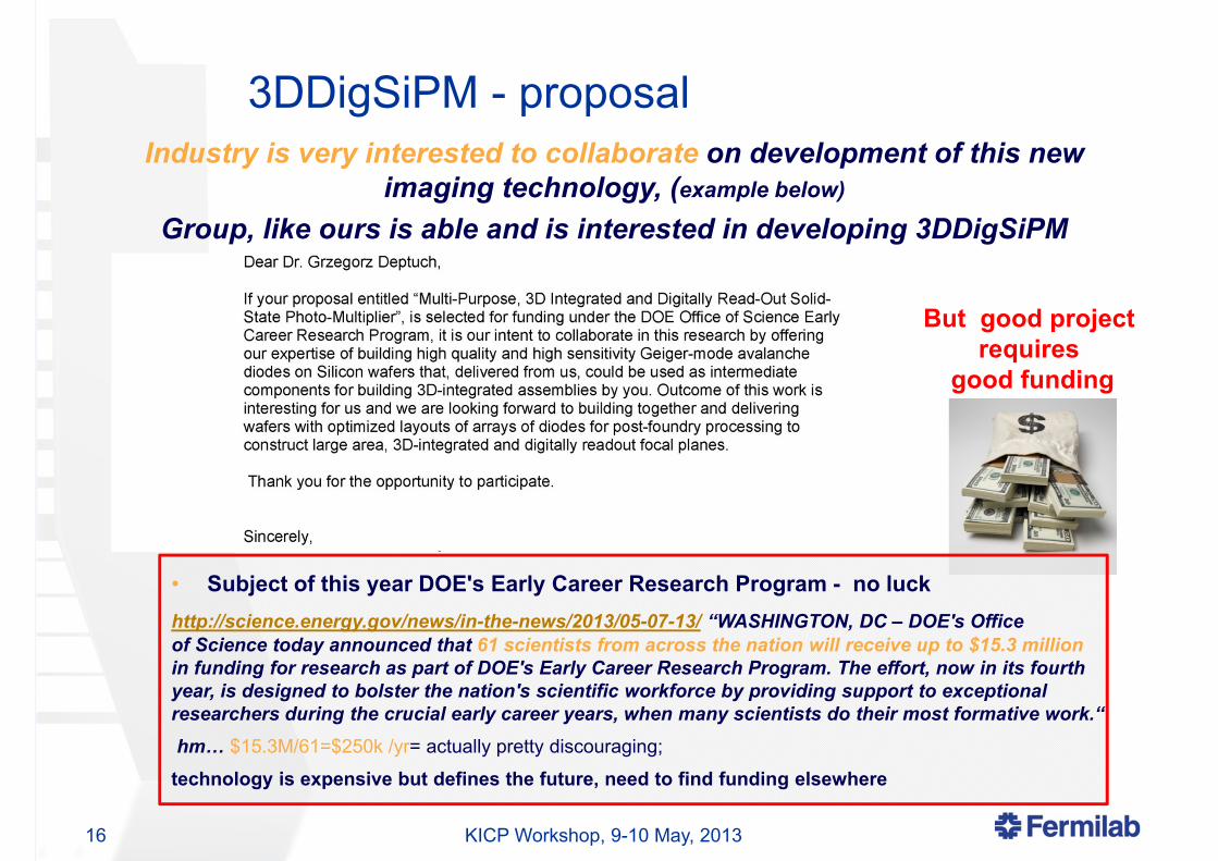
Industry is very interested to collaborate on development of this new imaging technology, (example below)
Group, like ours is able and is interested in developing 3DDigSiPM
• Subject of this year DOE's Early Career Research Program - no luckhttp://science.energy.gov/news/in-the-news/2013/05-07-13/ “WASHINGTON, DC – DOE's Office of Science today announced that 61 scientists from across the nation will receive up to $15.3 millionin funding for research as part of DOE's Early Career Research Program. The effort, now in its fourth year, is designed to bolster the nation's scientific workforce by providing support to exceptional researchers during the crucial early career years, when many scientists do their most formative work.“hm… $15.3M/61=$250k /yr= actually pretty discouraging;
technology is expensive but defines the future, need to find funding elsewhere
But good project requires
good funding
17
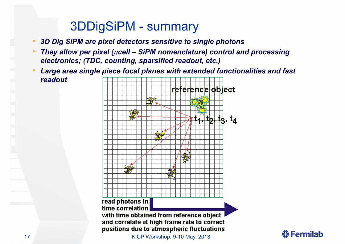
3DDigSiPM - summary
KICP Workshop, 9-10 May, 2013
• 3D Dig SiPM are pixel detectors sensitive to single photons• They allow per pixel (μcell – SiPM nomenclature) control and processing
electronics; (TDC, counting, sparsified readout, etc.) • Large area single piece focal planes with extended functionalities and fast
readout