Embed Size (px)
Citation preview

IEEE 64th ECTC – Orlando, FL, USA May 27–30, 2014
Add Company Logo Here
3D-ICs: Advances in the Industry
Suresh Ramalingam
Advanced Packaging, Xilinx
2100 Logic Drive, San Jose, 95124
2014 CPMT Seminar Latest Advances in Organic Interposers

2 IEEE 64th ECTC – Orlando, FL, USA May 27 – 30, 2014 Suresh Ramalingam
3D IC Background
3D IC Technology Development
Summary
Acknowledgements
Outline
Stacked Silicon Interconnect Technology refers to Xilinx 3D solutions

3 IEEE 64th ECTC – Orlando, FL, USA May 27 – 30, 2014 Suresh Ramalingam
3D IC Background

4 IEEE 64th ECTC – Orlando, FL, USA May 27 – 30, 2014 Suresh Ramalingam
Technical Challenges & Costs Are Growing
Process Technology Path Below 10nm is unclear
Cost Reduction Slowing from Complexity / Investment Increases
Cost Per Wafer & Cost Per Gate Deviating from Historical Reduction

5 IEEE 64th ECTC – Orlando, FL, USA May 27 – 30, 2014 Suresh Ramalingam
3DIC Extends Moore’s Law
Cost Comparison: Monolithic vs. Multi-Die
Die Area
Die
Co
st
Monolithic
Multi-Die
“Moore’s Law is Really About Economics” – Gordon Moore

6 IEEE 64th ECTC – Orlando, FL, USA May 27 – 30, 2014 Suresh Ramalingam
Design Rule Comparison
Design Rules for Die to
Die interconnection
MCM
(Substrate)
MCM with
Silicon Bridge
Silicon
Interposer
(65 nm BEOL)
WLFO /
Organic
Interposer
Minimum Bump pitch (um) 150 (C4) 150 (C4)
40 (u-bump) bridge
< 40 (u-bump) 40 um RDL pad
pitch
Via size / pad size (um) 60 / 90 0.4 / 0.7 0.4 / 0.7 10/30
Minimum Line & Space (um) 15 / 15 0.4 / 0.4 0.4 / 0.4 3 / 3
Metal thickness (um) 10 1 1 2-5
Dielectric thickness (um) 30 1 1 < 5
# of die-to-die connections per
layer + GND shield layer (2L)
100’s 10,000’s 10,000’s 1000’s
Minimum die to die spacing (um) 4000 Bridge ~ 2500 150 < 250
# of High density layers feasible Not a limitation Not a limitation Not a limitation 1-3L layers
Die Sizes for assembly and # of
assemblies
Not a concern Size & # limitation? Not a concern Size limitation?
Xilinx pursuing Silicon Interposer for design rule
density, BW and lower power – e.g. die partition

7 IEEE 64th ECTC – Orlando, FL, USA May 27 – 30, 2014 Suresh Ramalingam
Supply Chain
TSV Si
Interposer
TSV Si
Interposer
Chip-on-Wafer
Bonding (1)
FPGA (1)
Memory (2)
Logic IP (3)
Thinning/
C4/Sorting
Packaging on
substrate
Final Test &
Shipment
TSMC CoWoSTM
UMC
SPIL
Interposer Thinning/
C4/Sorting
KGI die
reconfiguration
*Re-usable cavity wafer
De-carrier &
Dicing
Packaging on
substrate
uBump/Sort
uBump/Sort
uBump/Sort
TSMC CoWoS in production
Readying UMC/SPIL as additional source. Completed technology qualification
KGD (1~3)
chip stacking

8 IEEE 64th ECTC – Orlando, FL, USA May 27 – 30, 2014 Suresh Ramalingam
Virtex-7 2000T
Interposer Area: ~775 mm2
Population: ~6.8 Billion Transistors
Chips: 5
Earth
Area: ~500 Million km2
Population: ~6.8 Billion People
Oceans: 5
Xilinx 28nm 3DIC – Huge Leap in Innovation
136 Patents Awarded Worldwide
226 Pending Applications Worldwide

9 IEEE 64th ECTC – Orlando, FL, USA May 27 – 30, 2014 Suresh Ramalingam
3D IC Technology Development

10 IEEE 64th ECTC – Orlando, FL, USA May 27 – 30, 2014 Suresh Ramalingam Page 10
CoWoS Technology
– Top dies are attached to full-thickness interposer wafers thus getting around the thin
interposer warpage and poor micro-bump joining problem
Reconfigurable CoW (rCoW) Technology
– Xilinx patent issued worldwide (US/TWN/CN/EU/IND/JPN/KR)
– Release layer approach that withstands reflow & maintains low warpage
Warpage control Keep warpage below <10um over entire temp range
CoS
CoWoS rCoW
Critical Challenge: Warpage Control
11 IEEE 64th ECTC – Orlando, FL, USA May 27 – 30, 2014 Suresh Ramalingam
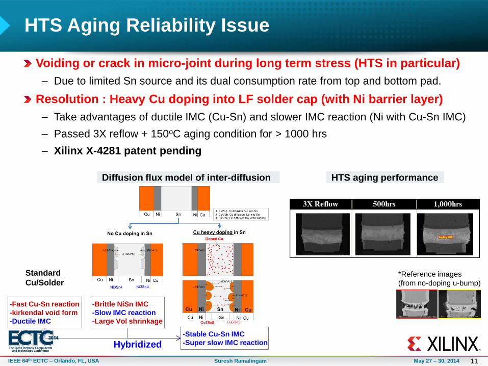
HTS Aging Reliability Issue
Voiding or crack in micro-joint during long term stress (HTS in particular)
– Due to limited Sn source and its dual consumption rate from top and bottom pad.
Resolution : Heavy Cu doping into LF solder cap (with Ni barrier layer)
– Take advantages of ductile IMC (Cu-Sn) and slower IMC reaction (Ni with Cu-Sn IMC)
– Passed 3X reflow + 150oC aging condition for > 1000 hrs
– Xilinx X-4281 patent pending
-Stable Cu-Sn IMC
-Super slow IMC reaction
Standard
Cu/Solder
Diffusion flux model of inter-diffusion HTS aging performance
-Fast Cu-Sn reaction
-kirkendal void form
-Ductile IMC
-Brittle NiSn IMC
-Slow IMC reaction
-Large Vol shrinkage
Hybridized
*Reference images
(from no-doping u-bump)
12 IEEE 64th ECTC – Orlando, FL, USA May 27 – 30, 2014 Suresh Ramalingam
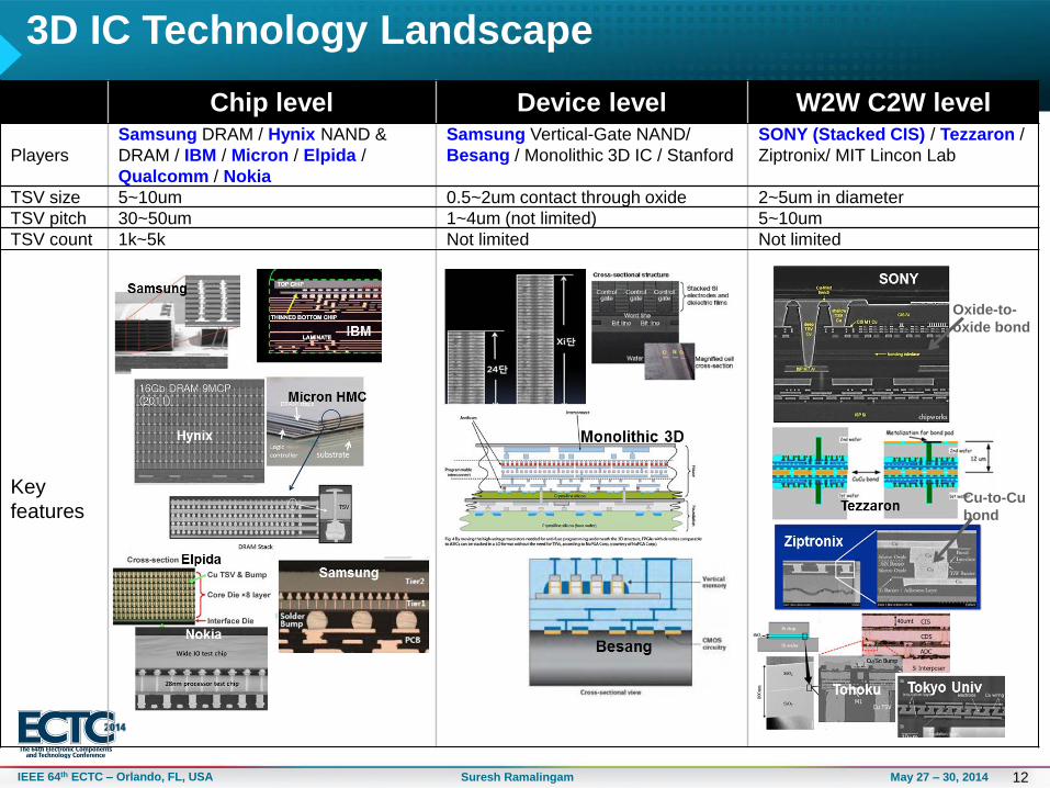
Chip level Device level W2W C2W level
Players
Samsung DRAM / Hynix NAND &
DRAM / IBM / Micron / Elpida /
Qualcomm / Nokia
Samsung Vertical-Gate NAND/
Besang / Monolithic 3D IC / Stanford
SONY (Stacked CIS) / Tezzaron /
Ziptronix/ MIT Lincon Lab
TSV size 5~10um 0.5~2um contact through oxide 2~5um in diameter
TSV pitch 30~50um 1~4um (not limited) 5~10um
TSV count 1k~5k Not limited Not limited
Key
features
3D IC Technology Landscape
Oxide-to-
oxide bond
Cu-to-Cu
bond

13 IEEE 64th ECTC – Orlando, FL, USA May 27 – 30, 2014 Suresh Ramalingam
Economic and technology forces
are aligned to enable 2.5D/3D stacking
The “end game” will see three distinct
technologies: Logic, Memory, Analog
TSV and 3D stacking already deployed in
Smartphones, High end FPGAs & Servers
Page 13
Summary
Analog Logic
Mem
Package

14 IEEE 64th ECTC – Orlando, FL, USA May 27 – 30, 2014 Suresh Ramalingam
Xilinx
– R&D, NPI & Operation Teams
Partners
– TSMC R&D and Production Teams for FPGA, CoWoS
– UMC for Interposer
– SPIL R&D for MEOL and Advanced Packaging
– Fujitsu Interconnect Technology for High Speed Substrates
Acknowledgements


![“Where ICs are in the IEEE”ewh.ieee.org/r5/dallas/sscs/slides/20120829dallas.pdf · Part of IEEE with 400,000 members . ... enc gate # ... [El-Chammas, VLSI 2010] CAL V lo V hi](https://img.pdfslide.us/doc/110x75/5b0af3717f8b9a99488d0076/where-ics-are-in-the-ieeeewhieeeorgr5dallassscsslides-of-ieee-with.jpg)