Embed Size (px)
Citation preview
General rights Copyright and moral rights for the publications made accessible in the public portal are retained by the authors and/or other copyright owners and it is a condition of accessing publications that users recognise and abide by the legal requirements associated with these rights.
• Users may download and print one copy of any publication from the public portal for the purpose of private study or research. • You may not further distribute the material or use it for any profit-making activity or commercial gain • You may freely distribute the URL identifying the publication in the public portal
If you believe that this document breaches copyright please contact us providing details, and we will remove access to the work immediately and investigate your claim.
Downloaded from orbit.dtu.dk on: Aug 14, 2018
3D continuum phonon model for group-IV 2D materials
Willatzen, Morten; Lew Yan Voon, Lok C.; Gandi, Appala Naidu; Schwingenschlogl, Udo
Published in:Beilstein Journal of Nanotechnology
Link to article, DOI:10.3762/bjnano.8.136
Publication date:2017
Document VersionPublisher's PDF, also known as Version of record
Link back to DTU Orbit
Citation (APA):Willatzen, M., Lew Yan Voon, L. C., Gandi, A. N., & Schwingenschlogl, U. (2017). 3D continuum phonon modelfor group-IV 2D materials. Beilstein Journal of Nanotechnology, 8(1), 1345-1356. DOI: 10.3762/bjnano.8.136

1345
3D continuum phonon model for group-IV 2D materialsMorten Willatzen*1, Lok C. Lew Yan Voon2, Appala Naidu Gandi3
and Udo Schwingenschlögl3
Full Research Paper Open Access
Address:1Department of Photonics Engineering, Technical University ofDenmark, Kgs. Lyngby, 2800, Denmark, 2College of Science andMathematics, The University of West Georgia, 1601 Maple St,Carrollton, GA 30117. USA and 3PSE Division, King AbdullahUniversity of Science and Technology, Thuwal 23955-6900, Kingdomof Saudi Arabia
Email:Morten Willatzen* - [email protected]
* Corresponding author
Keywords:graphene; molybdenum disulfide; phonon; silicene; two-dimensionalmaterials
Beilstein J. Nanotechnol. 2017, 8, 1345–1356.doi:10.3762/bjnano.8.136
Received: 16 February 2017Accepted: 14 June 2017Published: 30 June 2017
This article is part of the Thematic Series "Silicene, germanene and othergroup IV 2D materials".
Guest Editor: P. Vogt
© 2017 Willatzen et al.; licensee Beilstein-Institut.License and terms: see end of document.
AbstractA general three-dimensional continuum model of phonons in two-dimensional materials is developed. Our first-principles deriva-
tion includes full consideration of the lattice anisotropy and flexural modes perpendicular to the layers and can thus be applied to
any two-dimensional material. In this paper, we use the model to not only compare the phonon spectra among the group-IV materi-
als but also to study whether these phonons differ from those of a compound material such as molybdenum disulfide. The origin of
quadratic modes is clarified. Mode coupling for both graphene and silicene is obtained, contrary to previous works. Our model
allows us to predict the existence of confined optical phonon modes for the group-IV materials but not for molybdenum disulfide. A
comparison of the long-wavelength modes to density-functional results is included.
1345
IntroductionPhonon spectra in two-dimensional (2D) nanomaterials have
almost exclusively been computed using density-functional
theory (DFT) based codes. One of the earliest applications to
group-IV elemental 2D materials was for the important predic-
tion of the stability of silicene and germanene [1]. These are
complex calculations and prone to qualitative errors due to the
various approximations such as convergence criteria and use of
approximate functionals [2]. Even the stability or not of a given
structure could be incorrectly inferred. For example, borophene
and indiene have been predicted to be unstable in one paper [3],
though other calculations (and in the case of borophene, even
experiments [4]) have obtained opposite results [5,6]. In addi-
tion to obtaining a spectrum, it is often also useful to be able to
predict and/or interpret properties of the spectrum based upon
either microscopic or symmetric arguments. An excellent exam-
ple is the prediction of a Dirac cone for silicene on the basis of
symmetry [7] when DFT calculations either failed to recognize
it [8] or were unable to explain it [1].

Beilstein J. Nanotechnol. 2017, 8, 1345–1356.
1346
An alternative model of lattice vibrations is a classical continu-
um model, which is expected to reproduce most accurately
phonons with wavelengths longer than lattice separations, i.e.,
near k = 0. One of the earliest such models applied to an ionic
crystal slab is that of Fuchs and Kliewer [9], from which they
deduced that transverse optical (TO) and longitudinal optical
(LO) modes have different frequencies at k ≈ 0 as well as the
existence of surface optical (SO) modes with an exponential de-
pendence away from the slab. Slightly different models have
been introduced by a number of authors for graphene [10-13].
One commonality is to treat the sheet as strictly two-dimen-
sional. Additionally, instead of deriving the phonon dispersion
relations from first principles, they all assumed the known
results that there are in-plane acoustic modes with linear
dispersions and out-of-plane transverse acoustic modes with
quadratic dispersions (the latter being consistent with the elastic
theory of thin plates) to construct either a Lagrangian [10] or
equations of motion [11]. Goupalov also considered optical
phonons but simply parameterized the dispersion relations to
match the experimental data. In all of the above, the out-of-
plane vibrations were assumed decoupled from the in-plane
ones.
In this paper, a continuum theory of acoustic and optical
phonons in 2D nanomaterials is derived from first principles,
contrary to earlier approaches, by starting with the elastic and
electric equations, and taking into account the full crystalline
symmetry and piezoelectric couplings when allowed by symme-
try. We apply the theory to obtain the phonons in group-IV
elemental 2D materials. Given that there are two fundamental
structures for the free-standing sheets (the flat hexagonal struc-
ture of graphene and the buckled hexagonal structure of the
other elements – we will refer to silicene as the prototypical ex-
ample of the latter), we will consider both of them. It should be
recognized that, to date, silicene has been grown on substrates
in different reconstruction state. The reconstruction is an
atomic-scale distinction that is not describable by the current
continuum model. Substrate effects on the phonons can be
considered in an extended model that would need to be solved
numerically. This can be studied in a future publication as it is
beyond the analytical solutions sought for in the current manu-
script. Furthermore, we have included a study of a well-known
compound 2D material (molybdenum disulfide MoS2) in order
to further understand the properties derived for the elemental
materials.
Results and DiscussionContinuum modelThe 2D materials will be treated as 3D thin-plate materials in
the following, well aware that the out-of-plane dimension
contains one or a few atomic layers. In general, this would
allow one to study multilayers though we will only focus on
monolayers in this paper. Nonetheless, it is important to keep
the third coordinate in the analysis to reveal the true phonon
dispersions as observed experimentally and in DFT calcula-
tions.
The general 3D elastic equations are given by the equation of
motion [14]
(1)
where Tik is the stress tensor, ρ is the mass density, and ui is the
displacement. Equation 1 contains all the physics of the prob-
lem. In order to simplify and then solve it, it is necessary to
specify the crystal symmetry of the vibrating system.
The three problems considered in this article are graphene,
silicene and MoS2. The Bravais lattice symmetries of the single-
layer graphene (D6h ≡ 6/mmm) and MoS2 ( ) struc-
tures belong to the hexagonal system, while silicene belongs to
the trigonal system (point group D3d). Graphene and silicene
are non-piezoelectric materials because of the inversion symme-
try of the unit cell, while MoS2 is piezoelectric because its unit
cell exhibits inversion asymmetry.
Application: grapheneFor both graphene and MoS2, the general form of the stiffness
tensor for hexagonal structures is
(2)
and the stress–strain relations TI = cIJSJ for graphene become
(3)

Beilstein J. Nanotechnol. 2017, 8, 1345–1356.
1347
where TI and SJ denote stress and strain, respectively. Here we
have used Voigt notation for tensors. The latter equations are
different for MoS2 due to the presence of piezoelecticity.
Elastic equationsCombining Equation 1 and Equation 3, we obtain for graphene
(4)
(5)
(6)
where ω is the vibrational (angular) frequency. The displace-
ments ux and uy are in-plane displacements, and uz is the out-of-
plane displacement.
Expressing the latter set of equations in the displacements, we
get
(7)
(8)
(9)
A solution of the combined system (Equation 7–Equation 9)
with appropriate boundary conditions allows for the determina-
tion of the displacements ux, uy, uz. Note that the displacements
in the three directions are coupled. This is different from the 2D
model assumed before, which led to a decoupling of the out-of-
plane vibrations. The coupling is a consequence of the finite
thickness of the sheet with no mirror symmetry imposed. Thus,
our model is sufficiently general to apply to multilayers. Earlier
DFT calculations [15] had argued that there is no coupling be-
tween the in-plane and out-of-plane modes due to the mirror
symmetry of graphene, leading to fewer scattering channels
and, therefore, a higher thermal conductivity compared to, e.g.,
silicene. Our model reveals that such mode coupling, even
when present, would occur for large kz values (due to the small
thicknesses) and, hence, would be unlikely to have a significant
impact.
Acoustic phononsThe phonons are normal mode solutions to the equations of
motion. To proceed from the graphene elastic equations, we
make the following plane wave ansatz
(10)
(11)
(12)
where kx and ky are wave numbers. Inserting Equa-
tion 10–Equation 12 into Equation 7–Equation 9 yields the
following matrix expression in the unknown functions fx, fy, and
fz:
(13)
where , and

Beilstein J. Nanotechnol. 2017, 8, 1345–1356.
1348
(14)
A semi-analytic solution can be easily obtained for the case
when ky = 0. In this case, C = D2 = 0 and the uy displacement
decouples from the displacements ux and uz. It follows that fy
obeys the wave equation
(15)
The solution to this differential equation can be found immedi-
ately by imposing the vacuum boundary condition
(16)
i.e.,
(17)
where 2h is the graphene layer thickness and −h,h define the
graphene layer boundaries.
We obtain
(18)
where n = 0,1,2,3,…
For the coupled system fx–fz, the determinantal system obtained
from Equation 13 leads to the solutions
(19)
where
(20)
and
(21)
Let us introduce the notation {α1,α2,α3,α4} ≡ {α1,−α1,α2,−α2}
and
(22)
Then we have
(23)
where βi are unknown coefficients.
A 4 × 4 matrix equation in βi is finally obtained by invoking the
mechanical boundary conditions (graphene in vacuum)
(24)
(25)
Observe that
(26)

Beilstein J. Nanotechnol. 2017, 8, 1345–1356.
1349
Solving the determinantal equation for the latter 4 × 4 matrix
equation as a function of kx specifies a discrete set of (band)
eigenfrequencies ωi(kx) and the corresponding eigenmodes fx, fz
where i denotes the band index. A numerical solution reveals
the out-of-plane mode to be quadratic in nature.
Surface optical phononsSurface optical phonons can be derived by solving for the elec-
trostatic potential via the Maxwell–Poisson equation for the dis-
placement field Di.
For graphene,
(27)
Using the fact that the dielectric function is given by
(28)
we find
(29)
The Maxwell–Poisson equation in the absence of free charges
reads
(30)
and finally becomes
(31)
The solution in the graphene slab becomes
(32)
where
(33)
This gives for the electric field components
(34)
Continuity in Ex at the slab interfaces with vacuum at z = ±h
requires
(35)
and, similarly, continuity in the normal electric displacement
requires
(36)
Solving the secular equation in leads to
which is equivalent to
(37)
We note in passing that the latter equation agrees with the result
of Licari and Evrard [16] for interface optical phonon modes in
cubic crystals where symmetry forces εxx = εzz ≡ ε. In the cubic
case, however, confined optical phonon modes also exist at the
LO phonon frequency since ε(ωLO) = 0.
Confined optical phononsConfined optical phonons are also obtained by starting with the
Maxwell–Poisson equation (Equation 31). The transverse elec-
tric field and normal electric displacement are

Beilstein J. Nanotechnol. 2017, 8, 1345–1356.
1350
(38)
neglecting the DC component (static polarization) to the elec-
tric displacement. Confinement of the optical phonon modes
implies . Assuming [type I]
(39)
where are constants, the Maxwell–Poisson equation
and the boundary conditions are fulfilled if εzz(ω) = 0. Hence
confined optical phonons exist in graphene.
Application: siliceneWe refer to silicene as the canonical example of the other
group-IV materials even though the following derivation and
qualitative properties apply to all of them since they all have the
same symmetry of the buckled hexagonal structure, leading to
the trigonal D3d point group.
The general form of the stiffness tensor for D3d trigonal struc-
tures is
(40)
and the stress–strain relations become
(41)
The only difference compared to the corresponding equations
for graphene are the terms containing c14.
Elastic equationsThe elastic equations for silicene then read
(42)
(43)
(44)
or, in terms of the displacements,
(45)
(46)
(47)
Beilstein J. Nanotechnol. 2017, 8, 1345–1356.
1351
Again, the differences compared to graphene are the c14 terms.
The electric equation for trigonal structures is exactly the same
as for hexagonal structures since the permittivity matrix is the
same. Hence, the general method for finding surface optical
phonon modes repeats the description of graphene. Qualitative-
ly, there is therefore no difference among the phonons for all
the group-IV elemental 2D materials.
Application: MoS2While the primary focus of this paper is on the properties of
phonons of the group-IV elemental materials, it is important to
know if there are properties of the phonons that are due to these
being elemental. Hence, we will now consider the phonons for
MoS2 as a prototypical compound 2D material because of its
extensively studied properties. As already mentioned, the lack
of inversion symmetry leads to the new phenomenon of piezo-
electricity.
Elastic and electric equations for MoS2The stiffness tensor for MoS2 is the same as for graphene,
Equation 2, because of the same hexagonal symmetry. Howev-
er, the stress–strain relations are different because of the pres-
ence of piezoelectricity. Specifically, there are additional contri-
butions to the stress–strain constitutive relations:
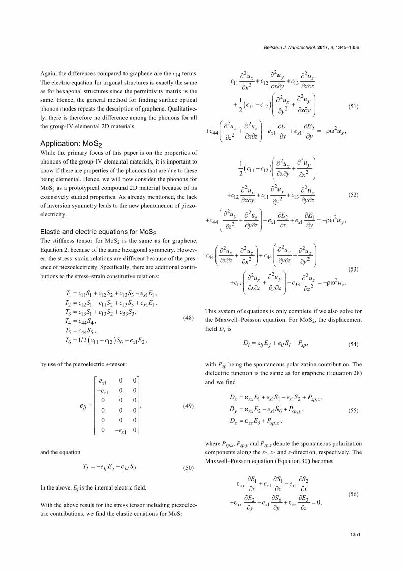
(48)
by use of the piezoelectric e-tensor:
(49)
and the equation
(50)
In the above, Ej is the internal electric field.
With the above result for the stress tensor including piezoelec-
tric contributions, we find the elastic equations for MoS2
(51)
(52)
(53)
This system of equations is only complete if we also solve for
the Maxwell–Poisson equation. For MoS2, the displacement
field Di is
(54)
with Psp being the spontaneous polarization contribution. The
dielectric function is the same as for graphene (Equation 28)
and we find
(55)
where Psp,x, Psp,y and Psp,z denote the spontaneous polarization
components along the x-, x- and z-direction, respectively. The
Maxwell–Poisson equation (Equation 30) becomes
(56)

Beilstein J. Nanotechnol. 2017, 8, 1345–1356.
1352
because the spontaneous polarization Psp is constant in space. A
solution of the combined system Equation 51–Equation 53 and
Equation 56 with appropriate boundary conditions allows for
the determination of the electric field (or electric potential
) and the displacements ux, uy and uz.
Phonon modesIn the case of MoS2, the general solutions are more compli-
cated. One can still make the plane wave ansatz,
(57)
(58)
(59)
(60)
Now, inserting Equation 57–Equation 60 in Equation 51–Equa-
tion 53 and Equation 56 yields the 4 × 4 matrix expression in
the unknown functions fx, fy, fz and
(61)
where
(62)
For the case, ky = 0, we have C = D2 = E2 = 0 and uy decouples
from ux, uz and . The wave equation for the uy mode is the
same as for graphene. To determine the general solution for the
other displacement components, we once again solve the deter-
minantal equation for the 3 × 3 sub-matrix in the components fx,
fz and . The result is
(63)
where
(64)
and six roots (three pairs of opposite signs) exist. It also follows
that
(65)
Hence the general solution is, using a notation similar to the
case of graphene,
(66)
(67)
(68)
where βi are unknown coefficients.
The Maxwell–Poisson equation in vacuum ( ) has the
general solution
(69)

Beilstein J. Nanotechnol. 2017, 8, 1345–1356.
1353
where are unknown constants. An 8 × 8 matrix equation
in βi, is finally obtained by invoking the four mechani-
cal boundary conditions at z = h,−h
(70)
(71)
and the four electric boundary conditions at z = h,−h,
(72)
The mechanical boundary conditions are the same as for
graphene,
(73)
but the electric boundary conditions are (written out)
(74)
where ε0 is the vacuum permittivity. Solving the determinantal
equation for the 8 × 8 matrix equation as a function of kx speci-
fies a discrete set of (band) eigenfrequencies ωi(kx) and the cor-
responding eigenmodes fx, fz and , where i denotes the band
index.
Confined phonon modesAn important result concerning confined optical phonons can be
obtained without solving the determinantal equations. From the
elastic equations (Equation 51 and Equation 53) and the elec-
tric equation (Equation 56) we have, assuming ky = 0,
(75)
(76)
(77)
Inspection of the above set of equations reveals that confined
phonon solutions can be sought in the form [type I]
(78)
or in the form [type II]
(79)
apart from a multiplying factor exp(ikxx − iωt). The above
choice reflects an expectation that four roots are real (two pairs
of opposite-signed roots) and two imaginary (one pair of oppo-
site-signed roots).
From Equation 75–Equation 77 follows
(80)
(81)
(82)
where i = 1,2,3. Note that a maximum of two of the latter rela-
tions can be independent since the values of δi are found by
setting the system determinant to zero.
A general confined optical phonon mode can now be written as
a Fourier series expansion [type I]

Beilstein J. Nanotechnol. 2017, 8, 1345–1356.
1354
(83)
(84)
(85)
since this construction implies Ex(z = ±h) = 0 and
using continuity in the transverse electric field at the interfaces.
Equation 75–Equation 77 must still apply, however, in particu-
lar combining Equation 81–Equation 82 demands
(86)
For each term m, this latter condition, in general, would lead to
a different ωm. However, a normal mode is characterized by a
unique frequency ω. Hence, for confined optical phonon modes,
only one term in m is allowed in the general Fourier series
expansions above. Further, imposing continuity in the normal
electric displacement component at z = ±h by use of the third
equation in Equation 55 gives
(87)
and unless accidentally εzz(ωm) = 0 (treated separately
in the next paragraph). For εzz(ωm) ≠ 0, it follows from Equa-
tion 80 that Ax,m = 0 and Equation 81 yields Az,m = 0. The
conclusion is that confined optical phonons in the general case
cannot exist in MoS2! Note that for graphene, since it is a non-
piezoelectric material, confined optical phonon modes do exist.
The difference between the two materials lies in Equation 77,
specifically in the term containing the piezoelectric coefficient.
If εzz = 0, continuity of the normal electric displacement compo-
nent requires, as before, and we return to the situa-
tion treated in the previous subsection about confined optical
phonons. We need to consider two possible cases: (a) εxx(ω) = 0
when εzz(ω) = 0 and (b) εxx(ω) ≠ 0 when εzz(ω) = 0. In case (a),
we immediately obtain from continuity in the
normal electric displacement. Further, Equation 77 yields ux = 0
everywhere as a function of z. Equation 83–Equation 85 must
hold from continuity in the transverse electric field. Finally,
Equation 75 gives
(88)
and Equation 76 requires [type I]
(89)
and the condition
(90)
which is not fulfilled, unless accidental degeneracy applies, si-
multaneous with εxx(ω) = εzz(ω) = 0. In case (b), Equation 86
can be used and, unless accidental degeneracy applies, the ob-
tained ωm values do not fulfill εzz(ω) = 0. In conclusion,
confined optical phonon modes do not exist in the case εzz = 0.
Computed dispersion relationsIn order to illustrate the validity of the phonon dispersion rela-
tions obtained from our model, we compare them to DFT calcu-
lations. The continuum theory will require as input elasticity
constants, piezoelectric coefficients, and dielectric functions.
DFTWe first give the standard phonon dispersion relation as ob-
tained from DFT calculations (Figure 1). They are obtained
from first principles calculations using the Vienna ab initio
simulation package (VASP) [17] with a kinetic energy cut-off
of 500 eV in the expansion of the electronic wave functions.
Four C and six Mo and S valence electrons are considered. The
generalized gradient approximation of the exchange–correla-
tion potential in the Perdew–Burke–Ernzerhof flavor is em-
ployed [18]. Brillouin-zone integrations are performed using the
tetrahedron method with Blöchl corrections [19]. We construct
cells consisting of the monolayer and an approximately 15 Å
thick vacuum region along the c direction. Structure optimiza-
tions are performed on Γ-centered 24 × 24 × 1 k-meshes. A
direct method based on 4 × 4 × 1 supercells is used for obtain-

Beilstein J. Nanotechnol. 2017, 8, 1345–1356.
1355
Figure 2: Dispersion relations for the coupled ux–uz acoustic phononmodes of single-layer graphene. The right plot is a zoomed version ofthe left plot. Note the nonlinear dispersion of one acoustic mode awayfrom the Γ point. There is also one acoustic mode showing lineardispersion.
ing the phonon dispersions within the harmonic approximation
[20]. Forces are evaluated on 3 × 3 × 1 k-meshes, including
long-range dipole contributions to the dynamical matrix
following the method of [21]. Born effective charges and
dielectric tensors are obtained within perturbation theory [22]
and elastic constants by the homogeneous deformation method
[23]. The elastic stiffness tensor and frequency-dependent
dielectric tensor (independent particle approximation [24]) are
calculated on Γ-centered 36 × 36 × 1 k-meshes.
Figure 1: Dispersion relations for the phonon modes of single-layergraphene (left) and MoS2 (right), from DFT calculations.
Continuum model: grapheneThe following parameters are found using DFT calculations
as explained above: c11d = 345 Pa·m, c12d = 73 Pa·m,
c13d = 0.00387 Pa·m, c33d = 0.531 Pa·m, c44d = 0.0535 Pa·m,
c66d = 136 Pa·m, d = 3.4·10−8 m, and ρ2D = 7.61·10−7 kg/m2.
For the permittivity data we used the DC values εxx = 4.4ε0 and
εzz = 1.3ε0.
In Figure 2, we show the frequency vs wavenumber (ω–kx)
dispersion in the vicinity of the Γ point (ky = 0). Evidently, one
mode shows a parabolic dispersion and one mode is linear.
There are two higher-order modes originating from the bound-
ary conditions along the z coordinate. The dispersion curves as-
sociated with the uy vibrations decoupled from the ux − uz vibra-
tions are not shown in the plots. We emphasize that for
graphene optical and acoustic phonon modes decouple and are
computed separately as described above. In Figure 3, the disper-
sion curves for optical phonon modes near the Γ point are
shown.
Figure 3: Dispersion relation for the optical phonon modes of single-layer graphene.
Continuum model: MoS2For single-layer MoS2, we use the following parameters:
c11d = 140 Pa·m, c12d = 33 Pa·m, c13d=-0.013 Pa·m,
c33d = 0.078 Pa·m, c44d = −1.07 Pa·m, c66d = 53.7 Pa·m,
d = 6.2·10−10 m, ρ2D = 3.1 ·10−6 kg/m2, ex1 = 0.5 C/m2. These
elasticity parameters were again computed using VASP. The
frequency-dependent permittivity values are taken from [25]
and the piezoelectric constant ex1 is from Ref. [26]. In the case
of MoS2, all optical and acoustic phonon modes are computed
by solving the combined set of elastic and electric equations and
associated slab boundary conditions as described above. We
note in passing that both confined and surface acousto-optical
phonon modes are found using the present formalism. In
Figure 4, we show the frequency vs wavenumber (ω–kx) disper-
sion in the vicinity of the Γ point (ky = 0).
ConclusionA three-dimensional, first-principles, continuum elasticity
theory was developed for two-dimensional materials. Piezoelec-
tric materials required the simultaneous consideration of the
electrostatics equations. Application to graphene, silicene and
MoS2 revealed a number of interesting results. The out-of-plane
vibrations were coupled to the in-plane motion for graphene
(and for silicene as well), contrary to previous results using infi-
nitely thin sheets. Acoustic modes with linear and quadratic
dispersions were obtained, in agreement with experimental
results and other models. We predict the existence of confined
optical modes in all of the elemental group-IV materials and the
nonexistence of confined optical modes in MoS2. Our model

Beilstein J. Nanotechnol. 2017, 8, 1345–1356.
1356
Figure 4: Dispersion relations for the coupled ux–uz– phonon modesof single-layer MoS2. The right plot is a zoomed version of the left plot.Note again the parabolic dispersion of one predominantly acousticmode away from the Γ point besides a linear dispersion predominantacoustic mode. We also obtain a second nonlinear mode starting at(k,ω) = (0,0), which stems from the rather complicated frequency-de-pendent permittivity of MoS2.
will be applied to other 2D materials as well as to multilayers in
future work. Additionally, the results of this model can be
combined with the solution to the electron problem to compute
electron–phonon scattering rates. The latter would be useful for
understanding a number of physical properties as well as for ap-
plications.
AcknowledgementsMW acknowledges financial support from the Danish Council
of Independent Research (Natural Sciences) grant no.: DFF -
4181-00182. The research reported in this publication was sup-
ported by funding from King Abdullah University of Science
and Technology (KAUST).
References1. Cahangirov, S.; Topsakal, M.; Aktürk, E.; Şahin, H.; Ciraci, S.
Phys. Rev. Lett. 2009, 102, 236804.doi:10.1103/PhysRevLett.102.236804
2. Roome, N. J. Electronic and Phonon Properties of 2D LayeredMaterials. Ph.D. Thesis, University of Surrey, United Kingdom, 2015.
3. Kamal, C.; Chakrabarti, A.; Ezawa, M. New J. Phys. 2015, 17, 083014.doi:10.1088/1367-2630/17/8/083014
4. Mannix, A. J.; Zhou, X.-F.; Kiraly, B.; Wood, J. D.; Alducin, D.;Myers, B. D.; Liu, X.; Fisher, B. L.; Santiago, U.; Guest, J. R.;Yacaman, M. J.; Ponce, A.; Oganov, A. R.; Hersam, M. C.;Guisinger, N. P. Science 2015, 350, 1513–1516.doi:10.1126/science.aad1080
5. Peng, B.; Zhang, H.; Shao, H.; Xu, Y.; Zhang, R.; Zhu, H.J. Mater. Chem. C 2016, 4, 3592–3598. doi:10.1039/C6TC00115G
6. Singh, D.; Gupta, S. K.; Lukačevic, I.; Sonvane, Y. RSC Adv. 2016, 6,8006–8014. doi:10.1039/C5RA25773E
7. Guzmán-Verri, G. G.; Lew Yan Voon, L. C. Phys. Rev. B 2007, 76,075131. doi:10.1103/PhysRevB.76.075131
8. Takeda, K.; Shiraishi, K. Phys. Rev. B 1994, 50, 14916–14922.doi:10.1103/PhysRevB.50.14916
9. Fuchs, R.; Kliewer, K. L. Phys. Rev. 1965, 140, A2076–A2088.doi:10.1103/PhysRev.140.A2076
10. Suzuura, H.; Ando, T. Phys. Rev. B 2002, 65, 235412.doi:10.1103/PhysRevB.65.235412
11. Goupalov, S. V. Phys. Rev. B 2005, 71, 085420.doi:10.1103/PhysRevB.71.085420
12. Qian, J.; Allen, M. J.; Yang, Y.; Dutta, M.; Stroscio, M. A.Superlattices Microstruct. 2009, 46, 881–888.doi:10.1016/j.spmi.2009.09.001
13. Droth, M.; Burkard, G. Phys. Rev. B 2011, 84, 155404.doi:10.1103/PhysRevB.84.155404
14. Landau, L. D.; Lifshitz, E. M. Theory of Elasticity, 2nd ed.; Course oftheoretical physics, Vol. 7; Pergamon Press: Oxford, United Kingdom,1970.
15. Xie, H.; Hu, M.; Bao, H. Appl. Phys. Lett. 2014, 104, 131906.doi:10.1063/1.4870586
16. Licari, J. J.; Evrard, R. Phys. Rev. B 1977, 15, 2254–2264.doi:10.1103/PhysRevB.15.2254
17. Kresse, G.; Joubert, D. Phys. Rev. B 1999, 59, 1758–1775.doi:10.1103/PhysRevB.59.1758
18. Perdew, J. P.; Burke, K.; Ernzerhof, M. Phys. Rev. Lett. 1996, 77,3865–3868. doi:10.1103/PhysRevLett.77.3865
19. Blöchl, P. E.; Jepsen, O.; Andersen, O. K. Phys. Rev. B 1994, 49,16223–16233. doi:10.1103/PhysRevB.49.16223
20. Alfè, D. Comput. Phys. Commun. 2009, 180, 2622–2633.doi:10.1016/j.cpc.2009.03.010
21. Cochran, W.; Cowley, R. A. J. Phys. Chem. Solids 1962, 23, 447–450.doi:10.1016/0022-3697(62)90084-7
22. Baroni, S.; Giannozzi, P.; Testa, A. Phys. Rev. Lett. 1987, 58,1861–1864. doi:10.1103/PhysRevLett.58.1861
23. Le Page, Y.; Saxe, P. Phys. Rev. B 2002, 65, 104104.doi:10.1103/PhysRevB.65.104104
24. Gajdoš, M.; Hummer, K.; Kresse, G.; Furthmüller, J.; Bechstedt, F.Phys. Rev. B 2006, 73, 045112. doi:10.1103/PhysRevB.73.045112
25. Mukherjee, B.; Tseng, F.; Gunlycke, D.; Amara, K. K.; Eda, G.;Simsek, E. Opt. Mater. Express 2015, 5, 447–455.doi:10.1364/OME.5.000447
26. Zhu, H.; Wang, Y.; Xiao, J.; Liu, M.; Xiong, S.; Wong, Z. J.; Ye, Z.;Ye, Y.; Yin, X.; Zhang, X. Nat. Nanotechnol. 2015, 10, 151–155.doi:10.1038/nnano.2014.309
License and TermsThis is an Open Access article under the terms of the
Creative Commons Attribution License
(http://creativecommons.org/licenses/by/4.0), which
permits unrestricted use, distribution, and reproduction in
any medium, provided the original work is properly cited.
The license is subject to the Beilstein Journal of
Nanotechnology terms and conditions:
(http://www.beilstein-journals.org/bjnano)
The definitive version of this article is the electronic one
which can be found at:
doi:10.3762/bjnano.8.136


![[XLS] · Web viewF.NO-208,CLASSIC ARCADE,CZECH COLONY,STREET NO.-1,SANATH NAGAR,NEAR FCI GODOWN SANATH NAGAR VASUDHA DANNANA ****aisolarsystems@gmail.com APPALA NAIDU DANNANA LAKSHMI](https://img.pdfslide.us/doc/110x75/5aa58a8a7f8b9a517d8d5fd9/xls-viewfno-208classic-arcadeczech-colonystreet-no-1sanath-nagarnear-fci.jpg)