Embed Size (px)
Citation preview

CHR3894-QEG
37-40GHz Integrated Down Converter GaAs Monolithic Microwave IC in SMD leadless package
Description
The CHR3894-QEG is a multifunction monolithic receiver, which integrates a balanced cold FET mixer, a LO chain with buffers associated to a time two multiplier, and a RF low noise amplifier including gain control. It is designed for a wide range of applications, from military to commercial communication systems. The circuit is manufactured with a pHEMT process, 0.15µm gate length, via holes through the substrate, air bridges and electron beam gate lithography. It is supplied in RoHS compliant SMD package. Main Features
Broadband performances: 37-40GHz 13dB Conversion gain 15dBc Image Rejection 2dBm IIP3 without attenuation (GC=-2V) 8dB Gain Control range 4dB Noise Figure for IF>0.1GHz 0dBm LO input Power DC bias: Vd=4V @ Id=250mA 24L-QFN4x5 MSL1 Main Electrical Characteristics Tamb.= +25°C Symbol Parameter Min Typ Max Unit
FRF RF frequency range 37 40 GHz FLO LO frequency range 17.5 21.0 dB FIF IF frequency range DC 3.5 dB G Conversion gain without attenuation 10 13 dBm
UMSR3894
YYWW
UMSR3894
YYWW
UMSR3894
YYWW
0
2
4
6
8
10
12
14
16
18
20
35 36 37 38 39 40 41
Con
vers
ion
gain
(dB
)
RF Frequency (GHz)
Conversion gain (USB mode) @ IF 2GHz
-2V -0.4V -0.2V 0V +0.6V
Ref. : DSCHR3894-QEG5336 - 02 Dec 15 1/14 Specifications subject to change without notice United Monolithic Semiconductors S.A.S.
Bât. Charmille - Parc SILIC - 10, Avenue du Québec - 91140 VILLEBON-SUR-YVETTE - France Tel.: +33 (0) 1 69 86 32 00 - Fax: +33 (0) 1 69 86 34 34
CHR3894-QEG 37-40GHz Integrated Down Converter
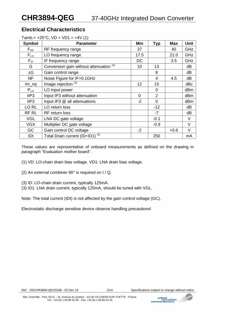
Electrical Characteristics Tamb.= +25°C, VD = VD1 = +4V (1) Symbol Parameter Min Typ Max Unit
FRF RF frequency range 37 40 GHz FLO LO frequency range 17.5 21.0 GHz FIF IF frequency range DC 3.5 GHz G Conversion gain without attenuation (2) 10 13 dB ∆G Gain control range 8 dB NF Noise Figure for IF>0.1GHz 4 4.5 dB
Im_rej Image rejection (2) 12 15 dBc PLO LO Input power 0 dBm IIP3 Input IP3 without attenuation 0 2 dBm IIP3 Input IP3 @ all attenuations -2 0 dBm
LO RL LO return loss -12 dB RF RL RF return loss -7 dB VGL LNA DC gate voltage -0.1 V VGX Multiplier DC gate voltage -0.9 V GC Gain control DC voltage -2 +0.6 V IDt Total Drain current (ID+ID1) (3) 250 mA
These values are representative of onboard measurements as defined on the drawing in paragraph "Evaluation mother board". (1) VD: LO-chain drain bias voltage. VD1: LNA drain bias voltage. (2) An external combiner 90° is required on I / Q. (3) ID: LO-chain drain current, typically 125mA. (3) ID1: LNA drain current, typically 125mA, should be tuned with VGL. Note: The total current (IDt) is not affected by the gain control voltage (GC). Electrostatic discharge sensitive device observe handling precautions!
Ref. : DSCHR3894-QEG5336 - 02 Dec 15 2/14 Specifications subject to change without notice
Bât. Charmille - Parc SILIC - 10, Avenue du Québec - 91140 VILLEBON-SUR-YVETTE - France Tel.: +33 (0) 1 69 86 32 00 - Fax: +33 (0) 1 69 86 34 34
37-40GHz Integrated Down Converter CHR3894-QEG
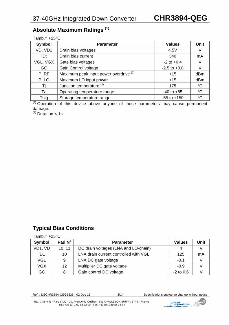
Absolute Maximum Ratings (1) Tamb.= +25°C
Symbol Parameter Values Unit VD, VD1 Drain bias voltages 4.5V V
IDt Drain bias current 340 mA VGL, VGX Gate bias voltages -2 to +0.4 V
GC Gain Control voltage -2.5 to +0.8 V P_RF Maximum peak input power overdrive (2) +15 dBm P_LO Maximum LO input power +15 dBm
Tj Junction temperature (2) 175 °C Ta Operating temperature range -40 to +85 °C
Tstg Storage temperature range -55 to +150 °C (1) Operation of this device above anyone of these parameters may cause permanent damage. (2) Duration < 1s. Typical Bias Conditions Tamb.= +25°C Symbol Pad No Parameter Values Unit VD1, VD 10, 11 DC drain voltages (LNA and LO-chain) 4 V
ID1 10 LNA drain current controlled with VGL 125 mA VGL 9 LNA DC gate voltage -0.1 V VGX 12 Multiplier DC gate voltage -0.9 V GC 8 Gain control DC voltage -2 to 0.6 V
Ref. : DSCHR3894-QEG5336 - 02 Dec 15 3/14 Specifications subject to change without notice
Bât. Charmille - Parc SILIC - 10, Avenue du Québec - 91140 VILLEBON-SUR-YVETTE - France Tel.: +33 (0) 1 69 86 32 00 - Fax: +33 (0) 1 69 86 34 34
CHR3894-QEG 37-40GHz Integrated Down Converter
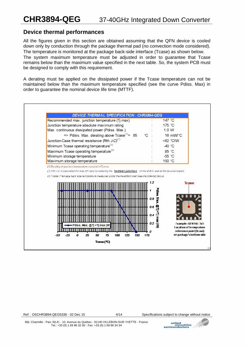
Device thermal performances All the figures given in this section are obtained assuming that the QFN device is cooled down only by conduction through the package thermal pad (no convection mode considered). The temperature is monitored at the package back-side interface (Tcase) as shown below. The system maximum temperature must be adjusted in order to guarantee that Tcase remains below than the maximum value specified in the next table. So, the system PCB must be designed to comply with this requirement. A derating must be applied on the dissipated power if the Tcase temperature can not be maintained below than the maximum temperature specified (see the curve Pdiss. Max) in order to guarantee the nominal device life time (MTTF).
Ref. : DSCHR3894-QEG5336 - 02 Dec 15 4/14 Specifications subject to change without notice
Bât. Charmille - Parc SILIC - 10, Avenue du Québec - 91140 VILLEBON-SUR-YVETTE - France Tel.: +33 (0) 1 69 86 32 00 - Fax: +33 (0) 1 69 86 34 34

37-40GHz Integrated Down Converter CHR3894-QEG
Typical Board Measurements Tamb.= +25°C, VD = VD1 =+4V, VGL = -0.1V, VGX = -0.9V, P_LO = 0dBm (IDt = 250mA) These values are representative of onboard measurements as defined on the drawing in paragraph "Evaluation mother board". Data given in the package access planes.
Conversion Gain versus RF & IF frequency (USB & LSB modes)
without attenuation: GC= -2V
Conversion Gain versus RF frequency and gain control voltage (IF 2GHz, USB mode)
0
2
4
6
8
10
12
14
16
18
20
35 36 37 38 39 40 41
Con
vers
ion
Gai
n (d
B)
RF Frequency (GHz)
LSB- 2GHz USB- 2GHz
LSB- 3.5GHz USB- 3.5GHz
0
2
4
6
8
10
12
14
16
18
20
35 36 37 38 39 40 41
Con
vers
ion
gain
(dB
)
RF Frequency (GHz)
-2V -0.4V -0.2V 0V +0.6V
Ref. : DSCHR3894-QEG5336 - 02 Dec 15 5/14 Specifications subject to change without notice
Bât. Charmille - Parc SILIC - 10, Avenue du Québec - 91140 VILLEBON-SUR-YVETTE - France Tel.: +33 (0) 1 69 86 32 00 - Fax: +33 (0) 1 69 86 34 34

CHR3894-QEG 37-40GHz Integrated Down Converter
Typical Board Measurements Tamb.= +25°C, VD = VD1 = +4V, VGL = -0.1V, VGX = -0.9V, P_LO = 0dBm (IDt = 250mA)
Noise figure versus RF frequency at IF 2GHz (USB & LSB modes)
without attenuation: GC= -2V
Noise figure versus gain control range (IF 2GHz, USB mode)
0
1
2
3
4
5
6
7
8
9
10
35 36 37 38 39 40 41 42
Noi
se F
igur
e (d
B)
RF Frequency (GHz)
USB LSB
0
1
2
3
4
5
6
7
8
9
10
35 36 37 38 39 40 41 42
Noi
se F
igur
e (d
B)
RF Frequency (GHz)
-2V -0.2V 0V +0.6V
Ref. : DSCHR3894-QEG5336 - 02 Dec 15 6/14 Specifications subject to change without notice
Bât. Charmille - Parc SILIC - 10, Avenue du Québec - 91140 VILLEBON-SUR-YVETTE - France Tel.: +33 (0) 1 69 86 32 00 - Fax: +33 (0) 1 69 86 34 34

37-40GHz Integrated Down Converter CHR3894-QEG
Typical Board Measurements Tamb.= +25°C, VD = VD1 = +4V, VGL = -0.1V, VGX = -0.9V, P_LO = 0dBm (IDt = 250mA)
Image rejection versus RF frequency at IF 2GHz (USB & LSB modes)
without attenuation: GC= -2V
Return Losses (LO & RF) versus frequency and gain control voltage
0
4
8
12
16
20
24
28
32
36
40
44
35 36 37 38 39 40 41
Imag
e re
ject
ion
(dB
c)
RF Frequency (GHz)
USB LSB
-20
-18
-16
-14
-12
-10
-8
-6
-4
-2
0
0 5 10 15 20 25 30 35 40 45
Frequency (GHz)
LO &
RF
Ret
urn
loss
es (d
B)
RF @ GC=-2V RF @ GC=0.6V LO
Ref. : DSCHR3894-QEG5336 - 02 Dec 15 7/14 Specifications subject to change without notice
Bât. Charmille - Parc SILIC - 10, Avenue du Québec - 91140 VILLEBON-SUR-YVETTE - France Tel.: +33 (0) 1 69 86 32 00 - Fax: +33 (0) 1 69 86 34 34

CHR3894-QEG 37-40GHz Integrated Down Converter
Typical Board Measurements Tamb.= +25°C, VD = VD1 = +4V, VGL = -0.1V, VGX = -0.9V, P_LO = 0dBm (IDt = 250mA) Input IP3 vs RF frequency at IF 3.5GHz
without attenuation: GC= -2V IMD3 vs RF frequency at IF 3.5GHz
without attenuation: GC= -2V
Input IP3 vs gain control at 38.5GHz Input IP3 vs temperature at 38.5GHz without attenuation: GC= -2V
-6
-4
-2
0
2
4
6
8
10
-24 -22 -20 -18 -16 -14 -12 -10Input Power DCL (dBm)
IIP3
(dB
m)
37.5GHz 38.5GHz
39.5GHz 40.5GHz05
10152025303540455055606570
-24 -22 -20 -18 -16 -14 -12 -10Input Power DCL (dBm)
IMD
3 (d
Bc)
37.5GHz 38.5GHz
39.5GHz 40.5GHz
-6
-4
-2
0
2
4
6
8
10
-24 -22 -20 -18 -16 -14 -12 -10Input Power DCL (dBm)
IIP3
(dB
m)
-2V -0.5V -0.4V 0V +0.6V
-6
-4
-2
0
2
4
6
8
10
-24 -22 -20 -18 -16 -14 -12 -10Input Power DCL (dBm)
IIP3
(dB
m)
85°C 25°C -40°C
Ref. : DSCHR3894-QEG5336 - 02 Dec 15 8/14 Specifications subject to change without notice
Bât. Charmille - Parc SILIC - 10, Avenue du Québec - 91140 VILLEBON-SUR-YVETTE - France Tel.: +33 (0) 1 69 86 32 00 - Fax: +33 (0) 1 69 86 34 34

37-40GHz Integrated Down Converter CHR3894-QEG
Typical Board Measurements Tamb = +25°C, Tcold = -40°C, Thot = +85°C VD = VD1 = +4V, VGL = -0.1V, VGX = -0.9V, P_LO = 0dBm
Conversion Gain versus temperature at IF 2GHz (USB mode)
without attenuation: GC= -2V
Noise figure versus temperature at IF 2GHz (USB mode) without attenuation: GC= -2V
4
6
8
10
12
14
16
18
20
22
24
35 36 37 38 39 40 41
RF Frequency (GHz)
Con
vers
ion
gain
(dB
)
85°C 25°C -40°C
0
1
2
3
4
5
6
7
8
9
10
35 36 37 38 39 40 41 42
Noi
se F
igur
e (d
B)
RF Frequency (GHz)
85°C 25°C -40°C
Ref. : DSCHR3894-QEG5336 - 02 Dec 15 9/14 Specifications subject to change without notice
Bât. Charmille - Parc SILIC - 10, Avenue du Québec - 91140 VILLEBON-SUR-YVETTE - France Tel.: +33 (0) 1 69 86 32 00 - Fax: +33 (0) 1 69 86 34 34
CHR3894-QEG 37-40GHz Integrated Down Converter
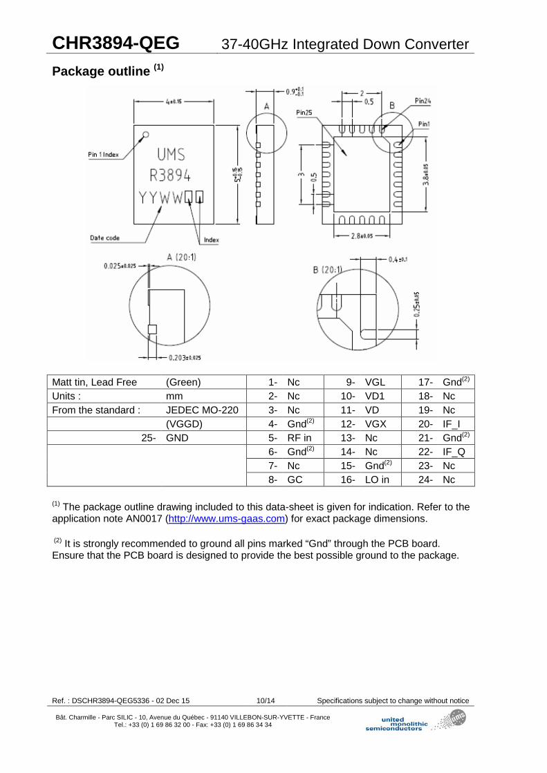
Package outline (1)
Matt tin, Lead Free (Green) 1- Nc 9- VGL 17- Gnd(2) Units : mm 2- Nc 10- VD1 18- Nc From the standard : JEDEC MO-220 3- Nc 11- VD 19- Nc (VGGD) 4- Gnd(2) 12- VGX 20- IF_I
25- GND 5- RF in 13- Nc 21- Gnd(2) 6- Gnd(2) 14- Nc 22- IF_Q 7- Nc 15- Gnd(2) 23- Nc 8- GC 16- LO in 24- Nc (1) The package outline drawing included to this data-sheet is given for indication. Refer to the application note AN0017 (http://www.ums-gaas.com) for exact package dimensions. (2) It is strongly recommended to ground all pins marked “Gnd” through the PCB board. Ensure that the PCB board is designed to provide the best possible ground to the package.
Ref. : DSCHR3894-QEG5336 - 02 Dec 15 10/14 Specifications subject to change without notice
Bât. Charmille - Parc SILIC - 10, Avenue du Québec - 91140 VILLEBON-SUR-YVETTE - France Tel.: +33 (0) 1 69 86 32 00 - Fax: +33 (0) 1 69 86 34 34

37-40GHz Integrated Down Converter CHR3894-QEG
Evaluation mother board Compatible with the proposed footprint.
Based on typically Ro4003 / 8mils or equivalent. Using a micro-strip to coplanar transition to access the package. Recommended for the implementation of this product on a module board. Decoupling capacitors of 10nF ±10% are recommended for all DC accesses. See application note AN0017 for details. Hybrid coupler 90° for 2-4GHz.
IF_IIF_Q
RF IN
LO IN
IF_IIF_Q
RF IN
LO IN
Ref. : DSCHR3894-QEG5336 - 02 Dec 15 11/14 Specifications subject to change without notice
Bât. Charmille - Parc SILIC - 10, Avenue du Québec - 91140 VILLEBON-SUR-YVETTE - France Tel.: +33 (0) 1 69 86 32 00 - Fax: +33 (0) 1 69 86 34 34

CHR3894-QEG 37-40GHz Integrated Down Converter
Notes Due to ESD protection circuits on RF input and output, an external capacitance might be requested to isolate the product from external voltage that could be present on the RF accesses.
ESD protections are also implemented on gate and control accesses. The DC connections do not include any decoupling capacitor in package, therefore it is mandatory to provide a good external DC decoupling (10nF) on the PC board, as close as possible to the package.
Ref. : DSCHR3894-QEG5336 - 02 Dec 15 12/14 Specifications subject to change without notice
Bât. Charmille - Parc SILIC - 10, Avenue du Québec - 91140 VILLEBON-SUR-YVETTE - France Tel.: +33 (0) 1 69 86 32 00 - Fax: +33 (0) 1 69 86 34 34

37-40GHz Integrated Down Converter CHR3894-QEG
DC Schematic
LNA: 4V, 125mA
LO chain: 4V, 125mA
27Ω
VGL# -0.1V
2kΩ
53mA34Ω
43mA
VD1
10mA
150Ω576Ω
1.9kΩ 15Ω
1kΩ
5kΩ
RF
x4
15mA
90Ω444Ω
1.6kΩ 15Ω
2kΩ
1kΩ
x4GC
1kΩ
27Ω
VGL# -0.1V
2kΩ2kΩ
53mA34Ω
43mA
VD1
10mA
150Ω150Ω576Ω
1.9kΩ 15Ω
1kΩ
5kΩ
RF
x4x4
15mA
90Ω90Ω444Ω
1.6kΩ 15Ω
2kΩ
1kΩ
x4x4GC
1kΩ
2kΩ
200Ω
185Ω
30Ω
16Ω
VD
45mA25mA @Pin=0dBm 50mA
LO
VGX=-0.9V
26Ω
18Ω
800Ω
70Ω
Mixer Gate
700Ω515Ω
515Ω
x2
Ref. : DSCHR3894-QEG5336 - 02 Dec 15 13/14 Specifications subject to change without notice
Bât. Charmille - Parc SILIC - 10, Avenue du Québec - 91140 VILLEBON-SUR-YVETTE - France Tel.: +33 (0) 1 69 86 32 00 - Fax: +33 (0) 1 69 86 34 34
CHR3894-QEG 37-40GHz Integrated Down Converter
Recommended package footprint Refer to the application note AN0017 available at http://www.ums-gaas.com for package foot print recommendations. SMD mounting procedure For the mounting process standard techniques involving solder paste and a suitable reflow process can be used. For further details, see application note AN0017. Recommended environmental management UMS products are compliant with the regulation in particular with the directives RoHS N°2011/65 and REACh N°1907/2006. More environmental data are available in the application note AN0019 also available at http://www.ums-gaas.com. Recommended ESD management Refer to the application note AN0020 available at http://www.ums-gaas.com for ESD sensitivity and handling recommendations for the UMS package products. Ordering Information QFN 4x5 package: CHR3894-QEG/XY Stick: XY = 20 Tape & reel: XY = 21 Information furnished is believed to be accurate and reliable. However United Monolithic Semiconductors S.A.S. assumes no responsibility for the consequences of use of such information nor for any infringement of patents or other rights of third parties which may result from its use. No license is granted by implication or otherwise under any patent or patent rights of United Monolithic Semiconductors S.A.S.. Specifications mentioned in this publication are subject to change without notice. This publication supersedes and replaces all information previously supplied. United Monolithic Semiconductors S.A.S. products are not authorised for use as critical components in life support devices or systems without express written approval from United Monolithic Semiconductors S.A.S.
Ref. : DSCHR3894-QEG5336 - 02 Dec 15 14/14 Specifications subject to change without notice
Bât. Charmille - Parc SILIC - 10, Avenue du Québec - 91140 VILLEBON-SUR-YVETTE - France Tel.: +33 (0) 1 69 86 32 00 - Fax: +33 (0) 1 69 86 34 34