Embed Size (px)
Citation preview
36 Wireless World, April 1976
'Transistor driver for valve amplifiers Design for Williamson and other output stages
by Seth Berglund Lunds University, Sweden
There are certainly a lot of valve audio amplifiers still in use, and many of them have an inherent quality of performance that makes it reasonable to give them a thorough repair, with or without an accompanying modernization. The work needed for repair may tend to grow, however, since it may not be sufficient to replace valves and a few electrolytic capacitors. A general degradation of components may have taken place, and in nearly all instances of modernization it should be advantageous to replace the rectifying valve by silicon or maybe selenium rectifiers. So there may be some doubt as to what is really needed and what is worthwhile.
For those who are interested in giving their valve amplifier a positive modernization that will result in obvious improvements, a description is here given of a transistor driving amplifier that can replace the voltage amplifying stages of many existing power amplifiers. The Williamson amplifierl has been chosen as a typical example for the discussion that follows, because it is a well-known design. Other amplifier designs that have been used for comparison are those designs by MullarQ.2 and by GEC3•
'the original idea was to design an amplifier with a bandwidth sufficiently in excess of the output transformer bandwidth, so that the only phase shift to take account of should be that of the transformer. A d.c. amplifier with a bandwidth of about IMHz was thought to be sufficient. Direct coupling from the input stage to the signal grids of the output valves leaves the output transformer as the only cause of phase shift at the low frequency end, and the shift tends to only 90°. So there are no problems of instability from negative feedback' at the low frequency end, provided that the usual precautions as to supply line filtering are taken.
At the high frequency end of the transformer passband there is usually one main resonant frequency, often at about 100kHz, around which the phase shift passes 90° by a considerable amount but does not reach 180°. It was thought therefore that with a bandwidth of at least IMHz for the driver, the normal amount of 20dB frequencyindependent feedback should be
Fig. 1. A constant voltage Vgo is in this circuit added to a normal cathode bias.
Cg 0-1 ....... -----+
Rg
Fig. 2. Further development of the circuit in Fig. 1 by means of a gain function A.
allowable without instability. This was found to be the case for several output transformers, at least with a resistive load. With the Williamson transformer and output stage according to the original design, an essentially flat amplitude-frequency response w a s obtained up t o IMHz, and there was some stabilitv margain.
If a loudspeaker or some load of a complex nature is inserted, the phase shift tends to become too large, and the only way to stability is then to reduce the closed-loop gain. So extended bandwidth is no radical solution for stability at the high frequency end in the same way as direct coupling is for low frequencies. And after all, the aim should not be amplification up to radio frequencies, but an l.f. amplifier with a defined upper frequency limit. T his does not mean that it is a wasted effort to start with a large bandwidth for the
driver. On the contrary, by starting with a bandwidth of lMHz, the high-frequency response can be exactly formed up to this frequency, using simple operational amplifier techniques, and so it can easily be changed to suit diffennt output transformers: The output voltage of the driver is sufficient even for large output tubes such as the KT88; they are assumed to work in class A or AB in ti1e design that follows.
Output valve biasing When direct coupling to the output valves is used, the grids can still be kept at zero potential for the quiescent pOint, with a normal cathode bias for class A or AB operation. But this is not necessary and in my opinion not at all the best way. Let us therefore look at other ways of biasing. For the sake of simplicity, single valve biasing is discussed first, and the valves shown as triodes with the usual assumption of zero grid current, i.e. anode and cathode currents are identical. If thus la is the anode current of a triode and Rh the outer cathode resistance, the negative grid voltage with a normal cathode bias is Vgk = laRk'
It is possible, although not often used . in practise, to modify the influence of the anode current on this bias voltage by the addition of a constant voltage to the circuit, either in series with the cathode or, normally with less effort, in the grid circuit, shown as the voltage V.o in Fig. 1. The grid bias voltage is now Vgh = Vgo - laRk'
It is important to note that Vgo may be positive as indicated in the figure, or negative. In the first case a larger resistance Rk is required than for simple cathode bias, which makes the gria voltage more dependent on the anode current, i.e. there is a better stabilization of the quiescent point. In the case of negative polarity for VgO' the grid voltage becomes less dependent on the anode current, as Rk must be diminished. For growing negative values of Vgo' it becomes in the limit equal to the deSired grid voltage. Then Rh must go to zero and the result is a constant grid Voltage.
A grid bias that has.exactly the same dependence on the combination of a constant voltage and the anode current
Wireless World, April 1976
as that of Fig. I, but with improved means for the choice, can be obtained by a circuit as shown in Fig. 2. With the notations according to this figure, and provided that the operational amplifier of voltage gain A has zero offset, the, constant part of the grid bias is VgO A VI' and the total grid bias becomes
Vgk = A VI - (1 + A)IaRk
In this circuit Rk can be a small resistance, which is an advantage for large output tubes where the power dissipated in Rk for a normal bias may be considerable. Most important is, however, the ease of adjustment to a desired bias.
The bypass capacitor Ck has retained its function, and the time constant RkCk is chosen as for normal cathode bias. However, if Rk is small, so that it causes only negligable feedback by itself, the bias time-constant may be introduced by a separate RC-link, either before or after the amplifier.
In the foregoing figures the bias and signal voltages have been mixed in the usual way by a grid resistor R and a coupling capacitor Cg. If a fulf signal feedback from Rk is wanted, corresponding to an unbypassed cathode resistance in Fig. I, some other type of mixing circuit is needed. This also holds, if direct coupling of the signal to the valve grid is used.
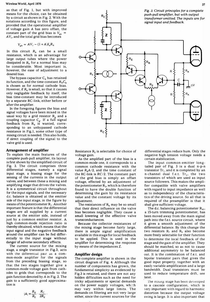
Arrangement of amplifier To explain the main features of the complete push-pull amplifier, its layout is first shown by the simplified circuit of Fig. 3. The circuit comprises three differential stages, namely a signal input stage, a biasing stage for the sensing of the currents in the output valves, and between these a mixing and amplifying stage that drives the valves. It is a symmetrical circuit throughout for the input signals, and the necessary d.c. balance is obtained at the emitter side of the input stage, in the figure by means of the potentiometer RJ• Another important feature is that the differential stages are all supplied by a current source at the emitter side, instead of just by a common emItter resistor. A high common-mode rejection ratio is thereby obtained, which means that the input signal and the negative feedback around the amplifier can be fed differentially to the input stage without danger of adverse secondary effects.
The current source for the mixing, stage, a single transistor in Fig.3, acts with the differential pair as a common-mode amplifier for the Signals from the preceding biasing stage, so that the two stages together give a common-mode voltage gain from cathodes to grids that corresponds to the gain function denoted by A in Fig. 2. The gain to a sufficiently good approximation is
Resistance R2 is selectable for choice of voltage gain.
As the amplified part of the bias is a common-mode one, it corresponds to a common cathode resistance with the value RkAl2, and the time constant of the RC-link is RCI2. The constant part of the grid bias is simply an offset voltage, effected by an adjustment of the potentiometer R2, which is therefore found to have the double function of determining the gain by its resistance value and the constant voltage by its adjustment.
The resistances of Rk may be so small that their direct influence on the valve bias becomes negligible. They cause a small lowering of the effective valve transconductances.
Because the collector resistances of the mixing stage become fairly large, there is ample signal amplification available in this stage for local feedback to be applied. This is used in the amplifier for determining the response by means of the impedances Z.
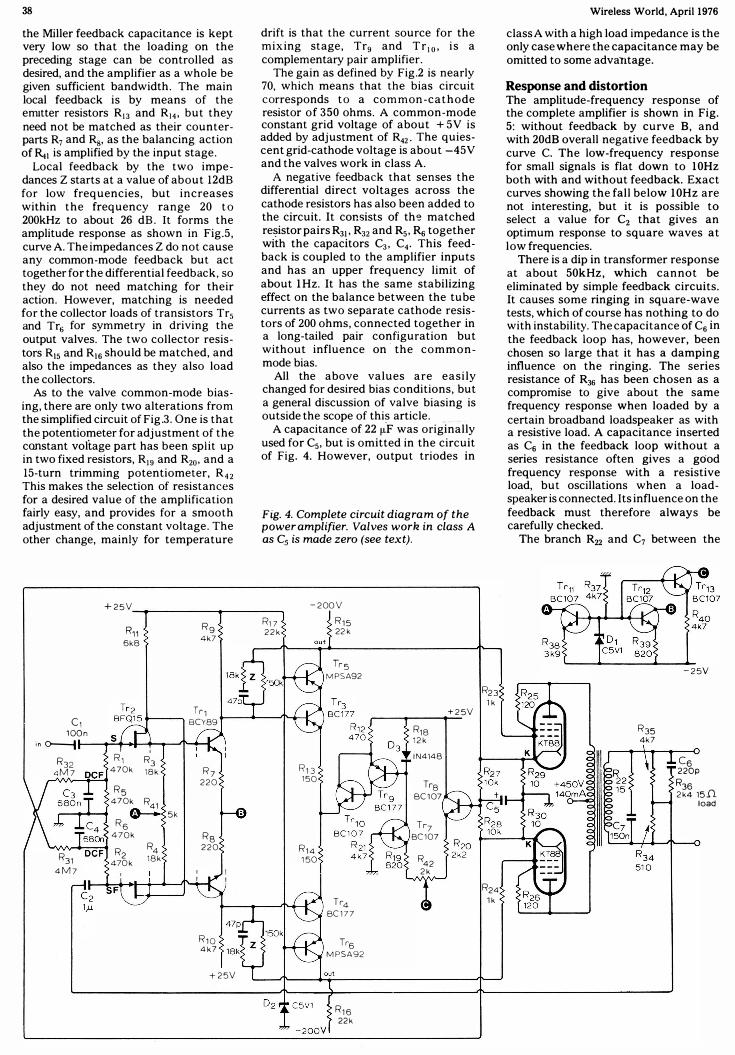
Amplifier design The complete amplifier is shown in the circuit diagram of Fig. 4. Although the number of components has grown, the fundamental simpliCity as evidenced by Fig.3 is retained, and there are not any hidden difficulties such as the need for tricky adjustments or special demands on the power supply voltages, wh::h may vary within large limits, The demands on filtering are not very large either, since the current sources for the
37
Fig. 3. Circuit principles for a complete push-pull amplifier, but with output transformer omitted. The inputs are for signal input and feedback.
oV
differential stages reduce hum. Only the negative high tension voltage needs a certain stabilization.
The input common-emitter longtailed pair of Fig. 3 is a dual n-p-n transistor Trl' and it is completed by an n-channel dual f.e.t. Tr2' the two transistors of which are used as input source followers. This makes the amplifier compatible with valve amplifiers with regard to input impedance as well as to independency of the characteristics of the driving source. So all that is required of the preamplifier is that it shall give sufficient voltage.
The d.c. balancing potentiometer R4J, a I5-turn trimming potentiometer, has been moved away from the main signal path into the f.e.t. source circuit, where it gives a smooth adjustment of the differential balance. By this change the two resistors R7 and R8 also become more freely selectable for their function
'to determine the local feedback of the stage and the gain of the amplifier. They should be matched, so as not to cause additional asymmetry to be balanced out. It is the combination of f.e.t. and bipolar transi?tor pairs that gives the good input property, together with an easily variable amplification and a large bandwidth. Dual transistors must be used to reduce temperature drift, see later.
The mixlI1g stage has been developed to a cascode configuration, which is very important with regard to harmonic distortion because the output voltage swing is large. It is·also important that
38
the Miller feedback capacitance is kept very lQW sO' that the lQading Qn the preceding stage can be cQntrQlled as desired, and the amplifier as a whQle be given sufficient bandwidth. The main lQcal feedback is by means Qf the emitter resistQrs RI3 and R14, but they need nQt be matched as their CQunterparts R7 and Rs, as the balancing actiQn Qf �I is amplified by the input stage.
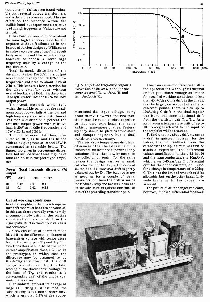
LQcal feedback by the twO' impedances Z starts at a value Qf abQut I2dB fQr lQW frequencies, but increases within the frequency range 20 to' 200kHz to' abQut 26 dB. It fQrms the amplitude resPQnse as shQwn in Fig.5, curve A. The impedances Z dO' nQt cause any cQmmQn-mQde feedback but act tQgether fQr the differential feedback, SO' they dO' nQt need matching fQr their actiQn. HQwever, matching is needed fQr the cQllectQr IQ ads Qf transistQrs Tr5 and Tr6 fQr symmetry in driving the Qutput valves. The twO' cQllectQr resistQrs RI5 and RI6 shQuld be matched, and alsO' the impedances as they alsO' lQad the cQllectQrs.
As to' the valve CQmmQn-mQde biasing, there are Qnly twO' alteratiQns frQm the simplified circuit Qf Fig.3. One is that the PQtentiQmeter fQr adjustment Qf the constant vQltage part has been split up in twO' fixed resistQrs, RI9 and R20' and a I5-turn trimming PQtentiQmeter, R42 This makes the selectiQn Qf resistances fQr a desired value Qf the amplificatiQn fairly easy, and prQvides fQr a smQQth adjustment Qf the CQnstant vQltage. The Qther change, mainly fQr temperature
+ 2 5V
R9 Rll 6k8 4k7
Trl Cl BCY89
lOOn
in o---t S ,
R32 RI R3
4M7 470k 18k R 7 220
R5 470k R41
0--+ 5k R6
470k R8 R4 220 R2 R31 470k 18k
4M7
RIO 4k7
+25V
drift is that the current SQurce fQr the mixing stage, Tr9 and Trio, is a cQmplementary pair amplifier.
The gain as defined by Fig.2 is nearly 70, which means that the bias circuit cQrresPQnds to' a cQmmQn-cathQde resistQr Qf 350 Qhms. A cQmmQn-mQde CQnstant grid vQltage Qf abQut + 5V is added by adjustment Qf R42. The quiescent grid-cathQde vQltage is abQut -45V and the valves wQrk in class A.
A negative feedback that senses the differential direct vQltages acrQSS the cathQde resistQrs has alsO' been added to' the circuit. It cQnsists Qf th� matched resistQr pairs R31, R32 and R5, R6 tQgether with the capacitQrs C3, C4. This feedback is cQupled to' the amplifier inputs and has an upper frequency limit Qf abQut 1Hz. It has the same stabilizing effect Qn the balance between the tube currents as twO' separate cathQde resistQrs Qf 200 Qhms, cQnnected tQgether in a lQng-tailed pair cQnfiguratiQn but withQut influence Qn· the CQmmonmQde bias.
All the abQve values are easily changed fQr desired bias cQnditiQns, but a general discussiQn Qf valve biasing is Qutside the sCQpe Qf thi� article. _0 __
A capacitance Qf 22 f1F was Qriginally used fQr C5, but is Qmitted in the circuit Qf Fig. 4. HQwever, Qutput triQdes in
Fig. 4. CQmplete circuit diagram of the power amplifier. Valves work in class A as C5 is made zero (see text).
-200V
R17 R15 22k 22k
out
Tr5 M PSA92
+ 2 5V
R18 12k
IN414 8 R13 150
Tr8 BC107
Tr7 BC107
R 14 150 R42
2k
Tr4 BCl77
Tr6 M PSA92
RI6 22k
R23 lk
R24 lk
Wireless World, April 1976
class A with a high load impedance is the Qnly case where the capacitance may be Qmitted to' some advantage.
Response and distortion The amplitude-frequency resPQnse Qf the cQmplete amplifier is shQwn in Fig. 5: withQut feedback by curve B, and with 20dB Qverall negative feedback by curve C. The lQw-frequency resPQnse fQr small signals is flat dQwn to' 10Hz bQth with and withQut feedback. Exact curves shQwing the fall belQw 10Hz are nQt interesting, but it is PQssible to' select a value fQr C2 that gives an optimum resPQnse to' square waves at lQW frequencies.
There is a dip in transfQrmer resPQnse at abQut 50kHz, which cannQt be eliminated by simple feedback circuits. It causes SQme ringing in square-wave tests, which Qf CQurse has nQthing to' dO' with instability. The capacitance of C6 in the feedback lQQP has, hQwever, been chQsen SO' large that it has a damping influence Qn the ringing. The series resistance Qf R36 has been chQsen as a cQmprQmise to' give abQut the same frequency resPQnse when lQaded by a certain brQadband lQadspeaker as with a resistive lQad. A capacitance inserted as C6 in the feedback lQQP withQut a series resistance Qften gives a gOQd frequency resPQnse with a resistive load, but QscillatiQns when a lQadspeaker is cQnnected. Its influence Qn the feedback must therefQre always be carefully checked.
The branch R22 and C7 between the
-2 5V
R35 4k7
C6 220p
R36 2k415IL
load
Wireless World, April 1976
output terminals has been found valuable with several output transformers, and is therefore recommended. It has no effect on the response within the audible band, but rep
'resents a resistive
load at high frequencies. Values are not critical. .
It has been an aim to choose about the same high frequency limit for the response without feedback as in the improved version design by Williamson to make a comparison of the final result fairly easy. It could be an advantage, however, to choose a lower high frequency limit by a change of the impedances Z.
Total harmonic distortion of the driver is quite low. For 30V r.m.s. output on each side it is only about 0.05% at low frequencies and rises to about 0.1 % at .20kHz. This leads to a low distortion for the whole amplifier even without overaH feedback: at 1kHz this distortion is only 0.08% for IOW and 0.2 % for 15W
output power. The overall feedback works fully
within the audible band, but the maximum output power. falls at the low and high frequency ends. At a distortion of less than a quarter of a percent the available output power with resistive load is ?,OW at middle frequencies and 15W at 20Hz and 15kHz.
The total harmonic distortion, measured at 20Hz, 1kHz, and 15kHz and with an output power of 10 and 15W is summarized in the table below. The figures are given in percentage distortion, but include what there may be of hum and 'noise in the prototype amplifier.
Power Total harmonic distortion (%) output
(W) 20Hz 1kHz 15kHz
10. 15
0.05 0.1
0.01 0.02
0.1 0.25
Circuit working conditions In all d.c. amplifiers there is a temperature drift that must be taken account of. In this case there are really two, namely a common-mode drift in the biasing circuit and a differential drift for the signal path. Drift in the output valves is not considered.
An obvious cause of common-mode bias drift is the difference in change of base-emitter voltage with temperature for the transistor pair Tr7 and Trs. The two transistors should be of the same current amplification class, BC 107 A in the prototypes, in which case the difference may be assumed to' be O.lmV /deg C at the most. The drift voltage is equal in its effect to a false reading of the direct input voltage on the base of Tr8, and results in a corresponding shift of the anode currents of the valves.
If an ambient temperature change as large as ± 20deg C is assumed, the false reading is not more than ± 2m V, which is less than 0.3% of the above-
39
20
co 10 � z
:;{ (!)
w 0 � � -' w er -10
-20
5 10 50 100 500 1k 5k 10k 50k lOOk 500k 1p00k FREQUENCY (Hz)
Fig. 5. Amplitude frequency response curves for the driver (A) and for the complete amplifier without (B) and with feedback (C).
mentioned d.c. input voltage, being about 700mV. However, the two transistors must be mounted close together, so that they experience the same ambient temperature change. Preferably they should be plastics transistors and clamped together, but a dual transistor is not necessary.
There is also a temperature drift from differences in the internal heating of the transistors, for instance at power supply variations. This is kept low by means of low collector currents. For the same reason the design assures a small collector current for Tr9 in the current source, and the transistor drift is partly balanced out by D3. The balance is not as good as for a couple of equal transistors, but here the drift is inside the feedback loop and has less influence on the valve currents, about one third of that of the preceding transistor pair.
The main'cause of differential drift is the input dual f.e.t. Although its thermal drift of gate-source voltage difference for specified working conditions is less than 40.uV /deg C, its drift in the circuit may be larger, on account of shifts of quiescent points. There is also up to IO.uV /deg C drift in the dual bipolar transistor, and some additional drift from the transistor pair Tr3' Tr4• As a summation a temperature drift of up to 100 tJ.V/deg C referred to the input of. the amplifier will be assumed.
To find what the above drift means as a drift in quiescent current for the valves, the d.c. feedback from the cathodes to the input circuit will first be assumed inoperative. The differential voltage amplification to the grids is 450 and the transconductance is IOmA/V, which gives 0.45mA/deg C differential drift for the anode currents, or ± 9mA for a change in temperature of ± 20deg C. This is at the limit of what should be allowable, but, on the other hand, fairly wide limits as to the causes are assumed.
The picture of drift changes radically, however, if the d.c. differential feedback
40
o
o is inserted. The feedback is 14dB from d.c. to about 1Hz, and the above anode drift becomes less than ± 2mA for a ±2Odeg C temperature change. The
feedback also reduces d.c. drift from other causes, such as changes of component values with time. Its equivalence to a pair of separate cathode resistances has already been shown.
The above feedback may, on the whole, be regarded as a possibility rather than a necessity, and 14dB is certainly more than necessary. The time constant in the feedback circuit is so large that temporary deviations from symmetry in the signal (musical) voltage should not cause appreciable d.c. shifts.
Stabilization is needed for the negative high tension voltage, because a ± 10% variation of this voltage would
cause too large variations in the valve bias. A simple stabilization, for instance by means of a series resistance from a -300V supply feeding a chain of six O.4W, 33V zener diodes is sufficient. The voltage is of course not critical.
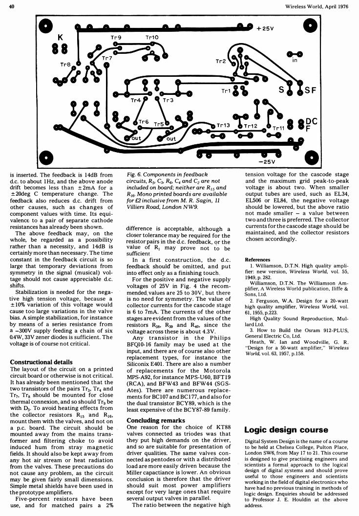
Constructional details The layout of the circuit on a printed circuit board or otherwise is not critical. It has already been mentioned that the two transistors of the pairs Tr3' Tr4 and Tr7' Tr8 should be mounted for close thermal connexion, and so should Trg be with D3. To avoid heating effects from the collector resistors RI5 'and RI6, mount them with the valves, and not on a p.c. board. The circuit should be mounted away from the mains transformer and filtering choke to avoid induced hum from stray magnetic fields. It should also be kept away from any hot air stream or heat radiation from the valves. These precautions do not cause any problem, as the circuit may be given fairly small dimensions. Simple metal shields have been used in the prototype amplifiers.
Five-percent resistors have been use, and for matched pairs a 2%
Fig. 6. Components in feedback circuits, Rs> C3, Rs. C4 and C2 are not included on board; neither are R15 and R16. Mono printed boards are available for £2 inclusive from M. R. Sag in, 11 . Villiers Road, London NW9.
difference is acceptable, although a closer tolerance may be required for the resistor pairs in the d.c. feedback, or the value of RI may prove not t
·o be
sufficient In a first construction, the d.c.
feedback should be omitted, and put into effect only as a finishing touch.
For the positive and negative supply voltages of 25V in Fig. 4 the recommended. values are 25 to 30V, but there is no need for symmetry. The value of collector currents for the cascode stage is 6 to 7mA. The currents of the other stages are evident from the values of the resistors R38, R39 and R4o, since the voltage across these is about 4.3V.
Any transistor in the Phili p s BFQIO-16 family may b e used a t the input, and there are of course also other replacement types, for instance the Siliconix E401. There are also a number of replacements for the M otorola MPS-A92, for instance M PS-U60, BFTl9 (RCA), and BFW43 and BFW44 (SGSAtes). There are numerous replacements for BC 107 and BC I77, and also for the dual transistor BCY89, which is the least expensive of the BCY87-89 family.
Concluding remarks One reason for the choice of KT88 valves connected as triodes was that they put high demands on the driver, and so are suitable for presentation of driver qualities. The same valves connected as pentodes or with a distributed load are more easily driven because the Miller capactiance is lower. An obvious conclusion is therefore that the driver should suit most power amplifiers except for very large ones that require several output valves in parallel.
The ratio between the negative high
•
Wireless World, April 1976
+25V o
SF
• • -25V o
tension voltage for the cascode stage i;lnd the maximum grid peak-to-peak voltage is about two. When smaller· output tubes are used, such as EL 34, EL506 or EL84, the negative voltage should be lowered, but the above ratio not made smaller - a value between two and three is preferred. The collector currents for the cas code stage should be maintained, and the collector resistors chosen accordingly.
References I. Williamson, D.T.N. High quality ampli
fier: new version, Wireless World, vo!. 55, 1949, p. 282.
Williamson, D.T.N. The WiIliamson Amplifier, A Wireless World publication, Iliffe & Sons, Ltd.
2. Ferguson, W.A. Design for a 20-watt high quality amplifier, Wireless World, vo!. 61, 1955, p.223.
High Quality Sound Reproduction, Mullard Ltd.
3. How to Build the Osram 912-PLUS, General Electric Co, Ltd.
Heath, W. ran and Woodville, G. R. "Design for a 50-watt amplifier," Wireless World, vo!. 63, 1957, p.158.
Logic design course Digital System Design is the name of a course to be held at Chelsea College, Pulton Place, London SW6, from May 17 to 21. This course is designed to give practising engineers and scientists a formal approach to the logical design of digital .s�;stems and should prove useful to those engineers and scientists working in the field of digital electronics who have had no previous training in methods of logic design. Enquiries should be addressed to Professor J. E. Houldin at the above address.