Embed Size (px)
Citation preview

331 Week 12.1 Spring 2005
14:332:331Computer Architecture and Assembly Language
Spring 2005
Week 12Buses and I/O system
[Adapted from Dave Patterson’s UCB CS152 slides and
Mary Jane Irwin’s PSU CSE331 slides]

331 Week 12.2 Spring 2005
Head’s Up This week’s material
Buses: Connecting I/O devices- Reading assignment – PH 8.4
Memory hierarchies- Reading assignment – PH 7.1 and B.8-9
Reminders Next week’s material Basics of caches
- Reading assignment – PH 7.2

331 Week 12.3 Spring 2005
Review: Major Components of a Computer
Processor
Control
Datapath
Memory
Devices
Input
Output
Cach
e
Main
M
emo
ry
Seco
nd
ary M
emo
ry(D
isk)
331 Week 12.4 Spring 2005
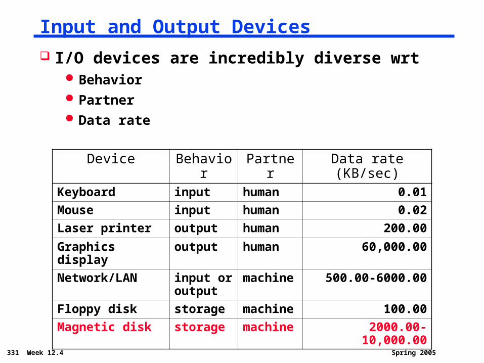
Input and Output Devices
I/O devices are incredibly diverse wrt Behavior Partner Data rate
Device Behavior Partner Data rate (KB/sec)Keyboard input human 0.01
Mouse input human 0.02
Laser printer output human 200.00
Graphics display output human 60,000.00
Network/LAN input or output
machine 500.00-6000.00
Floppy disk storage machine 100.00
Magnetic disk storage machine 2000.00-10,000.00

331 Week 12.5 Spring 2005
Magnetic Disk
Purpose Long term, nonvolatile storage Lowest level in the memory hierarchy
- slow, large, inexpensive
General structure A rotating platter coated with a magnetic surface
Use a moveable read/write head to access the disk
Advantages of hard disks over floppy disks Platters are more rigid (metal or glass) so they can be larger Higher density because it can be controlled more precisely Higher data rate because it spins faster Can incorporate more than one platter

331 Week 12.6 Spring 2005
Organization of a Magnetic Disk
Typical numbers (depending on the disk size) 1 to 15 (2 surface) platters per disk with 1” to 8” diameter 1,000 to 5,000 tracks per surface 63 to 256 sectors per track
- the smallest unit that can be read/written (typically 512 to 1,024 B)
Traditionally all tracks have the same number of sectors- Newer disks with smart controllers can record more sectors on
the outer tracks (constant bit density)
Platters
Track
Sector
331 Week 12.7 Spring 2005
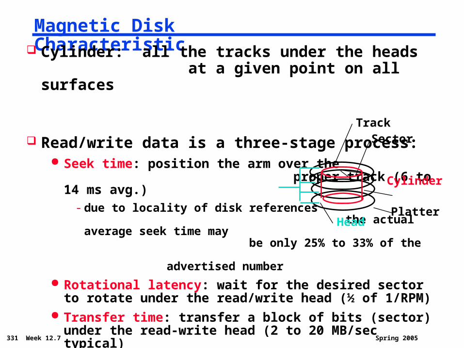
Magnetic Disk Characteristic Cylinder: all the tracks under the heads
at a given point on all surfaces
Read/write data is a three-stage process: Seek time: position the arm over the
proper track (6 to 14 ms avg.)- due to locality of disk references
the actual average seek time may be only 25% to 33% of the advertised number
Rotational latency: wait for the desired sectorto rotate under the read/write head (½ of 1/RPM)
Transfer time: transfer a block of bits (sector)under the read-write head (2 to 20 MB/sec typical)
Controller time: the overhead the disk controller imposes in performing an disk I/O access (typically < 2 ms)
SectorTrack
Cylinder
HeadPlatter

331 Week 12.8 Spring 2005
Magnetic Disk Examples
Characteristic Sun X6713A Toshiba MK2016Disk diameter (inches) 3.5 2.5
Capacity 73 GB 20 GB
MTTF (k hr’s) 1,200 300
# of platters - heads 2 - 4
# cylinders 16,383
# B/sector - # sectors/track 512 - 63
Rotation speed (RPM) 10,000 4,200
Max. - Avg. seek time (ms) ? - 6.6 24 - 13
Avg. rot. latency (ms) 3 7.14
Transfer rate (PIO) 35 MB/sec 16.6 MB/sec
Power (watts) < 2.5
Volume (in3) 4.01
Weight (oz) 3.49
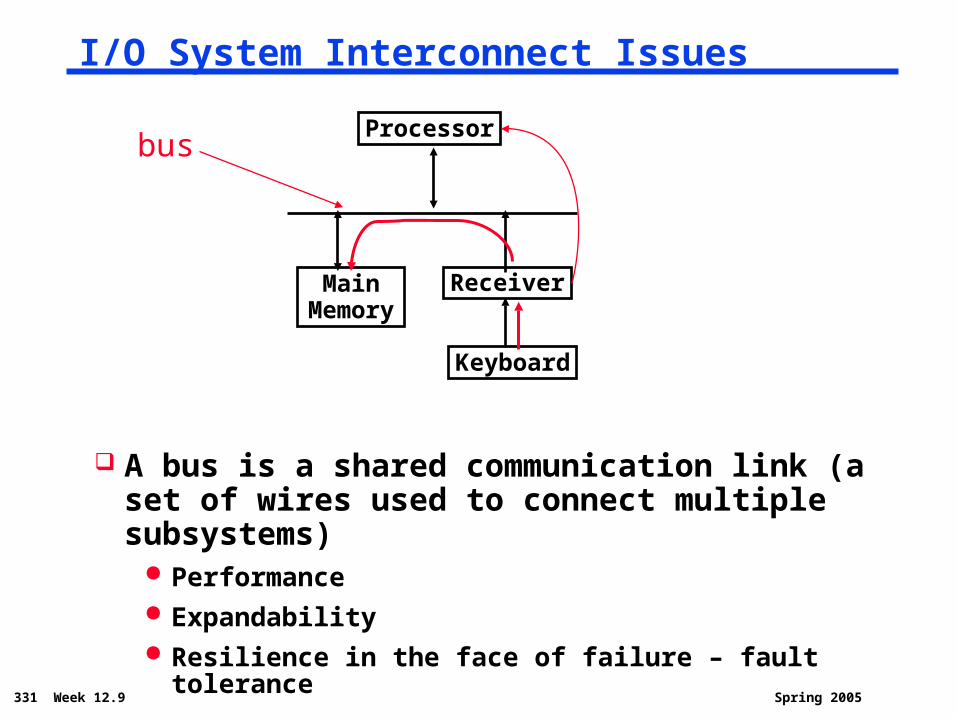
331 Week 12.9 Spring 2005
I/O System Interconnect Issues
A bus is a shared communication link (a set of wires used to connect multiple subsystems)
Performance Expandability Resilience in the face of failure – fault tolerance
Processor
ReceiverMainMemory
Keyboard
bus
331 Week 12.10 Spring 2005
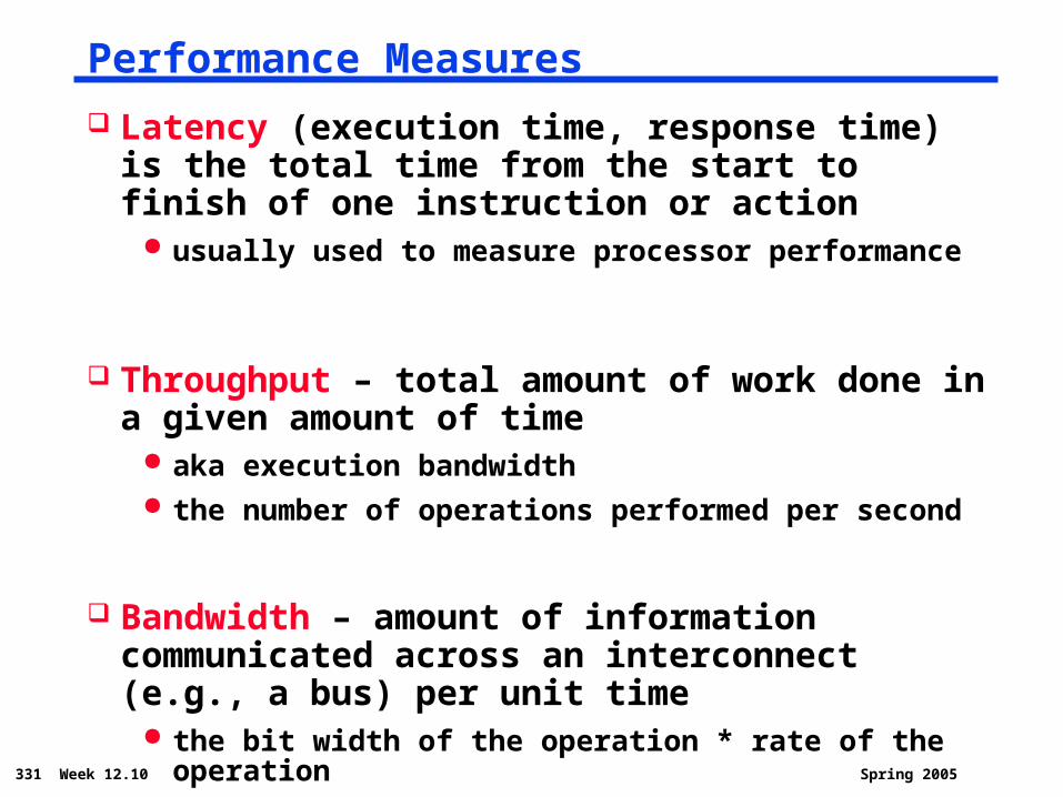
Performance Measures
Latency (execution time, response time) is the total time from the start to finish of one instruction or action
usually used to measure processor performance
Throughput – total amount of work done in a given amount of time
aka execution bandwidth the number of operations performed per second
Bandwidth – amount of information communicated across an interconnect (e.g., a bus) per unit time
the bit width of the operation * rate of the operation usually used to measure I/O performance

331 Week 12.11 Spring 2005
I/O System Expandability
Cache Memory
Memory - I/O Bus
MainMemory
I/OController
Disk Disk
I/OController
I/OController
Terminal Network
interrupt signals
Usually have more than one I/O device in the system each I/O device is controlled by an I/O Controller
Processor
331 Week 12.12 Spring 2005
Quiz
What is disk seek time, and what is rotational time?

331 Week 12.13 Spring 2005
Bus Characteristics
Control lines Signal requests and acknowledgments Indicate what type of information is on the data lines
Data lines Data, complex commands, and addresses
Bus transaction consists of Sending the address Receiving (or sending) the data
Data Lines
Control Lines

331 Week 12.14 Spring 2005
Output (Read) Bus Transaction Defined by what they do to memory
read = output: transfers data from memory (read) to I/O device (write)
Processor Main Memory
Control
Data
Step 1: Processor sends read request and read address to memory
Processor
Control
DataMain Memory
Step 2: Memory accesses data
Processor
Control
DataMain Memory
Step 3: Memory transfers data to disk

331 Week 12.15 Spring 2005
Input (Write) Bus Transaction Defined by what they do to memory
write = input: transfers data from I/O device (read) to memory (write)
Processor Main Memory
Control
Data
Step 1: Processor sends write request and write address to memory
Processor
Control
DataMain Memory
Step 2: Disk transfers data to memory

331 Week 12.16 Spring 2005
Advantages and Disadvantages of Buses Advantages
Versatility:- New devices can be added easily
- Peripherals can be moved between computer systems that use the same bus standard
Low Cost:- A single set of wires is shared in multiple ways
Disadvantages It creates a communication bottleneck
- The bus bandwidth limits the maximum I/O throughput
The maximum bus speed is largely limited by- The length of the bus
- The number of devices on the bus
It needs to support a range of devices with widely varying latencies and data transfer rates
331 Week 12.17 Spring 2005
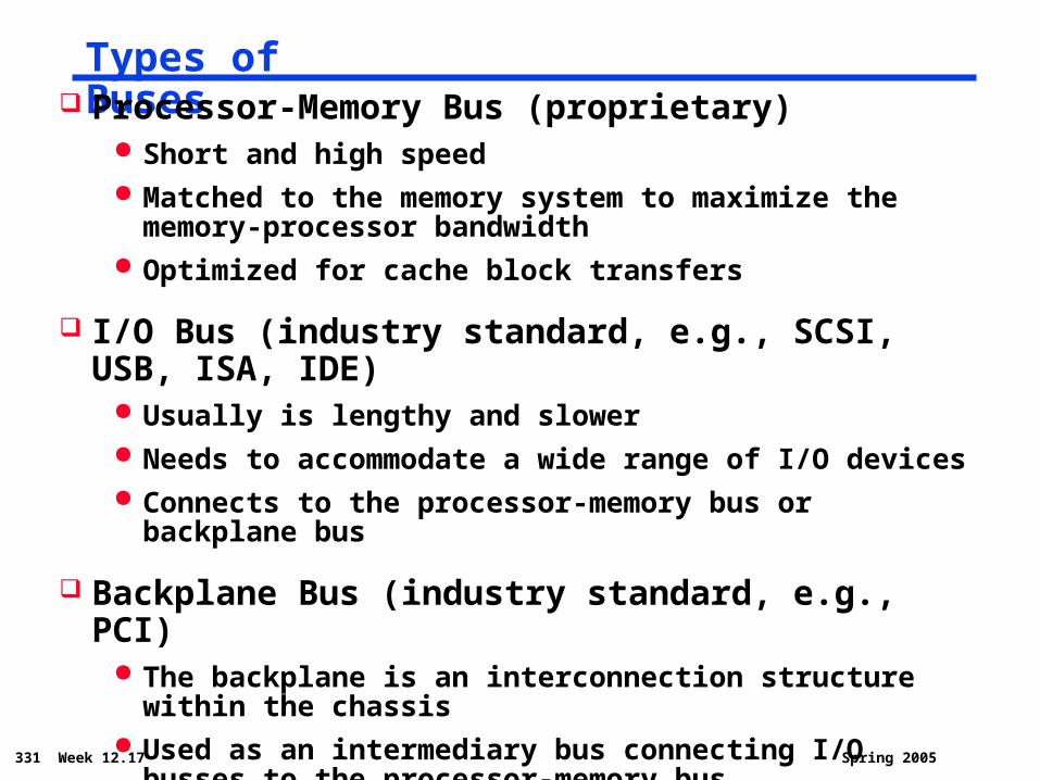
Types of Buses Processor-Memory Bus (proprietary)
Short and high speed Matched to the memory system to maximize the memory-
processor bandwidth Optimized for cache block transfers
I/O Bus (industry standard, e.g., SCSI, USB, ISA, IDE) Usually is lengthy and slower Needs to accommodate a wide range of I/O devices Connects to the processor-memory bus or backplane bus
Backplane Bus (industry standard, e.g., PCI) The backplane is an interconnection structure within the
chassis Used as an intermediary bus connecting I/O busses to the
processor-memory bus

331 Week 12.18 Spring 2005
A Two Bus System
I/O buses tap into the processor-memory bus via Bus Adaptors (that do speed matching between buses)
Processor-memory bus: mainly for processor-memory traffic
I/O busses: provide expansion slots for I/O devices
Processor Memory
Processor-Memory Bus
I/OBus
BusAdaptor
BusAdaptor
BusAdaptor
I/OBus
I/OBus
331 Week 12.19 Spring 2005
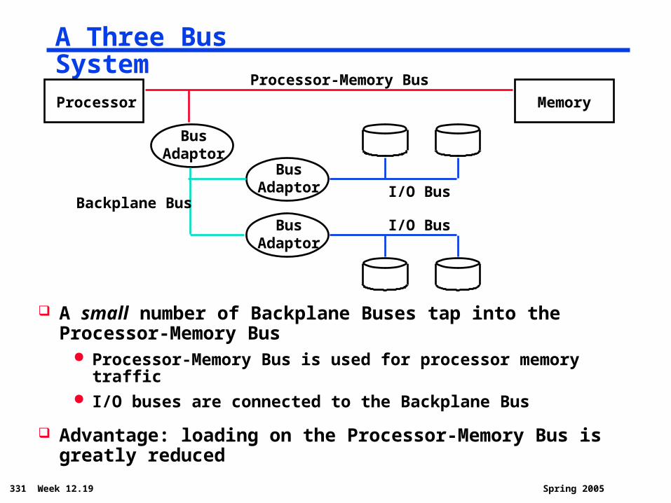
A Three Bus System
A small number of Backplane Buses tap into the Processor-Memory Bus
Processor-Memory Bus is used for processor memory traffic I/O buses are connected to the Backplane Bus
Advantage: loading on the Processor-Memory Bus is greatly reduced
Processor Memory
Processor-Memory Bus
BusAdaptor
Backplane Bus
BusAdaptor
BusAdaptor
I/O Bus
I/O Bus

331 Week 12.20 Spring 2005
I/O System Example (Apple Mac 7200)
Cache Memory
PCI
MainMemory
I/OController
I/OController
Graphic Terminal
Network
Processor
Typical of midrange to high-end desktop system in 1997
PCIInterface/Memory
ControllerI/O
ControllerI/O
Controller
SC
SI
bu
s
Disk
CDRom
Tape
Processor-Memory Bus
Serial portsAudio I/O
331 Week 12.21 Spring 2005
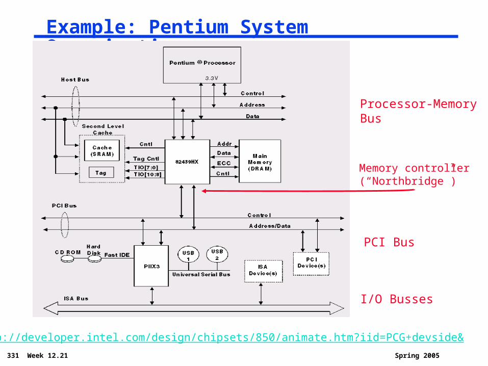
Example: Pentium System Organization
Processor-MemoryBus
PCI Bus
I/O Busses
Memory controller(“Northbridge”)
http://developer.intel.com/design/chipsets/850/animate.htm?iid=PCG+devside&

331 Week 12.22 Spring 2005
Synchronous and Asynchronous Buses Synchronous Bus
Includes a clock in the control lines A fixed protocol for communication that is relative to the clock Advantage: involves very little logic and can run very fast Disadvantages:
- Every device on the bus must run at the same clock rate
- To avoid clock skew, they cannot be long if they are fast
Asynchronous Bus It is not clocked, so requires handshaking protocol (req, ack)
- Implemented with additional control lines
Advantages:- Can accommodate a wide range of devices
- Can be lengthened without worrying about clock skew or synchronization problems
Disadvantage: slow(er)

331 Week 12.23 Spring 2005
Asynchronous Handshaking Protocol
1. Memory sees ReadReq, reads addr from data lines, and raises Ack
2. I/O device sees Ack and releases the ReadReq and data lines
3. Memory sees ReadReq go low and drops Ack
4. When memory has data ready, it places it on data lines and raises DataRdy
5. I/O device sees DataRdy, reads the data from data lines, and raises Ack
6. Memory sees Ack, releases the data lines, and drops DataRdy
7. I/O device sees DataRdy go low and drops Ack
Output (read) data from memory to an I/O device.
I/O device signals a request by raising ReadReq and putting the addr on the data lines
12
3
ReadReq
Data
Ack
DataRdy
addr data
4
5
6
7

331 Week 12.24 Spring 2005
Key Characteristics of Two Bus Standards
Characteristic Firewire (1394) USB 2.0Type I/O I/O
Data bus width(signals)
4 2
Clocking asynchronous asynchronous
Theoretical Peak bandwidth
50 MB/sec (Firewire 400) or 100 MB/sec
(Firewire 800)
0.2 MB/sec (low speed), 1.5 MB/sec (full) or 60MB/sec (high)
Hot plugable Yes yes
Max. devices 63 127
Max. length (copper wire)
4.5 meters 5 meters

331 Week 12.25 Spring 2005
Review: Major Components of a Computer
Processor
Control
Datapath
Memory
Devices
Input
Output

331 Week 12.26 Spring 2005
SecondLevelCache
(SRAM)
A Typical Memory Hierarchy
Control
Datapath
SecondaryMemory(Disk)
On-Chip Components
RegF
ile
MainMemory(DRAM)
Data
Cache
InstrC
ache
ITLB
DT
LB
eDRAM
Speed (ns): .1’s 1’s 10’s 100’s 1,000’s
Size (bytes): 100’s K’s 10K’s M’s T’s
Cost: highest lowest
By taking advantage of the principle of locality: Present the user with as much memory as is available in the
cheapest technology. Provide access at the speed offered by the fastest technology.

331 Week 12.27 Spring 2005
Characteristics of the Memory Hierarchy
Increasing distance from the processor in access time
L1$
L2$
Main Memory
Secondary Memory
Processor
(Relative) size of the memory at each level
Inclusive– what is in L1$ is a subset of what is in L2$ is a subset of what is in MM that is a subset of is in SM
4-8 bytes (word)
1 block
1,023+ bytes (disk sector = page)
8-32 bytes (block)

331 Week 12.28 Spring 2005
Memory Hierarchy Technologies Random Access
“Random” is good: access time is the same for all locations DRAM: Dynamic Random Access Memory
- High density (1 transistor cells), low power, cheap, slow
- Dynamic: need to be “refreshed” regularly (~ every 8 ms)
SRAM: Static Random Access Memory- Low density (6 transistor cells), high power, expensive, fast
- Static: content will last “forever” (until power turned off)
Size: DRAM/SRAM 4 to 8 Cost/Cycle time: SRAM/DRAM 8 to 16
“Non-so-random” Access Technology Access time varies from location to location and from time to
time (e.g., Disk, CDROM)
331 Week 12.29 Spring 2005
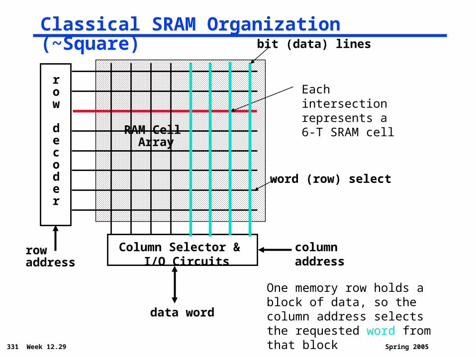
Classical SRAM Organization (~Square)
row
decoder
rowaddress
data word
RAM Cell Array
word (row) select
bit (data) lines
Each intersection represents a 6-T SRAM cell
Column Selector & I/O Circuits
columnaddress
One memory row holds a block of data, so the column address selects the requested word from that block
331 Week 12.30 Spring 2005
data bitdata bit
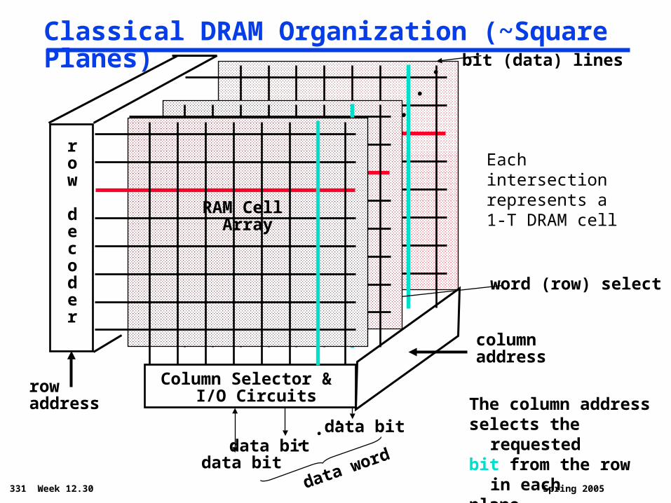
Classical DRAM Organization (~Square Planes)
row
decoder
rowaddress
Column Selector & I/O Circuits
columnaddress
data bit
word (row) select
bit (data) lines
Each intersection represents a 1-T DRAM cell
The column addressselects the requested bit from the row in
eachplanedata word
. . .
. . .
RAM Cell Array

331 Week 12.31 Spring 2005
RAM Memory Definitions Caches use SRAM for speed
Main Memory is DRAM for density Addresses divided into 2 halves (row and column)
- RAS or Row Access Strobe triggering row decoder- CAS or Column Access Strobe triggering column selector
Performance of Main Memory DRAMs Latency: Time to access one word
- Access Time: time between request and when word arrives- Cycle Time: time between requests- Usually cycle time > access time
Bandwidth: How much data can be supplied per unit time- width of the data channel * the rate at which it can be used

331 Week 12.32 Spring 2005
Classical DRAM Operation
DRAM Organization: N rows x N column x M-bit Read or Write M-bit at a time Each M-bit access requires
a RAS / CAS cycle
Row Address
CAS
RAS
Col Address Row Address Col Address
1st M-bit Access 2nd M-bit Access
N r
ows
N cols
DRAM
M bits
RowAddress
ColumnAddress
M-bit OutputCycle Time
331 Week 12.33 Spring 2005
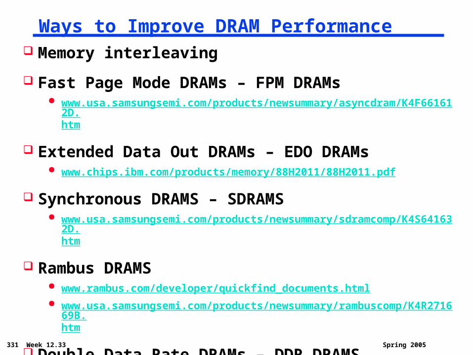
Ways to Improve DRAM Performance Memory interleaving
Fast Page Mode DRAMs – FPM DRAMs www.usa.samsungsemi.com/products/newsummary/asyncdram/K4F661612D.
htm
Extended Data Out DRAMs – EDO DRAMs www.chips.ibm.com/products/memory/88H2011/88H2011.pdf
Synchronous DRAMS – SDRAMS www.usa.samsungsemi.com/products/newsummary/sdramcomp/K4S641632D.
htm
Rambus DRAMS www.rambus.com/developer/quickfind_documents.html www.usa.samsungsemi.com/products/newsummary/rambuscomp/K4R271669B
.htm
Double Data Rate DRAMs – DDR DRAMS www.usa.samsungsemi.com/products/newsummary/ddrsyncdram/K4D62323H
A.htm
. . .
331 Week 12.34 Spring 2005
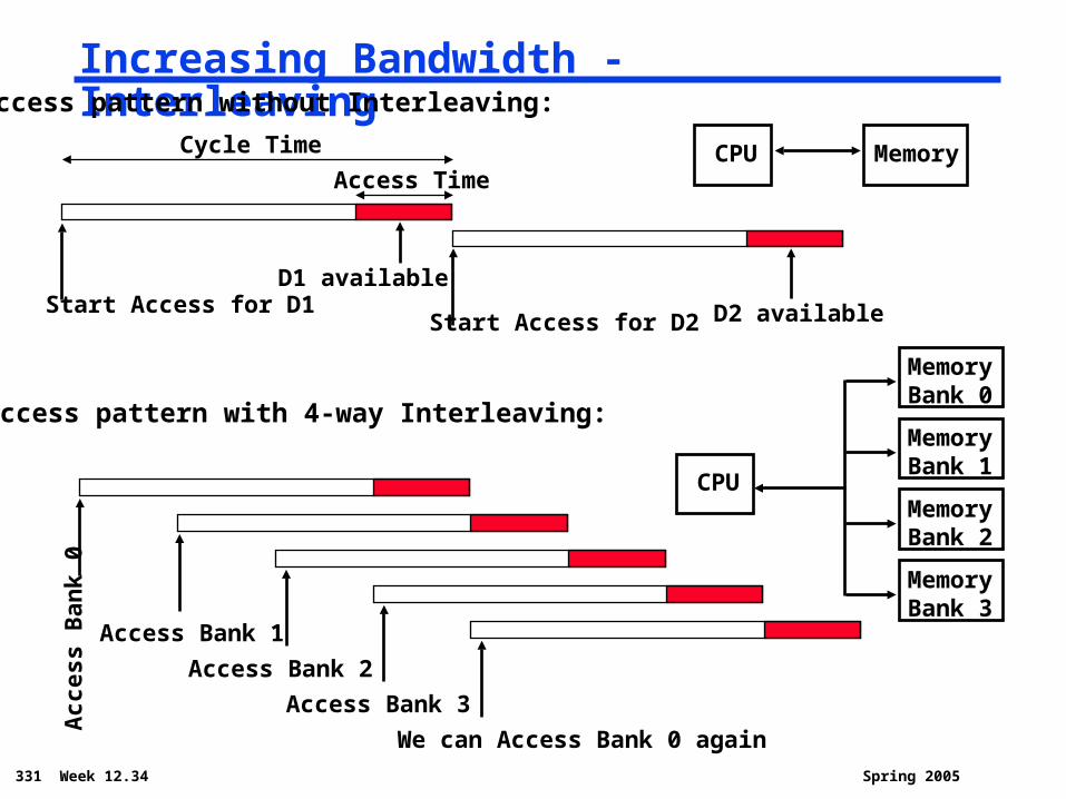
Increasing Bandwidth - InterleavingAccess pattern without Interleaving:
Start Access for D1
CPU Memory
Start Access for D2
D1 available
Access pattern with 4-way Interleaving:
CPU
MemoryBank 1
MemoryBank 0
MemoryBank 3
MemoryBank 2
Cycle Time
Access Time
Acc
ess
Ban
k 0
Access Bank 1
Access Bank 2
Access Bank 3
We can Access Bank 0 again
D2 available

331 Week 12.35 Spring 2005
Problems with Interleaving
How many banks? Ideally, the number of banks number of clocks we have to
wait to access the next word in the bank Only works for sequential accesses (i.e., first word requested
in first bank, second word requested in second bank, etc.)
Increasing DRAM sizes => fewer chips => harder to have banks
Growth bits/chip DRAM : 50%-60%/yr
Only can use for very large memory systems (e.g., those encountered in supercomputer systems)

331 Week 12.36 Spring 2005
N r
ows
N cols
DRAM
ColumnAddress
M-bit Output
M bitsN x M “SRAM”
RowAddress
Fast Page Mode DRAM Operation Fast Page Mode DRAM
N x M “SRAM” to save a row
Row Address
CAS
RAS
Col Address Col Address
1st M-bit Access
Col Address Col Address
2nd M-bit 3rd M-bit 4th M-bit
After a row is read into the SRAM “register”
Only CAS is needed to access other M-bit blocks on that row
RAS remains asserted while CAS is toggled

331 Week 12.37 Spring 2005
Why Care About the Memory Hierarchy?
1
10
100
1000
1980
1981
1983
1984
1985
1986
1987
1988
1989
1990
1991
1992
1993
1994
1995
1996
1997
1998
1999
2000
DRAM
CPU19
82
Processor-MemoryPerformance Gap:(grows 50% / year)
Per
form
ance
Time
“Moore’s Law”
Processor-DRAM Memory GapµProc60%/year(2X/1.5yr)
DRAM9%/year(2X/10yrs)

331 Week 12.38 Spring 2005
Memory Hierarchy: Goals Fact: Large memories are slow, fast memories are
small
How do we create a memory that gives the illusion of being large, cheap and fast (most of the time)?
by taking advantage of
The Principle of Locality: Programs access a relatively small portion of the address space at any instant of time.
Address Space0 2n - 1
Probabilityof reference

331 Week 12.39 Spring 2005
Memory Hierarchy: Why Does it Work?
Temporal Locality (Locality in Time):=> Keep most recently accessed data items closer to the
processor
Spatial Locality (Locality in Space):=> Move blocks consists of contiguous words to the upper
levels
Lower LevelMemoryUpper Level
MemoryTo Processor
From ProcessorBlk X
Blk Y

331 Week 12.40 Spring 2005
Memory Hierarchy: Terminology Hit: data appears in some block in the upper level (Block X)
Hit Rate: the fraction of memory accesses found in the upper level Hit Time: Time to access the upper level which consists of
RAM access time + Time to determine hit/miss
Miss: data needs to be retrieve from a block in the lower level (Block Y)
Miss Rate = 1 - (Hit Rate) Miss Penalty: Time to replace a block in the upper level
+ Time to deliver the block the processor Hit Time << Miss Penalty
Lower LevelMemoryUpper Level
MemoryTo Processor
From ProcessorBlk X
Blk Y

331 Week 12.41 Spring 2005
How is the Hierarchy Managed? registers <-> memory
by compiler (programmer?)
cache <-> main memory by the hardware
main memory <-> disks by the hardware and operating system (virtual memory) by the programmer (files)

331 Week 12.42 Spring 2005
Summary DRAM is slow but cheap and dense
Good choice for presenting the user with a BIG memory system
SRAM is fast but expensive and not very dense Good choice for providing the user FAST access time
Two different types of locality Temporal Locality (Locality in Time): If an item is referenced, it will
tend to be referenced again soon. Spatial Locality (Locality in Space): If an item is referenced, items
whose addresses are close by tend to be referenced soon.
By taking advantage of the principle of locality: Present the user with as much memory as is available in the
cheapest technology. Provide access at the speed offered by the fastest technology.


![CS35101 Computer Architecture Spring 2006 Week 8 P Durand (durand) [Adapted from MJI (mji)] [Adapted from Dave Patterson’s](https://img.pdfslide.us/doc/110x75/56649eab5503460f94bb0645/cs35101-computer-architecture-spring-2006-week-8-p-durand-wwwcskentedudurand.jpg)