Embed Size (px)
Citation preview
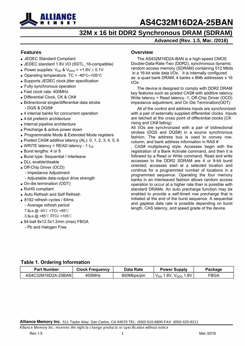
32M x 16 bit DDR2 Synchronous DRAM (SDRAM) Advanced (Rev. 1.5, Mar. /2016)
Features • JEDEC Standard Compliant• JEDEC standard 1.8V I/O (SSTL_18-compatible)• Power supplies: VDD & VDDQ = +1.8V ± 0.1V• Operating temperature: TC = -40~105• Supports JEDEC clock jitter specification• Fully synchronous operation• Fast clock rate: 400MHz• Differential Clock, CK & CK#• Bidirectional single/differential data strobe
- DQS & DQS#• 4 internal banks for concurrent operation• 4-bit prefetch architecture• Internal pipeline architecture• Precharge & active power down• Programmable Mode & Extended Mode registers• Posted CAS# additive latency (AL): 0, 1, 2, 3, 4, 5, 6• WRITE latency = READ latency - 1 tCK
• Burst lengths: 4 or 8• Burst type: Sequential / Interleave• DLL enable/disable• Off-Chip Driver (OCD)
- Impedance Adjustment- Adjustable data-output drive strength
• On-die termination (ODT)• RoHS compliant• Auto Refresh and Self Refresh• 8192 refresh cycles / 64ms
- Average refresh period7.8µs @ -40 ≦TC≦ +853.9µs @ +85 <TC≦ +105
• 84-ball 8x12.5x1.2mm (max) FBGA- Pb and Halogen Free
Overview The AS432M16D2A-BAN is a high-speed CMOS
Double-Data-Rate-Two (DDR2), synchronous dynamic random access memory (SDRAM) containing 512 Mbits in a 16-bit wide data I/Os. It is internally configured as a quad bank DRAM, 4 banks x 8Mb addresses x 16 I/Os
The device is designed to comply with DDR2 DRAM key features such as posted CAS# with additive latency, Write latency = Read latency -1, Off-Chip Driver (OCD) impedance adjustment, and On Die Termination(ODT).
All of the control and address inputs are synchronized with a pair of externally supplied differential clocks. Inputs are latched at the cross point of differential clocks (CK rising and CK# falling) All I/Os are synchronized with a pair of bidirectional strobes (DQS and DQS#) in a source synchronous fashion. The address bus is used to convey row, column, and bank address information in RAS # , CAS# multiplexing style. Accesses begin with the registration of a Bank Activate command, and then it is followed by a Read or Write command. Read and write accesses to the DDR2 SDRAM are 4 or 8-bit burst oriented; accesses start at a selected location and continue for a programmed number of locations in a programmed sequence. Operating the four memory banks in an interleaved fashion allows random access operation to occur at a higher rate than is possible with standard DRAMs. An auto precharge function may be enabled to provide a self-timed row precharge that is initiated at the end of the burst sequence. A sequential and gapless data rate is possible depending on burst length, CAS latency, and speed grade of the device.
AS4C32M16D2A-25BAN
Alliance Memory Inc. 511 Taylor Way, San Carlos, CA 94070 TEL: (650) 610-6800 FAX: (650) 620-9211
Alliance Memory Inc. reserves the right to change products or specification without noticeRev.1.5 1 Mar./2016
Table 1. Ordering Information Part Number Clock Frequency Data Rate Power Supply Package
AS4C32M16D2A-25BAN 400MHz 800Mbps/pin VDD 1.8V, VDDQ 1.8V FBGA
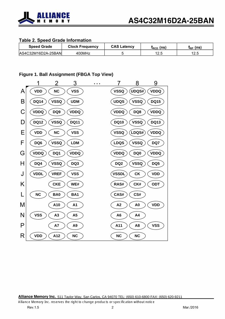
Figure 1. Ball Assignment (FBGA Top View)
A
B
C
D
E
1 2 3 7 8 9VDD NC
DQ14 VSSQ
VDDQ DQ9
DQ12 VSSQ
VDD NC
VSS
UDM
VDDQ
DQ11
VSS
.
VSSQ UDQS#
UDQS VSSQ
VDDQ DQ8
DQ10 VSSQ
VSSQ LDQS#
VDDQ
DQ15
VDDQ
DQ13
VDDQ
F DQ6 VSSQ LDM LDQS VSSQ DQ7
G VDDQ DQ1 VDDQ VDDQ DQ0 VDDQ
H DQ4 VSSQ DQ3 DQ2 VSSQ DQ5
J VDDL VREF VSS VSSDL CK VDD
K CKE WE# RAS# CK# ODT
L NC BA0 BA1 CAS# CS#
M A10 A1 A2 A0 VDD
N VSS A3 A5 A6 A4
P A7 A9 A11 A8 VSS
R VDD A12 NC NC NC
AS4C32M16D2A-25BAN
Alliance Memory Inc. 511 Taylor Way, San Carlos, CA 94070 TEL: (650) 610-6800 FAX: (650) 620-9211
Alliance Memory Inc. reserves the right to change products or specification without noticeRev.1.5 2 Mar./2016
Table 2. Speed Grade Information Speed Grade Clock Frequency CAS Latency tRCD (ns) tRP (ns)
AS4C32M16D2A-25BAN 400MHz 5 12.5 12.5
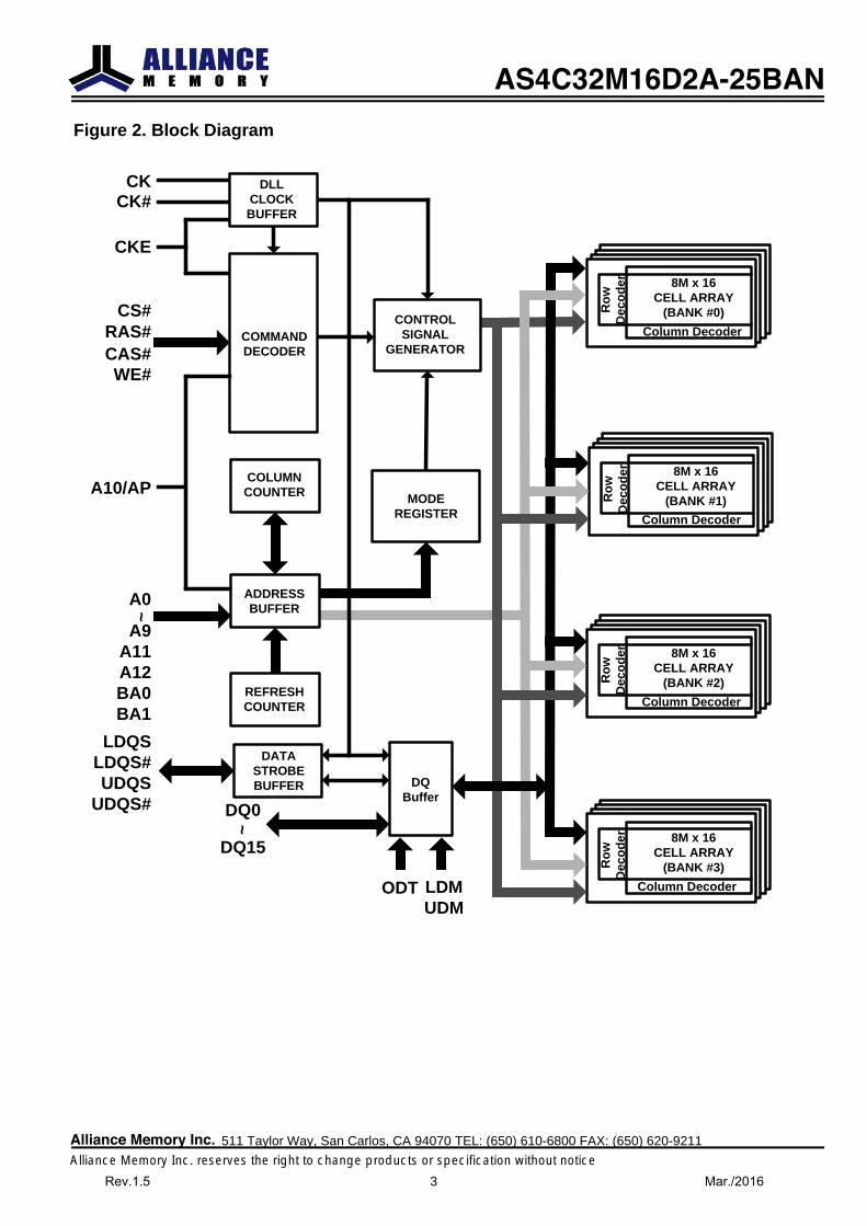
Figure 2. Block Diagram
CK#
CKE
CS#RAS#CAS#WE#
DLLCLOCKBUFFER
COMMANDDECODER
COLUMNCOUNTER
CONTROLSIGNAL
GENERATOR
ADDRESSBUFFER
REFRESHCOUNTER
8M x 16CELL ARRAY
(BANK #0)Row
D
ecod
er
8M x 16CELL ARRAY
(BANK #1)Row
D
ecod
er
8M x 16CELL ARRAY
(BANK #2)Row
D
ecod
er
8M x 16CELL ARRAY
(BANK #3)Row
D
ecod
er
Column Decoder
Column Decoder
Column Decoder
Column Decoder
MODEREGISTER
A10/AP
A9A11A12BA0BA1
A0
CK
DATASTROBEBUFFER
LDQSLDQS#UDQS
UDQS#DQ
Buffer
LDMUDM
DQ15
DQ0~
ODT
~
AS4C32M16D2A-25BAN
Alliance Memory Inc. 511 Taylor Way, San Carlos, CA 94070 TEL: (650) 610-6800 FAX: (650) 620-9211
Alliance Memory Inc. reserves the right to change products or specification without noticeRev.1.5 3 Mar./2016
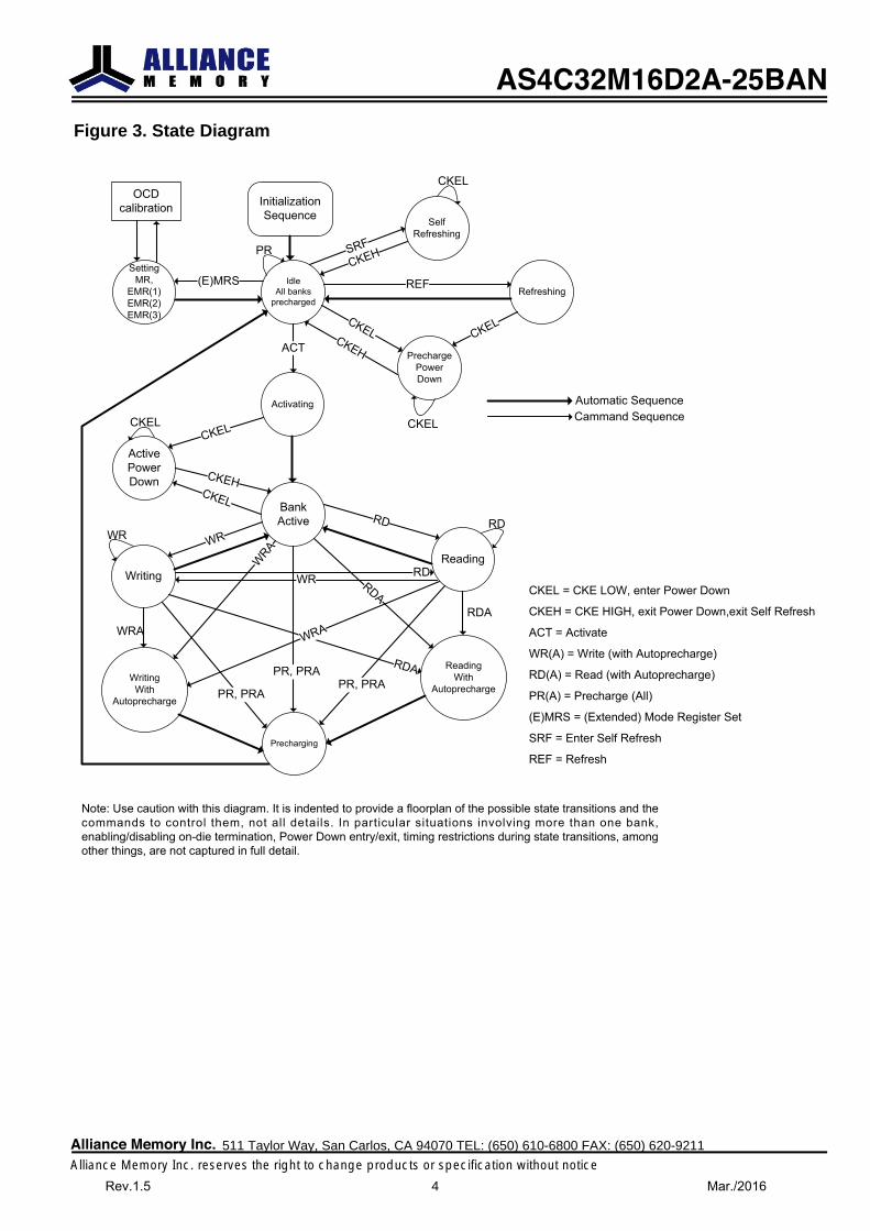
Figure 3. State Diagram
(E)MRSSetting
MR, EMR(1)EMR(2)EMR(3)
OCDcalibration Initialization
Sequence
IdleAll banks
precharged
SelfRefreshing
Refreshing
PrechargePowerDown
Activating
ActivePowerDown
BankActive
Writing
WritingWith
Autoprecharge
Precharging
ReadingWith
Autoprecharge
Reading
ACT
CKEL
CKEHCKEL
WR
RDA
RDA
WRA
WRA
WR RD
RD
PR, PRAPR, PRA
PR, PRA
RDAWRA
CKELCKEH
CKEL
SRFCKEH
REF
CKEL
WRRD
PR
CKEL
CKEL
Automatic SequenceCammand Sequence
CKEL = CKE LOW, enter Power Down
CKEH = CKE HIGH, exit Power Down,exit Self Refresh
ACT = Activate
WR(A) = Write (with Autoprecharge)
RD(A) = Read (with Autoprecharge)
PR(A) = Precharge (All)
(E)MRS = (Extended) Mode Register Set
SRF = Enter Self Refresh
REF = Refresh
Note: Use caution with this diagram. It is indented to provide a floorplan of the possible state transitions and the commands to control them, not all details. In particular situations involving more than one bank, enabling/disabling on-die termination, Power Down entry/exit, timing restrictions during state transitions, among other things, are not captured in full detail.
AS4C32M16D2A-25BAN
Alliance Memory Inc. 511 Taylor Way, San Carlos, CA 94070 TEL: (650) 610-6800 FAX: (650) 620-9211
Alliance Memory Inc. reserves the right to change products or specification without noticeRev.1.5 4 Mar./2016
Ball Descriptions Table 3. Ball Descriptions
Symbol Type Description
CK, CK# Input Differential Clock: CK, CK# are driven by the system clock. All SDRAM input signals are sampled on the crossing of positive edge of CK and negative edge of CK#. Output (Read) data is referenced to the crossings of CK and CK# (both directions of crossing).
CKE Input Clock Enable: CKE activates (HIGH) and deactivates (LOW) the CK signal. If CKE goes LOW synchronously with clock, the internal clock is suspended from the next clock cycle and the state of output and burst address is frozen as long as the CKE remains LOW. When all banks are in the idle state, deactivating the clock controls the entry to the Power Down and Self Refresh modes.
BA0, BA1 Input Bank Address: BA0 and BA1 define to which bank the BankActivate, Read, Write, or BankPrecharge command is being applied.
A0-A12 Input Address Inputs: A0-A12 are sampled during the BankActivate command (row address A0-A12) and Read/Write command (column address A0-A9 with A10 defining Auto Precharge).
CS# Input Chip Select: CS# enables (sampled LOW) and disables (sampled HIGH) the command decoder. All commands are masked when CS# is sampled HIGH. CS#provides for external bank selection on systems with multiple banks. It is considered part of the command code.
RAS# Input Row Address Strobe: The RAS# signal defines the operation commands in conjunction with the CAS# and WE# signals and is latched at the crossing of positive edges of CK and negative edge of CK#. When RAS# and CS# are asserted "LOW" and CAS# is asserted "HIGH," either the BankActivate command or the Precharge command is selected by the WE# signal. When the WE# is asserted "HIGH," the BankActivate command is selected and the bank designated by BA is turned on to the active state. When the WE# is asserted "LOW," the Precharge command is selected and the bank designated by BA is switched to the idle state after the precharge operation.
CAS# Input Column Address Strobe: The CAS# signal defines the operation commands inconjunction with the RAS# and WE# signals and is latched at the crossing of positive edges of CK and negative edge of CK#. When RAS# is held "HIGH" and CS# is asserted "LOW," the column access is started by asserting CAS# "LOW." Then, the Read or Write command is selected by asserting WE# “HIGH " or “LOW".
WE# Input Write Enable: The WE# signal defines the operation commands in conjunction with the RAS# and CAS# signals and is latched at the crossing of positive edges of CKand negative edge of CK#. The WE# input is used to select the BankActivate or Precharge command and Read or Write command.
LDQS,
LDQS#
UDQS
UDQS#
Input /
Output
Bidirectional Data Strobe: Specifies timing for Input and Output data. Read Data Strobe is edge triggered. Write Data Strobe provides a setup and hold time for data and DQM. LDQS is for DQ0~7, UDQS is for DQ8~15. The data strobes LDOS and UDQS may be used in single ended mode or paired with LDQS# and UDQS# to provide differential pair signaling to the system during both reads and writes.A control bit at EMR (1)[A10] enables or disables all complementary data strobe signals.
LDM,
UDM
Input Data Input Mask: Input data is masked when DM is sampled HIGH during a write cycle. LDM masks DQ0-DQ7, UDM masks DQ8-DQ15.
DQ0 - DQ15 Input / Output
Data I/O: Bi-directional data bus.
AS4C32M16D2A-25BAN
Alliance Memory Inc. 511 Taylor Way, San Carlos, CA 94070 TEL: (650) 610-6800 FAX: (650) 620-9211
Alliance Memory Inc. reserves the right to change products or specification without noticeRev.1.5 5 Mar./2016
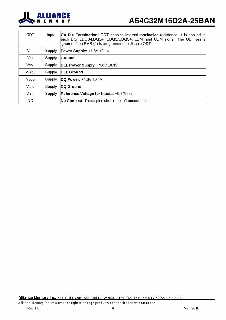
ODT Input On Die Termination: ODT enables internal termination resistance. It is applied to each DQ, LDQS/LDQS#, UDQS/UDQS#, LDM, and UDM signal. The ODT pin is ignored if the EMR (1) is programmed to disable ODT.
VDD Supply Power Supply: +1.8V ±0.1V
VSS Supply Ground
VDDL Supply DLL Power Supply: +1.8V ±0.1V
VSSDL Supply DLL Ground
VDDQ Supply DQ Power: +1.8V ±0.1V.
VSSQ Supply DQ Ground
VREF Supply Reference Voltage for Inputs: +0.5*VDDQ
NC - No Connect: These pins should be left unconnected.
AS4C32M16D2A-25BAN
Alliance Memory Inc. 511 Taylor Way, San Carlos, CA 94070 TEL: (650) 610-6800 FAX: (650) 620-9211
Alliance Memory Inc. reserves the right to change products or specification without noticeRev.1.5 6 Mar./2016
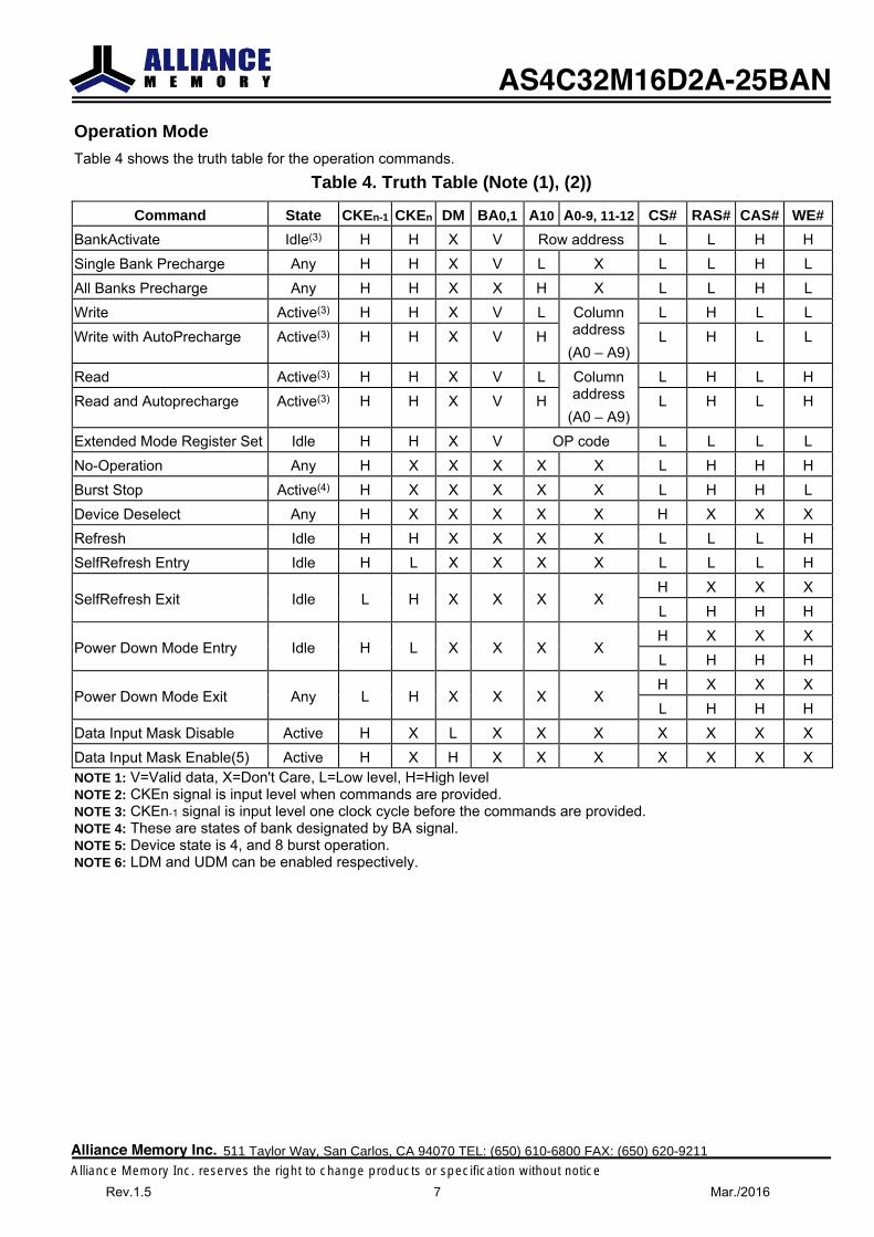
Operation Mode Table 4 shows the truth table for the operation commands.
Table 4. Truth Table (Note (1), (2))
Command State CKEn-1 CKEn DM BA0,1 A10 A0-9, 11-12 CS# RAS# CAS# WE#BankActivate Idle(3) H H X V Row address L L H H Single Bank Precharge Any H H X V L X L L H L All Banks Precharge Any H H X X H X L L H L Write Active(3) H H X V L Column
address (A0 – A9)
L H L L Write with AutoPrecharge Active(3) H H X V H L H L L
Read Active(3) H H X V L Column address
(A0 – A9)
L H L H Read and Autoprecharge Active(3) H H X V H L H L H
Extended Mode Register Set Idle H H X V OP code L L L L No-Operation Any H X X X X X L H H H Burst Stop Active(4) H X X X X X L H H L Device Deselect Any H X X X X X H X X X Refresh Idle H H X X X X L L L H SelfRefresh Entry Idle H L X X X X L L L H
SelfRefresh Exit Idle L H X X X X H X X X L H H H
Power Down Mode Entry Idle H L X X X X H X X X L H H H
Power Down Mode Exit Any L H X X X X H X X X L H H H
Data Input Mask Disable Active H X L X X X X X X X Data Input Mask Enable(5) Active H X H X X X X X X X NOTE 1: V=Valid data, X=Don't Care, L=Low level, H=High level NOTE 2: CKEn signal is input level when commands are provided. NOTE 3: CKEn-1 signal is input level one clock cycle before the commands are provided. NOTE 4: These are states of bank designated by BA signal. NOTE 5: Device state is 4, and 8 burst operation. NOTE 6: LDM and UDM can be enabled respectively.
AS4C32M16D2A-25BAN
Alliance Memory Inc. 511 Taylor Way, San Carlos, CA 94070 TEL: (650) 610-6800 FAX: (650) 620-9211
Alliance Memory Inc. reserves the right to change products or specification without noticeRev.1.5 7 Mar./2016
Functional Description Read and write accesses to the DDR2 SDRAM are burst oriented; accesses start at a selected location and continue for a burst length of four or eight in a programmed sequence. Accesses begin with the registration of an Active command, which is then followed by a Read or Write command. The address bits registered coincident with the active command are used to select the bank and row to be accessed (BA0, BA1 select the bank; A0-A12 select the row). The address bits registered coincident with the Read or Write command are used to select the starting column location for the burst access and to determine if the auto precharge command is to be issued. Prior to normal operation, the DDR2 SDRAM must be initialized. The following sections provide detailed information covering device initialization, register definition, command descriptions, and device operation.
Power-up and Initialization
DDR2 SDRAMs must be powered up and initialized in a predefined manner. Operational procedures other than those specified may result in undefined operation. The following sequence is required for POWER UP and Initialization. 1. Apply power and attempt to maintain CKE below 0.2*VDDQ and ODT *1 at a low state (all other inputs may be
undefined.) The VDD voltage ramp time must be no greater than 200ms from when VDD ramps from 300mV toVDDmin; and during the VDD voltage ramp, |VDD-VDDQ| ≦ 0.3V
- VDD, VDDL and VDDQ are driven from a single power converter output, AND- VTT is limited to 0.95 V max, AND - VREF tracks VDDQ/2. or - Apply VDD before or at the same time as VDDL. - Apply VDDL before or at the same time as VDDQ. - Apply VDDQ before or at the same time as VTT & VREF. At least one of these two sets of conditions must be met.
2. Start clock and maintain stable condition.3. For the minimum of 200µs after stable power and clock (CK, CK#), then apply NOP or deselect and take CKE
HIGH.4. Wait minimum of 400ns then issue precharge all command. NOP or deselect applied during 400ns period.5. Issue EMRS(2) command. (To issue EMRS (2) command, provide “LOW” to BA0, “HIGH” to BA1.)6. Issue EMRS (3) command. (To issue EMRS (3) command, provide “HIGH” to BA0 and BA1.)7. Issue EMRS to enable DLL. (To issue "DLL Enable" command, provide "LOW" to A0, "HIGH" to BA0 and
"LOW" to BA1.)8. Issue a Mode Register Set command for “DLL reset”.
(To issue DLL reset command, provide "HIGH" to A8 and "LOW" to BA0-1)9. Issue precharge all command.
10. Issue 2 or more auto-refresh commands.11. Issue a mode register set command with LOW to A8 to initialize device operation. (i.e. to program operating
parameters without resetting the DLL.)12. At least 200 clocks after step 8, execute OCD Calibration (Off Chip Driver impedance adjustment).If OCD
calibration is not used, EMRS OCD Default command (A9=A8=A7=HIGH) followed by EMRS OCD calibration Mode Exit command (A9=A8=A7=LOW) must be issued with other operating parameters of EMRS.
13. The DDR2 SDRAM is now ready for normal operation.
NOTE 1: To guarantee ODT off, VREF must be valid and a LOW level must be applied to the ODT pin.
AS4C32M16D2A-25BAN
Alliance Memory Inc. 511 Taylor Way, San Carlos, CA 94070 TEL: (650) 610-6800 FAX: (650) 620-9211
Alliance Memory Inc. reserves the right to change products or specification without noticeRev.1.5 8 Mar./2016
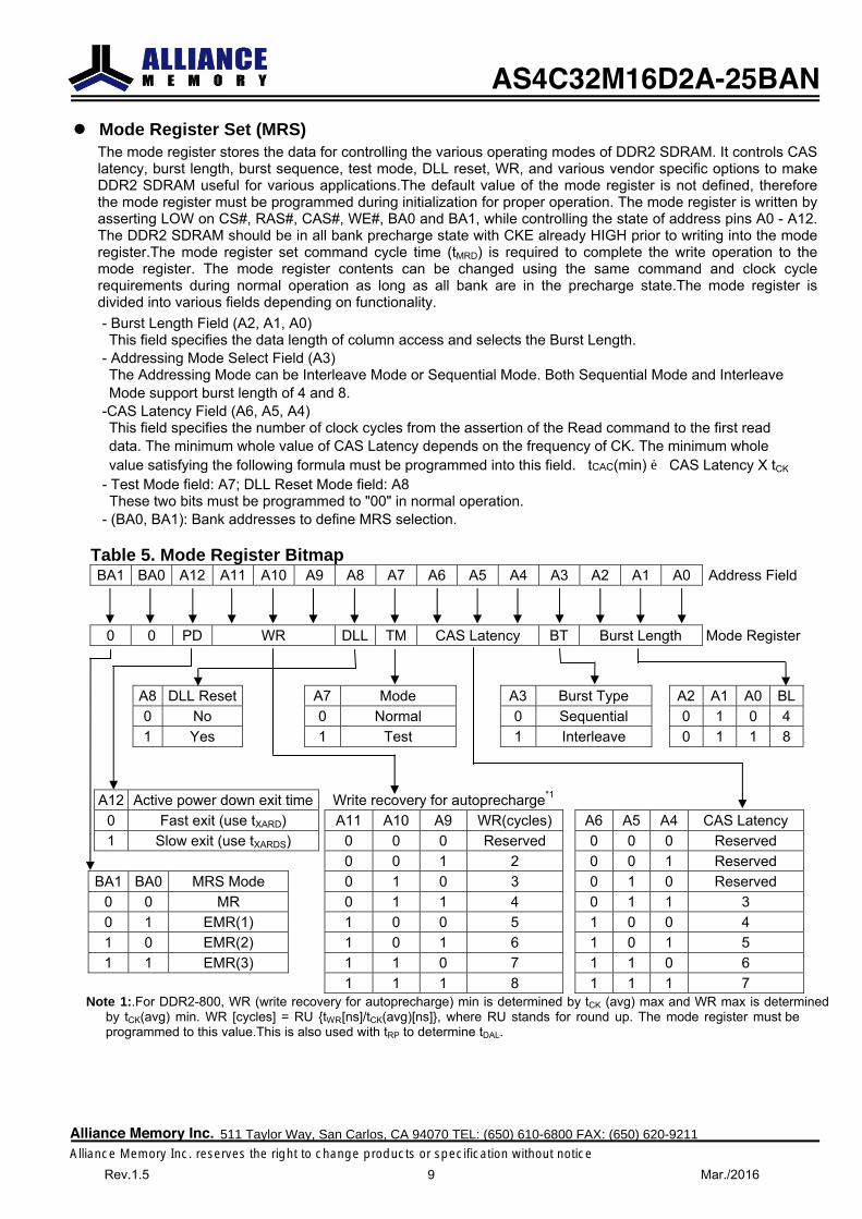
Mode Register Set (MRS) The mode register stores the data for controlling the various operating modes of DDR2 SDRAM. It controls CAS latency, burst length, burst sequence, test mode, DLL reset, WR, and various vendor specific options to make DDR2 SDRAM useful for various applications.The default value of the mode register is not defined, therefore the mode register must be programmed during initialization for proper operation. The mode register is written by asserting LOW on CS#, RAS#, CAS#, WE#, BA0 and BA1, while controlling the state of address pins A0 - A12. The DDR2 SDRAM should be in all bank precharge state with CKE already HIGH prior to writing into the mode register.The mode register set command cycle time (tMRD) is required to complete the write operation to the mode register. The mode register contents can be changed using the same command and clock cycle requirements during normal operation as long as all bank are in the precharge state.The mode register is divided into various fields depending on functionality. - Burst Length Field (A2, A1, A0) This field specifies the data length of column access and selects the Burst Length.
- Addressing Mode Select Field (A3) The Addressing Mode can be Interleave Mode or Sequential Mode. Both Sequential Mode and Interleave Mode support burst length of 4 and 8.
-CAS Latency Field (A6, A5, A4) This field specifies the number of clock cycles from the assertion of the Read command to the first read data. The minimum whole value of CAS Latency depends on the frequency of CK. The minimum whole value satisfying the following formula must be programmed into this field. tCAC(min) ≦ CAS Latency X tCK
- Test Mode field: A7; DLL Reset Mode field: A8 These two bits must be programmed to "00" in normal operation.
- (BA0, BA1): Bank addresses to define MRS selection.
Table 5. Mode Register Bitmap BA1 BA0 A12 A11 A10 A9 A8 A7 A6 A5 A4 A3 A2 A1 A0 Address Field
0 0 PD WR DLL TM CAS Latency BT Burst Length Mode Register
A8 DLL Reset A7 Mode A3 Burst Type A2 A1 A0 BL 0 No 0 Normal 0 Sequential 0 1 0 4 1 Yes 1 Test 1 Interleave 0 1 1 8
Note 1:.For DDR2-800, WR (write recovery for autoprecharge) min is determined by tCK (avg) max and WR max is determined by tCK(avg) min. WR [cycles] = RU tWR[ns]/tCK(avg)[ns], where RU stands for round up. The mode register must be programmed to this value.This is also used with tRP to determine tDAL.
A12 Active power down exit time Write recovery for autoprecharge*1
0 Fast exit (use tXARD) A11 A10 A9 WR(cycles) A6 A5 A4 CAS Latency 1 Slow exit (use tXARDS) 0 0 0 Reserved 0 0 0 Reserved
0 0 1 2 0 0 1 Reserved BA1 BA0 MRS Mode 0 1 0 3 0 1 0 Reserved
0 0 MR 0 1 1 4 0 1 1 3 0 1 EMR(1) 1 0 0 5 1 0 0 41 0 EMR(2) 1 0 1 6 1 0 1 51 1 EMR(3) 1 1 0 7 1 1 0 6
1 1 1 8 1 1 1 7
AS4C32M16D2A-25BAN
Alliance Memory Inc. 511 Taylor Way, San Carlos, CA 94070 TEL: (650) 610-6800 FAX: (650) 620-9211
Alliance Memory Inc. reserves the right to change products or specification without noticeRev.1.5 9 Mar./2016
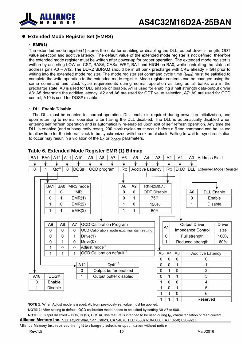
Extended Mode Register Set (EMRS) - EMR(1) The extended mode register(1) stores the data for enabling or disabling the DLL, output driver strength, ODT value selection and additive latency. The default value of the extended mode register is not defined, therefore the extended mode register must be written after power-up for proper operation. The extended mode register is written by asserting LOW on CS#, RAS#, CAS#, WE#, BA1 and HIGH on BA0, while controlling the states of address pins A0 ~ A12. The DDR2 SDRAM should be in all bank precharge with CKE already HIGH prior to writing into the extended mode register. The mode register set command cycle time (tMRD) must be satisfied to complete the write operation to the extended mode register. Mode register contents can be changed using the same command and clock cycle requirements during normal operation as long as all banks are in the precharge state. A0 is used for DLL enable or disable. A1 is used for enabling a half strength data-output driver. A3~A5 determine the additive latency, A2 and A6 are used for ODT value selection, A7~A9 are used for OCD control, A10 is used for DQS# disable.
- DLL Enable/Disable The DLL must be enabled for normal operation. DLL enable is required during power up initialization, and
upon returning to normal operation after having the DLL disabled. The DLL is automatically disabled when entering self refresh operation and is automatically re-enabled upon exit of self refresh operation. Any time the DLL is enabled (and subsequently reset), 200 clock cycles must occur before a Read command can be issued to allow time for the internal clock to be synchronized with the external clock. Failing to wait for synchronization to occur may result in a violation of the tAC or tDQSCK parameters.
Table 6. Extended Mode Register EMR (1) Bitmap BA1 BA0 A12 A11 A10 A9 A8 A7 A6 A5 A4 A3 A2 A1 A0 Address Field
0 1 Qoff 0 DQS# OCD program Rtt Additive Latency Rtt D.I.C DLL Extended Mode Register
BA1 BA0 MRS mode A6 A2 Rtt(NOMINAL)
0 0 MR 0 0 ODT Disable A0 DLL Enable 0 1 EMR(1) 0 1 75Ω 0 Enable 1 0 EMR(2) 1 0 150Ω 1 Disable 1 1 EMR(3) 1 1 50Ω
A9 A8 A7 OCD Calibration Program A1
Output Driver Impedance Control
Driver size 0 0 0 OCD Calibration mode exit; maintain setting
0 0 1 Drive(1) 0 Full strength 100% 0 1 0 Drive(0) 1 Reduced strength 60% 1 0 0 Adjust mode*1 1 1 1 OCD Calibration default*2 A5 A4 A3 Additive Latency
0 0 0 0 A12 Qoff *3 0 0 1 1
0 Output buffer enabled 0 1 0 2 A10 DQS# 1 Output buffer disabled 0 1 1 3
0 Enable 1 0 0 4 1 Disable 1 0 1 5
1 1 0 6 1 1 1 Reserved
NOTE 1: When Adjust mode is issued, AL from previously set value must be applied. NOTE 2: After setting to default, OCD calibration mode needs to be exited by setting A9-A7 to 000. NOTE 3: Output disabled – DQs, DQSs, DQSs#.This feature is intended to be used during IDD characterization of read current.
AS4C32M16D2A-25BAN
Alliance Memory Inc. 511 Taylor Way, San Carlos, CA 94070 TEL: (650) 610-6800 FAX: (650) 620-9211
Alliance Memory Inc. reserves the right to change products or specification without noticeRev.1.5 10 Mar./2016
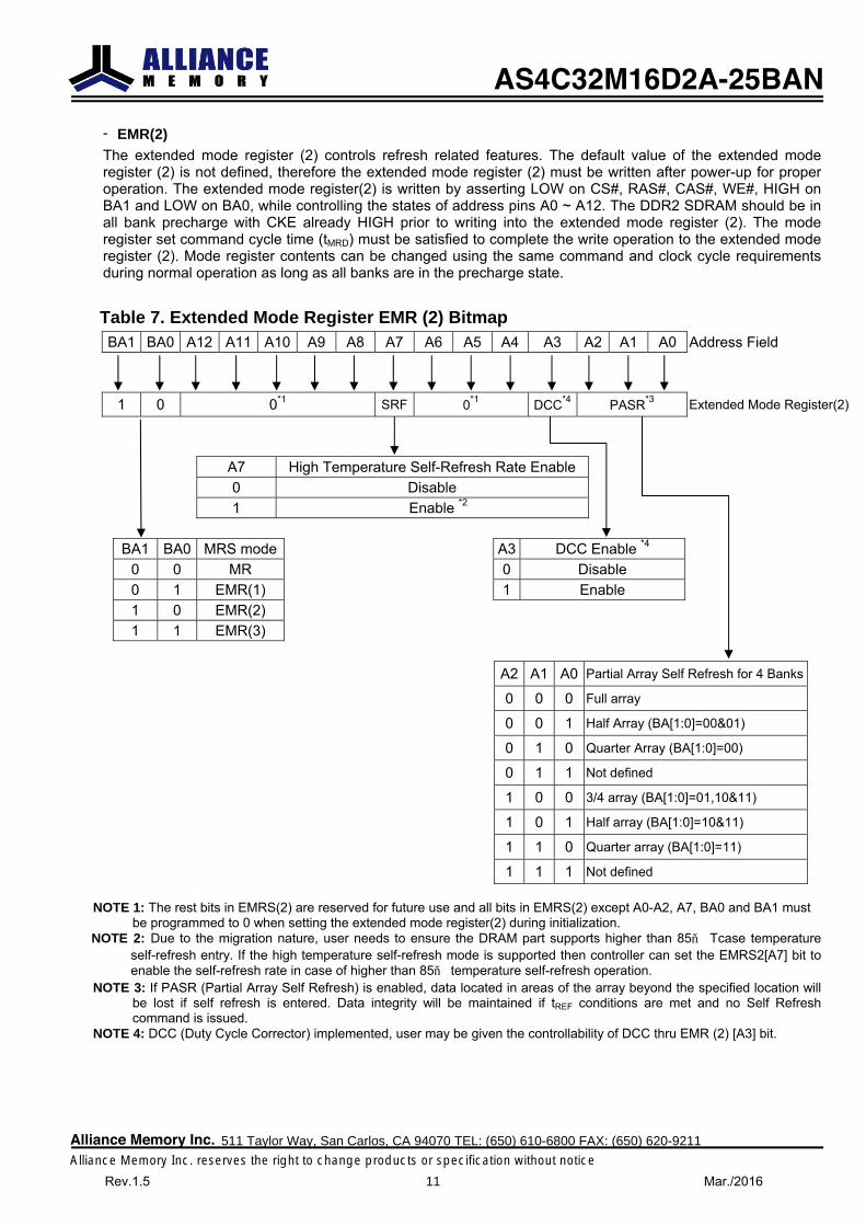
- EMR(2) The extended mode register (2) controls refresh related features. The default value of the extended mode register (2) is not defined, therefore the extended mode register (2) must be written after power-up for proper operation. The extended mode register(2) is written by asserting LOW on CS#, RAS#, CAS#, WE#, HIGH on BA1 and LOW on BA0, while controlling the states of address pins A0 ~ A12. The DDR2 SDRAM should be in all bank precharge with CKE already HIGH prior to writing into the extended mode register (2). The mode register set command cycle time (tMRD) must be satisfied to complete the write operation to the extended mode register (2). Mode register contents can be changed using the same command and clock cycle requirements during normal operation as long as all banks are in the precharge state.
Table 7. Extended Mode Register EMR (2) Bitmap BA1 BA0 A12 A11 A10 A9 A8 A7 A6 A5 A4 A3 A2 A1 A0 Address Field
1 0 0*1 SRF 0*1 DCC*4 PASR*3 Extended Mode Register(2)
A7 High Temperature Self-Refresh Rate Enable0 Disable 1 Enable *2
BA1 BA0 MRS mode A3 DCC Enable *4
0 0 MR 0 Disable 0 1 EMR(1) 1 Enable1 0 EMR(2) 1 1 EMR(3)
A2 A1 A0 Partial Array Self Refresh for 4 Banks
0 0 0 Full array
0 0 1 Half Array (BA[1:0]=00&01)
0 1 0 Quarter Array (BA[1:0]=00)
0 1 1 Not defined
1 0 0 3/4 array (BA[1:0]=01,10&11)
1 0 1 Half array (BA[1:0]=10&11)
1 1 0 Quarter array (BA[1:0]=11)
1 1 1 Not defined
NOTE 1: The rest bits in EMRS(2) are reserved for future use and all bits in EMRS(2) except A0-A2, A7, BA0 and BA1 must be programmed to 0 when setting the extended mode register(2) during initialization.
NOTE 2: Due to the migration nature, user needs to ensure the DRAM part supports higher than 85 Tcase temperature self-refresh entry. If the high temperature self-refresh mode is supported then controller can set the EMRS2[A7] bit to enable the self-refresh rate in case of higher than 85 temperature self-refresh operation.
NOTE 3: If PASR (Partial Array Self Refresh) is enabled, data located in areas of the array beyond the specified location will be lost if self refresh is entered. Data integrity will be maintained if tREF conditions are met and no Self Refresh command is issued.
NOTE 4: DCC (Duty Cycle Corrector) implemented, user may be given the controllability of DCC thru EMR (2) [A3] bit.
AS4C32M16D2A-25BAN
Alliance Memory Inc. 511 Taylor Way, San Carlos, CA 94070 TEL: (650) 610-6800 FAX: (650) 620-9211
Alliance Memory Inc. reserves the right to change products or specification without noticeRev.1.5 11 Mar./2016
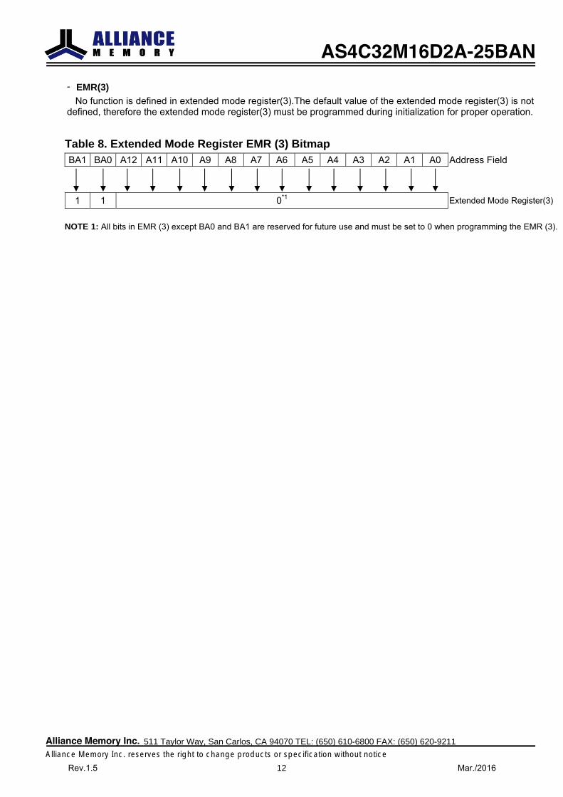
- EMR(3) No function is defined in extended mode register(3).The default value of the extended mode register(3) is not
defined, therefore the extended mode register(3) must be programmed during initialization for proper operation.
Table 8. Extended Mode Register EMR (3) Bitmap BA1 BA0 A12 A11 A10 A9 A8 A7 A6 A5 A4 A3 A2 A1 A0 Address Field
1 1 0*1 Extended Mode Register(3)
NOTE 1: All bits in EMR (3) except BA0 and BA1 are reserved for future use and must be set to 0 when programming the EMR (3).
AS4C32M16D2A-25BAN
Alliance Memory Inc. 511 Taylor Way, San Carlos, CA 94070 TEL: (650) 610-6800 FAX: (650) 620-9211
Alliance Memory Inc. reserves the right to change products or specification without noticeRev.1.5 12 Mar./2016
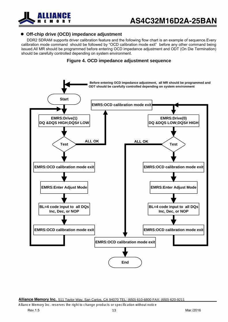
Off-chip drive (OCD) impedance adjustment DDR2 SDRAM supports driver calibration feature and the following flow chart is an example of sequence.Every
calibration mode command should be followed by “OCD calibration mode exit” before any other command being issued.All MR should be programmed before entering OCD impedance adjustment and ODT (On Die Termination) should be carefully controlled depending on system environment.
Figure 4. OCD impedance adjustment sequence
Start
EMRS:OCD calibration mode exit
EMRS:Drive(1)DQ &DQS HIGH;DQS# LOW
Test
EMRS:OCD calibration mode exit
EMRS:Enter Adjust Mode
BL=4 code input to all DQs Inc, Dec, or NOP
EMRS:OCD calibration mode exit
EMRS:Drive(0)DQ &DQS LOW;DQS# HIGH
Test
EMRS:OCD calibration mode exit
EMRS:Enter Adjust Mode
BL=4 code input to all DQs Inc, Dec, or NOP
EMRS:OCD calibration mode exit
End
EMRS:OCD calibration mode exit
ALL OK
Before entering OCD impedance adjustment, all MR should be programmed and ODT should be carefully controlled depending on system environment
ALL OK
AS4C32M16D2A-25BAN
Alliance Memory Inc. 511 Taylor Way, San Carlos, CA 94070 TEL: (650) 610-6800 FAX: (650) 620-9211
Alliance Memory Inc. reserves the right to change products or specification without noticeRev.1.5 13 Mar./2016
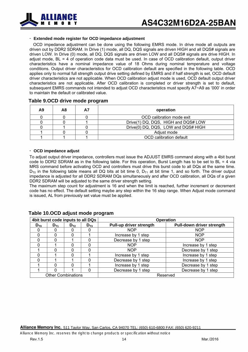
- Extended mode register for OCD impedance adjustment OCD impedance adjustment can be done using the following EMRS mode. In drive mode all outputs are
driven out by DDR2 SDRAM. In Drive (1) mode, all DQ, DQS signals are driven HIGH and all DQS# signals are driven LOW. In Drive (0) mode, all DQ, DQS signals are driven LOW and all DQS# signals are drive HIGH. In adjust mode, BL = 4 of operation code data must be used. In case of OCD calibration default, output driver characteristics have a nominal impedance value of 18 Ohms during nominal temperature and voltage conditions. Output driver characteristics for OCD calibration default are specified in the following table. OCD applies only to normal full strength output drive setting defined by EMRS and if half strength is set, OCD default driver characteristics are not applicable. When OCD calibration adjust mode is used, OCD default output driver characteristics are not applicable. After OCD calibration is completed or driver strength is set to default, subsequent EMRS commands not intended to adjust OCD characteristics must specify A7~A9 as ’000’ in order to maintain the default or calibrated value.
Table 9.OCD drive mode program
A9 A8 A7 operation
0 0 0 OCD calibration mode exit 0 0 1 Drive(1) DQ, DQS, HIGH and DQS# LOW 0 1 0 Drive(0) DQ, DQS, LOW and DQS# HIGH 1 0 0 Adjust mode1 1 1 OCD calibration default
- OCD impedance adjust To adjust output driver impedance, controllers must issue the ADJUST EMRS command along with a 4bit burst code to DDR2 SDRAM as in the following table. For this operation, Burst Length has to be set to BL = 4 via MRS command before activating OCD and controllers must drive this burst code to all DQs at the same time. DT0 in the following table means all DQ bits at bit time 0, DT1 at bit time 1, and so forth. The driver output impedance is adjusted for all DDR2 SDRAM DQs simultaneously and after OCD calibration, all DQs of a given DDR2 SDRAM will be adjusted to the same driver strength setting. The maximum step count for adjustment is 16 and when the limit is reached, further increment or decrement code has no effect. The default setting maybe any step within the 16 step range. When Adjust mode command is issued, AL from previously set value must be applied.
Table 10.OCD adjust mode program 4bit burst code inputs to all DQs Operation
DT0 DT1 DT2 DT3 Pull-up driver strength Pull-down driver strength 0 0 0 0 NOP NOP0 0 0 1 Increase by 1 step NOP0 0 1 0 Decrease by 1 step NOP0 1 0 0 NOP Increase by 1 step 1 0 0 0 NOP Decrease by 1 step 0 1 0 1 Increase by 1 step Increase by 1 step0 1 1 0 Decrease by 1 step Increase by 1 step1 0 0 1 Increase by 1 step Decrease by 1 step1 0 1 0 Decrease by 1 step Decrease by 1 step
Other Combinations Reserved
AS4C32M16D2A-25BAN
Alliance Memory Inc. 511 Taylor Way, San Carlos, CA 94070 TEL: (650) 610-6800 FAX: (650) 620-9211
Alliance Memory Inc. reserves the right to change products or specification without noticeRev.1.5 14 Mar./2016
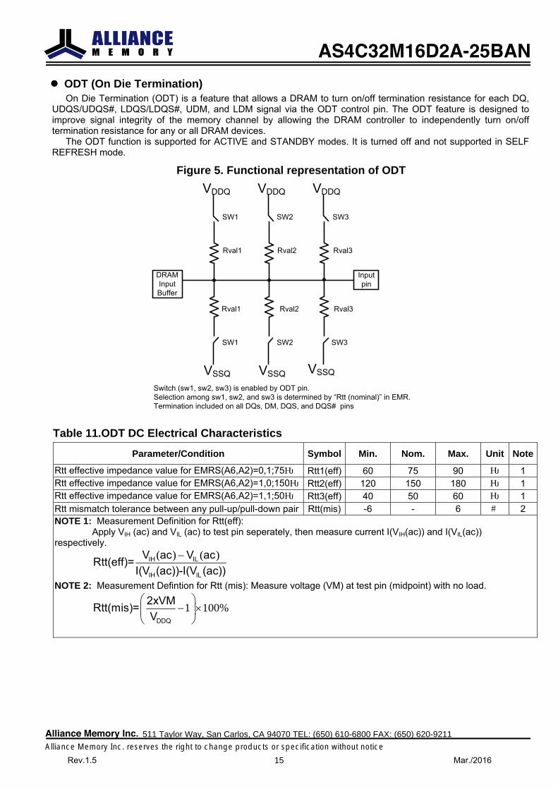
ODT (On Die Termination) On Die Termination (ODT) is a feature that allows a DRAM to turn on/off termination resistance for each DQ,
UDQS/UDQS#, LDQS/LDQS#, UDM, and LDM signal via the ODT control pin. The ODT feature is designed to improve signal integrity of the memory channel by allowing the DRAM controller to independently turn on/off termination resistance for any or all DRAM devices.
The ODT function is supported for ACTIVE and STANDBY modes. It is turned off and not supported in SELF REFRESH mode.
Figure 5. Functional representation of ODT
SW1
Rval1
VDDQ
SW1
Rval1
VSSQ
SW3
Rval3
VDDQ
SW3
Rval3
VSSQ
SW2
Rval2
VDDQ
SW2
Rval2
VSSQ
Input pin
DRAMInput Buffer
Switch (sw1, sw2, sw3) is enabled by ODT pin.Selection among sw1, sw2, and sw3 is determined by “Rtt (nominal)” in EMR. Termination included on all DQs, DM, DQS, and DQS# pins
Table 11.ODT DC Electrical Characteristics
Parameter/Condition Symbol Min. Nom. Max. Unit Note
Rtt effective impedance value for EMRS(A6,A2)=0,1;75Ω Rtt1(eff) 60 75 90 Ω 1 Rtt effective impedance value for EMRS(A6,A2)=1,0;150Ω Rtt2(eff) 120 150 180 Ω 1 Rtt effective impedance value for EMRS(A6,A2)=1,1;50Ω Rtt3(eff) 40 50 60 Ω 1 Rtt mismatch tolerance between any pull-up/pull-down pair Rtt(mis) -6 - 6 % 2 NOTE 1: Measurement Definition for Rtt(eff):
Apply VIH (ac) and VIL (ac) to test pin seperately, then measure current I(VIH(ac)) and I(VIL(ac)) respectively.
( ) ( )−IH IL
IH IL
V ac V acRtt(eff)=I(V (ac))-I(V (ac))
NOTE 2: Measurement Defintion for Rtt (mis): Measure voltage (VM) at test pin (midpoint) with no load.
1 100%⎛ ⎞
− ×⎜ ⎟⎝ ⎠DDQ
2xVMRtt(mis)=V
AS4C32M16D2A-25BAN
Alliance Memory Inc. 511 Taylor Way, San Carlos, CA 94070 TEL: (650) 610-6800 FAX: (650) 620-9211
Alliance Memory Inc. reserves the right to change products or specification without noticeRev.1.5 15 Mar./2016
Bank activate command The Bank Activate command is issued by holding CAS# and WE# HIGH with CS# and RAS# LOW at the rising edge of the clock. The bank addresses BA0 and BA1 are used to select the desired bank. The row addresses A0 through A12 are used to determine which row to activate in the selected bank. The Bank Activate command must be applied before any Read or Write operation can be executed. Immediately after the bank active command, the DDR2 SDRAM can accept a read or write command (with or without Auto-Precharge) on the following clock cycle. If a R/W command is issued to a bank that has not satisfied the tRCDmin specification, then additive latency must be programmed into the device to delay the R/W command which is internally issued to the device. The additive latency value must be chosen to assure tRCDmin is satisfied. Additive latencies of 0, 1, 2, 3, 4, and 5 are supported. Once a bank has been activated it must be precharged before another Bank Activate command can be applied to the same bank. The bank active and precharge times are defined as tRAS and tRP, respectively. The minimum time interval between successive Bank Activate commands to the same bank is determined (tRC). The minimum time interval between Bank Active commands is tRRD
Read and Write access modes After a bank has been activated, a Read or Write cycle can be executed. This is accomplished by setting RAS# HIGH, CS# and CAS# LOW at the clock’s rising edge. WE# must also be defined at this time to determine whether the access cycle is a Read operation (WE# HIGH) or a Write operation (WE# LOW). The DDR2 SDRAM provides a fast column access operation. A single Read or Write Command will initiate a serial Read or Write operation on successive clock cycles. The boundary of the burst cycle is strictly restricted to specific segments of the page length. Any system or application incorporating random access memory products should be properly designed, tested, and qualified to ensure proper use or access of such memory products. Disproportionate, excessive, and/or repeated access to a particular address or addresses may result in reduction of product life.
Posted CAS# Posted CAS# operation is supported to make command and data bus efficient for sustainable bandwidths in DDR2 SDRAM. In this operation, the DDR2 SDRAM allows a CAS# Read or Write command to be issued immediately after the RAS bank activate command (or any time during the RAS# -CAS#-delay time, tRCD, period). The command is held for the time of the Additive Latency (AL) before it is issued inside the device. The Read Latency (RL) is controlled by the sum of AL and the CAS latency (CL). Therefore if a user chooses to issue a R/W command before the tRCDmin, then AL (greater than 0) must be written into the EMR(1). The Write Latency (WL) is always defined as RL - 1 (Read Latency -1) where Read Latency is defined as the sum of additive latency plus CAS latency (RL=AL+CL). Read or Write operations using AL allow seamless bursts (refer to seamless operation timing diagram examples in Read burst and Write burst section)
Burst Mode Operation Burst mode operation is used to provide a constant flow of data to memory locations (Write cycle), or from memory locations (Read cycle). The parameters that define how the burst mode will operate are burst sequence and burst length. The DDR2 SDRAM supports 4 bit and 8 bit burst modes only. For 8 bit burst mode, full interleave address ordering is supported, however, sequential address ordering is nibble based for ease of implementation. The burst length is programmable and defined by the addresses A0 ~ A2 of the MRS. The burst type, either sequential or interleaved, is programmable and defined by the address bit 3 (A3) of the MRS. Seamless burst Read or Write operations are supported. Interruption of a burst Read or Write operation is prohibited, when burst length = 4 is programmed. For burst interruption of a Read or Write burst when burst length = 8 is used, see the “Burst Interruption“ section of this datasheet. A Burst Stop command is not supported on DDR2 SDRAM devices.
AS4C32M16D2A-25BAN
Alliance Memory Inc. 511 Taylor Way, San Carlos, CA 94070 TEL: (650) 610-6800 FAX: (650) 620-9211
Alliance Memory Inc. reserves the right to change products or specification without noticeRev.1.5 16 Mar./2016
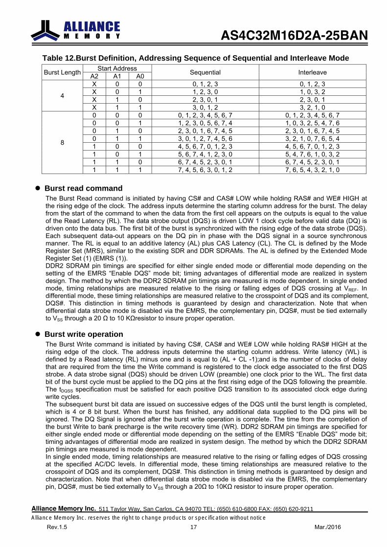
Table 12.Burst Definition, Addressing Sequence of Sequential and Interleave Mode
Burst Length Start Address Sequential InterleaveA2 A1 A0
4
X 0 0 0, 1, 2, 3 0, 1, 2, 3 X 0 1 1, 2, 3, 0 1, 0, 3, 2 X 1 0 2, 3, 0, 1 2, 3, 0, 1 X 1 1 3, 0, 1, 2 3, 2, 1, 0
8
0 0 0 0, 1, 2, 3, 4, 5, 6, 7 0, 1, 2, 3, 4, 5, 6, 7 0 0 1 1, 2, 3, 0, 5, 6, 7, 4 1, 0, 3, 2, 5, 4, 7, 6 0 1 0 2, 3, 0, 1, 6, 7, 4, 5 2, 3, 0, 1, 6, 7, 4, 5 0 1 1 3, 0, 1, 2, 7, 4, 5, 6 3, 2, 1, 0, 7, 6, 5, 4 1 0 0 4, 5, 6, 7, 0, 1, 2, 3 4, 5, 6, 7, 0, 1, 2, 3 1 0 1 5, 6, 7, 4, 1, 2, 3, 0 5, 4, 7, 6, 1, 0, 3, 2 1 1 0 6, 7, 4, 5, 2, 3, 0, 1 6, 7, 4, 5, 2, 3, 0, 1 1 1 1 7, 4, 5, 6, 3, 0, 1, 2 7, 6, 5, 4, 3, 2, 1, 0
Burst read command The Burst Read command is initiated by having CS# and CAS# LOW while holding RAS# and WE# HIGH at the rising edge of the clock. The address inputs determine the starting column address for the burst. The delay from the start of the command to when the data from the first cell appears on the outputs is equal to the value of the Read Latency (RL). The data strobe output (DQS) is driven LOW 1 clock cycle before valid data (DQ) is driven onto the data bus. The first bit of the burst is synchronized with the rising edge of the data strobe (DQS). Each subsequent data-out appears on the DQ pin in phase with the DQS signal in a source synchronous manner. The RL is equal to an additive latency (AL) plus CAS Latency (CL). The CL is defined by the Mode Register Set (MRS), similar to the existing SDR and DDR SDRAMs. The AL is defined by the Extended Mode Register Set (1) (EMRS (1)). DDR2 SDRAM pin timings are specified for either single ended mode or differential mode depending on the setting of the EMRS “Enable DQS” mode bit; timing advantages of differential mode are realized in system design. The method by which the DDR2 SDRAM pin timings are measured is mode dependent. In single ended mode, timing relationships are measured relative to the rising or falling edges of DQS crossing at VREF. In differential mode, these timing relationships are measured relative to the crosspoint of DQS and its complement, DQS#. This distinction in timing methods is guaranteed by design and characterization. Note that when differential data strobe mode is disabled via the EMRS, the complementary pin, DQS#, must be tied externally to VSS through a 20 Ω to 10 KΩresistor to insure proper operation.
Burst write operation The Burst Write command is initiated by having CS#, CAS# and WE# LOW while holding RAS# HIGH at the rising edge of the clock. The address inputs determine the starting column address. Write latency (WL) is defined by a Read latency (RL) minus one and is equal to (AL + CL -1);and is the number of clocks of delay that are required from the time the Write command is registered to the clock edge associated to the first DQS strobe. A data strobe signal (DQS) should be driven LOW (preamble) one clock prior to the WL. The first data bit of the burst cycle must be applied to the DQ pins at the first rising edge of the DQS following the preamble. The tDQSS specification must be satisfied for each positive DQS transition to its associated clock edge during write cycles. The subsequent burst bit data are issued on successive edges of the DQS until the burst length is completed, which is 4 or 8 bit burst. When the burst has finished, any additional data supplied to the DQ pins will be ignored. The DQ Signal is ignored after the burst write operation is complete. The time from the completion of the burst Write to bank precharge is the write recovery time (WR). DDR2 SDRAM pin timings are specified for either single ended mode or differential mode depending on the setting of the EMRS “Enable DQS” mode bit; timing advantages of differential mode are realized in system design. The method by which the DDR2 SDRAM pin timings are measured is mode dependent. In single ended mode, timing relationships are measured relative to the rising or falling edges of DQS crossing at the specified AC/DC levels. In differential mode, these timing relationships are measured relative to the crosspoint of DQS and its complement, DQS#. This distinction in timing methods is guaranteed by design and characterization. Note that when differential data strobe mode is disabled via the EMRS, the complementary pin, DQS#, must be tied externally to VSS through a 20Ω to 10KΩ resistor to insure proper operation.
AS4C32M16D2A-25BAN
Alliance Memory Inc. 511 Taylor Way, San Carlos, CA 94070 TEL: (650) 610-6800 FAX: (650) 620-9211
Alliance Memory Inc. reserves the right to change products or specification without noticeRev.1.5 17 Mar./2016
Write data mask One Write data mask (DM) pin for each 8 data bits (DQ) will be supported on DDR2 SDRAMs, Consistent with the implementation on DDR SDRAMs. It has identical timings on Write operations as the data bits, and though used in a uni-directional manner, is internally loaded identically to data bits to insure matched system timing. DM is not used during read cycles.
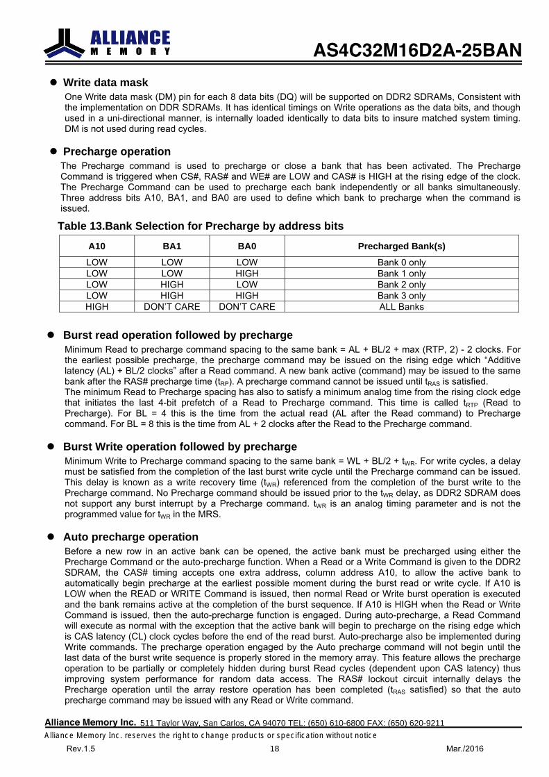
Precharge operation The Precharge command is used to precharge or close a bank that has been activated. The Precharge Command is triggered when CS#, RAS# and WE# are LOW and CAS# is HIGH at the rising edge of the clock. The Precharge Command can be used to precharge each bank independently or all banks simultaneously. Three address bits A10, BA1, and BA0 are used to define which bank to precharge when the command is issued.
Table 13.Bank Selection for Precharge by address bits
A10 BA1 BA0 Precharged Bank(s)
LOW LOW LOW Bank 0 only LOW LOW HIGH Bank 1 onlyLOW HIGH LOW Bank 2 onlyLOW HIGH HIGH Bank 3 onlyHIGH DON’T CARE DON’T CARE ALL Banks
Burst read operation followed by precharge Minimum Read to precharge command spacing to the same bank = AL + BL/2 + max (RTP, 2) - 2 clocks. For the earliest possible precharge, the precharge command may be issued on the rising edge which “Additive latency (AL) + BL/2 clocks” after a Read command. A new bank active (command) may be issued to the same bank after the RAS# precharge time (tRP). A precharge command cannot be issued until tRAS is satisfied. The minimum Read to Precharge spacing has also to satisfy a minimum analog time from the rising clock edge that initiates the last 4-bit prefetch of a Read to Precharge command. This time is called tRTP (Read to Precharge). For BL = 4 this is the time from the actual read (AL after the Read command) to Precharge command. For BL = 8 this is the time from AL + 2 clocks after the Read to the Precharge command.
Burst Write operation followed by precharge Minimum Write to Precharge command spacing to the same bank = WL + BL/2 + tWR. For write cycles, a delay must be satisfied from the completion of the last burst write cycle until the Precharge command can be issued. This delay is known as a write recovery time (tWR) referenced from the completion of the burst write to the Precharge command. No Precharge command should be issued prior to the tWR delay, as DDR2 SDRAM does not support any burst interrupt by a Precharge command. tWR is an analog timing parameter and is not the programmed value for tWR in the MRS.
Auto precharge operation Before a new row in an active bank can be opened, the active bank must be precharged using either the Precharge Command or the auto-precharge function. When a Read or a Write Command is given to the DDR2 SDRAM, the CAS# timing accepts one extra address, column address A10, to allow the active bank to automatically begin precharge at the earliest possible moment during the burst read or write cycle. If A10 is LOW when the READ or WRITE Command is issued, then normal Read or Write burst operation is executed and the bank remains active at the completion of the burst sequence. If A10 is HIGH when the Read or Write Command is issued, then the auto-precharge function is engaged. During auto-precharge, a Read Command will execute as normal with the exception that the active bank will begin to precharge on the rising edge which is CAS latency (CL) clock cycles before the end of the read burst. Auto-precharge also be implemented during Write commands. The precharge operation engaged by the Auto precharge command will not begin until the last data of the burst write sequence is properly stored in the memory array. This feature allows the precharge operation to be partially or completely hidden during burst Read cycles (dependent upon CAS latency) thus improving system performance for random data access. The RAS# lockout circuit internally delays the Precharge operation until the array restore operation has been completed (tRAS satisfied) so that the auto precharge command may be issued with any Read or Write command.
AS4C32M16D2A-25BAN
Alliance Memory Inc. 511 Taylor Way, San Carlos, CA 94070 TEL: (650) 610-6800 FAX: (650) 620-9211
Alliance Memory Inc. reserves the right to change products or specification without noticeRev.1.5 18 Mar./2016
Burst read with auto precharge If A10 is HIGH when a Read Command is issued, the Read with Auto-Precharge function is engaged. The DDR2 SDRAM starts an Auto-Precharge operation on the rising edge which is (AL + BL/2) cycles later from the Read with AP command if tRAS(min) and tRTP are satisfied. If tRAS(min) is not satisfied at the edge, the start point of Auto-Precharge operation will be delayed until tRAS(min) is satisfied. If tRTP(min) is not satisfied at the edge, the start point of Auto-precharge operation will be delayed until tRTP(min) is satisfied. In case the internal precharge is pushed out by tRTP, tRP starts at the point where the internal precharge happens (not at the next rising clock edge after this event). So for BL = 4 the minimum time from Read with Auto-Precharge to the next Activate command becomes AL + tRTP + tRP. For BL = 8 the time from Read with Auto-Precharge to the next Activate command is AL + 2 + tRTP + tRP. Note that both parameters tRTP and tRP have to be rounded up to the next integer value. In any event internal precharge does not start earlier than two clocks after the last 4-bit prefetch. A new bank active (command) may be issued to the same bank if the following two conditions are satisfied simultaneously: (1) The RAS# precharge time (tRP) has been satisfied from the clock at which the Auto-Precharge begins. (2) The RAS# cycle time (tRC) from the previous bank activation has been satisfied.
Burst write with auto precharge If A10 is HIGH when a Write Command is issued, the Write with Auto-Precharge function is engaged. The DDR2 SDRAM automatically begins precharge operation after the completion of the burst write plus Write recovery time (tWR). The bank undergoing auto-precharge from the completion of the write burst may be reactivated if the following two conditions are satisfied. (1) The data-in to bank activate delay time (WR + tRP) has been satisfied. (2) The RAS# cycle time (tRC) from the previous bank activation has been satisfied.
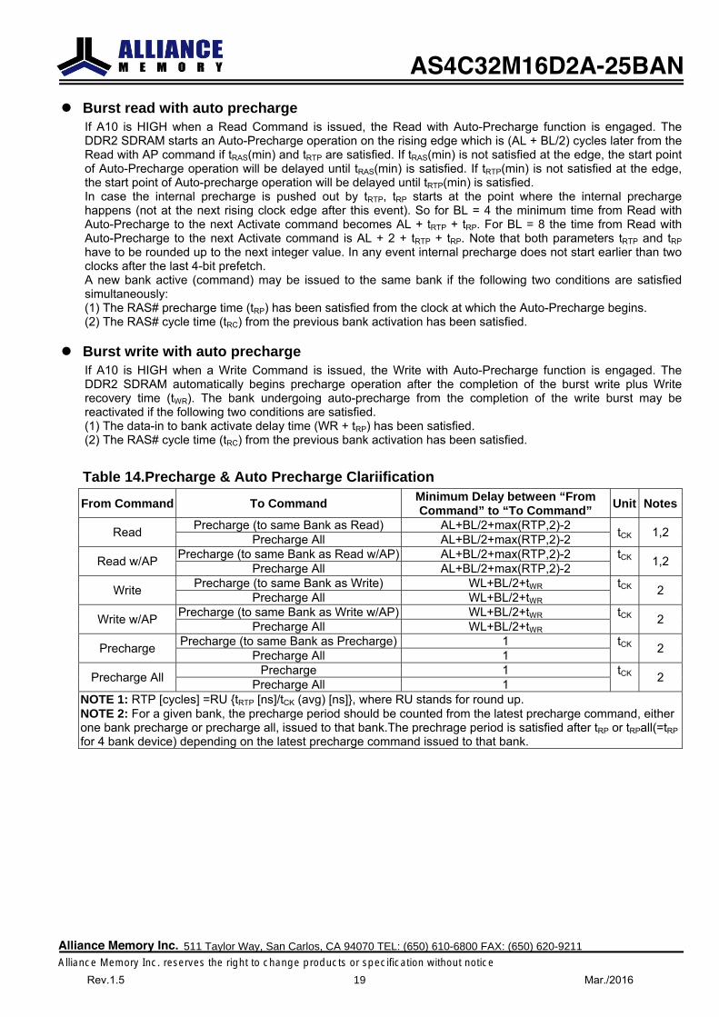
Table 14.Precharge & Auto Precharge Clariification
From Command To Command Minimum Delay between “From Command” to “To Command” Unit Notes
Read Precharge (to same Bank as Read) AL+BL/2+max(RTP,2)-2 tCK 1,2 Precharge All AL+BL/2+max(RTP,2)-2
Read w/AP Precharge (to same Bank as Read w/AP) AL+BL/2+max(RTP,2)-2 tCK 1,2Precharge All AL+BL/2+max(RTP,2)-2
Write Precharge (to same Bank as Write) WL+BL/2+tWR tCK 2 Precharge All WL+BL/2+tWR
Write w/AP Precharge (to same Bank as Write w/AP) WL+BL/2+tWR tCK 2 Precharge All WL+BL/2+tWR
Precharge Precharge (to same Bank as Precharge) 1 tCK 2 Precharge All 1
Precharge All Precharge 1 tCK 2 Precharge All 1NOTE 1: RTP [cycles] =RU tRTP [ns]/tCK (avg) [ns], where RU stands for round up. NOTE 2: For a given bank, the precharge period should be counted from the latest precharge command, either one bank precharge or precharge all, issued to that bank.The prechrage period is satisfied after tRP or tRPall(=tRP for 4 bank device) depending on the latest precharge command issued to that bank.
AS4C32M16D2A-25BAN
Alliance Memory Inc. 511 Taylor Way, San Carlos, CA 94070 TEL: (650) 610-6800 FAX: (650) 620-9211
Alliance Memory Inc. reserves the right to change products or specification without noticeRev.1.5 19 Mar./2016
Refresh command When CS#, RAS# and CAS# are held LOW and WE# HIGH at the rising edge of the clock, the chip enters the Refresh mode (REF). All banks of the DDR2 SDRAM must be precharged and idle for a minimum of the Precharge time (tRP) before the Refresh command (REF) can be applied. An address counter, internal to the device, supplies the bank address during the refresh cycle. No control of the external address bus is required once this cycle has started. When the refresh cycle has completed, all banks of the DDR2 SDRAM will be in the precharged (idle) state. A delay between the Refresh command (REF) and the next Activate command or subsequent Refresh command must be greater than or equal to the Refresh cycle time (tRFC).To allow for improved efficiency in scheduling and switching between tasks, some flexibility in the absolute refresh interval is provided. A maximum of eight Refresh commands can be posted to any given DDR2 SDRAM, meaning that the maximum absolute interval between any Refresh command and the next Refresh command is 9 * tREFI.
Self refresh operation The Self Refresh command can be used to retain data in the DDR2 SDRAM, even if the rest of the system is powered down. When in the Self Refresh mode, the DDR2 SDRAM retains data without external clocking. The DDR2 SDRAM device has a built-in timer to accommodate Self Refresh operation. The Self Refresh Command is defined by having CS#, RAS#, CAS# and CKE# held LOW with WE# HIGH at the rising edge of the clock. ODT must be turned off before issuing Self Refresh command, by either driving ODT pin LOW or using EMRS command. Once the Command is registered, CKE must be held LOW to keep the device in Self Refresh mode. The DLL is automatically disabled upon entering Self Refresh and is automatically enabled upon exiting Self Refresh. When the DDR2 SDRAM has entered Self Refresh mode all of the external signals except CKE, are “don’t care”. For proper Self Refresh operation all power supply pins (VDD, VDDQ, VDDL and VREF) must be at valid levels. The DRAM initiates a minimum of one refresh command internally within tCKE period once it enters Self Refresh mode. The clock is internally disabled during Self Refresh Operation to save power. The minimum time that the DDR2 SDRAM must remain in Self Refresh mode is tCKE. The user may change the external clock frequency or halt the external clock one clock after Self Refresh entry is registered, however, the clock must be restarted and stable before the device can exit Self Refresh operation. The procedure for exiting Self Refresh requires a sequence of commands. First, the clock must be stable prior to CKE going back HIGH. Once Self Refresh Exit is registered, a delay of at least tXSNR must be satisfied before a valid command can be issued to the device to allow for any internal refresh in progress. CKE must remain HIGH for the entire Self Refresh exit period tXSRD for proper operation except for Self Refresh re-entry. Upon exit from Self Refresh, the DDR2 SDRAM can be put back into Self Refresh mode after waiting at least tXSNR period and issuing one refresh command(refresh period of tRFC). NOP or deselect commands must be registered on each positive clock edge during the Self Refresh exit interval tXSNR. ODT should be turned off during tXSRD. The use of Self Refresh mode introduces the possibility that an internally timed refresh event can be missed when CKE is raised for exit from Self Refresh mode. Upon exit from Self Refresh, the DDR2 SDRAM requires a minimum of one extra auto refresh command before it is put back into Self Refresh mode.
AS4C32M16D2A-25BAN
Alliance Memory Inc. 511 Taylor Way, San Carlos, CA 94070 TEL: (650) 610-6800 FAX: (650) 620-9211
Alliance Memory Inc. reserves the right to change products or specification without noticeRev.1.5 20 Mar./2016
Power-Down Power-down is synchronously entered when CKE is registered LOW along with NOP or Deselect command. No read or write operation may be in progress when CKE goes LOW. These operations are any of the following: read burst or write burst and recovery. CKE is allowed to go LOW while any of other operations such as row activation, precharge or autoprecharge, mode register or extended mode register command time, or autorefresh is in progress. The DLL should be in a locked state when power-down is entered. Otherwise DLL should be reset after exiting power-down mode for proper read operation. If power-down occurs when all banks are precharged, this mode is referred to as Precharge Power-down; if power-down occurs when there is a row active in any bank, this mode is referred to as Active Power-down. For Active Power-down two different power saving modes can be selected within the MRS register, address bit A12. When A12 is set to “LOW” this mode is referred as “standard active power-down mode” and a fast power-down exit timing defined by the tXARD timing parameter can be used. When A12 is set to “HIGH” this mode is referred as a power saving “LOW power active power-down mode”. This mode takes longer to exit from the power-down mode and the tXARDS timing parameter has to be satisfied. Entering power-down deactivates the input and output buffers, excluding CK, CK#, ODT and CKE. Also the DLL is disabled upon entering precharge power-down or slow exit active power-down, but the DLL is kept enabled during fast exit active power-down. In power-down mode, CKE LOW and a stable clock signal must be maintained at the inputs of the DDR2 SDRAM, and all other input signals are “Don’t Care”. Power-down duration is limited by 9 times tREFI of the device. The power-down state is synchronously exited when CKE is registered HIGH (along with a NOP or Deselect command). A valid, executable command can be applied with power-down exit latency, tXP, tXARD or tXARDS, after CKE goes HIGH. Power-down exit latencies are defined in the AC spec table of this data sheet.
Asynchronous CKE LOW Event DRAM requires CKE to be maintained “HIGH” for all valid operations as defined in this datasheet. If CKE asynchronously drops “LOW” during any valid peration DRAM is not guaranteed to preserve the contents of array. If this event occurs, memory controller must satisfy DRAM timing specification tDelay efore turning off the clocks. Stable clocks must exist at the input of DRAM before CKE is raised “HIGH” again. DRAM must be fully re-initialized. DRAM is ready for normal operation after the initialization sequence.
Input clock frequency change during precharge power down DDR2 SDRAM input clock frequency can be changed under following condition: DDR2 SDRAM is in precharged power down mode. ODT must be turned off and CKE must be at logic LOW level. A minimum of 2 clocks must be waited after CKE goes LOW before clock frequency may change. SDRAM input clock frequency is allowed to change only within minimum and maximum operating frequency specified for the particular speed grade. During input clock frequency change, ODT and CKE must be held at stable LOW levels. Once input clock frequency is changed, stable new clocks must be provided to DRAM before precharge power down may be exited and DLL must be RESET via EMRS after precharge power down exit. Depending on new clock frequency an additional MRS command may need to be issued to appropriately set the WR, CL etc. During DLL re-lock period, ODT must remain off. After the DLL lock time, the DRAM is ready to operate with new clock frequency.
No operation command The No Operation Command should be used in cases when the DDR2 SDRAM is in an idle or a wait state. The purpose of the No Operation Command (NOP) is to prevent the DDR2 SDRAM from registering any unwanted commands between operations. A No Operation Command is registered when CS# is LOW with RAS#, CAS#, and WE# held HIGH at the rising edge of the clock. A No Operation Command will not terminate a previous operation that is still executing, such as a burst read or write cycle.
Deselect command The Deselect Command performs the same function as a No Operation Command. Deselect Command occurs when CS# is brought HIGH at the rising edge of the clock, the RAS#, CAS#, and WE# signals become don’t cares.
AS4C32M16D2A-25BAN
Alliance Memory Inc. 511 Taylor Way, San Carlos, CA 94070 TEL: (650) 610-6800 FAX: (650) 620-9211
Alliance Memory Inc. reserves the right to change products or specification without noticeRev.1.5 21 Mar./2016
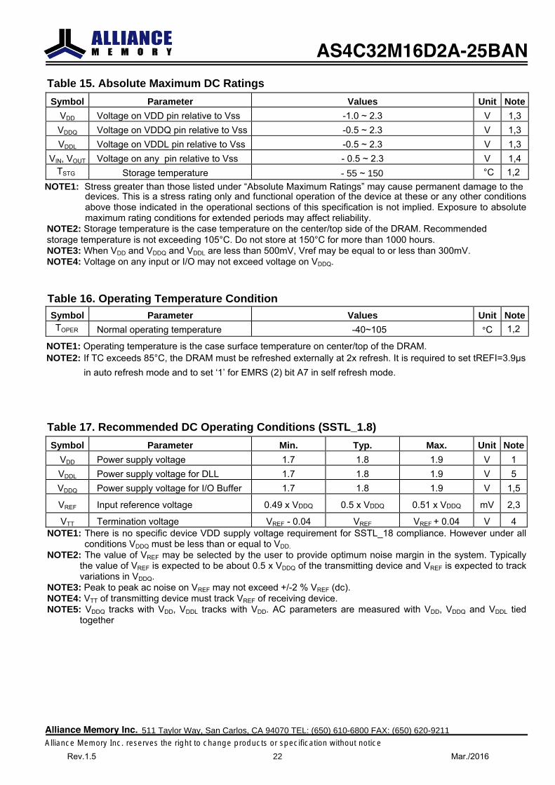
Table 15. Absolute Maximum DC Ratings Symbol Parameter Values Unit Note
VDD Voltage on VDD pin relative to Vss -1.0 ~ 2.3 V 1,3VDDQ Voltage on VDDQ pin relative to Vss -0.5 ~ 2.3 V 1,3VDDL Voltage on VDDL pin relative to Vss -0.5 ~ 2.3 V 1,3
VIN, VOUT Voltage on any pin relative to Vss - 0.5 ~ 2.3 V 1,4Storage temperatureTSTG
Table 16. Operating Temperature Condition
devices. This is a stress rating only and functional operation of the device at these or any other conditions above those indicated in the operational sections of this specification is not implied. Exposure to absolute maximum rating conditions for extended periods may affect reliability.
NOTE2: Storage temperature is the case temperature on the center/top side of the DRAM. Recommended storage temperature is not exceeding 105°C. Do not store at 150°C for more than 1000 hours. NOTE3: When VDD and VDDQ and VDDL are less than 500mV, Vref may be equal to or less than 300mV. NOTE4: Voltage on any input or I/O may not exceed voltage on VDDQ.
Symbol Parameter Values Unit NoteTOPER Normal operating temperature -40~105 °C
NOTE1: Operating temperature is the case surface temperature on center/top of the DRAM. NOTE2: If TC exceeds 85°C, the DRAM must be refreshed externally at 2x refresh. It is required to set tREFI=3.9µs
in auto refresh mode and to set ‘1’ for EMRS (2) bit A7 in self refresh mode.
Table 17. Recommended DC Operating Conditions (SSTL_1.8) Symbol Parameter Min. Typ. Max. Unit Note
VDD Power supply voltage 1.7 1.8 1.9 V 1 VDDL Power supply voltage for DLL 1.7 1.8 1.9 V 5 VDDQ Power supply voltage for I/O Buffer 1.7 1.8 1.9 V 1,5
VREF Input reference voltage 0.49 x VDDQ 0.5 x VDDQ 0.51 x VDDQ mV 2,3
VTT Termination voltage VREF - 0.04 VREF VREF + 0.04 V 4 NOTE1: There is no specific device VDD supply voltage requirement for SSTL_18 compliance. However under all
conditions VDDQ must be less than or equal to VDD. NOTE2: The value of VREF may be selected by the user to provide optimum noise margin in the system. Typically
the value of VREF is expected to be about 0.5 x VDDQ of the transmitting device and VREF is expected to track variations in VDDQ.
NOTE3: Peak to peak ac noise on VREF may not exceed +/-2 % VREF (dc). NOTE4: VTT of transmitting device must track VREF of receiving device. NOTE5: VDDQ tracks with VDD, VDDL tracks with VDD. AC parameters are measured with VDD, VDDQ and VDDL tied
together
AS4C32M16D2A-25BAN
Alliance Memory Inc. 511 Taylor Way, San Carlos, CA 94070 TEL: (650) 610-6800 FAX: (650) 620-9211
Alliance Memory Inc. reserves the right to change products or specification without noticeRev.1.5 22 Mar./2016
NOTE1: Stress greater than those listed under “Absolute Maximum Ratings” may cause permanent damage to the - 55 ~ 150 °C 1,2
1,2
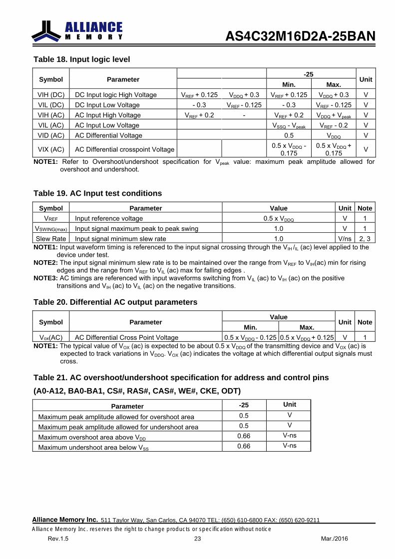
Table 18. Input logic level
Symbol Parameter-25
UnitMin. Max.
VIH (DC) DC Input logic High Voltage VREF + 0.125 VDDQ + 0.3 VREF + 0.125 VDDQ + 0.3 V VIL (DC) DC Input Low Voltage - 0.3 VREF - 0.125 - 0.3 VREF - 0.125 V VIH (AC) AC Input High Voltage VREF + 0.2 - VREF + 0.2 VDDQ + Vpeak V VIL (AC) AC Input Low Voltage VSSQ - Vpeak VREF - 0.2 V VID (AC) AC Differential Voltage 0.5 VDDQ V
VIX (AC) AC Differential crosspoint Voltage 0.5 x VDDQ - 0.175
0.5 x VDDQ + 0.175 V
NOTE1: Refer to Overshoot/undershoot specification for Vpeak value: maximum peak amplitude allowed for overshoot and undershoot.
Table 19. AC Input test conditions Symbol Parameter Value Unit Note
VREF Input reference voltage 0.5 x VDDQ V 1 VSWING(max) Input signal maximum peak to peak swing 1.0 V 1 Slew Rate Input signal minimum slew rate 1.0 V/ns 2, 3
NOTE1: Input waveform timing is referenced to the input signal crossing through the VIH /IL (ac) level applied to the device under test.
NOTE2: The input signal minimum slew rate is to be maintained over the range from VREF to VIH(ac) min for rising edges and the range from VREF to VIL (ac) max for falling edges .
NOTE3: AC timings are referenced with input waveforms switching from VIL (ac) to VIH (ac) on the positive transitions and VIH (ac) to VIL (ac) on the negative transitions.
Table 20. Differential AC output parameters
Symbol ParameterValue
Unit NoteMin. Max.
Vox(AC) AC Differential Cross Point Voltage 0.5 x VDDQ - 0.125 0.5 x VDDQ + 0.125 V 1 NOTE1: The typical value of VOX (ac) is expected to be about 0.5 x VDDQ of the transmitting device and VOX (ac) is
expected to track variations in VDDQ. VOX (ac) indicates the voltage at which differential output signals must cross.
Table 21. AC overshoot/undershoot specification for address and control pins (A0-A12, BA0-BA1, CS#, RAS#, CAS#, WE#, CKE, ODT)
Parameter -25 Unit
Maximum peak amplitude allowed for overshoot area 0.5 V
Maximum peak amplitude allowed for undershoot area 0.5 V
Maximum overshoot area above VDD 0.66 V-ns
Maximum undershoot area below VSS 0.66 V-ns
AS4C32M16D2A-25BAN
Alliance Memory Inc. 511 Taylor Way, San Carlos, CA 94070 TEL: (650) 610-6800 FAX: (650) 620-9211
Alliance Memory Inc. reserves the right to change products or specification without noticeRev.1.5 23 Mar./2016
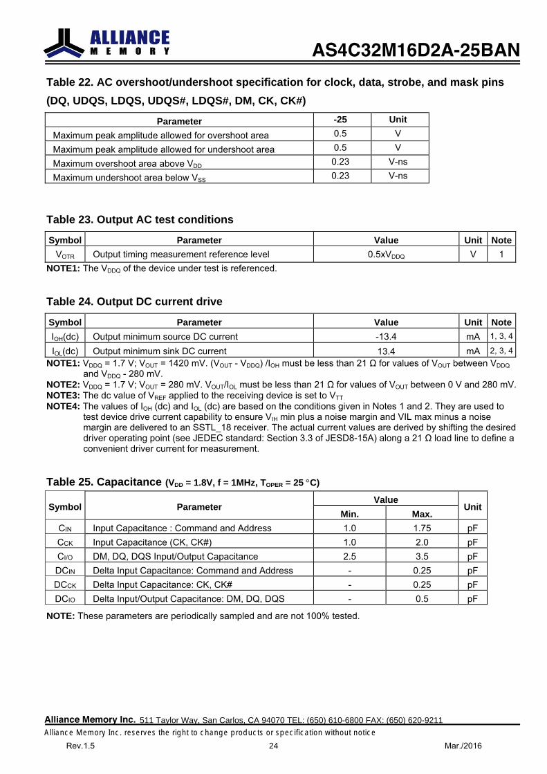
Table 22. AC overshoot/undershoot specification for clock, data, strobe, and mask pins (DQ, UDQS, LDQS, UDQS#, LDQS#, DM, CK, CK#)
Parameter -25 UnitMaximum peak amplitude allowed for overshoot area 0.5 V
Maximum peak amplitude allowed for undershoot area 0.5 V
Maximum overshoot area above VDD 0.23 V-ns
Maximum undershoot area below VSS 0.23 V-ns
Table 23. Output AC test conditions
Symbol Parameter Value Unit NoteVOTR Output timing measurement reference level 0.5xVDDQ V 1
NOTE1: The VDDQ of the device under test is referenced.
Table 24. Output DC current drive Symbol Parameter Value Unit NoteIOH(dc) Output minimum source DC current -13.4 mA 1, 3, 4
IOL(dc) Output minimum sink DC current 13.4 mA 2, 3, 4NOTE1: VDDQ = 1.7 V; VOUT = 1420 mV. (VOUT - VDDQ) /IOH must be less than 21 Ω for values of VOUT between VDDQ
and VDDQ - 280 mV. NOTE2: VDDQ = 1.7 V; VOUT = 280 mV. VOUT/IOL must be less than 21 Ω for values of VOUT between 0 V and 280 mV. NOTE3: The dc value of VREF applied to the receiving device is set to VTT NOTE4: The values of IOH (dc) and IOL (dc) are based on the conditions given in Notes 1 and 2. They are used to
test device drive current capability to ensure VIH min plus a noise margin and VIL max minus a noise margin are delivered to an SSTL_18 receiver. The actual current values are derived by shifting the desired driver operating point (see JEDEC standard: Section 3.3 of JESD8-15A) along a 21 Ω load line to define a convenient driver current for measurement.
Table 25. Capacitance (VDD = 1.8V, f = 1MHz, TOPER = 25 °C)
Symbol ParameterValue
UnitMin. Max.
CIN Input Capacitance : Command and Address 1.0 1.75 pF CCK Input Capacitance (CK, CK#) 1.0 2.0 pF CI/O DM, DQ, DQS Input/Output Capacitance 2.5 3.5 pF DCIN Delta Input Capacitance: Command and Address - 0.25 pF DCCK Delta Input Capacitance: CK, CK# - 0.25 pF DCIO Delta Input/Output Capacitance: DM, DQ, DQS - 0.5 pF
NOTE: These parameters are periodically sampled and are not 100% tested.
AS4C32M16D2A-25BAN
Alliance Memory Inc. 511 Taylor Way, San Carlos, CA 94070 TEL: (650) 610-6800 FAX: (650) 620-9211
Alliance Memory Inc. reserves the right to change products or specification without noticeRev.1.5 24 Mar./2016
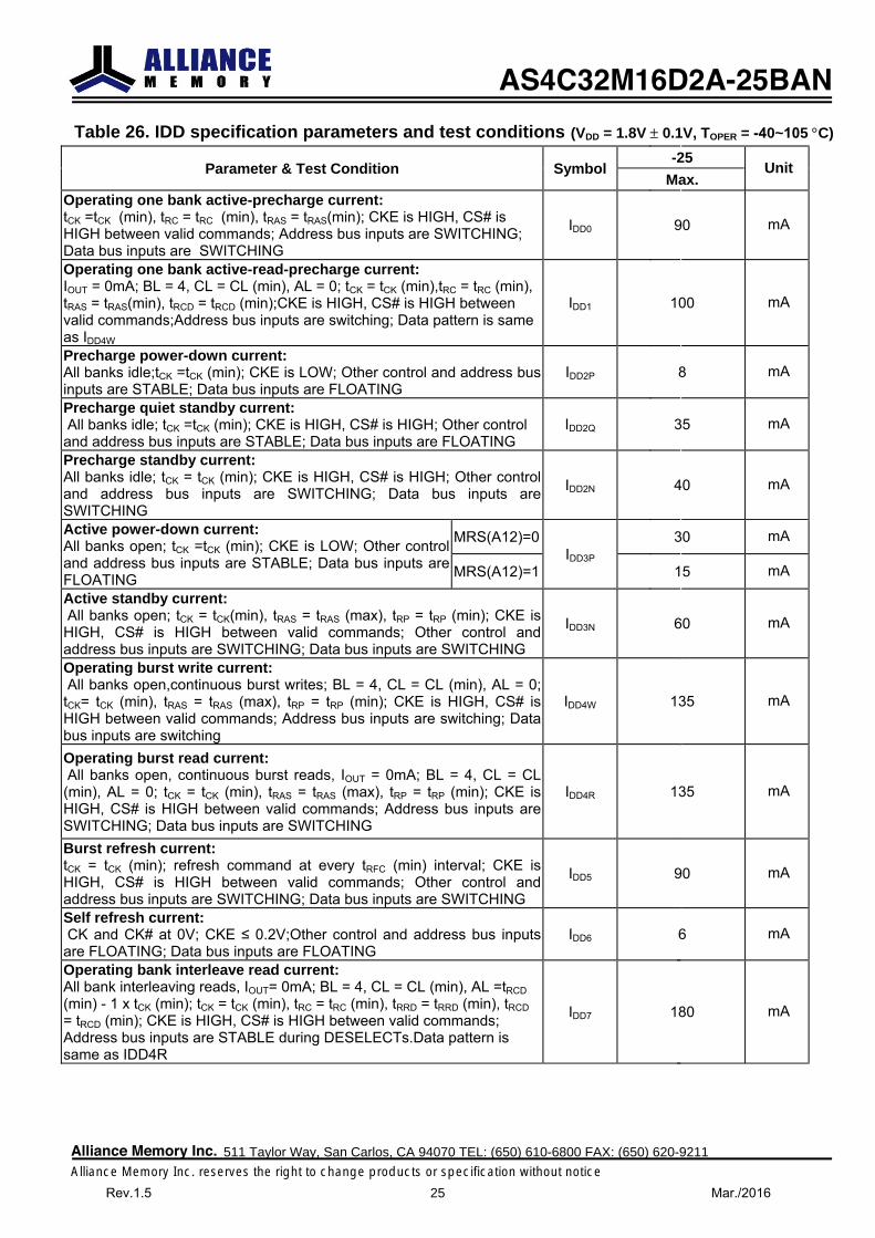
Table 26. IDD specification parameters and test conditions (VDD = 1.8V ± 0.1V, TOPER = -40~105 °C)
Parameter & Test Condition Symbol-25
UnitMax.
Operating one bank active-precharge current: tCK =tCK (min), tRC = tRC (min), tRAS = tRAS(min); CKE is HIGH, CS# is HIGH between valid commands; Address bus inputs are SWITCHING; Data bus inputs are SWITCHING
IDD0 90 mA
Operating one bank active-read-precharge current: IOUT = 0mA; BL = 4, CL = CL (min), AL = 0; tCK = tCK (min),tRC = tRC (min), tRAS = tRAS(min), tRCD = tRCD (min);CKE is HIGH, CS# is HIGH between valid commands;Address bus inputs are switching; Data pattern is same as IDD4W
IDD1 100 mA
Precharge power-down current: All banks idle;tCK =tCK (min); CKE is LOW; Other control and address businputs are STABLE; Data bus inputs are FLOATING
IDD2P 8 mA
Precharge quiet standby current: All banks idle; tCK =tCK (min); CKE is HIGH, CS# is HIGH; Other control and address bus inputs are STABLE; Data bus inputs are FLOATING
IDD2Q 35 mA
Precharge standby current: All banks idle; tCK = tCK (min); CKE is HIGH, CS# is HIGH; Other control and address bus inputs are SWITCHING; Data bus inputs areSWITCHING
IDD2N 40 mA
Active power-down current: All banks open; tCK =tCK (min); CKE is LOW; Other control and address bus inputs are STABLE; Data bus inputs are FLOATING
MRS(A12)=0IDD3P
30 mA
MRS(A12)=1 15 mA
Active standby current: All banks open; tCK = tCK(min), tRAS = tRAS (max), tRP = tRP (min); CKE is HIGH, CS# is HIGH between valid commands; Other control andaddress bus inputs are SWITCHING; Data bus inputs are SWITCHING
IDD3N 60 mA
Operating burst write current: All banks open,continuous burst writes; BL = 4, CL = CL (min), AL = 0; tCK= tCK (min), tRAS = tRAS (max), tRP = tRP (min); CKE is HIGH, CS# is HIGH between valid commands; Address bus inputs are switching; Data bus inputs are switching
IDD4W 135 mA
Operating burst read current: All banks open, continuous burst reads, IOUT = 0mA; BL = 4, CL = CL (min), AL = 0; tCK = tCK (min), tRAS = tRAS (max), tRP = tRP (min); CKE is HIGH, CS# is HIGH between valid commands; Address bus inputs are SWITCHING; Data bus inputs are SWITCHING
IDD4R 135 mA
Burst refresh current: tCK = tCK (min); refresh command at every tRFC (min) interval; CKE is HIGH, CS# is HIGH between valid commands; Other control andaddress bus inputs are SWITCHING; Data bus inputs are SWITCHING
IDD5 90 mA
Self refresh current: CK and CK# at 0V; CKE ≤ 0.2V;Other control and address bus inputs are FLOATING; Data bus inputs are FLOATING
IDD6 6 mA
Operating bank interleave read current: All bank interleaving reads, IOUT= 0mA; BL = 4, CL = CL (min), AL =tRCD (min) - 1 x tCK (min); tCK = tCK (min), tRC = tRC (min), tRRD = tRRD (min), tRCD = tRCD (min); CKE is HIGH, CS# is HIGH between valid commands; Address bus inputs are STABLE during DESELECTs.Data pattern is same as IDD4R
IDD7 180 mA
AS4C32M16D2A-25BAN
Alliance Memory Inc. 511 Taylor Way, San Carlos, CA 94070 TEL: (650) 610-6800 FAX: (650) 620-9211
Alliance Memory Inc. reserves the right to change products or specification without noticeRev.1.5 25 Mar./2016
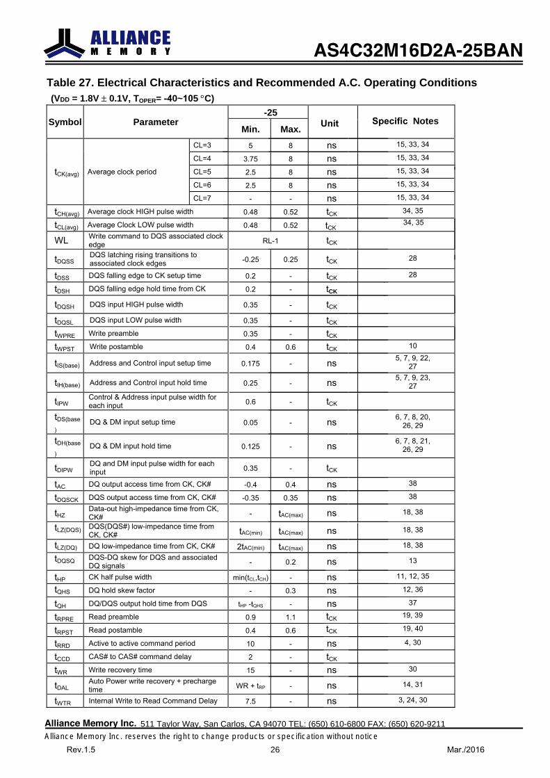
Table 27. Electrical Characteristics and Recommended A.C. Operating Conditions
Symbol Parameter-25
Unit Specific NotesMin. Max.
tCK(avg) Average clock period
CL=3 5 8 ns 15, 33, 34
CL=4 3.75 8 ns 15, 33, 34
CL=5 2.5 8 ns 15, 33, 34
CL=6 2.5 8 ns 15, 33, 34
CL=7 - - ns 15, 33, 34
tCH(avg) Average clock HIGH pulse width 0.48 0.52 tCK 34, 35
tCL(avg) Average Clock LOW pulse width 0.48 0.52 34, 35
WL Write command to DQS associated clock edge RL-1 tCK
tDQSS DQS latching rising transitions to associated clock edges -0.25 0.25 tCK 28
tDSS DQS falling edge to CK setup time 0.2 - tCK 28
tDSH DQS falling edge hold time from CK 0.2 - tCK
tDQSH DQS input HIGH pulse width 0.35 - tCK
tDQSL DQS input LOW pulse width 0.35 - tCK
tWPRE Write preamble 0.35 - tCK
tWPST Write postamble 0.4 0.6 tCK 10
tIS(base) Address and Control input setup time 0.175 - ns 5, 7, 9, 22, 27
tIH(base) Address and Control input hold time 0.25 - ns 5, 7, 9, 23, 27
tIPW Control & Address input pulse width for each input 0.6 - tCK
tDS(base
)DQ & DM input setup time 0.05 - ns 6, 7, 8, 20,
26, 29
tDH(base
)DQ & DM input hold time 0.125 - ns 6, 7, 8, 21,
26, 29
tDIPW DQ and DM input pulse width for each input 0.35 - tCK
tAC DQ output access time from CK, CK# -0.4 0.4 ns 38
tDQSCK DQS output access time from CK, CK# -0.35 0.35 ns 38
tHZ Data-out high-impedance time from CK, CK# - tAC(max) ns 18, 38
tLZ(DQS) DQS(DQS#) low-impedance time fromCK, CK# tAC(min) tAC(max) ns 18, 38
tLZ(DQ) DQ low-impedance time from CK, CK# 2tAC(min) tAC(max) ns 18, 38
tDQSQ DQS-DQ skew for DQS and associatedDQ signals - 0.2 ns 13
tHP CK half pulse width min(tCL,tCH) - ns 11, 12, 35
tQHS DQ hold skew factor - 0.3 ns 12, 36
tQH DQ/DQS output hold time from DQS tHP -tQHS - ns 37
tRPRE Read preamble 0.9 1.1
tRPST Read postamble 0.4 0.6 19, 40
tRRD Active to active command period 10 - ns 4, 30
tCCD CAS# to CAS# command delay 2 - tCK
tWR Write recovery time 15 - ns 30
tDAL Auto Power write recovery + precharge time WR + tRP - ns 14, 31
tWTR Internal Write to Read Command Delay 7.5 - ns 3, 24, 30
AS4C32M16D2A-25BAN
Alliance Memory Inc. 511 Taylor Way, San Carlos, CA 94070 TEL: (650) 610-6800 FAX: (650) 620-9211
Alliance Memory Inc. reserves the right to change products or specification without noticeRev.1.5 26 Mar./2016
tCK
tCK
tCK
19, 39
(VDD = 1.8V ± 0.1V, TOPER= -40~105 °C)
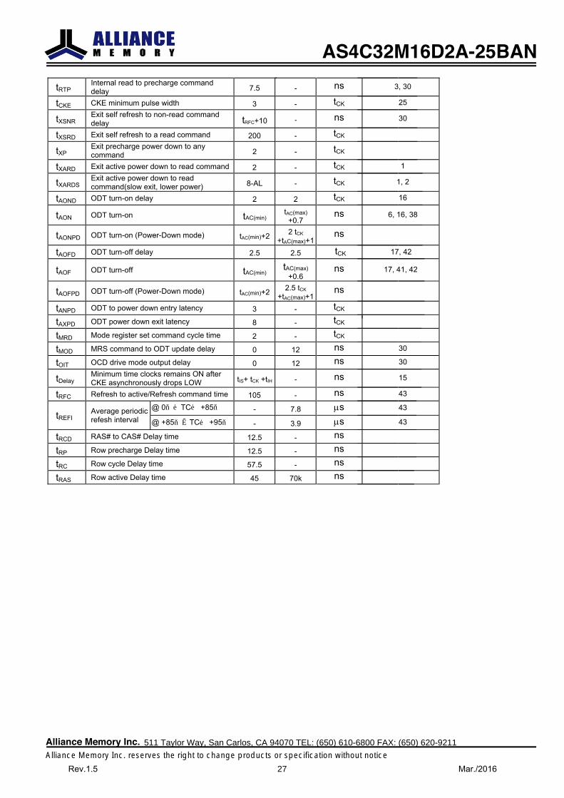
tRTP Internal read to precharge command delay 7.5 - ns 3, 30
tCKE CKE minimum pulse width 3 - tCK 25
tXSNR Exit self refresh to non-read command delay tRFC+10 - ns 30
tXSRD Exit self refresh to a read command 200 - tCK
tXP Exit precharge power down to any command 2 - tCK
tXARD Exit active power down to read command 2 - tCK 1
tXARDS Exit active power down to read command(slow exit, lower power) 8-AL - tCK 1, 2
tAOND ODT turn-on delay 2 2 tCK 16
tAON ODT turn-on tAC(min)tAC(max) +0.7
ns 6, 16, 38
tAONPD ODT turn-on (Power-Down mode) tAC(min)+2 2 tCK +tAC(max)+1
ns
tAOFD ODT turn-off delay 2.5 2.5 17, 42
tAOF ODT turn-off tAC(min)tAC(max)
+0.6 ns 17, 41, 42
tAOFPD ODT turn-off (Power-Down mode) tAC(min)+2 2.5 tCK +tAC(max)+1
ns
tANPD ODT to power down entry latency 3 - tCK
tAXPD ODT power down exit latency 8 - tCK
tMRD Mode register set command cycle time 2 - tCK
tMOD MRS command to ODT update delay 0 12 ns 30
tOIT OCD drive mode output delay 0 12 ns 30
tDelay Minimum time clocks remains ON after CKE asynchronously drops LOW tIS+ tCK +tIH - ns 15
tRFC Refresh to active/Refresh command time 105 - ns 43
tREFI Average periodic refesh interval
@ 0≦TC≦ +85 - 7.8 µs 43
@ +85<TC≦ +95 - 3.9 µs 43
tRCD RAS# to CAS# Delay time 12.5 - nstRP Row precharge Delay time 12.5 - nstRC Row cycle Delay time 57.5 - nstRAS Row active Delay time 45 70k ns
AS4C32M16D2A-25BAN
Alliance Memory Inc. 511 Taylor Way, San Carlos, CA 94070 TEL: (650) 610-6800 FAX: (650) 620-9211
Alliance Memory Inc. reserves the right to change products or specification without noticeRev.1.5 27 Mar./2016
tCK
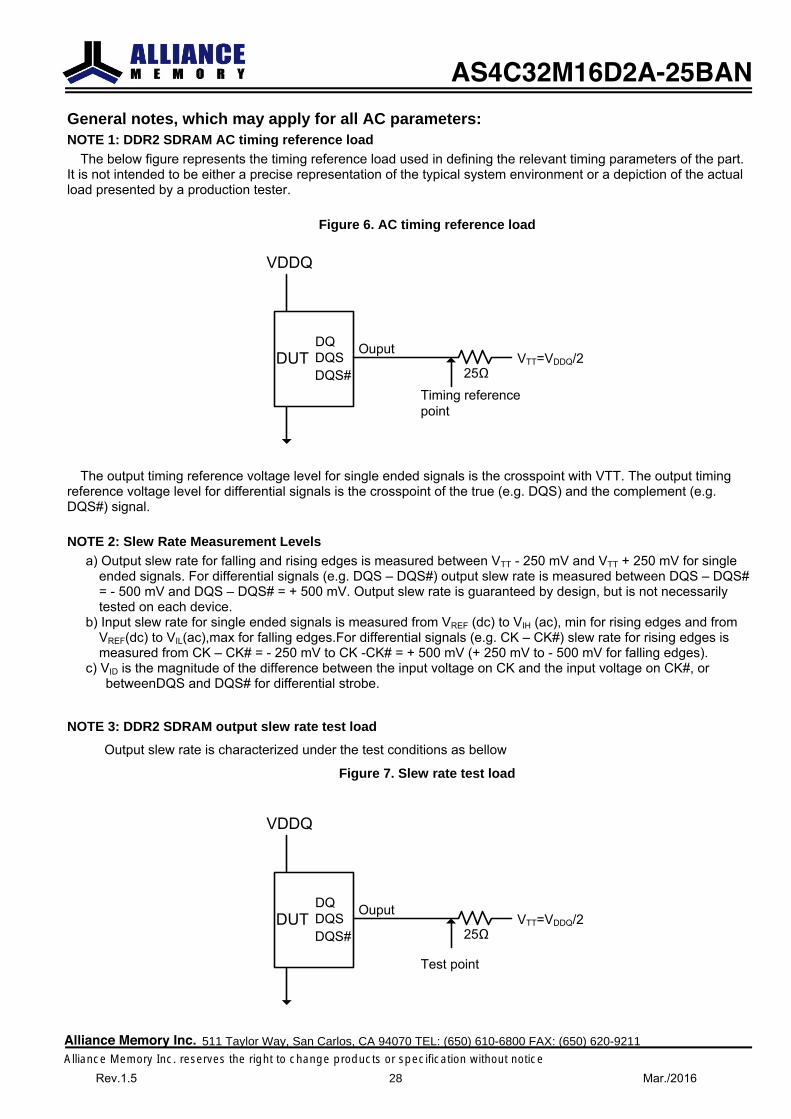
General notes, which may apply for all AC parameters: NOTE 1: DDR2 SDRAM AC timing reference load
The below figure represents the timing reference load used in defining the relevant timing parameters of the part. It is not intended to be either a precise representation of the typical system environment or a depiction of the actual load presented by a production tester.
Figure 6. AC timing reference load
VDDQ
DUT DQSDQS#
DQVTT=VDDQ/2
25ΩTiming reference point
Ouput
The output timing reference voltage level for single ended signals is the crosspoint with VTT. The output timing reference voltage level for differential signals is the crosspoint of the true (e.g. DQS) and the complement (e.g. DQS#) signal.
NOTE 2: Slew Rate Measurement Levels a) Output slew rate for falling and rising edges is measured between VTT - 250 mV and VTT + 250 mV for single
ended signals. For differential signals (e.g. DQS – DQS#) output slew rate is measured between DQS – DQS# = - 500 mV and DQS – DQS# = + 500 mV. Output slew rate is guaranteed by design, but is not necessarily tested on each device.
b) Input slew rate for single ended signals is measured from VREF (dc) to VIH (ac), min for rising edges and fromVREF(dc) to VIL(ac),max for falling edges.For differential signals (e.g. CK – CK#) slew rate for rising edges is measured from CK – CK# = - 250 mV to CK -CK# = + 500 mV (+ 250 mV to - 500 mV for falling edges).
c) VID is the magnitude of the difference between the input voltage on CK and the input voltage on CK#, orbetweenDQS and DQS# for differential strobe.
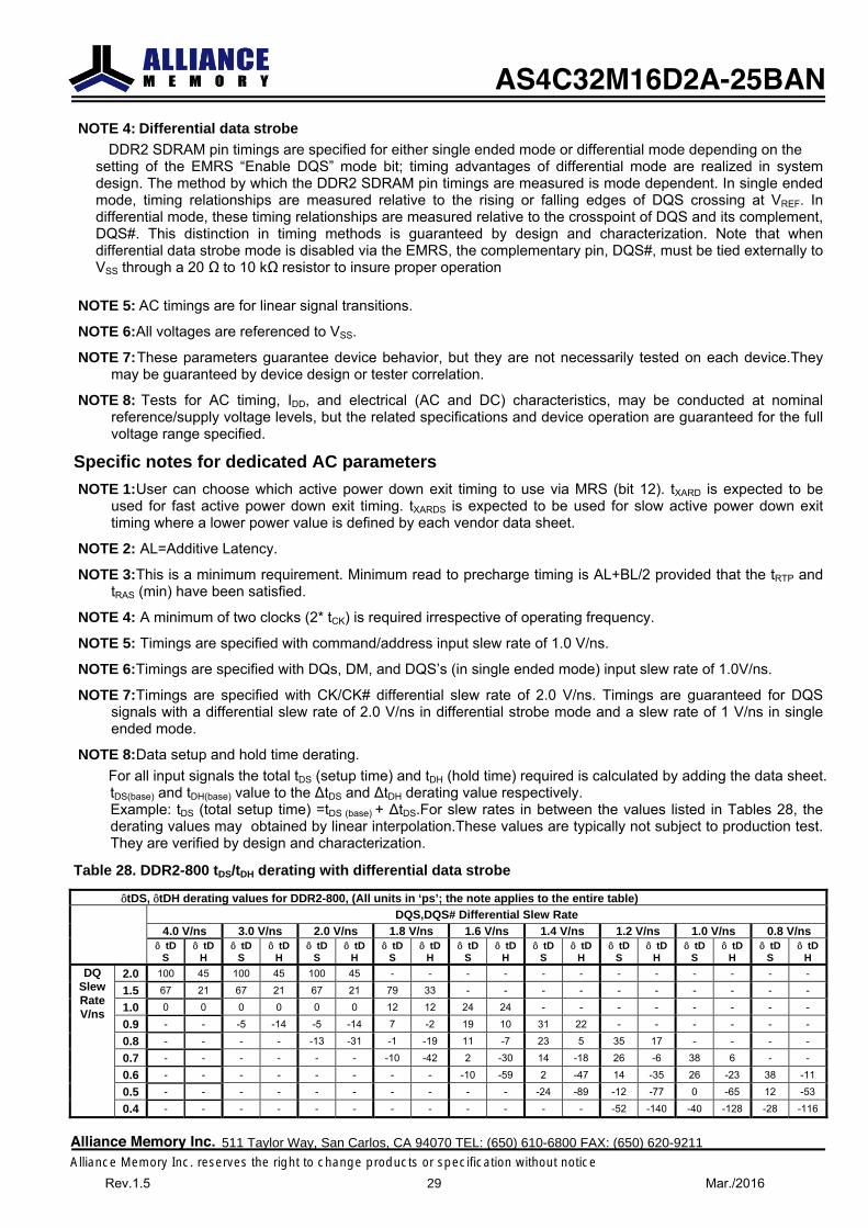
NOTE 3: DDR2 SDRAM output slew rate test load
Output slew rate is characterized under the test conditions as bellow
Figure 7. Slew rate test load
VDDQ
DUT DQSDQS#
DQVTT=VDDQ/2
25Ω
Test point
Ouput
AS4C32M16D2A-25BAN
Alliance Memory Inc. 511 Taylor Way, San Carlos, CA 94070 TEL: (650) 610-6800 FAX: (650) 620-9211
Alliance Memory Inc. reserves the right to change products or specification without noticeRev.1.5 28 Mar./2016
NOTE 4: Differential data strobe DDR2 SDRAM pin timings are specified for either single ended mode or differential mode depending on the
setting of the EMRS “Enable DQS” mode bit; timing advantages of differential mode are realized in system design. The method by which the DDR2 SDRAM pin timings are measured is mode dependent. In single ended mode, timing relationships are measured relative to the rising or falling edges of DQS crossing at VREF. In differential mode, these timing relationships are measured relative to the crosspoint of DQS and its complement, DQS#. This distinction in timing methods is guaranteed by design and characterization. Note that when differential data strobe mode is disabled via the EMRS, the complementary pin, DQS#, must be tied externally to VSS through a 20 Ω to 10 kΩ resistor to insure proper operation
NOTE 5: AC timings are for linear signal transitions.
NOTE 6: All voltages are referenced to VSS.
NOTE 7: These parameters guarantee device behavior, but they are not necessarily tested on each device.They may be guaranteed by device design or tester correlation.
NOTE 8: Tests for AC timing, IDD, and electrical (AC and DC) characteristics, may be conducted at nominal reference/supply voltage levels, but the related specifications and device operation are guaranteed for the full voltage range specified.
Specific notes for dedicated AC parameters NOTE 1: User can choose which active power down exit timing to use via MRS (bit 12). tXARD is expected to be
used for fast active power down exit timing. tXARDS is expected to be used for slow active power down exit timing where a lower power value is defined by each vendor data sheet.
NOTE 2: AL=Additive Latency.
NOTE 3: This is a minimum requirement. Minimum read to precharge timing is AL+BL/2 provided that the tRTP and tRAS (min) have been satisfied.
NOTE 4: A minimum of two clocks (2* tCK) is required irrespective of operating frequency.
NOTE 5: Timings are specified with command/address input slew rate of 1.0 V/ns.
NOTE 6: Timings are specified with DQs, DM, and DQS’s (in single ended mode) input slew rate of 1.0V/ns.
NOTE 7: Timings are specified with CK/CK# differential slew rate of 2.0 V/ns. Timings are guaranteed for DQS signals with a differential slew rate of 2.0 V/ns in differential strobe mode and a slew rate of 1 V/ns in single ended mode.
NOTE 8: Data setup and hold time derating. For all input signals the total tDS (setup time) and tDH (hold time) required is calculated by adding the data sheet.
tDS(base) and tDH(base) value to the ∆tDS and ∆tDH derating value respectively. Example: tDS (total setup time) =tDS (base) + ∆tDS.For slew rates in between the values listed in Tables 28, the derating values may obtained by linear interpolation.These values are typically not subject to production test. They are verified by design and characterization.
Table 28. DDR2-800 tDS/tDH derating with differential data strobe
tDS, tDH derating values for DDR2-800, (All units in ‘ps’; the note applies to the entire table) DQS,DQS# Differential Slew Rate
4.0 V/ns 3.0 V/ns 2.0 V/ns 1.8 V/ns 1.6 V/ns 1.4 V/ns 1.2 V/ns 1.0 V/ns 0.8 V/ns tD
S tD
H tD
S tD
H tD
S tD
H tD
S tD
H tD
S tD
H tD
S tD
H tD
S tD
H tD
S tD
H tD
S tD
H DQ
Slew Rate V/ns
2.0 100 45 100 45 100 45 - - - - - - - - - - - -
1.5 67 21 67 21 67 21 79 33 - - - - - - - - - -
1.0 0 0 0 0 0 0 12 12 24 24 - - - - - - - -
0.9 - - -5 -14 -5 -14 7 -2 19 10 31 22 - - - - - -
0.8 - - - - -13 -31 -1 -19 11 -7 23 5 35 17 - - - -
0.7 - - - - - - -10 -42 2 -30 14 -18 26 -6 38 6 - -
0.6 - - - - - - - - -10 -59 2 -47 14 -35 26 -23 38 -11
0.5 - - - - - - - - - - -24 -89 -12 -77 0 -65 12 -53
0.4 - - - - - - - - - - - - -52 -140 -40 -128 -28 -116
AS4C32M16D2A-25BAN
Alliance Memory Inc. 511 Taylor Way, San Carlos, CA 94070 TEL: (650) 610-6800 FAX: (650) 620-9211
Alliance Memory Inc. reserves the right to change products or specification without noticeRev.1.5 29 Mar./2016
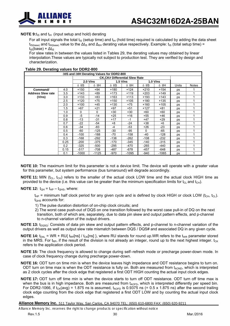
NOTE 9: tIS and tIH (input setup and hold) derating For all input signals the total tIS (setup time) and tIH (hold time) required is calculated by adding the data sheet tIS(base) and tIH(base) value to the ∆tIS and ∆tIH derating value respectively. Example: tIS (total setup time) = tIS(base) + ∆tIS For slew rates in between the values listed in Tables 29, the derating values may obtained by linear interpolation.These values are typically not subject to production test. They are verified by design and characterization.
Table 29. Derating values for DDR2-800tIS and tIH Derating Values for DDR2-800
CK,CK# Differential Slew Rate 2.0 V/ns 1.5 V/ns 1.0 V/ns
tIS tIH tIS tIH tIS tIH Units Notes Command/
Address Slew rate (V/ns)
4.0 +150 +94 +180 +124 +210 +154 ps 1 3.5 +143 +89 +173 +119 +203 +149 ps 1 3.0 +133 +83 +163 +113 +193 +143 ps 1 2.5 +120 +75 +150 +105 +180 +135 ps 1 2.0 +100 +45 +130 +75 +160 +105 ps 1 1.5 +67 +21 +97 +51 +127 +81 ps 1 1.0 0 0 +30 +30 +60 +60 ps 10.9 -5 -14 +25 +16 +55 +46 ps 1 0.8 -13 -31 +17 -1 +47 +29 ps 1 0.7 -22 -54 +8 -24 +38 +6 ps 1 0.6 -34 -83 -4 -53 +26 -23 ps 1 0.5 -60 -125 -30 -95 0 -65 ps 1 0.4 -100 -188 -70 -158 -40 -128 ps 1 0.3 -168 -292 -138 -262 -108 -232 ps 1
0.25 -200 -375 -170 -345 -140 -315 ps 1 0.2 -325 -500 -295 -470 -265 -440 ps 1
0.15 -517 -708 -487 -678 -457 -648 ps 1 0.1 -1000 -1125 -970 -1095 -940 -1065 ps 1
NOTE 10: The maximum limit for this parameter is not a device limit. The device will operate with a greater value for this parameter, but system performance (bus turnaround) will degrade accordingly.
NOTE 11: MIN (tCL, tCH) refers to the smaller of the actual clock LOW time and the actual clock HIGH time as provided to the device (i.e. this value can be greater than the minimum specification limits for tCL and tCH).
NOTE 12: tQH = tHP – tQHS, where:
tHP = minimum half clock period for any given cycle and is defined by clock HIGH or clock LOW (tCH, tCL). tQHS accounts for: 1) The pulse duration distortion of on-chip clock circuits; and2) The worst case push-out of DQS on one transition followed by the worst case pull-in of DQ on the nexttransition, both of which are, separately, due to data pin skew and output pattern effects, and p-channel to n-channel variation of the output drivers.
NOTE 13: tDQSQ: Consists of data pin skew and output pattern effects, and p-channel to n-channel variation of the output drivers as well as output slew rate mismatch between DQS / DQS# and associated DQ in any given cycle.
NOTE 14: tDAL = WR + RU tRP[ns] / tCK[ns] , where RU stands for round up.WR refers to the tWR parameter stored in the MRS. For tRP, if the result of the division is not already an integer, round up to the next highest integer. tCK refers to the application clock period.
NOTE 15: The clock frequency is allowed to change during self–refresh mode or precharge power-down mode. In case of clock frequency change during precharge power-down.
NOTE 16: ODT turn on time min is when the device leaves high impedance and ODT resistance begins to turn on. ODT turn on time max is when the ODT resistance is fully on. Both are measured from tAOND, which is interpreted as 2 clock cycles after the clock edge that registered a first ODT HIGH counting the actual input clock edges.
NOTE 17: ODT turn off time min is when the device starts to turn off ODT resistance. ODT turn off time max is when the bus is in high impedance. Both are measured from tAOFD, which is interpreted differently per speed bin. For DDR2-1066, if tCK(avg) = 1.875 ns is assumed, tAOFD is 0.9375 ns (= 0.5 x 1.875 ns) after the second trailing clock edge counting from the clock edge that registered a first ODT LOW and by counting the actual input clock edges.
AS4C32M16D2A-25BAN
Alliance Memory Inc. 511 Taylor Way, San Carlos, CA 94070 TEL: (650) 610-6800 FAX: (650) 620-9211
Alliance Memory Inc. reserves the right to change products or specification without noticeRev.1.5 30 Mar./2016
NOTE 18: tHZ and tLZ transitions occur in the same access time as valid data transitions. These parameters are referenced to a specific voltage level which specifies when the device output is no longer driving (tHZ), or begins driving (tLZ).
NOTE 19: tRPST end point and tRPRE begin point are not referenced to a specific voltage level but specify when the device output is no longer driving (tRPST), or begins driving (tRPRE). The actual voltage measurement points are not critical as long as the calculation is consistent.
NOTE 20: Input waveform timing tDS with differential data strobe enabled MR[bit10]=0, is referenced from the input signal crossing at the VIH(ac) level to the differential data strobe crosspoint for a rising signal, and from the input signal crossing at the VIL(ac) level to the differential data strobe crosspoint for a falling signal applied to the device under test. DQS, DQS# signals must be monotonic between VIL(dc)max and VIH(dc)min.
NOTE 21: Input waveform timing tDH with differential data strobe enabled MR[bit10]=0, is referenced from the differential data strobe crosspoint to the input signal crossing at the VIH(dc) level for a falling signal and from the differential data strobe crosspoint to the input signal crossing at the VIL(dc) level for a rising signal applied to the device under test. DQS, DQS# signals must be monotonic between VIL(dc)max and VIH(dc)min.
NOTE 22: Input waveform timing is referenced from the input signal crossing at the VIH(ac) level for a rising signal and VIL(ac) for a falling signal applied to the device under test.
NOTE 23: Input waveform timing is referenced from the input signal crossing at the VIL(dc) level for a rising signal and VIH(dc) for a falling signal applied to the device under test.
NOTE 24: tWTR is at lease two clocks (2 x tCK ) independent of operation frequency.
NOTE 25: tCKEmin of 3 clocks means CKE must be registered on three consecutive positive clock edges. CKE must remain at the valid input level the entire time it takes to achieve the 3 clocks of registration. Thus, after any CKE transition, CKE may not transition from its valid level during the time period of tIS + 2 x tCK + tIH.
NOTE 26: If tDS or tDH is violated, data corruption may occur and the data must be re-written with valid data before a valid READ can be executed.
NOTE 27: These parameters are measured from a command/address signal (CKE, CS#, RAS#, CAS#, WE#, ODT, BA0, A0, A1, etc.) transition edge to its respective clock signal (CK/CK#) crossing. The spec values are not affected by the amount of clock jitter applied (i.e. tJIT(per), tJIT(cc), etc.), as the setup and hold are relative to the clock signal crossing that latches the command/address. That is, these parameters should be met whether clock jitter is present or not.
NOTE 28: These parameters are measured from a data strobe signal (LDQS/UDQS) crossing to its respective clock signal (CK/CK#) crossing. The spec values are not affected by the amount of clock jitter applied (i.e. tJIT(per), tJIT(cc), etc.), as these are relative to the clock signal crossing. That is, these parameters should be met whether clock jitter is present or not.
NOTE 29: These parameters are measured from a data signal ((L/U) DM, (L/U) DQ0, (L/U) DQ1, etc.) transition edge to its respective data strobe signal (LDQS/UDQS/LDQS#/UDQS#) crossing.
NOTE 30: For these parameters, the DDR2 SDRAM device is characterized and verified to support tnPARAM = RUtPARAM / tCK(avg), which is in clock cycles, assuming all input clock jitter specifications are satisfied.
NOTE 31: tDAL [tCK] = WR [tCK] + tRP [tCK] = WR + RU tRP [ps] / tCK(avg) [ps] , where WR is the value programmed in the mode register set.
NOTE 32: New units, ‘tCK(avg)’ is introduced in DDR2-800. Unit ‘tCK(avg)’ represents the actual tCK(avg) of the input clock under operation.
NOTE 33: Input clock jitter spec parameter. These parameters and the ones in the table below are referred to as 'input clock jitter spec parameters' and these parameters apply to DDR2-800 only. The jitter specified is a random jitter meeting a Gaussian distribution.
AS4C32M16D2A-25BAN
Alliance Memory Inc. 511 Taylor Way, San Carlos, CA 94070 TEL: (650) 610-6800 FAX: (650) 620-9211
Alliance Memory Inc. reserves the right to change products or specification without noticeRev.1.5 31 Mar./2016
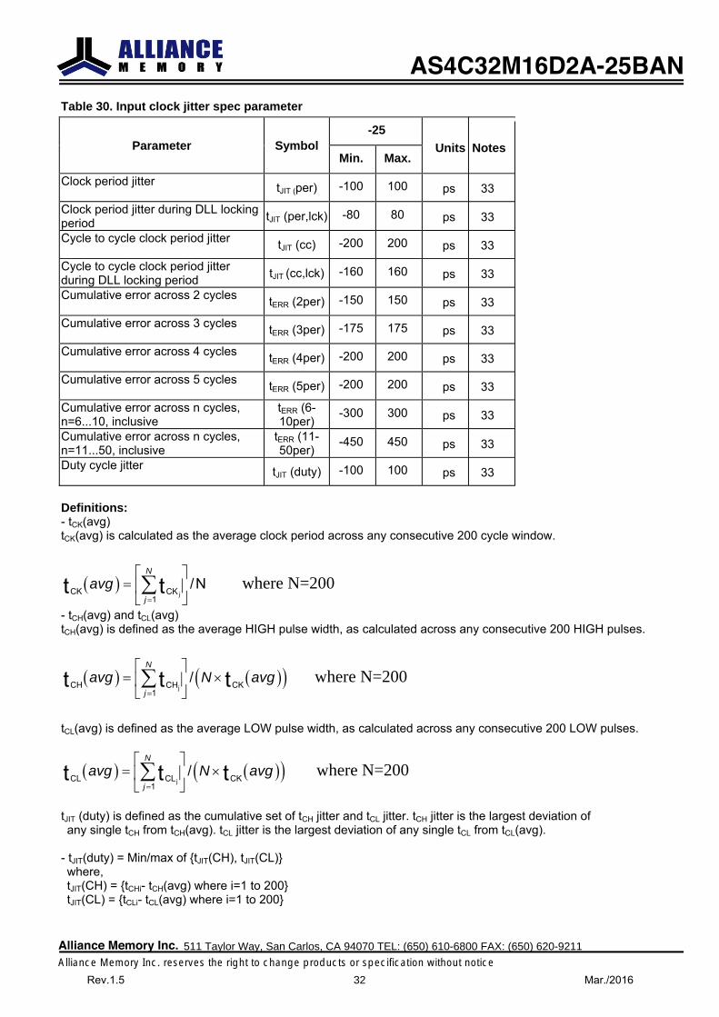
Table 30. Input clock jitter spec parameter
Parameter Symbol-25
Units NotesMin. Max.
Clock period jitter tJIT (per) -100 100 ps 33
Clock period jitter during DLL locking period tJIT (per,lck) -80 80 ps 33
Cycle to cycle clock period jitter tJIT (cc) -200 200 ps 33
Cycle to cycle clock period jitter during DLL locking period tJIT (cc,lck) -160 160 ps 33
Cumulative error across 2 cycles tERR (2per) -150 150 ps 33
Cumulative error across 3 cycles tERR (3per) -175 175 ps 33
Cumulative error across 4 cycles tERR (4per) -200 200 ps 33
Cumulative error across 5 cycles tERR (5per) -200 200 ps 33
Cumulative error across n cycles, n=6...10, inclusive
tERR (6-10per)
-300 300 ps 33
Cumulative error across n cycles, n=11...50, inclusive
tERR (11-50per)
-450 450 ps 33
Duty cycle jitter tJIT (duty) -100 100 ps 33
Definitions: - tCK(avg) tCK(avg) is calculated as the average clock period across any consecutive 200 cycle window.
( )=
⎡ ⎤= ⎢ ⎥⎣ ⎦∑
jCK CK1
/Nt tN
javg where N=200
- tCH(avg) and tCL(avg) tCH(avg) is defined as the average HIGH pulse width, as calculated across any consecutive 200 HIGH pulses.
( ) ( )( )=
⎡ ⎤= ×⎢ ⎥⎣ ⎦∑
jCH CH CK1
/t t tN
javg N avg where N=200
tCL(avg) is defined as the average LOW pulse width, as calculated across any consecutive 200 LOW pulses.
( ) ( )( )=
⎡ ⎤= ×⎢ ⎥⎣ ⎦∑
jCL CL CK1
/t t tN
javg N avg where N=200
tJIT (duty) is defined as the cumulative set of tCH jitter and tCL jitter. tCH jitter is the largest deviation of any single tCH from tCH(avg). tCL jitter is the largest deviation of any single tCL from tCL(avg).
- tJIT(duty) = Min/max of tJIT(CH), tJIT(CL) where, tJIT(CH) = tCHi- tCH(avg) where i=1 to 200 tJIT(CL) = tCLi- tCL(avg) where i=1 to 200
AS4C32M16D2A-25BAN
Alliance Memory Inc. 511 Taylor Way, San Carlos, CA 94070 TEL: (650) 610-6800 FAX: (650) 620-9211
Alliance Memory Inc. reserves the right to change products or specification without noticeRev.1.5 32 Mar./2016
- tJIT(per), tJIT(per,lck) tJIT(per) is defined as the largest deviation of any single tCK from tCK(avg). tJIT(per) = Min/max of tCKi- tCK(avg) where i=1 to 200 tJIT(per) defines the single period jitter when the DLL is already locked. tJIT(per,lck) uses the same definition for single period jitter, during the DLL locking period only. tJIT(per) and tJIT(per,lck) are not guaranteed through final production testing.
- tJIT(cc), tJIT(cc,lck) tJIT(cc) is defined as the difference in clock period between two consecutive clock cycles: tJIT(cc) = Max of |tCKi+1 – tCKi| tJIT(cc) defines the cycle to cycle jitter when the DLL is already locked. tJIT(cc,lck) uses the same definition for cycle to cycle jitter, during the DLL locking period only. tJIT(cc) and tJIT(cc,lck) are not guaranteed through final production testing.
- tERR(2per), tERR (3per), tERR (4per), tERR (5per), tERR (6-10per) and tERR (11-50per) tERR is defined as the cumulative error across multiple consecutive cycles from tCK(avg).
( ) ( )( )+ −
=
⎡ ⎤= − ×⎢ ⎥⎣ ⎦∑
j
1
ERR CK CK1
npert t ti N
jN avg where
( )( )( )( )( )( )
⎧⎪⎪⎪⎪⎨⎪⎪ ≤ ≤ −⎪⎪ ≤ ≤ −⎩
ERR
ERR
ERR
ERR
ERR
ERR
n=2 for 2
n=3 for 3
n=4 for 4
n=5 for 5
6 n 10 for 6 10
11 n 50 for 11 50
tttttt
per
per
per
per
per
per
NOTE 34: These parameters are specified per their average values, however it is understood that the following relationship between the average timing and the absolute instantaneous timing holds at all times. (Min andmax of SPEC values are to be used for calculations in the table below.)
Table 31. Absolute clock period average values Parameter Symbol Min. Max. Units
Absolute clock period tCK (abs) tCK(avg),min + tJIT(per),min tCK(avg),max + tJIT(per),max ps
Absolute clock HIGH pulse width tCH (abs) tCH(avg),min * tCK(avg),min + tJIT(duty),min
tCH(avg),max * tCK(avg),max + tJIT(duty),max
ps
Absolute clock LOW pulse width tCL (abs) tCL(avg),min * tCK(avg),min + tJIT(duty),min
tCL(avg), max * tCK(avg),max + tJIT(duty), max
ps
NOTE 35: tHP is the minimum of the absolute half period of the actual input clock. tHP is an input parameter but not an input specification parameter. It is used in conjunction with tQHS to derive the DRAM output timing tQH. The value to be used for tQH calculation is determined by the following equation;
tHP = Min ( tCH(abs), tCL(abs) ),
where,
tCH(abs) is the minimum of the actual instantaneous clock HIGH time;
tCL(abs) is the minimum of the actual instantaneous clock LOW time;
NOTE 36: tQHS accounts for: 1) The pulse duration distortion of on-chip clock circuits, which represents how well the actual tHP at the input
is transferred to the output; and2) The worst case push-out of DQS on one transition followed by the worst case pull-in of DQ on the next
transition, both of which are independent of each other, due to data pin skew, output pattern effects, and p-channel to n-channel variation of the output drivers
AS4C32M16D2A-25BAN
Alliance Memory Inc. 511 Taylor Way, San Carlos, CA 94070 TEL: (650) 610-6800 FAX: (650) 620-9211
Alliance Memory Inc. reserves the right to change products or specification without noticeRev.1.5 33 Mar./2016
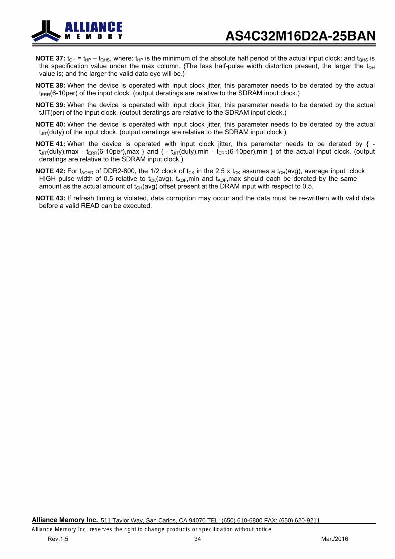
NOTE 37: tQH = tHP – tQHS, where: tHP is the minimum of the absolute half period of the actual input clock; and tQHS is the specification value under the max column. The less half-pulse width distortion present, the larger the tQH value is; and the larger the valid data eye will be.
NOTE 38: When the device is operated with input clock jitter, this parameter needs to be derated by the actual tERR(6-10per) of the input clock. (output deratings are relative to the SDRAM input clock.)
NOTE 39: When the device is operated with input clock jitter, this parameter needs to be derated by the actual tJIT(per) of the input clock. (output deratings are relative to the SDRAM input clock.)
NOTE 40: When the device is operated with input clock jitter, this parameter needs to be derated by the actual tJIT(duty) of the input clock. (output deratings are relative to the SDRAM input clock.)
NOTE 41: When the device is operated with input clock jitter, this parameter needs to be derated by - tJIT(duty),max - tERR(6-10per),max and - tJIT(duty),min - tERR(6-10per),min of the actual input clock. (output deratings are relative to the SDRAM input clock.)
NOTE 42: For tAOFD of DDR2-800, the 1/2 clock of tCK in the 2.5 x tCK assumes a tCH(avg), average input clock HIGH pulse width of 0.5 relative to tCK(avg). tAOF,min and tAOF,max should each be derated by the same amount as the actual amount of tCH(avg) offset present at the DRAM input with respect to 0.5.
NOTE 43: If refresh timing is violated, data corruption may occur and the data must be re-writtern with valid data before a valid READ can be executed.
AS4C32M16D2A-25BAN
Alliance Memory Inc. 511 Taylor Way, San Carlos, CA 94070 TEL: (650) 610-6800 FAX: (650) 620-9211
Alliance Memory Inc. reserves the right to change products or specification without noticeRev.1.5 34 Mar./2016
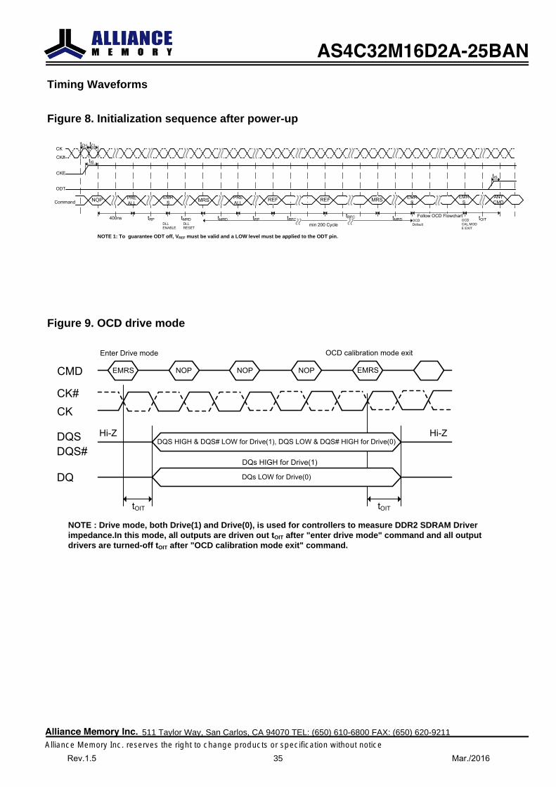
Timing Waveforms
Figure 8. Initialization sequence after power-up
CK
CK#
tCH
CKE
Command
tCL
tIS
ODT
tIS
NOP PREALL
EMRS MRS PRE
ALL REF REF MRS EMRS
EMRS
ANYCMD
400ns tRP tMRD tMRD tRP tMRDFollow OCD Flowchart tOIT
min 200 CycleDLL ENABLE
DLL RESET
OCD Default
OCD CAL.MODE EXIT
NOTE 1: To guarantee ODT off, VREF must be valid and a LOW level must be applied to the ODT pin.
tRFCtRFC
Figure 9. OCD drive mode
CK#
Hi-Z
CK
DQSDQS#
DQs HIGH for Drive(1)
CMD
OCD calibration mode exit
tOIT
Enter Drive mode
EMRS NOP NOP NOP EMRS
DQ
DQS HIGH & DQS# LOW for Drive(1), DQS LOW & DQS# HIGH for Drive(0)
DQs LOW for Drive(0)
tOIT
Hi-Z
NOTE : Drive mode, both Drive(1) and Drive(0), is used for controllers to measure DDR2 SDRAM Driver impedance.In this mode, all outputs are driven out tOIT after "enter drive mode" command and all output drivers are turned-off tOIT after "OCD calibration mode exit" command.
AS4C32M16D2A-25BAN
Alliance Memory Inc. 511 Taylor Way, San Carlos, CA 94070 TEL: (650) 610-6800 FAX: (650) 620-9211
Alliance Memory Inc. reserves the right to change products or specification without noticeRev.1.5 35 Mar./2016
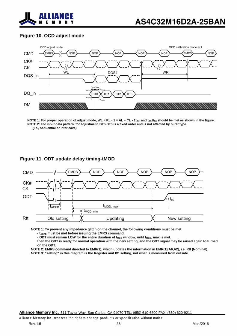
Figure 10. OCD adjust mode
CK#
WLCK
DQS_in
DQ_in
DQS#
tDS tDH
CMDOCD calibration mode exit
WR
OCD adjust mode
EMRS NOP NOP NOP NOP NOP EMRS NOP
DT0 DT1 DT3DT2VIH(ac)
VIL(ac)
VIH(dc)
VIL(dc)
DM
NOTE 1: For proper operation of adjust mode, WL = RL - 1 = AL + CL - 1tCK and tDS /tDH should be met as shown in the figure. NOTE 2: For input data pattern for adjustment, DT0-DT3 is a fixed order and is not affected by burst type
(i.e., sequential or interleave)
Figure 11. ODT update delay timing-tMOD
CK
UpdatingRtt
tIS
EMRS NOP NOP NOP NOP NOPCMD
tAOFD tMOD, maxtMOD, min
Old setting New setting
ODT
NOTE 1: To prevent any impedance glitch on the channel, the following conditions must be met:- tAOFD must be met before issuing the EMRS command.- ODT must remain LOW for the entire duration of tMOD window, until tMOD, max is met.
then the ODT is ready for normal operation with the new setting, and the ODT signal may be raised again to turned on the ODT.
NOTE 2: EMRS command directed to EMR(1), which updates the information in EMR(1)[A6,A2], i.e. Rtt (Nominal).NOTE 3: "setting" in this diagram is the Register and I/O setting, not what is measured from outside.
CK#
AS4C32M16D2A-25BAN
Alliance Memory Inc. 511 Taylor Way, San Carlos, CA 94070 TEL: (650) 610-6800 FAX: (650) 620-9211
Alliance Memory Inc. reserves the right to change products or specification without noticeRev.1.5 36 Mar./2016
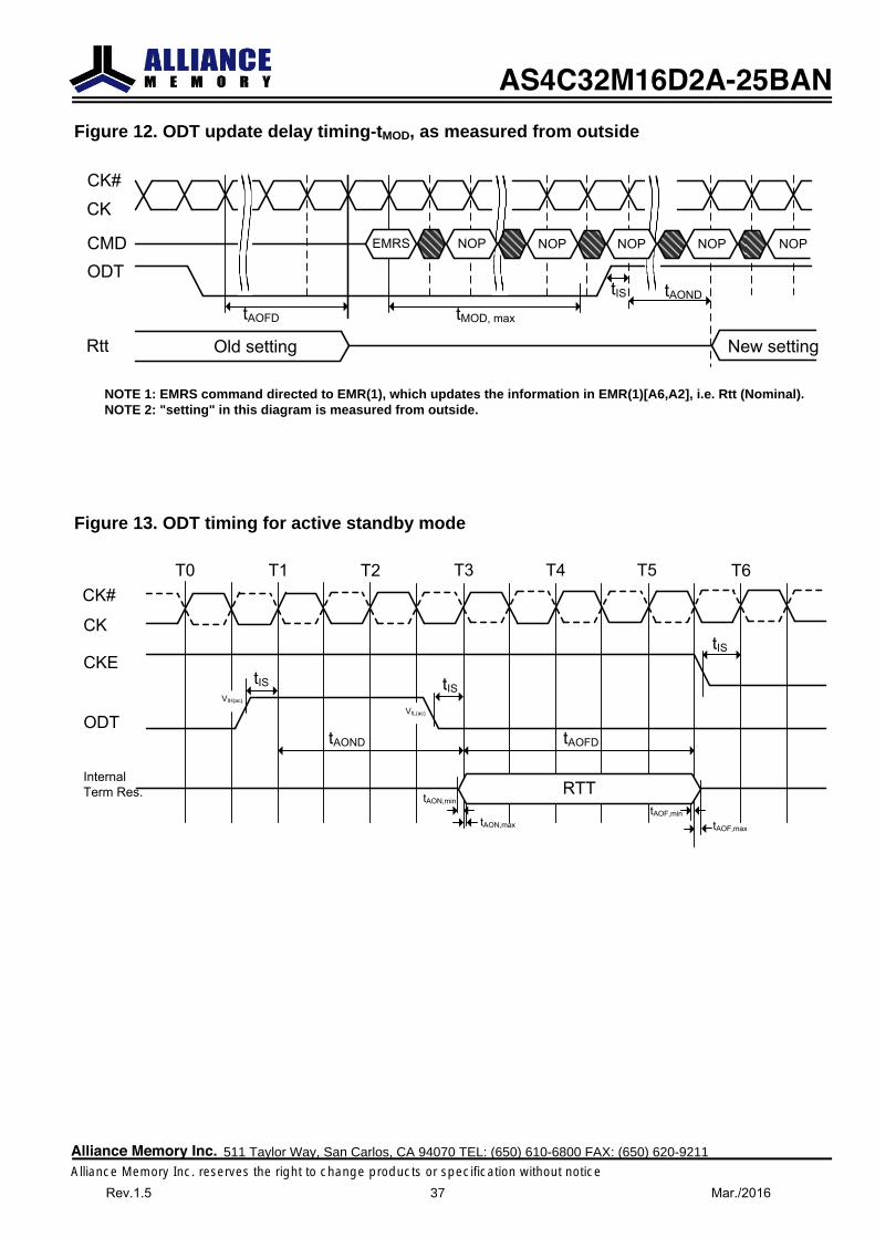
Figure 12. ODT update delay timing-tMOD, as measured from outside
CK#CK
Rtt
tIS
EMRSCMD
tAOFD tMOD, max
Old setting New setting
ODT
NOP NOP NOP NOP NOP
tAOND
NOTE 1: EMRS command directed to EMR(1), which updates the information in EMR(1)[A6,A2], i.e. Rtt (Nominal).NOTE 2: "setting" in this diagram is measured from outside.
Figure 13. ODT timing for active standby mode
CK#T0
InternalTerm Res.
tIS
tIS
tAOND
CK
T1 T2 T3 T4 T5 T6
CKE
ODTVIH(ac)
tISVIL(ac)
tAOFD
tAON,min
tAON,max
tAOF,min
tAOF,max
RTT
AS4C32M16D2A-25BAN
Alliance Memory Inc. 511 Taylor Way, San Carlos, CA 94070 TEL: (650) 610-6800 FAX: (650) 620-9211
Alliance Memory Inc. reserves the right to change products or specification without noticeRev.1.5 37 Mar./2016
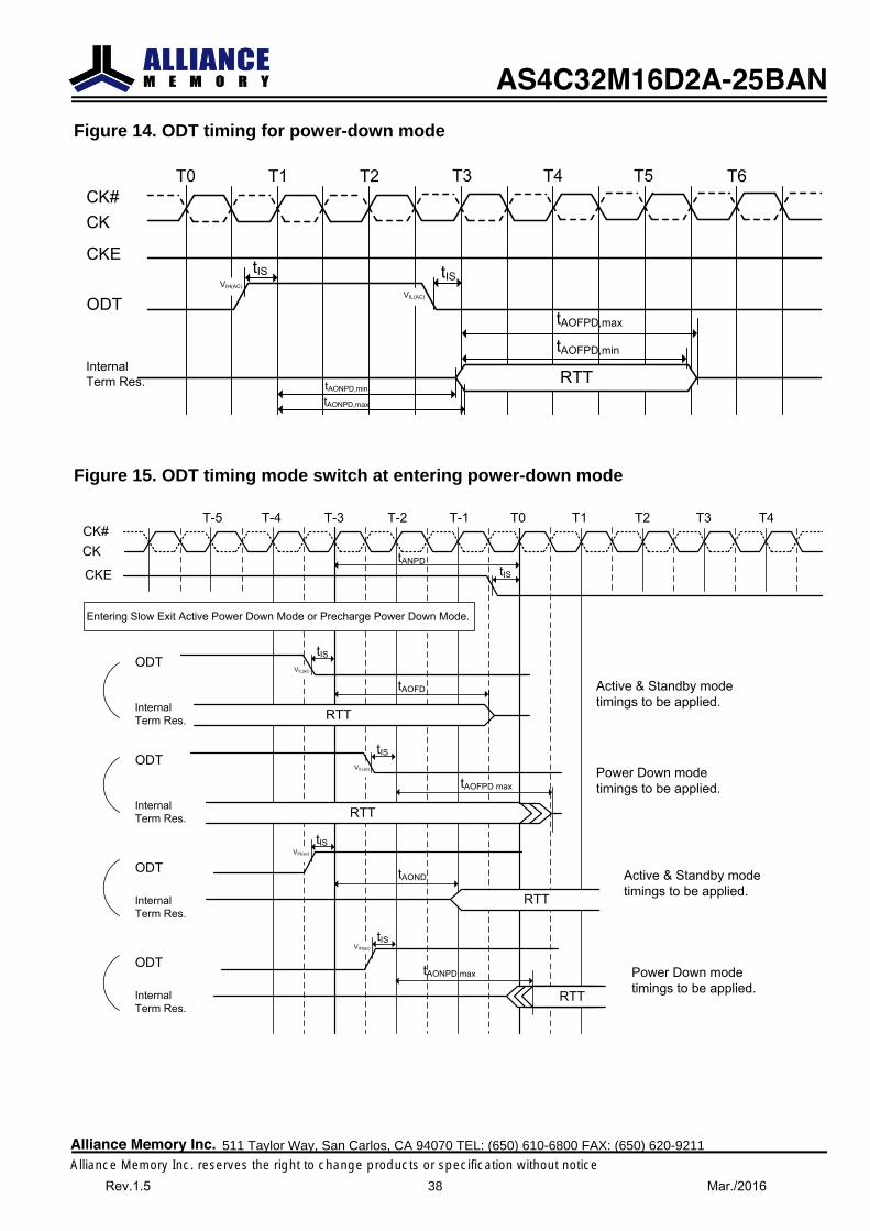
Figure 14. ODT timing for power-down mode
CK#T0
InternalTerm Res.
tIS
CK
T1 T2 T3 T4 T5 T6
CKE
ODTVIH(AC)
tISVIL(AC)
tAOFPD,max
tAONPD,minRTT
tAOFPD,min
tAONPD,max
Figure 15. ODT timing mode switch at entering power-down mode
CK#CK
tISCKE
tAOFD
tAOND
ODT
tANPD
T-5 T-4 T-3 T-2 T-1 T0 T1 T2 T3 T4
Entering Slow Exit Active Power Down Mode or Precharge Power Down Mode.
RTTInternalTerm Res.
tISVIL(ac)
ODT
RTTInternalTerm Res.
tISVIL(ac)
tAOFPD max
Active & Standby mode timings to be applied.
Power Down mode timings to be applied.
tISVIH(ac)
RTT
Active & Standby mode timings to be applied.
tAONPD max
tISVIH(ac)
Power Down mode timings to be applied.RTT
ODT
ODT
InternalTerm Res.
InternalTerm Res.
AS4C32M16D2A-25BAN
Alliance Memory Inc. 511 Taylor Way, San Carlos, CA 94070 TEL: (650) 610-6800 FAX: (650) 620-9211
Alliance Memory Inc. reserves the right to change products or specification without noticeRev.1.5 38 Mar./2016
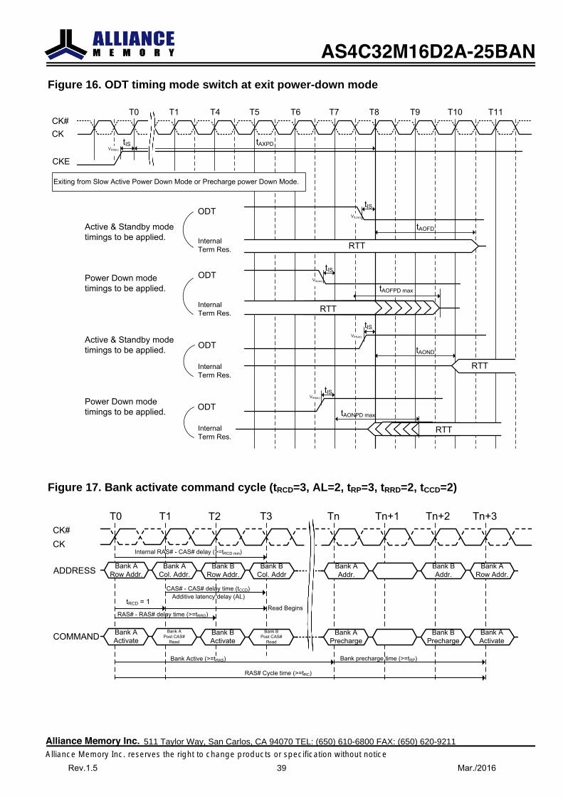
Figure 16. ODT timing mode switch at exit power-down mode
CK#CK
tIS
CKE
tAOFD
tAOND
ODT
tAXPD
T0 T1 T4 T5 T6 T7 T8 T9 T10 T11
Exiting from Slow Active Power Down Mode or Precharge power Down Mode.
InternalTerm Res.
tISVIL(ac)
ODT
InternalTerm Res.
tISVIL(ac)
Active & Standby mode timings to be applied.
Power Down mode timings to be applied.
tIS
VIH(ac)
Active & Standby mode timings to be applied.
tAONPD max
tISVIH(ac)Power Down mode
timings to be applied.
ODT
ODT
InternalTerm Res.
InternalTerm Res.
RTT
tAOFPD max
VIH(ac)
RTT
RTT
RTT
Figure 17. Bank activate command cycle (tRCD=3, AL=2, tRP=3, tRRD=2, tCCD=2)
CK#T0 T1 T2 T3 Tn Tn+1 Tn+2
Internal RAS# - CAS# delay (>=tRCD min)
CAS# - CAS# delay time (tCCD)
tRCD = 1Read Begins
Tn+3
Bank ARow Addr.
Bank ACol. Addr.
Bank BRow Addr.
Bank BCol. Addr
Bank AAddr.
Bank BAddr.
Bank ARow Addr.
Additive latency delay (AL)
Bank AActivate
Bank APost CAS#
Read
Bank BActivate
Bank BPost CAS#
Read
Bank APrecharge
Bank BPrecharge
Bank AActivate
RAS# - RAS# delay time (>=tRRD)
Bank Active (>=tRAS) Bank precharge time (>=tRP)
RAS# Cycle time (>=tRC)
ADDRESS
COMMAND
CK
AS4C32M16D2A-25BAN
Alliance Memory Inc. 511 Taylor Way, San Carlos, CA 94070 TEL: (650) 610-6800 FAX: (650) 620-9211
Alliance Memory Inc. reserves the right to change products or specification without noticeRev.1.5 39 Mar./2016
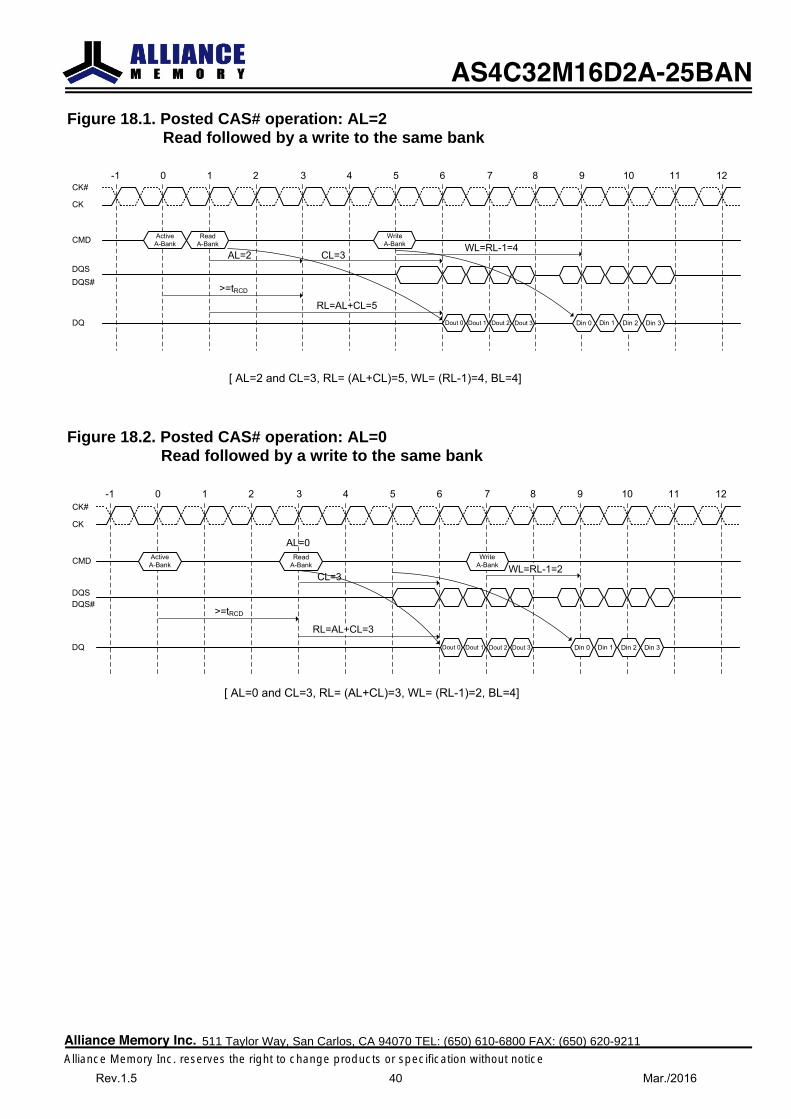
Figure 18.1. Posted CAS# operation: AL=2 Read followed by a write to the same bank
CK#
CMD
AL=2
-1 1 2 3 4 5 6 7 8 90 10 11 12
ActiveA-Bank
ReadA-Bank
WriteA-Bank
CL=3WL=RL-1=4
Dout 0 Dout 1 Dout 2 Dout 3 Din 0 Din 1 Din 2 Din 3
RL=AL+CL=5
>=tRCD
[ AL=2 and CL=3, RL= (AL+CL)=5, WL= (RL-1)=4, BL=4]
DQS
DQ
CK
DQS#
Figure 18.2. Posted CAS# operation: AL=0 Read followed by a write to the same bank
CK#
CMD
AL=0
-1 1 2 3 4 5 6 7 8 90 10 11 12
ActiveA-Bank
ReadA-Bank
WriteA-Bank
CL=3WL=RL-1=2
Dout 0 Dout 1 Dout 2 Dout 3 Din 0 Din 1 Din 2 Din 3
RL=AL+CL=3
>=tRCD
[ AL=0 and CL=3, RL= (AL+CL)=3, WL= (RL-1)=2, BL=4]
DQS
DQ
CK
DQS#
AS4C32M16D2A-25BAN
Alliance Memory Inc. 511 Taylor Way, San Carlos, CA 94070 TEL: (650) 610-6800 FAX: (650) 620-9211
Alliance Memory Inc. reserves the right to change products or specification without noticeRev.1.5 40 Mar./2016
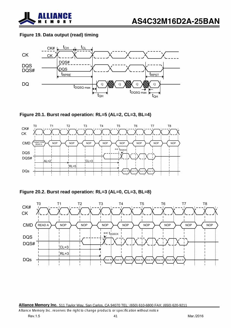
Figure 19. Data output (read) timing
CK#
CK
DQ tDQSQ max
CK
tCH
tRPSTtRPRE
DQS
tCL
DQS#
DQS
Q Q Q
tQH
Q
tQHtDQSQ max
DQS#
Figure 20.1. Burst read operation: RL=5 (AL=2, CL=3, BL=4)
CKCK#
DQs
CMD
DQS
T0 T1 T2 T3 T4 T5 T6 T7 T8
Posted CAS#READ A NOP NOP NOP NOP NOP NOP NOP NOP
=< tDQSCK
Dout A0 Dout A1 Dout A2 Dout A3
AL=2 CL=3
RL=5
DQS#
Figure 20.2. Burst read operation: RL=3 (AL=0, CL=3, BL=8)
CKCK#
DQs
CMD
DQS
T0 T1 T2 T3 T4 T5 T6 T7 T8
READ A NOP NOP NOP NOP NOP NOP NOP NOP
Dout A0 Dout A1 Dout A2 Dout A3
CL=3
RL=3
DQS#
=< tDQSCK
Dout A4 Dout A5 Dout A6 Dout A7
AS4C32M16D2A-25BAN
Alliance Memory Inc. 511 Taylor Way, San Carlos, CA 94070 TEL: (650) 610-6800 FAX: (650) 620-9211
Alliance Memory Inc. reserves the right to change products or specification without noticeRev.1.5 41 Mar./2016
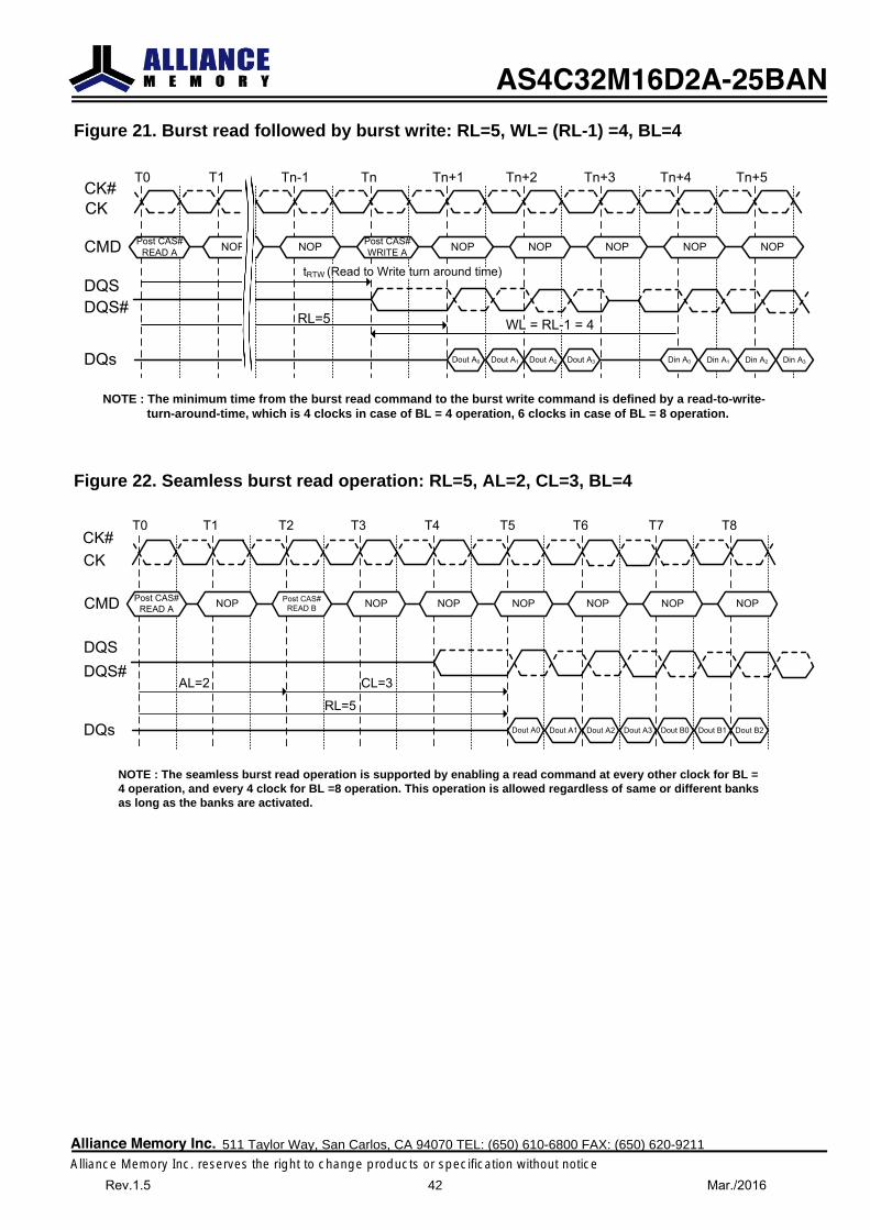
Figure 21. Burst read followed by burst write: RL=5, WL= (RL-1) =4, BL=4
CKCK#
DQs
CMD
DQS
T0 T1 Tn-1 Tn Tn+1 Tn+2 Tn+3 Tn+4 Tn+5
Post CAS#READ A NOP NOP Post CAS#
WRITE A NOP NOP NOP NOP NOP
Dout A0
RL=5DQS#
tRTW (Read to Write turn around time)
WL = RL-1 = 4
Dout A1 Dout A2 Dout A3 Din A0 Din A1 Din A2 Din A3
NOTE : The minimum time from the burst read command to the burst write command is defined by a read-to-write- turn-around-time, which is 4 clocks in case of BL = 4 operation, 6 clocks in case of BL = 8 operation.
Figure 22. Seamless burst read operation: RL=5, AL=2, CL=3, BL=4
CKCK#
DQs
CMD
DQS
T0 T1 T2 T3 T4 T5 T6 T7 T8
Post CAS#READ A NOP Post CAS#
READ B NOP NOP NOP NOP NOP NOP
Dout A0
AL=2DQS#
Dout A1 Dout A2 Dout A3 Dout B0 Dout B1 Dout B2
CL=3
RL=5
NOTE : The seamless burst read operation is supported by enabling a read command at every other clock for BL = 4 operation, and every 4 clock for BL =8 operation. This operation is allowed regardless of same or different banks as long as the banks are activated.
AS4C32M16D2A-25BAN
Alliance Memory Inc. 511 Taylor Way, San Carlos, CA 94070 TEL: (650) 610-6800 FAX: (650) 620-9211
Alliance Memory Inc. reserves the right to change products or specification without noticeRev.1.5 42 Mar./2016
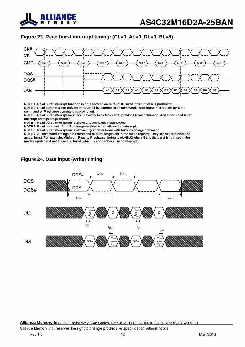
Figure 23. Read burst interrupt timing: (CL=3, AL=0, RL=3, BL=8)
CK#CK
CMD Read A NOP Read B NOP NOP NOP NOP NOP NOP NOP
A0 A1 A2 A3 B0 B1 B2 B3 B4 B5 B6 B7
DQSDQS#
DQs
NOTE 1: Read burst interrupt function is only allowed on burst of 8. Burst interrupt of 4 is prohibited.NOTE 2: Read burst of 8 can only be interrupted by another Read command. Read burst interruption by Write command or Precharge command is prohibited.NOTE 3: Read burst interrupt must occur exactly two clocks after previous Read command. Any other Read burst interrupt timings are prohibited.NOTE 4: Read burst interruption is allowed to any bank inside DRAM. NOTE 5: Read burst with Auto Precharge enabled is not allowed to interrupt.NOTE 6: Read burst interruption is allowed by another Read with Auto Precharge command.NOTE 7: All command timings are referenced to burst length set in the mode register. They are not referenced to actual burst. For example, Minimum Read to Precharge timing is AL+BL/2 where BL is the burst length set in the mode register and not the actual burst (which is shorter because of interrupt).
Figure 24. Data input (write) timing
DQS#
DQ
DQS
tDQSH
tWPRE
DQS
DM
tDQSL
tWPSL
VIL(ac)
VIH(ac)
D DVIL(dc)
VIH(dc)
D D
DMin DMin
DQS#
DMinVIH(ac)
VIL(ac)
DMinVIH(dc)
VIL(dc)
tDS tDS tDHtDH
AS4C32M16D2A-25BAN
Alliance Memory Inc. 511 Taylor Way, San Carlos, CA 94070 TEL: (650) 610-6800 FAX: (650) 620-9211
Alliance Memory Inc. reserves the right to change products or specification without noticeRev.1.5 43 Mar./2016
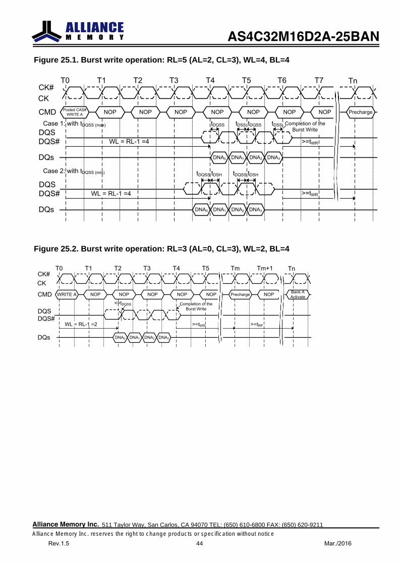
Figure 25.1. Burst write operation: RL=5 (AL=2, CL=3), WL=4, BL=4
CK#CK
tDQSS
CMDCase 1: with tDQSS (max)
>=tWR
T0 T1 T2 T3 T4 T5 T6 T7 Tn
Posted CAS#WRITE A NOP NOP NOP NOP NOP NOP NOP Precharge
tDSS tDQSS tDSS Completion of theBurst Write
WL = RL-1 =4
DNA0 DNA1 DNA2 DNA3
DQSDQS#
>=tWRWL = RL-1 =4
DNA0 DNA1 DNA2 DNA3
DQSDQS#
tDQSS tDSH tDQSS tDSHCase 2: with tDQSS (min)
DQs
DQs
Figure 25.2. Burst write operation: RL=3 (AL=0, CL=3), WL=2, BL=4
CK#CK
<=tDQSS
CMD
>=tWR
T0 T1 T2 T3 T4 T5 Tm Tm+1 Tn
WRITE A NOP NOP NOP NOP NOP Precharge NOP Bank AActivate
Completion of the Burst Write
WL = RL-1 =2
DNA0 DNA1 DNA2 DNA3
DQSDQS#
DQs
>=tRP
AS4C32M16D2A-25BAN
Alliance Memory Inc. 511 Taylor Way, San Carlos, CA 94070 TEL: (650) 610-6800 FAX: (650) 620-9211
Alliance Memory Inc. reserves the right to change products or specification without noticeRev.1.5 44 Mar./2016
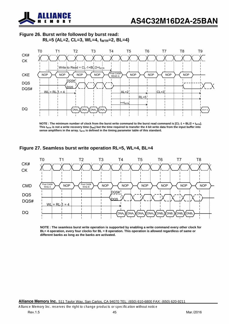
Figure 26. Burst write followed by burst read: RL=5 (AL=2, CL=3, WL=4, tWTR=2, BL=4)
CK#CK
CKE
T0 T1 T4 T5 T6 T7 T8 T9T2 T3
NOP NOP NOP NOP Post CAS#READ A NOP NOP NOP NOP
DQS
AL=2DQS#
WL = RL-1 = 4
DQS#
DQS
CL=3RL=5
>=tWTR
DNA0 DNA1 DNA2 DNA3 DOUT A0DQ
NOTE : The minimum number of clock from the burst write command to the burst read command is [CL-1 + BL/2 + tWTR].This tWTR is not a write recovery time (tWR) but the time required to transfer the 4 bit write data from the input buffer into sense amplifiers in the array. tWTR is defined in the timing parameter table of this standard.
Write to Read = CL-1+BL/2+tWTR
Figure 27. Seamless burst write operation RL=5, WL=4, BL=4
CK#CK
CMD
T0 T1 T4 T5 T6 T7 T8T2 T3
Post CAS#Write A NOP Post CAS#
Write B NOP NOP NOP NOP NOP NOP
DQSDQS#
WL = RL-1 = 4
DQS#
DQS
DNA0 DNA1 DNA2 DNA3DQ DNB0 DNB1 DNB2 DNB3
NOTE : The seamless burst write operation is supported by enabling a write command every other clock for BL= 4 operation, every four clocks for BL = 8 operation. This operation is allowed regardless of same or different banks as long as the banks are activated.
AS4C32M16D2A-25BAN
Alliance Memory Inc. 511 Taylor Way, San Carlos, CA 94070 TEL: (650) 610-6800 FAX: (650) 620-9211
Alliance Memory Inc. reserves the right to change products or specification without noticeRev.1.5 45 Mar./2016
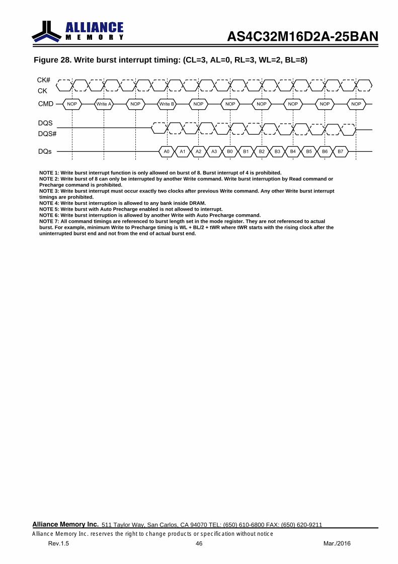
Figure 28. Write burst interrupt timing: (CL=3, AL=0, RL=3, WL=2, BL=8)
CK#CK
CMD NOP Write A NOP Write B NOP NOP NOP NOP NOP NOP
A0 A1 A2 A3 B0 B1 B2 B3 B4 B5 B6 B7
DQSDQS#
DQs
NOTE 1: Write burst interrupt function is only allowed on burst of 8. Burst interrupt of 4 is prohibited.NOTE 2: Write burst of 8 can only be interrupted by another Write command. Write burst interruption by Read command or Precharge command is prohibited.NOTE 3: Write burst interrupt must occur exactly two clocks after previous Write command. Any other Write burst interrupt timings are prohibited.NOTE 4: Write burst interruption is allowed to any bank inside DRAM.NOTE 5: Write burst with Auto Precharge enabled is not allowed to interrupt.NOTE 6: Write burst interruption is allowed by another Write with Auto Precharge command.NOTE 7: All command timings are referenced to burst length set in the mode register. They are not referenced to actual burst. For example, minimum Write to Precharge timing is WL + BL/2 + tWR where tWR starts with the rising clock after the uninterrupted burst end and not from the end of actual burst end.
AS4C32M16D2A-25BAN
Alliance Memory Inc. 511 Taylor Way, San Carlos, CA 94070 TEL: (650) 610-6800 FAX: (650) 620-9211
Alliance Memory Inc. reserves the right to change products or specification without noticeRev.1.5 46 Mar./2016
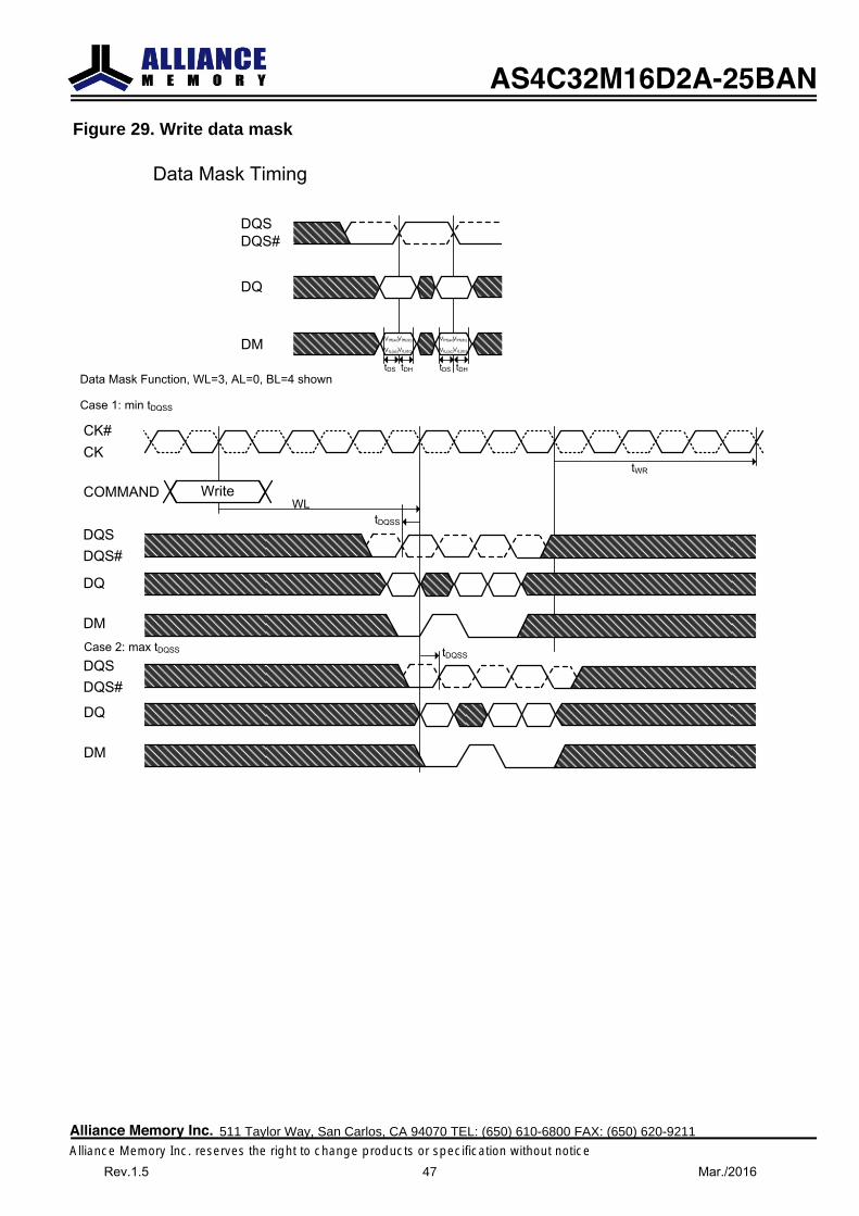
Figure 29. Write data mask
DQ
DQS
DM
DQS#
tDS
VIH(ac)VIH(dc)
VIL(ac)VIL(dc)
tDH tDS
VIH(ac)VIH(dc)
VIL(ac)VIL(dc)
tDH
CK#CK
COMMAND
DQSDQS#
DQ
Write
tWR
WLtDQSS
tDQSS
DMCase 2: max tDQSS
DQSDQS#
DQ
DM
Case 1: min tDQSS
Data Mask Function, WL=3, AL=0, BL=4 shown
Data Mask Timing
AS4C32M16D2A-25BAN
Alliance Memory Inc. 511 Taylor Way, San Carlos, CA 94070 TEL: (650) 610-6800 FAX: (650) 620-9211
Alliance Memory Inc. reserves the right to change products or specification without noticeRev.1.5 47 Mar./2016
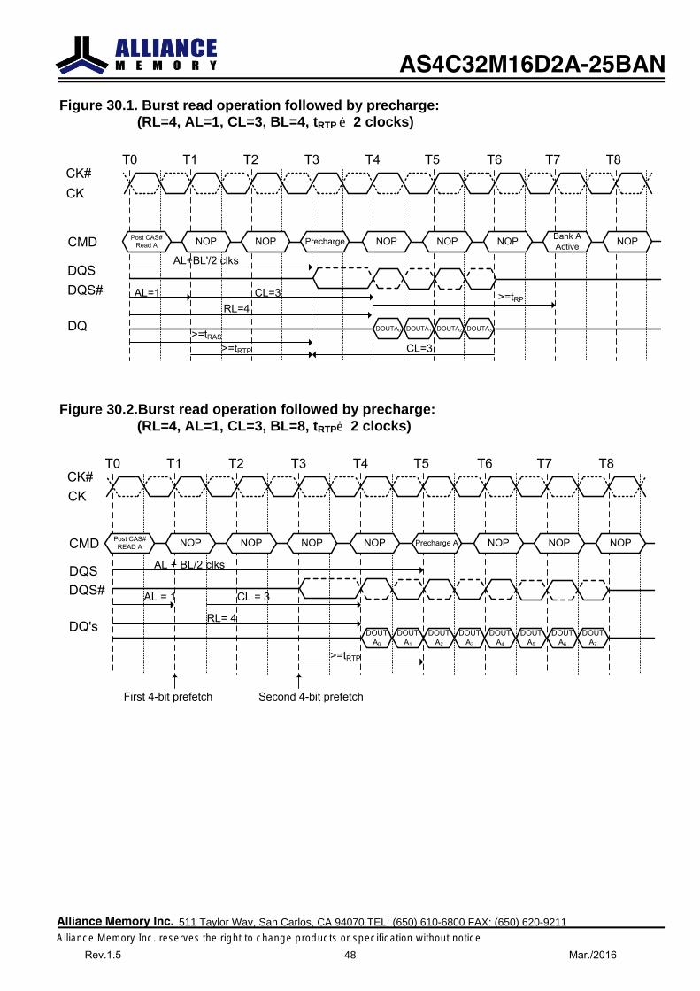
Figure 30.1. Burst read operation followed by precharge: (RL=4, AL=1, CL=3, BL=4, tRTP ≦2 clocks)
CK#CK
CMD
T0 T1 T4 T5 T6 T7 T8T2 T3
Post CAS#Read A NOP NOP Precharge NOP NOP NOP Bank A
Active NOP
DQSDQS#
AL+BL'/2 clks
DOUTA0 DOUTA1 DOUTA2 DOUTA3DQ
>=tRPAL=1 CL=3
RL=4
>=tRAS
>=tRTP CL=3
Figure 30.2.Burst read operation followed by precharge: (RL=4, AL=1, CL=3, BL=8, tRTP≦2 clocks)
CK#CK
CMD
T0 T1 T4 T5 T6 T7 T8T2 T3
Post CAS#READ A NOP NOP NOP NOP Precharge A NOP NOP NOP
DQSDQS#
RL= 4DOUT
A0
DOUT A1
DOUT A2
DOUT A3
DQ's
AL + BL/2 clks
CL = 3AL = 1
First 4-bit prefetch
>=tRTP
Second 4-bit prefetch
DOUT A4
DOUT A5
DOUT A6
DOUT A7
AS4C32M16D2A-25BAN
Alliance Memory Inc. 511 Taylor Way, San Carlos, CA 94070 TEL: (650) 610-6800 FAX: (650) 620-9211
Alliance Memory Inc. reserves the right to change products or specification without noticeRev.1.5 48 Mar./2016
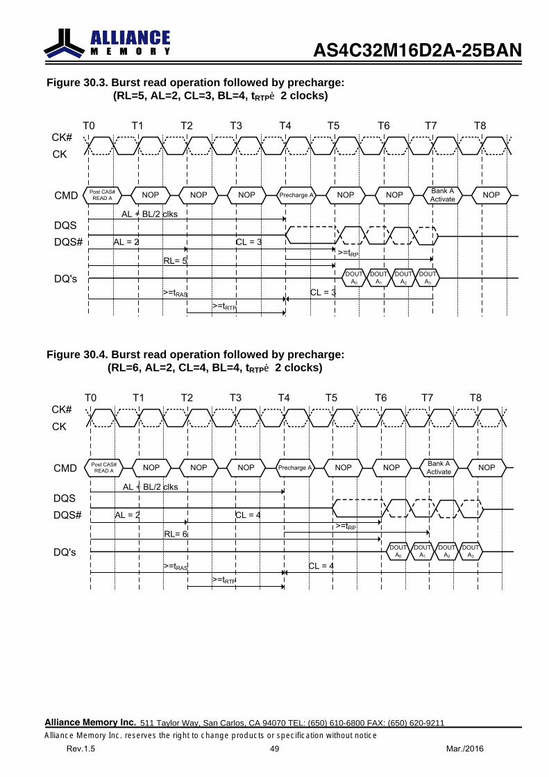
Figure 30.3. Burst read operation followed by precharge: (RL=5, AL=2, CL=3, BL=4, tRTP≦2 clocks)
CK#CK
CMD
T0 T1 T4 T5 T6 T7 T8T2 T3
Post CAS#READ A NOP NOP NOP Precharge A NOP NOP Bank A
Activate NOP
DQSDQS#
RL= 5DOUT
A0
DOUT A1
DOUT A2
DOUT A3DQ's
AL + BL/2 clks
CL = 3AL = 2
>=tRAS
>=tRP
CL = 3>=tRTP
Figure 30.4. Burst read operation followed by precharge: (RL=6, AL=2, CL=4, BL=4, tRTP≦2 clocks)
CK#CK
CMD
T0 T1 T4 T5 T6 T7 T8T2 T3
Post CAS#READ A NOP NOP NOP Precharge A NOP NOP Bank A
Activate NOP
DQSDQS#
RL= 6DOUT
A0
DOUT A1
DOUT A2
DOUT A3DQ's
AL + BL/2 clks
CL = 4AL = 2
>=tRAS
>=tRP
CL = 4>=tRTP
AS4C32M16D2A-25BAN
Alliance Memory Inc. 511 Taylor Way, San Carlos, CA 94070 TEL: (650) 610-6800 FAX: (650) 620-9211
Alliance Memory Inc. reserves the right to change products or specification without noticeRev.1.5 49 Mar./2016
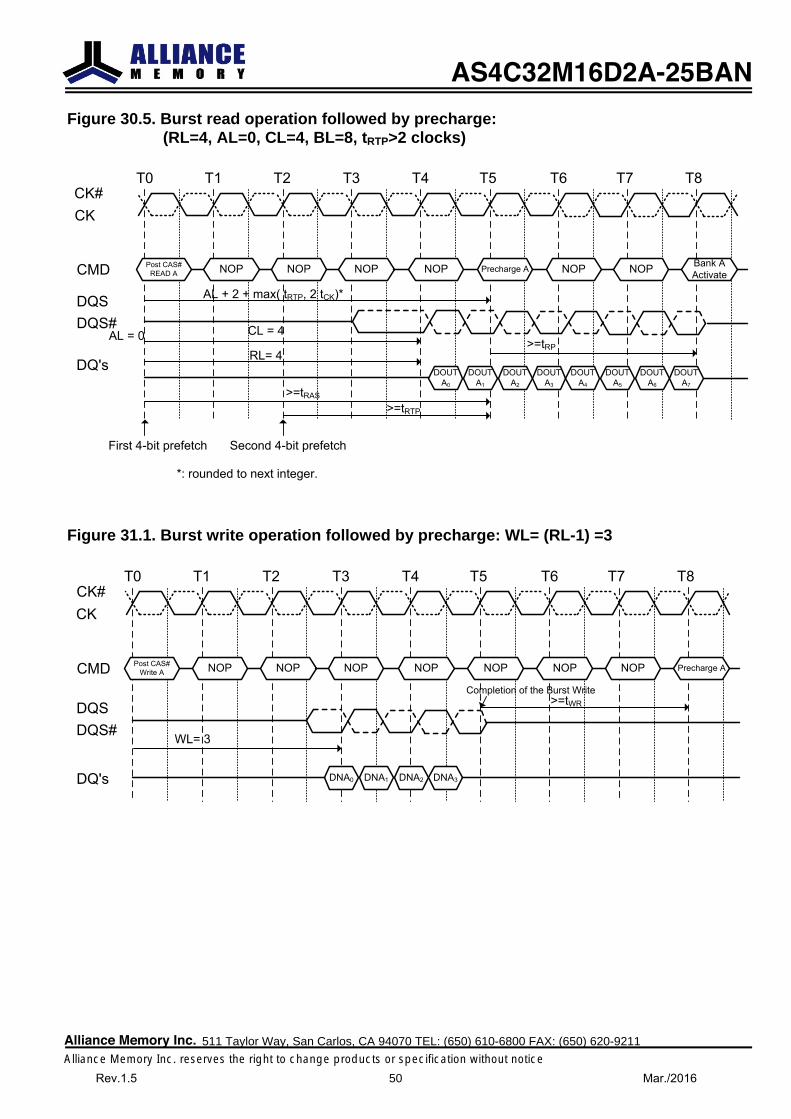
Figure 30.5. Burst read operation followed by precharge: (RL=4, AL=0, CL=4, BL=8, tRTP>2 clocks)
CK#CK
CMD
T0 T1 T4 T5 T6 T7 T8T2 T3
Post CAS#READ A NOP NOP NOP NOP Precharge A NOP NOP Bank A
Activate
DQSDQS#
RL= 4DOUT
A0
DOUT A1
DOUT A2
DOUT A3
DQ's
AL + 2 + max( tRTP, 2 tCK)*
CL = 4AL = 0
First 4-bit prefetch
>=tRTP
Second 4-bit prefetch
DOUT A4
DOUT A5
DOUT A6
DOUT A7
>=tRP
>=tRAS
*: rounded to next integer.
Figure 31.1. Burst write operation followed by precharge: WL= (RL-1) =3
CK#CK
CMD
T0 T1 T4 T5 T6 T7 T8T2 T3
Post CAS#Write A NOP NOP NOP NOP NOP NOP NOP Precharge A
DQSDQS#
DNA0 DNA1 DNA2 DNA3DQ's
>=tWR
WL= 3
Completion of the Burst Write
AS4C32M16D2A-25BAN
Alliance Memory Inc. 511 Taylor Way, San Carlos, CA 94070 TEL: (650) 610-6800 FAX: (650) 620-9211
Alliance Memory Inc. reserves the right to change products or specification without noticeRev.1.5 50 Mar./2016
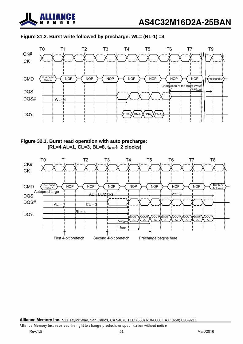
Figure 31.2. Burst write followed by precharge: WL= (RL-1) =4
CK#CK
CMD
T0 T1 T4 T5 T6 T7 T9T2 T3
Post CAS#Write A NOP NOP NOP NOP NOP NOP NOP Precharge A
DQSDQS#
DNA0 DNA1 DNA2 DNA3DQ's
>=tWR
WL= 4
Completion of the Burst Write
Figure 32.1. Burst read operation with auto precharge: (RL=4,AL=1, CL=3, BL=8, tRTP≦2 clocks)
CK#CK
CMD
T0 T1 T4 T5 T6 T7 T8T2 T3
Post CAS#READ A NOP NOP NOP NOP NOP NOP NOP Bank A
Activate
DQSDQS#
RL= 4DOUT
A0
DOUT A1
DOUT A2
DOUT A3
DQ's
AL + BL/2 clks
CL = 3AL = 1
Autoprecharge
>=tRTP
Second 4-bit prefetch
DOUT A4
DOUT A5
DOUT A6
DOUT A7
>= tRP
tRTP
Precharge begins hereFirst 4-bit prefetch
AS4C32M16D2A-25BAN
Alliance Memory Inc. 511 Taylor Way, San Carlos, CA 94070 TEL: (650) 610-6800 FAX: (650) 620-9211
Alliance Memory Inc. reserves the right to change products or specification without noticeRev.1.5 51 Mar./2016
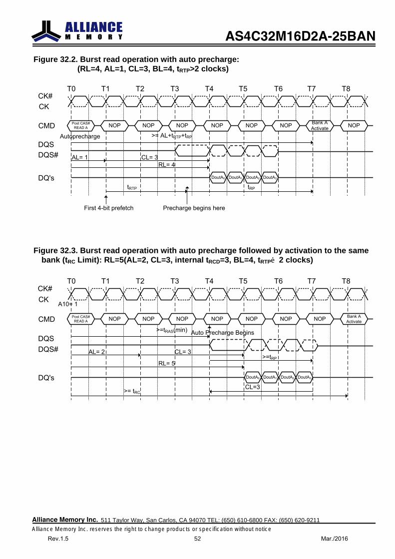
Figure 32.2. Burst read operation with auto precharge: (RL=4, AL=1, CL=3, BL=4, tRTP>2 clocks)
CK#CK
CMD
T0 T1 T4 T5 T6 T7 T8T2 T3
Post CAS#READ A NOP NOP NOP NOP NOP NOP Bank A
Activate NOP
DQSDQS#
DoutA0 DoutA1 DoutA2 DoutA3DQ's
CL= 3
Autoprecharge >= AL+tRTP+tRP
AL= 1RL= 4
tRTP tRP
First 4-bit prefetch Precharge begins here
Figure 32.3. Burst read operation with auto precharge followed by activation to the same bank (tRC Limit): RL=5(AL=2, CL=3, internal tRCD=3, BL=4, tRTP≦2 clocks)
CK#CK
CMD
T0 T1 T4 T5 T6 T7 T8T2 T3
Post CAS#READ A NOP NOP NOP NOP NOP NOP NOP Bank A
Activate
DQSDQS#
DoutA0 DoutA1 DoutA2 DoutA3DQ's
CL= 3
>=tRAS(min)
AL= 2
RL= 5
>= tRCCL=3
A10= 1
Auto Precharge Begins
>=tRP
AS4C32M16D2A-25BAN
Alliance Memory Inc. 511 Taylor Way, San Carlos, CA 94070 TEL: (650) 610-6800 FAX: (650) 620-9211
Alliance Memory Inc. reserves the right to change products or specification without noticeRev.1.5 52 Mar./2016
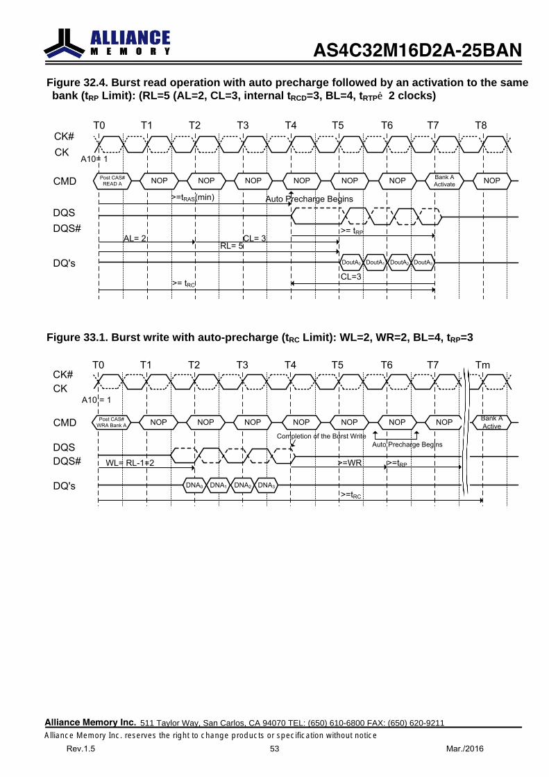
Figure 32.4. Burst read operation with auto precharge followed by an activation to the same bank (tRP Limit): (RL=5 (AL=2, CL=3, internal tRCD=3, BL=4, tRTP≦2 clocks)
CK#CK
CMD
T0 T1 T4 T5 T6 T7 T8T2 T3
Post CAS#READ A NOP NOP NOP NOP NOP NOP Bank A
Activate NOP
DQSDQS#
DoutA0 DoutA1 DoutA2 DoutA3DQ's
CL= 3
>=tRAS(min)
AL= 2RL= 5
>= tRCCL=3
A10= 1
Auto Precharge Begins
>= tRP
Figure 33.1. Burst write with auto-precharge (tRC Limit): WL=2, WR=2, BL=4, tRP=3
CK#CK
CMD
T0 T1 T4 T5 T6 T7 TmT2 T3
Post CAS#WRA Bank A NOP NOP NOP NOP NOP NOP NOP Bank A
Active
DQSDQS#
DNA0 DNA1 DNA2 DNA3DQ's
Auto Precharge Begins
WL= RL-1=2
Completion of the Burst Write
A10 = 1
>=WR >=tRP
>=tRC
AS4C32M16D2A-25BAN
Alliance Memory Inc. 511 Taylor Way, San Carlos, CA 94070 TEL: (650) 610-6800 FAX: (650) 620-9211
Alliance Memory Inc. reserves the right to change products or specification without noticeRev.1.5 53 Mar./2016
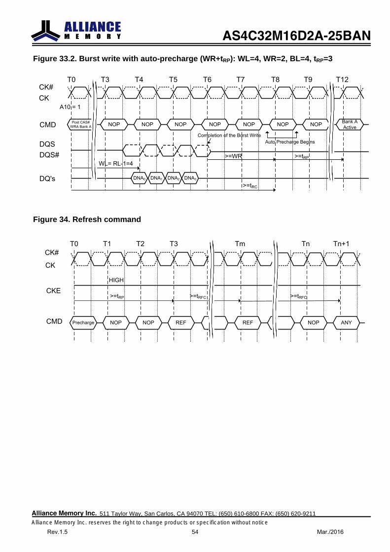
Figure 33.2. Burst write with auto-precharge (WR+tRP): WL=4, WR=2, BL=4, tRP=3
CK#CK
CMD
T0 T3 T6 T7 T8 T9 T12T4 T5
Post CAS#WRA Bank A NOP NOP NOP NOP NOP NOP NOP Bank A
Active
DQSDQS#
DNA0 DNA1 DNA2 DNA3DQ's
Auto Precharge Begins
WL= RL-1=4
Completion of the Burst Write
A10 = 1
>=WR >=tRP
>=tRC
Figure 34. Refresh command
CK#
CK
CKE
T0 T1 Tm Tn Tn+1T2 T3
Precharge NOP NOP REF REF NOP ANYCMD
HIGH
>=tRP >=tRFC >=tRFC
AS4C32M16D2A-25BAN
Alliance Memory Inc. 511 Taylor Way, San Carlos, CA 94070 TEL: (650) 610-6800 FAX: (650) 620-9211
Alliance Memory Inc. reserves the right to change products or specification without noticeRev.1.5 54 Mar./2016
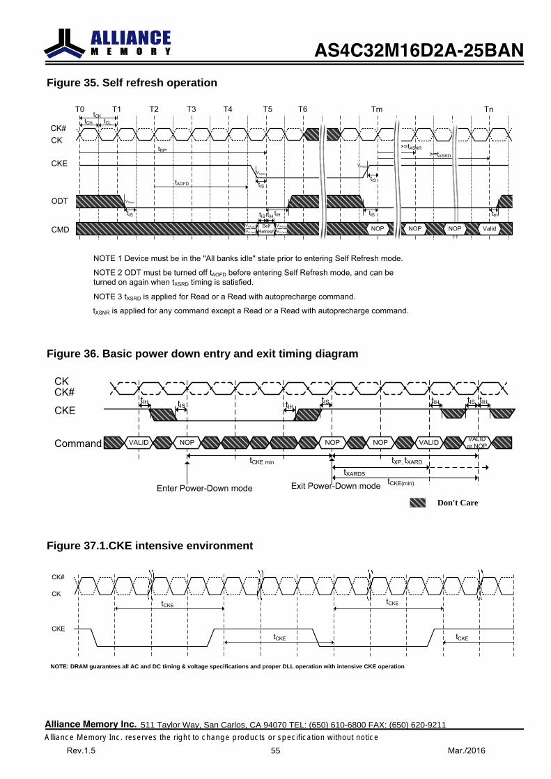
Figure 35. Self refresh operation
CK#CK
CKE
T0 T1 T5 TmT2 T3
CMD
>=tXSNRtRP*
tCH tCL
tCK T4 T6 Tn
>=tXSRD
tIS
VIL(ac)
VIH(ac)
tIS
NOPSelfRefresh
ODT
tAOFD
tIS
VIL(ac)
tIH tIS tIHtIS tIH
VIL(dc)VIL(ac)
VIH(ac) VIH(dc) NOP NOP Valid
NOTE 1 Device must be in the "All banks idle" state prior to entering Self Refresh mode.
NOTE 2 ODT must be turned off tAOFD before entering Self Refresh mode, and can be turned on again when tXSRD timing is satisfied.
NOTE 3 tXSRD is applied for Read or a Read with autoprecharge command.
tXSNR is applied for any command except a Read or a Read with autoprecharge command.
Figure 36. Basic power down entry and exit timing diagram
CK#CK
Command
CKE
VALID
tIH
tCKE min
tIH tIH tIHtIS tIS tIS
NOP NOP NOP VALID VALIDor NOP
tXP, tXARD
tXARDStCKE(min)Exit Power-Down mode
Don't Care
Enter Power-Down mode
Figure 37.1.CKE intensive environment
CK#
CKE
tCKE
NOTE: DRAM guarantees all AC and DC timing & voltage specifications and proper DLL operation with intensive CKE operation
CKtCKE
tCKEtCKE
AS4C32M16D2A-25BAN
Alliance Memory Inc. 511 Taylor Way, San Carlos, CA 94070 TEL: (650) 610-6800 FAX: (650) 620-9211
Alliance Memory Inc. reserves the right to change products or specification without noticeRev.1.5 55 Mar./2016
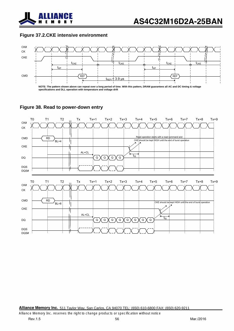
Figure 37.2.CKE intensive environment
CK#
CKE
tCKE
NOTE: The pattern shown above can repeat over a long period of time. With this pattern, DRAM guarantees all AC and DC timing & voltage specifications and DLL operation with temperature and voltage drift
CK
tCKE tCKEtCKE
tXPtXP
tREFI = 3.9 µsREF REFCMD
Figure 38. Read to power-down entry
CK#
CMDBL=4
T0 T2 Tx Tx+1 Tx+2 Tx+3 Tx+4 Tx+5 Tx+6 Tx+7T1 Tx+8 Tx+9
RD
Q
AL+CL
Read operation starts with a read command and
DQS
CKE
CK
DQS#
CKE should be kept HIGH until the end of burst operation
tISQ Q QDQ
CK#
CMDBL=8
T0 T2 Tx Tx+1 Tx+2 Tx+3 Tx+4 Tx+5 Tx+6 Tx+7T1 Tx+8 Tx+9
RD
Q
AL+CL
DQS
CKE
CK
DQS#
CKE should be kept HIGH until the end of burst operation
tISQ Q QDQ Q Q Q Q
AS4C32M16D2A-25BAN
Alliance Memory Inc. 511 Taylor Way, San Carlos, CA 94070 TEL: (650) 610-6800 FAX: (650) 620-9211
Alliance Memory Inc. reserves the right to change products or specification without noticeRev.1.5 56 Mar./2016
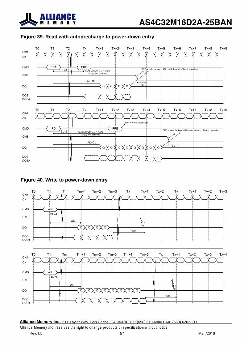
Figure 39. Read with autoprecharge to power-down entry
CK#
CMDBL=4
T0 T2 Tx Tx+1 Tx+2 Tx+3 Tx+4 Tx+5 Tx+6 Tx+7T1 Tx+8 Tx+9
RDA
Q
AL+CL
DQS
CKE
CK
DQS#
CKE should be kept HIGH until the end of burst operation
tISQ Q QDQ
CK#
CMDBL=8
T0 T2 Tx Tx+1 Tx+2 Tx+3 Tx+4 Tx+5 Tx+6 Tx+7T1 Tx+8 Tx+9
RD
Q
AL+CL
DQS
CKE
CK
DQS#
CKE should be kept HIGH until the end of burst operation
tISQ Q QDQ Q Q Q Q
PREAL+BL/2 with tRTP = 7.5ns
& tRAS min satisfied
PRE
Start internal precharge
AL+BL/2 with tRTP = 7.5ns & tRAS min satisfied
Figure 40. Write to power-down entry
CK#
CMD
BL=4
T0 Tm Tm+1 Tm+2 Tm+3 Tx Tx+1 Tx+2 Ty Ty+1T1 Ty+2 Ty+3
WR
Q
WL
DQS
CKE
CK
DQS#
tISQ Q QDQ
CK#
CMDBL=8
T0 Tm Tm+1 Tm+2 Tm+3 Tm+4 Tm+5 Tx Tx+1 Tx+2T1 Tx+3 Tx+4
WR
Q
WL
DQS
CKE
CK
DQS#
Q Q QDQ Q Q Q Q
tWTR
tIS
tWTR
AS4C32M16D2A-25BAN
Alliance Memory Inc. 511 Taylor Way, San Carlos, CA 94070 TEL: (650) 610-6800 FAX: (650) 620-9211
Alliance Memory Inc. reserves the right to change products or specification without noticeRev.1.5 57 Mar./2016
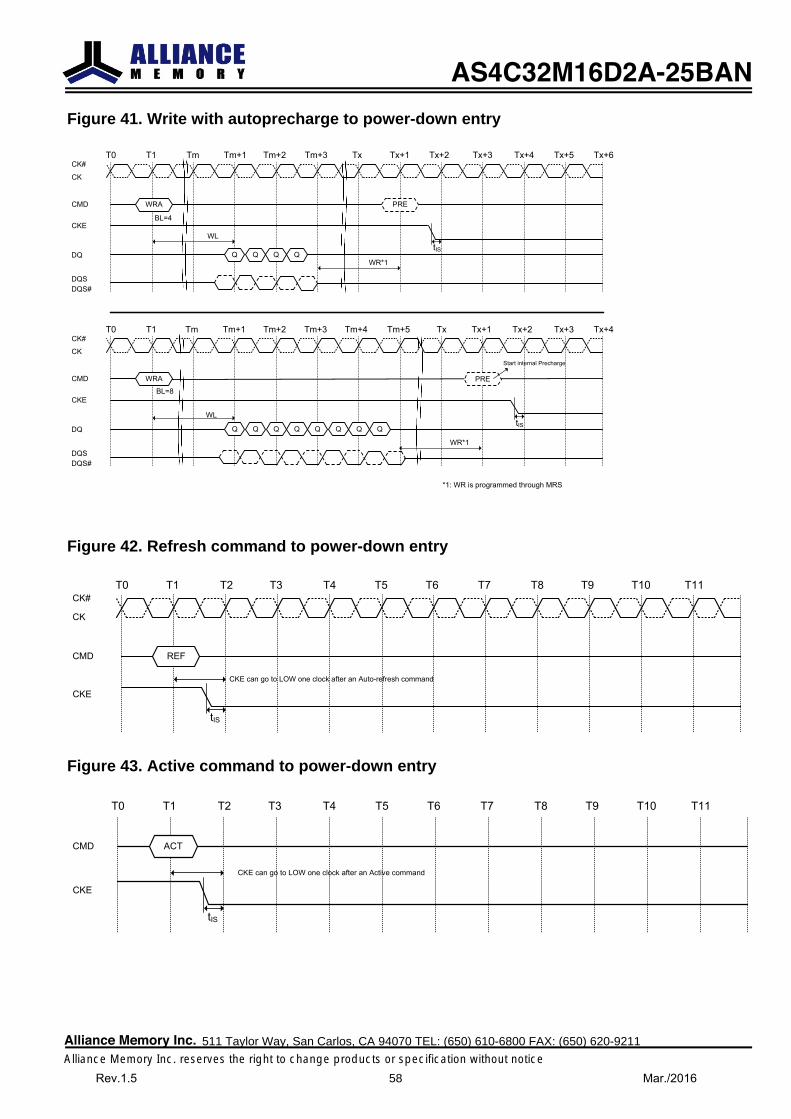
Figure 41. Write with autoprecharge to power-down entry
CK#
CMD
BL=4
T0 Tm Tm+1 Tm+2 Tm+3 Tx Tx+1 Tx+2 Tx+3 Tx+4T1 Tx+5 Tx+6
WRA
Q
WL
DQS
CKE
CK
DQS#
tISQ Q QDQ
CK#
CMD
BL=8
T0 Tm Tm+1 Tm+2 Tm+3 Tm+4 Tm+5 Tx Tx+1 Tx+2T1 Tx+3 Tx+4
WRA
Q
WL
DQS
CKE
CK
DQS#
Q Q QDQ Q Q Q Q
WR*1
tIS
PRE
WR*1
PRE
Start internal Precharge
*1: WR is programmed through MRS
Figure 42. Refresh command to power-down entry
CK#
CMD
T0 T2 T3 T4 T5 T6 T7 T8 T9 T10T1
REF
CKE
CK
tIS
T11
CKE can go to LOW one clock after an Auto-refresh command
Figure 43. Active command to power-down entry
CMD
T0 T2 T3 T4 T5 T6 T7 T8 T9 T10T1
ACT
CKE
tIS
T11
CKE can go to LOW one clock after an Active command
AS4C32M16D2A-25BAN
Alliance Memory Inc. 511 Taylor Way, San Carlos, CA 94070 TEL: (650) 610-6800 FAX: (650) 620-9211
Alliance Memory Inc. reserves the right to change products or specification without noticeRev.1.5 58 Mar./2016
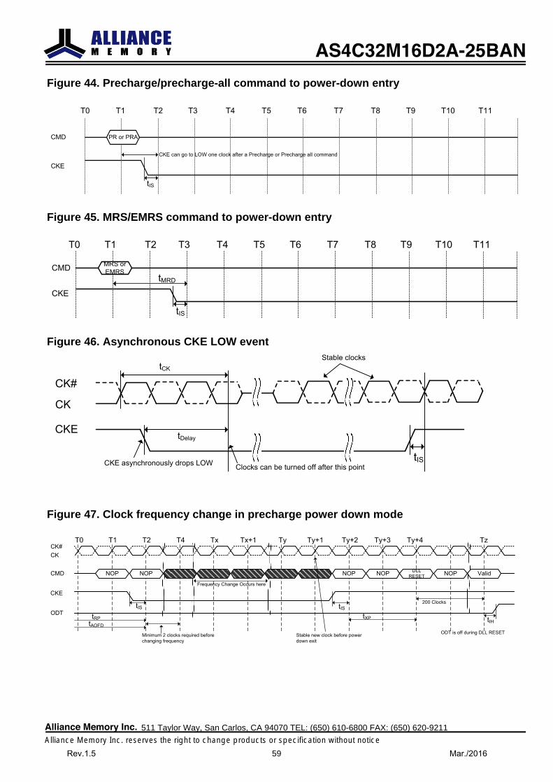
Figure 44. Precharge/precharge-all command to power-down entry
CMD
T0 T2 T3 T4 T5 T6 T7 T8 T9 T10T1
PR or PRA
CKE
tIS
T11
CKE can go to LOW one clock after a Precharge or Precharge all command
Figure 45. MRS/EMRS command to power-down entry
CMD
T0 T2 T3 T4 T5 T6 T7 T8 T9 T10T1
MRS or EMRS
CKE
tIS
T11
tMRD
Figure 46. Asynchronous CKE LOW event
CK#
CK
CKE
tCK
tDelay
CKE asynchronously drops LOW Clocks can be turned off after this pointtIS
Stable clocks
Figure 47. Clock frequency change in precharge power down mode
CK#
CMD
T0 T2 T4 Tx Tx+1 Ty Ty+1 Ty+2 Ty+3 Ty+4T1 Tz
Frequency Change Occurs here
tRP
CKE
ODT
CK
NOP NOP NOP NOP DLLRESET NOP Valid
200 Clocks
tAOFD
Minimum 2 clocks required before changing frequency
Stable new clock before power down exit
tXP
tIS tIS
tIHODT is off during DLL RESET
AS4C32M16D2A-25BAN
Alliance Memory Inc. 511 Taylor Way, San Carlos, CA 94070 TEL: (650) 610-6800 FAX: (650) 620-9211
Alliance Memory Inc. reserves the right to change products or specification without noticeRev.1.5 59 Mar./2016
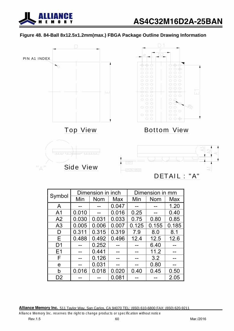
Figure 48. 84-Ball 8x12.5x1.2mm(max.) FBGA Package Outline Drawing Information
Top V iew Bottom V iew
S ide V iew
PIN A1 IN D EX
D ETA IL : "A "
Symbol Dimension in inch Dimension in mm Min Nom Max Min Nom Max
A -- -- 0.047 -- -- 1.20 A1 0.010 -- 0.016 0.25 -- 0.40 A2 0.030 0.031 0.033 0.75 0.80 0.85 A3 0.005 0.006 0.007 0.125 0.155 0.185 D 0.311 0.315 0.319 7.9 8.0 8.1 E 0.488 0.492 0.496 12.4 12.5 12.6
D1 -- 0.252 -- -- 6.40 -- E1 -- 0.441 -- -- 11.2 -- F -- 0.126 -- -- 3.2 -- e -- 0.031 -- -- 0.80 -- b 0.016 0.018 0.020 0.40 0.45 0.50
D2 -- -- 0.081 -- -- 2.05
AS4C32M16D2A-25BAN
Alliance Memory Inc. 511 Taylor Way, San Carlos, CA 94070 TEL: (650) 610-6800 FAX: (650) 620-9211
Alliance Memory Inc. reserves the right to change products or specification without noticeRev.1.5 60 Mar./2016
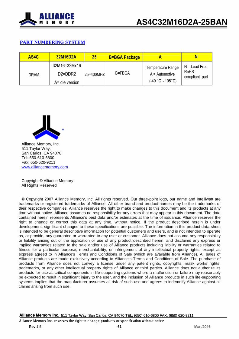
PART NUMBERING SYSTEM
AS4C 25 B=BGA Package A N
DRAM
32M16=32Mx16D2=DDR2
A= die version25=400MHZ B=FBGA
Temperature Range
A = Automotive (-40 °C~105°C)
N = Lead Free RoHS compliant part
32M16D2A
Alliance Memory Inc. 511 Taylor Way, San Carlos, CA 94070 TEL: (650) 610-6800 FAX: (650) 620-9211
Alliance Memory Inc. reserves the right to change products or specification without noticeRev. 1.2 61
Alliance Memory Inc. 511 Taylor Way, San Carlos, CA 94070 TEL: (650) 610-6800 FAX: (650) 620-9211
Alliance Memory Inc. reserves the right to change products or specification without noticeRev.1.5 61 Mar./2016
AS4C32M16D2A-25BAN
Alliance Memory, Inc. 511 Taylor Way, San Carlos, CA 94070 Tel: 650-610-6800 Fax: 650-620-9211 www.alliancememory.com
Copyright © Alliance Memory All Rights Reserved
© Copyright 2007 Alliance Memory, Inc. All rights reserved. Our three-point logo, our name and Intelliwatt are trademarks or registered trademarks of Alliance. All other brand and product names may be the trademarks of their respective companies. Alliance reserves the right to make changes to this document and its products at any time without notice. Alliance assumes no responsibility for any errors that may appear in this document. The data contained herein represents Alliance's best data and/or estimates at the time of issuance. Alliance reserves the right to change or correct this data at any time, without notice. If the product described herein is under development, significant changes to these specifications are possible. The information in this product data sheet is intended to be general descriptive information for potential customers and users, and is not intended to operate as, or provide, any guarantee or warrantee to any user or customer. Alliance does not assume any responsibility or liability arising out of the application or use of any product described herein, and disclaims any express or implied warranties related to the sale and/or use of Alliance products including liability or warranties related to fitness for a particular purpose, merchantability, or infringement of any intellectual property rights, except as express agreed to in Alliance's Terms and Conditions of Sale (which are available from Alliance). All sales of Alliance products are made exclusively according to Alliance's Terms and Conditions of Sale. The purchase of products from Alliance does not convey a license under any patent rights, copyrights; mask works rights, trademarks, or any other intellectual property rights of Alliance or third parties. Alliance does not authorize its products for use as critical components in life-supporting systems where a malfunction or failure may reasonably be expected to result in significant injury to the user, and the inclusion of Alliance products in such life-supporting systems implies that the manufacturer assumes all risk of such use and agrees to indemnify Alliance against all claims arising from such use.