Embed Size (px)
Citation preview


*326348A-01*326348A-01 Dec14
PRINTED IN HUNGARY
326348A-01
Introduction to
Communication Systems
Lab Based Learning with NI USRP
and LabVIEW Communications
Student Lab Manual
Bruce A. Black
2
Worldwide Technical Support and Product Information ni.com National Instruments Corporate Headquarters 11500 N Mopac Expwy Austin, Texas 78759-3504 USA Tel: 512 683 0100 Worldwide Offices Visit ni.com/global for the latest contact information. Andean and Caribbean +58 212 503-5310, Argentina 0800 666 0037, Australia 1800 300 800, Austria 43 662 45 79 90 0, Belgium 32 0 2 757 00 20, Brazil 55 11 3262 3599, Canada 800 433 3488, Chile 800 532 951, China 86 21 5050 9800, Czech Republic/Slovakia 420 224 235 774, Denmark 45 45 76 26 00, Finland 358 0 9 725 725 11, France 33 0 1 48 14 24 24, Germany 49 89 741 31 30, Hungary 36 23 501 580, India 1 800 425 7070, Ireland 353 0 1867 4374, Israel 972 3 6393737, Italy 39 02 413091, Japan 81 3 5472 2970, Korea 82 02 3451 3400, Lebanon 961 0 1 33 28 28, Malaysia 1800 887710, Mexico 01 800 010 0793, Netherlands 31 0 348 433 466, New Zealand 0800 553 322, Norway 47 0 66 90 76 60, Poland 48 22 3390150, Portugal 351 210 311 210, Russia 7 495 783 68 51, Singapore 1800 226 5886, Slovenia/Croatia, Bosnia/Herzegovina, Serbia/Montenegro, Macedonia 386 3 425 42 00, South Africa 27 0 11 805 8197, Spain 34 91 640 0085, Sweden 46 0 8 587 895 00, Switzerland 41 56 200 51 51, Taiwan 886 2 2377 2222, Thailand 662 278 6777, Turkey 90 212 279 3031, U.K. 44 0 1635 523545, Uruguay 0004 055 114 © 2014 National Instruments. All rights reserved. Important Information Warranty The media on which you receive National Instruments software are warranted not to fail to execute programming instructions, due to defects in materials and workmanship, for a period of 90 days from date of shipment, as evidenced by receipts or other documentation. National Instruments will, at its option, repair or replace software media that do not execute programming instructions if National Instruments receives notice of such defects during the warranty period. National Instruments does not warrant that the operation of the software shall be uninterrupted or error free. A Return Material Authorization (RMA) number must be obtained from the factory and clearly marked on the outside of the package before any equipment will be accepted for warranty work. National Instruments will pay the shipping costs of returning to the owner parts, which are covered by warranty. National Instruments believes that the information in this document is accurate. The document has been carefully reviewed for technical accuracy. In the event that technical or typographical errors exist, National Instruments reserves the right to make changes to subsequent editions of this document without prior notice to holders of this edition. The reader should consult National Instruments if errors are suspected. In no event shall National Instruments be liable for any damages arising out of or related to this document or the information contained in it. EXCEPT AS SPECIFIED HEREIN, NATIONAL INSTRUMENTS MAKES NO WARRANTIES, EXPRESS OR IMPLIED, AND SPECIFICALLY DISCLAIMS ANY WARRANTY OF MERCHANTABILITY OR FITNESS FOR A PARTICULAR PURPOSE. CUSTOMER’S RIGHT TO RECOVER DAMAGES CAUSED BY FAULT OR NEGLIGENCE ON THE PART OF NATIONAL INSTRUMENTS SHALL BE LIMITED TO THE AMOUNT THERETOFORE PAID BY THE CUSTOMER. NATIONAL INSTRUMENTS WILL NOT BE LIABLE FOR DAMAGES RESULTING FROM LOSS OF DATA, PROFITS, USE OF PRODUCTS, OR INCIDENTAL OR CONSEQUENTIAL DAMAGES, EVEN IF ADVISED OF THE POSSIBILITY THEREOF. This limitation of the liability of National Instruments will apply regardless of the form of action, whether in contract or tort, including negligence. Any action against National Instruments must be brought within one year after the cause of action accrues. National Instruments shall not be liable for any delay in performance due to causes beyond its reasonable control. The warranty provided herein does not cover damages, defects, malfunctions, or service failures caused by owner’s failure to follow the National Instruments installation, operation, or maintenance instructions; owner’s modification of the product; owner’s abuse, misuse, or negligent acts; and power failure or surges, fire, flood, accident, actions of third parties, or other events outside reasonable control.

3
Copyright Under the copyright laws, this publication may not be reproduced or transmitted in any form, electronic or mechanical, including photocopying, recording, storing in an information retrieval system, or translating, in whole or in part, without the prior written consent of National Instruments Corporation. National Instruments respects the intellectual property of others, and we ask our users to do the same. NI software is protected by copyright and other intellectual property laws. Where NI software may be used to reproduce software or other materials belonging to others, you may use NI software only to reproduce materials that you may reproduce in accordance with the terms of any applicable license or other legal restriction. Trademarks LabVIEW, National Instruments, NI, ni.com, and USRP are trademarks of National Instruments. Refer to the Terms of Use section on ni.com/legal for more information about National Instruments trademarks. Other product and company names mentioned herein are trademarks or trade names of their respective companies. Patents For patents covering National Instruments products, refer to ni.com/patents. Some portions of this product are protected under United States Patent No. 6,560,572. WARNING REGARDING USE OF NATIONAL INSTRUMENTS PRODUCTS (1) NATIONAL INSTRUMENTS PRODUCTS ARE NOT DESIGNED WITH COMPONENTS AND TESTING FOR A LEVEL OF RELIABILITY SUITABLE FOR USE IN OR IN CONNECTION WITH SURGICAL IMPLANTS OR AS CRITICAL COMPONENTS IN ANY LIFE SUPPORT SYSTEMS WHOSE FAILURE TO PERFORM CAN REASONABLY BE EXPECTED TO CAUSE SIGNIFICANT INJURY TO A HUMAN. (2) IN ANY APPLICATION, INCLUDING THE ABOVE, RELIABILITY OF OPERATION OF THE SOFTWARE PRODUCTS CAN BE IMPAIRED BY ADVERSE FACTORS, INCLUDING BUT NOT LIMITED TO FLUCTUATIONS IN ELECTRICAL POWER SUPPLY, COMPUTER HARDWARE MALFUNCTIONS, COMPUTER OPERATING SYSTEM SOFTWARE FITNESS, FITNESS OF COMPILERS AND DEVELOPMENT SOFTWARE USED TO DEVELOP AN APPLICATION, INSTALLATION ERRORS, SOFTWARE AND HARDWARE COMPATIBILITY PROBLEMS, MALFUNCTIONS OR FAILURES OF ELECTRONIC MONITORING OR CONTROL DEVICES, TRANSIENT FAILURES OF ELECTRONIC SYSTEMS (HARDWARE AND/OR SOFTWARE), UNANTICIPATED USES OR MISUSES, OR ERRORS ON THE PART OF THE USER OR APPLICATIONS DESIGNER (ADVERSE FACTORS SUCH AS THESE ARE HEREAFTER COLLECTIVELY TERMED “SYSTEM FAILURES”). ANY APPLICATION WHERE A SYSTEM FAILURE WOULD CREATE A RISK OF HARM TO PROPERTY OR PERSONS (INCLUDING THE RISK OF BODILY INJURY AND DEATH) SHOULD NOT BE RELIANT SOLELY UPON ONE FORM OF ELECTRONIC SYSTEM DUE TO THE RISK OF SYSTEM FAILURE. TO AVOID DAMAGE, INJURY, OR DEATH, THE USER OR APPLICATION DESIGNER MUST TAKE REASONABLY PRUDENT STEPS TO PROTECT AGAINST SYSTEM FAILURES, INCLUDING BUT NOT LIMITED TO BACK-UP OR SHUT DOWN MECHANISMS. BECAUSE EACH END-USER SYSTEM IS CUSTOMIZED AND DIFFERS FROM NATIONAL INSTRUMENTS' TESTING PLATFORMS AND BECAUSE A USER OR APPLICATION DESIGNER MAY USE NATIONAL INSTRUMENTS PRODUCTS IN COMBINATION WITH OTHER PRODUCTS IN A MANNER NOT EVALUATED OR CONTEMPLATED BY NATIONAL INSTRUMENTS, THE USER OR APPLICATION DESIGNER IS ULTIMATELY RESPONSIBLE FOR VERIFYING AND VALIDATING THE SUITABILITY OF NATIONAL INSTRUMENTS PRODUCTS WHENEVER NATIONAL INSTRUMENTS PRODUCTS ARE INCORPORATED IN A SYSTEM OR APPLICATION, INCLUDING, WITHOUT LIMITATION, THE APPROPRIATE DESIGN, PROCESS AND SAFETY LEVEL OF SUCH SYSTEM OR APPLICATION.
4
Table of Contents Preface ..................................................................................................................................... 5
Introduction to the USRP .......................................................................................................... 7
Amplitude Modulation ............................................................................................................ 15
Frequency-Division Multiplexing .............................................................................................. 29
Image Rejection ...................................................................................................................... 37
Double-Sideband Suppressed-Carrier ....................................................................................... 49
Frequency Modulation ............................................................................................................ 59
Amplitude-Shift Keying ........................................................................................................... 69
Frequency-Shift Keying ........................................................................................................... 85
Binary Phase-Shift Keying (BPSK) .......................................................................................... 101
The Eye Diagram .................................................................................................................. 119
Equalization ......................................................................................................................... 129
Quadrature Phase-Shift Keying ............................................................................................. 143

5
Preface The twelve lab exercises presented in this package are intended to accompany an introductory
course in communication systems offered at the junior or senior level in an electrical or computer
engineering program. The lab exercises use the NI USRP software defined radio platform; no
additional laboratory equipment is needed, other than a computer to run LabVIEW
Communications and to interface with the USRP. The USRP transceivers are operated in loopback
mode with a coaxial cable and attenuator connecting the transmitter to the receiver.
The first lab exercise is an introduction to the USRP. This exercise is brief to allow time for an
instructor to add an introduction to LabVIEW Communications for students who are unfamiliar with
the programming environment. Labs two through six introduce various aspects of analog
communication, including AM, frequency-division multiplexing, image rejection, double-sideband
suppressed-carrier modulation, and FM. Labs six through twelve introduce various digital signaling
techniques, including amplitude-shift keying, frequency-shift keying, binary phase-shift keying, the
eye diagram, equalization, and quadrature phase-shift keying. Introducing analog modulation as a
lead-in to digital techniques follows the approach used in most current communication systems
textbooks.
These lab exercises are intended for students who have a basic background in signals and systems,
and are beginning study of communication systems. Some prior experience with LabVIEW would
be helpful, but this can be provided by the instructor at the beginning of the lab sequence. These
lab exercises are intended to accompany a traditional communication systems course; they are not
intended for self study. Each of the lab project descriptions begins with a background discussion,
but these have been kept brief, and it is assumed that the accompanying course will provide
detailed background as well as context for the lab projects.
Each of the lab projects after the introductory lab includes a prelab assignment, an in-lab exercise,
and a lab report. Generally, each prelab assignment involves creating LabVIEW “virtual
instruments” (VI’s) to implement a transmitter and a receiver using a specified modulation method.
Templates are provided to help students structure their programs and to assist in interfacing to the
USRP. During the laboratory sessions, students will try out their virtual instruments on the USRP’s,
and correct errors. Some of the lab projects ask students to explore the effects of varying
modulation parameters, other projects involve creating additional VI’s to explore alternative
methods such as differential phase-shift keying. Students are expected to submit their working
programs and functions accompanied by documentation and measurement results after
completing each lab exercise.
The twelve lab projects should be sufficient to support a one-semester course. For a one-quarter
course spanning ten weeks, Labs 3 and 4 can be omitted without compromising continuity.

6
The USRP provides a powerful and flexible platform for learning about communication systems.
They also provide a significant opportunity for advanced experimentation, beyond the scope of the
lab projects presented here.
In order to complete labs 2 - 12, you will need to download the corresponding LabVIEW program
files. Download these files from http://www.ni.com/white-paper/52344/en/ and unzip the files to
a convenient location. You will access them as instructed by each lab.
Instructors, please visit www.ntspress.com/publications/usrp-labs/ for more information.

7
L A B 1
Introduction to the USRP
8
1.1 Objective The purpose of this introductory laboratory exercise is to ensure that students have a working
installation of LabVIEW Communications on their computers and know how to connect to the USRP
software defined radio.
1.2 Background The Wireless Innovation Forum defines Software Defined Radio (SDR) as:
“Radio in which some or all of the physical layer functions are software defined.” 1
SDR refers to the technology wherein software modules running on a generic hardware platform
are used to implement radio functions. By combining the NI USRP hardware with LabVIEW
software you can create a flexible and functional SDR platform for rapid prototyping of wireless
signals including physical layer design, record and playback, signal intelligence, algorithm
validation, and more.
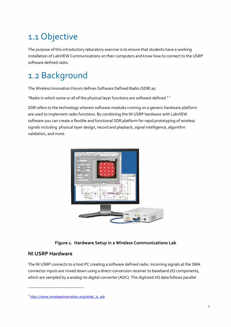
Figure 1. Hardware Setup in a Wireless Communications Lab
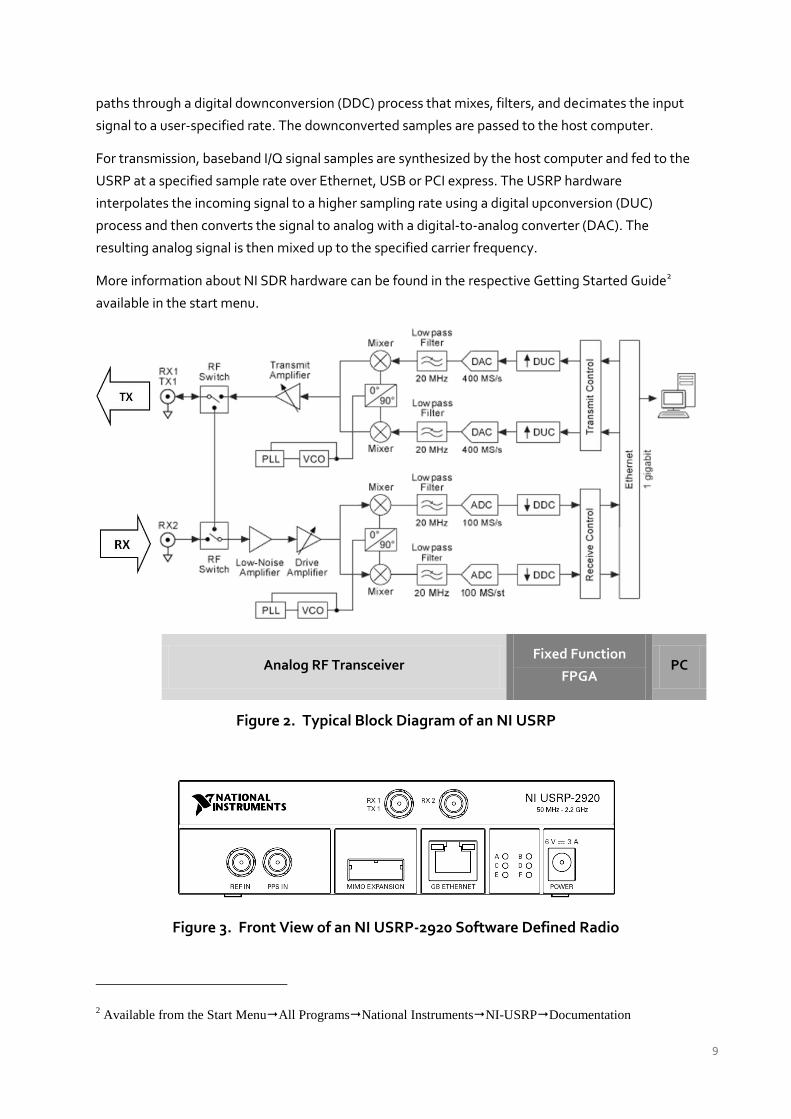
NI USRP Hardware The NI USRP connects to a host PC creating a software defined radio. Incoming signals at the SMA
connector inputs are mixed down using a direct-conversion receiver to baseband I/Q components,
which are sampled by a analog-to-digital converter (ADC). The digitized I/Q data follows parallel
1 http://www.wirelessinnovation.org/what_is_sdr
9
paths through a digital downconversion (DDC) process that mixes, filters, and decimates the input
signal to a user-specified rate. The downconverted samples are passed to the host computer.
For transmission, baseband I/Q signal samples are synthesized by the host computer and fed to the
USRP at a specified sample rate over Ethernet, USB or PCI express. The USRP hardware
interpolates the incoming signal to a higher sampling rate using a digital upconversion (DUC)
process and then converts the signal to analog with a digital-to-analog converter (DAC). The
resulting analog signal is then mixed up to the specified carrier frequency.
More information about NI SDR hardware can be found in the respective Getting Started Guide2
available in the start menu.
Analog RF Transceiver Fixed Function
FPGA PC
Figure 2. Typical Block Diagram of an NI USRP
Figure 3. Front View of an NI USRP-2920 Software Defined Radio
2 Available from the Start MenuAll ProgramsNational InstrumentsNI-USRPDocumentation
10
NI LabVIEW Communications System Design Software
LabVIEW is a graphical programming language developed by National Instruments. The basic
building block of LabVIEW is the virtual instrument (VI). Conceptually, a VI is analogous to a
procedure or function in conventional programming languages. Each VI consists of a block diagram
and a front panel. The block diagram describes the functionality of the VI, while the front panel is a
top level interface to the VI. The construct of the VI provides two important virtues of LabVIEW:
code reuse and modularity. The graphical nature of LabVIEW provides another virtue: it allows
developers to easily visualize the flow of data in their designs. NI calls this Graphical System Design.
Also, since LabVIEW is a mature data flow programming language, it has a wealth of existing
documentation, toolkits, and examples which can be leveraged in development.
In this course you will use National Instruments SDR hardware. LabVIEW provides a simple interface
for configuring and operating various external I/O, including the NI SDR hardware used in lab. This is
the main reason why you will use LabVIEW as the programming language to build an SDR in this
course. You should realize that the algorithms considered here could also be programmed in
optimized C/C++, assembly, or VHDL and implemented on a DSP, microcontroller, or an FPGA. The
choice of hardware and software in this lab is mostly a matter of convenience.
In future labs you will need to be familiar with LabVIEW and the documentation/help available to
you. This is the only lab in this course which will give you the opportunity to learn and practice
LabVIEW programming; so it is important that you take this opportunity to ask the instructor any
questions you might have about LabVIEW programming. The following tutorials and reference
material will help guide you through the process of learning LabVIEW:
LabVIEW Communications System Design Suite 1.0 Online Manual 3
LabVIEW Communications Guided Help tutorials
Context help4
The context help window displays basic information about LabVIEW objects when you move the
cursor over each object. To toggle the display of the context help window, select View » Context
Help or press <Ctrl-H>.
3 http://www.ni.com/documentation/en/labview-comms/1.0/manual/labview-comms-manual/
4 Context help is available in LabVIEW Communications after opening a program from ViewContext Help

11
Figure 3. Context Help Window
The LabVIEW online help is the best source of detailed information about specific features and
functions in LabVIEW. Online help entries break down topics into a concepts section with detailed
descriptions and a how-to section with step-by-step instructions for using LabVIEW functions.
Figure 4. Screenshot of LabVIEW Online Help

12
1.3 Pre-Lab
1. Ensure LabVIEW Communications is installed
2. Open LabVIEW Communications
3. From the main window (also called the lobby), open and complete the guided help tutorial from
LearnGetting StartedIntroduction to the LabVIEW Editor
4. To return to the lobby, select FileClose All
5. Complete 5 other guided help tutorials to learn more about LabVIEW Communications. From
the lobby click LearnProgramming Basics to find the following:
Designing a User Interface
Debugging your VI
Basic Data Types
Arrays
While Loops
Bring any questions or concerns regarding LabVIEW or these tutorials to your instructor's attention.
For the remainder of this lab you should be familiar with the basics of LabVIEW programming and
where to look for help.
In order to complete labs 2 - 12, you will need to download the corresponding LabVIEW program
files. Download these files from http://www.ni.com/white-paper/52344/en/ and unzip the files to
a convenient location. You will access them as instructed by each lab.
Instructors, please visit www.ntspress.com/publications/usrp-labs/ for more information.

13
1.4 Lab Procedure 1. Connect the TX1 output to the RX2 SMA connector using a loopback cable and 30 dB attenuator
provided.
2. Connect the USRP software defined radio to the computer as described in the Getting Started
Guide5 for your NI USRP transceiver.
3. Launch the NI USRP Configuration Utility6 to find the Device Name for your NI USRP device.
4. From the lobby in LabVIEW Communications, open the following NI USRP example:
ExamplesHardware Input and OutputNI USRP HostSingle DeviceSingle
ChannelContinuousRX Continuous Async
5. Give the example a project name and click Create.
6. From the example, open another NI USRP example:
FileExamplesHardware Input and OutputNI USRP HostSingle DeviceSingle
ChannelContinuousTX Continuous Async
7. Give the example a project name and click Create.
8. On the Tx Continuous Aysnc example (referred to as the transmitter program), enter the device
name you found using the USRP configuration utility and note the value of the tone frequency
control. This program generates a single frequency tone at baseband and sends it to the USRP.
9. Run the transmitter program.
10. On the Rx Continuous Async example (referred to as the receiver program) example window,
enter the same device name as the transmitter and change the Active Antenna to RX2.
11. Run the receiver program and analyze the Baseband Power Spectrum Graph. You should see a
spike near the center of the graph. This is the single tone that was generated by the transmitter.
12. Without changing the value of the Carrier Frequency control on the receiver or transmitter
program, “move” the location of the single tone on the Baseband Power Spectrum graph to 150
kHz.
5 Available from the Start MenuAll ProgramsNational InstrumentsNI-USRPDocumentation
6 Available from the Start MenuAll ProgramsNational InstrumentsNI-USRP
14
Note: Changes made to the program do not apply while it is running. You should stop the program
and start it for change to take effect.
Questions
1. On the Diagram of the receiver program, write the name of each node (sometimes called
function or block) and its purpose on the block diagram. (Such as niUSRP Open Rx Session
creates a session handle to the device for other functions).
2. On the Diagram of the transmitter program, write the name of each node and its function on
the block diagram. (Such as niUSRP Open Tx Session creates a session handle to the device for
other functions).
3. Describe how you changed the “spike” on the Baseband Power Spectrum graph to 150 KHz.
1.5 Report Submit all of the answers to the Questions section above.
15
L A B 2
Amplitude Modulation
16
Prerequisite: Lab 1 – Introduction to the USRP
2.1 Objective This laboratory exercise has two objectives. The first is to gain a firsthand experience in actually
programming the USRP to act as a transmitter and a receiver. The second is to investigate classical
analog amplitude modulation and the envelope detector.
2.2 Background
Amplitude Modulation
Amplitude modulation (AM) is one of the oldest of the modulation methods. It is still in use today in
a variety of systems, including, of course, AM broadcast radio. In digital form it is the most common
method for transmitting data over optical fiber.
If m t is a baseband “message” signal with a peak value pm and cos 2 cA f t is a “carrier” signal
at carrier frequency cf , then we can write the AM signal g t as
1 cos 2 ,c
p
m tg t A f t
m
(1)
where the parameter is called the “modulation index” and takes values in the range 0 1
(0 to 100%) in normal operation. For the special case in which cos 2p mm t m f t , we can write
1 cos 2 cos 2
cos 2 cos 2 cos 2 .2 2
m c
c c m c m
g t A f t f t
A AA f t f f t f f t
(2)
In the above expression the first term is the carrier, and the second and third terms are the lower
and upper sidebands, respectively. Figure 1 is a plot of a 20 kHz carrier modulated by a 1 kHz
sinusoid at 50% and 100% modulation.

17
Figure 1. Amplitude Modulated Signals
When the AM signal arrives at the receiver, it has the form
1 cos 2 ,c
p
m tr t D f t
m
(3)
where the carrier amplitude D is usually much smaller than the amplitude A of the transmitted
carrier and the angle represents the difference in phase between the transmitter and receiver
carrier oscillators. We will follow a common practice and offset the receiver’s oscillator frequency
0f from the transmitter’s carrier frequency cf . This provides the signal
1 1 cos 2 ,IF
p
m tr t D f t
m
(4)
where the so-called “intermediate” frequency is given by 0IF cf f f . The signal 1r t can be
passed through a bandpass filter to remove interference from unwanted signals on frequencies near
cf . Usually the signal 1r t is amplified as well.
Demodulation of the signal 1r t is most effectively carried out by an envelope detector. An
envelope detector can be implemented as a rectifier followed by a lowpass filter. The envelope
A t of 1r t is given by
1 .p p
m t DA t D D m t
m m
(5)

18
Setting up the USRP
Transmitter
LabVIEW interacts with the USRP transmitter by means of four functions located on the block
diagram’s palette under Hardware InterfacesNI-USRPTx. Figure 2 shows the basic transmitter
structure. This structure is the starting point for all of the laboratory exercises in this series.
Figure 2. Transmitter Template
Open Tx Session initiates the transmitter session and generates a session handle and an error
cluster that are propagated through all four functions. When you use this function, you must add a
control called “device names” that you will use to inform LabVIEW of the IP address or resource
name of the USRP.
Configure Signal is used to set parameter values in the USRP. Attach four controls and three
indicators to this function as shown in the figure. To get started, set the IQ rate to 200 kSa/s (the
lowest possible rate), the carrier frequency to 915.1 MHz, the gain to 0 dB, and the active antenna to
TX1. When the function runs, the USRP will return the actual values of these parameters. These
values will be displayed by the indicators you connected. Normally the actual parameter values will
match the desired values, but if one or more of the desired values is outside the capability of the
USRP, the nearest acceptable parameter value will be chosen, rather than returning an error.
Write Tx Data writes the baseband signal to the USRP for transmission. Placing this function
in a while loop allows a block of baseband signal samples to be sent over and over until the “stop”
button is pressed. Note that the while loop is programmed to terminate if an error is detected.
Baseband signal samples can be provided to the Write Tx Data as either an array of complex

19
numbers or as a complex waveform data type. The Configure ribbon at the top of LabVIEW
Communications allows you to choose the data type. If the baseband signal is expressed as
,x I x Q xg nT g nT jg nT (6)
then the signal transmitted by the USRP is
cos 2 sin 2 .I c Q cg t Ag t f Ag t f t (7)
In this expression, the constant A is set by the “gain” parameter and cf is the carrier frequency.
The sampling interval xT is the reciprocal of the “IQ rate.” Note that the signal g t produced by
the USRP is a continuous-time signal; the discrete-to-continuous conversion is done inside the
USRP.
Observe that the baseband signal xg nT is actually two baseband signals. By long-standing
tradition, the real part I xg nT is called the “in-phase” component of the baseband signal and the
imaginary part Q xg nT is called the “quadrature” component of the baseband signal. The AM
signal that we will generate in this lab project uses only the in-phase component, with
1 ,I
p
m tg t A
m
(8)
and
0.Qg t (9)
We will explore other modulation methods in subsequent lab projects that use both components.
Close Session terminates transmitter operation once the while loop ends. Note that the
function should be terminated using the STOP button rather than with “Abort Execution” on the
toolbar. This is so that the Close Session function will be sure to run and will correctly close out the
data structures that the function uses.
Receiver
LabVIEW interacts with the USRP receiver by means of six functions located on the block diagram in
Hardware InterfacesNI-USRPRx. Figure 3 shows the basic receiver structure. This structure is
the starting point for all of the laboratory exercises in this series.

20
Figure 3. Receiver Template
Open Rx Session initiates the receiver session and generates a session handle and an error
cluster that are propagated through all six functions. You must add a control called “device names”
that you will use to inform LabVIEW of the IP address or resource name of the USRP.
Configure Signal has the same function as the corresponding function in the transmitter.
Attach four controls and three indicators to this function as shown in the figure. This time, set the
IQ rate to 1 MSa/s, the carrier frequency to 915.0 MHz, the gain to 0 dB, and the active antenna to
RX2. When the function runs, the USRP will return the actual values of these parameters.
Initiate sends the parameter values you selected to the receiver and starts it running.
Fetch Rx Data retrieves the message samples received by the USRP. Placing this function in
a while loop allows message samples to be retrieved one block at a time until the “stop” button is
pressed. Note that the while loop is programmed to terminate if an error is detected. A “number of
samples” control allows you to set the number of samples that will be retrieved with each pass
through the while loop. In later lab projects in this series, we will not use the while loop, and will
fetch only a single block of data from the receiver. Fetch Rx Data can provide message samples to
the user as either an array of complex numbers or as a complex waveform data type. A pull-down
tab allows you to choose the data type for the message samples.
Abort stops the acquisition of data once the while loop ends.
Close Session terminates receiver operation. As noted above, use the STOP button to
terminate execution so that Close Session will be sure to run.

21
File Hierarchy
To access the files and functions specific to this course double click the Communication
Systems.lvproject. After the project is loaded, you should see the Files Pane located on the top left
of the screen, just below the ribbon. Files and functions can be accessed by expanding the folders
and double clicking the file you would like. You can also drag and drop files from this pane to the
block diagram to use it.
Figure 4. Files Pane in LabVIEW Communications
2.3 Pre-Lab
Transmitter
1. A template for the transmitter has been provided in the file Lab2TxTemplate.gvi. This template
contains the four interface functions described in the Background section above along with a
“message generator” (Basic Multitone) that is set to produce a message signal consisting of
three tones. The three tones are initially set to 1, 2, and 3 kHz, but these frequencies can be
changed using front-panel controls. Your task is to add blocks as needed to produce an AM
signal, and then to pass the AM signal into the while loop to the Write Tx Data function. The
modulation index is to be user-settable in the range 0 1 , and a front-panel control has
been provided.

22
Hint: The AM signal you generate will be Ig nT . For Qg nT set up an array the same
length as Ig nT containing all zeros. Then combine the two into a single complex array
I Qg nT g nT jg nT . You can use the MathScript node to implement the AM
Modulation formula easier if you know .m file syntax
Notes:
a. The message generator creates a signal that is the sum of a set of sinusoids of equal
amplitude. You can choose the number of sinusoids to include in the set, you can choose
their frequencies, and you can choose their common amplitude. The initial phase angles of
the sinusoids are chosen at random, however, and will be different every time you run the
program. This will make the message signal look somewhat different every time you run
the program.
b. There is one practical constraint imposed by the D/A converters in the USRP: Scale the
signals you generate so that the peak value of g nT does not exceed +/-1. (+/-1 usually
refers to full scale on the DAC in a device. Any value higher will result in clipping.)
c. Save your transmitter in a file whose name includes the letters “AMTx” and your initials
(e.g., AMTx_BAB.gvi).

23
Receiver
2. A template for the receiver has been provided in the file Lab2RxTemplate.gvi. This template
contains the six interface functions described in the Background section above along with a
waveform graph on which to display your demodulated output signal.
Pass the complex array returned by Fetch Rx Data through a bandpass filter. Filters can be
found in the ExternalFiles folder in the Files Pane. Use a fifth-order Chebyshev Filter (CDB) with
a high cutoff frequency of 105 kHz and a low cutoff frequency of 95 kHz. The default passband
ripple of 0.1 dB is acceptable. The sampling frequency input to the filter should be the “actual
IQ rate” obtained from the Configure Signal function.
3. Using the Complex to Re/Im function, extract the real part of the Chebyshev bandpass output
“Filtered X”. The real part you obtain can be expressed as shown in Eq. (4). To extract the
envelope, take the absolute value and pass the result through a lowpass filter. This acts as a
full-wave rectifier. Then, to extract the message, pass the signal through the lowpass filter. For
the lowpass filter, use a second-order Butterworth Filter (DBL) with a cutoff frequency of 5 kHz.
As was the case for the bandpass filter, the sampling frequency input to the lowpass filter
should be the “actual IQ rate” obtained from the Configure Signal. The output of your lowpass
filter should be connected to the Baseband Output graph.
Save your receiver in a file whose name includes the letters “AMRx” and your initials (e.g.,
AMRx_BAB.gvi).
Questions
1. Suppose the message m t is given by
cos 2 1000 cos 2 2000 cos 2 3000 .m t t t t (10)
Find and plot the power spectrum of 1r t given by Eq. (4). Leave your answer in terms of D
and .
2. For the message of Eq. (10), find and plot the power spectrum of A t given by Eq. (10). Leave
your answer in terms of D and .
3. Qualitatively, based on your answer to Question 1, what happens to the power in the carrier as
the modulation index is varied? What happens to the power in the sidebands?
24
2.4 Lab Procedure 1. Connect a loopback cable and attenuator between the TX 1 and RX 2 connectors. Connect the
USRP to your computer and plug in the power to the USRP. Run LabVIEW and open the
transmitter and receiver functions that you created in the prelab.
2. Ensure that the transmitter is set up to use
Carrier Frequency: 915.1 MHz
IQ Rate: 200 kHz
Gain: 0 dB
Active Antenna: TX1
Message Length: 200,000 samples gives a good block of data to work with.
Modulation Index: Start with 1.0.
Start Frequency, Delta Frequency, Number of Tones: Three tones seems to work well, but keep
the highest frequency below 5 kHz.
3. Ensure that the receiver is set up to use
Carrier Frequency: 915 MHz
IQ Rate: 1 MHz
Gain: Not critical. 0 dB
Active Antenna: RX2
Number of Samples: Same value as the transmitted message length.
Run the transmitter, and then run the receiver. After a few seconds, stop the receiver using the
STOP button, then stop the transmitter. Use the horizontal zoom feature on the graph palette
to expand the “message” waveform in the transmitter and the “baseband output” waveform in
the receiver.
Both waveforms (transmit and receive) should be identical, except for scaling and possible DC
offset.
25
4. Power Spectrum
Drag the FFT Power Spectrum for 1 Chan (CDB) to your receiver block diagram from the
ExternalFiles folder. To provide input to this power spectrum function, use the Cluster
Properties function on the block diagram. Connect the “Y” input of Cluster Properties function
to the output of your receiver’s bandpass filter. Connect the “dt” input of Cluster Properties
function to the “dt” obtained from the top left Cluster Properties function. Then connect the
“cluster out” output of Cluster Properties function to the “time signal” input of FFT Power
Spectrum. Only one other input of the power spectrum function needs to be connected: Wire a
Boolean constant set to True to the “dB On” input. Now connect the “Power Spectrum/PSD”
output of your power spectrum function to a waveform graph. On the waveform graph, make
the “graph palette” visible so that you can use the zoom feature, and change the label on the
horizontal axis to “Frequency.”
Set the transmitter to generate a message consisting of three tones starting at 1 kHz with a 1
kHz spacing. Set the modulation index to 1 . Run the transmitter and then the receiver.
Stop the receiver and then stop the transmitter. Zoom in on the power spectrum so that you
can clearly see the components in the vicinity of 100 kHz. Take a screen shot of your power
spectrum graph.
Compare the power spectrum with the spectrum you predicted in Prelab Question 1. How
many dB below the carrier are your sideband components?
Change the modulation index to 0.5 and capture a new power spectrum. Take another
screenshot of your power spectrum graph. How many dB below the carrier are your sideband
components now?
5. The constant D that represents the amplitude of the received carrier can be measured by
passing the envelope of Eq. (5) through a lowpass filter. A measured value of D is often used in
practical receivers to adjust the gain of the receiver’s output, providing an “automatic gain
control” feature.
Add a lowpass filter to your receiver such that the filter output is proportional to D . Run the
transmitter and receiver, and measure the value of D . Increase the gain of the receiver to 20
dB and repeat the measurement of D . Is the change in D consistent with a 20 dB change in
receiver gain?
6. Elegant receiver
The signal at the output of the bandpass filter has a real part that is given by Eq. (4). The
imaginary part is given by

26
2 1 sin 2 .r IF
p
m tr t A f t
m
(11)
The complex signal at the output of the bandpass filter is therefore
1 2
2
1 cos 2 1 sin 2
1 cos 2 sin 2
1 .IF
r IF r IF
p p
r IF IF
p
j f t
r
p
r t r t jr t
m t m tA f t jA f t
m m
m tA f t j f t
m
m tA e
m
(12)
The magnitude of r t is
1r
p
m tA
m
, which is the desired demodulated output.
Connect the bandpass filter output directly to the absolute value block (bypass the Complex to
Re/Im function). Connect the absolute value output directly to the Baseband Output graph
(bypass the Butterworth Filter). Run the transmitter and receiver, and observe that the
demodulated output is the same as it was in step 3. There is no need for the lowpass filter!
(Note that since the modulation index is upper-bounded by one, the expression
1r
p
m tA
m
is never negative, and is not affected by the absolute value).
2.5 Report
Prelab
Hand in documentation for the functions you created for the transmitter and receiver. Also include
documentation for any sub-functions you may have created. To obtain documentation, print out
legible screenshots of the front panel and block diagram.
Answer the questions in the Questions section at the end of the prelab instructions.

27
Lab
Submit the functions you created for the transmitter and receiver. Also submit any sub-functions
you may have created. Be sure your files adhere to the naming convention described in the
instructions above.
Resubmit documentation for any functions you modified during the lab.
Submit the spectrum graphs and answer all of the questions in Sections 4 and 5 of the Lab
Procedure.

28
29
L A B 3
Frequency-Division Multiplexing
30
Prerequisite: Lab 2 – Amplitude Modulation
3.1 Objective In this laboratory exercise you will investigate sending multiple messages on a single carrier by
frequency-division multiplexing. Each individual message is modulated onto a separate subcarrier
and the modulated subcarriers are summed before being sent to the USRP. At the receiver, the
individual messages are separated by filtering and then demodulated. The purpose of this exercise
is to
provide additional practice in programming the USRP,
introduce the concept of frequency-division multiplexing, and
explore the concept of intermediate-frequency filtering in the receiver.
3.2 Background Frequency-division multiplexing is widely used in telemetry, in the satellite relaying of television
signals, and, until the widespread adoption of fiber optics, was the standard transmission method
for long-distance telephone signals. Frequency-division multiplexing also plays an important role in
the OFDM technique used in DSL and in third-generation cellular telephone systems.
Suppose 1m t and 2m t are message signals. Let 1f and 2f be corresponding subcarrier
frequencies. We can form the modulated subcarrier signals
1
1 1 1 1
1
2
2 2 2 2
2
1 cos 2 , and
1 cos 2 .
p
p
m tg t A f t
m
m tg t A f t
m
(1)
It is not necessary to use amplitude modulation to modulate the subcarriers. We are using AM in
this lab exercise because it is familiar from Lab 2, and because it is easy to demodulate. Note that
the subcarrier frequencies 1f and 2f must be spaced sufficiently apart in frequency so that the
spectra of 1g t and 2g t do not overlap. The signals 1g t and 2g t are combined to give
1 2Ig t g t g t , (2)
the in-phase component of the baseband signal. As in Lab 2 we will let the quadrature component
Qg t equal zero, so that the signal sent to the USRP is

31
1 2 .I Q Ig t g t jg t g t g t g t (3)
The signal actually transmitted by the USRP is
1 2
cos 2 sin 2
cos 2 ,
I c Q c
c
g t Ag t f t Ag t f t
A g t g t f t
(4)
where A is set by the “gain” parameter and cf is the USRP carrier frequency.
On the receiving side, the USRP receiver provides the output
1 2 ,jr t D g t g t e (5)
where is the phase difference between the transmitter and receiver oscillator signals and D is
a constant, usually much smaller than A . This complex-valued signal can be sent to a bank of two
bandpass filters centered on the subcarrier frequencies 1f and 2f . The filter outputs are the
individual signals given in Eq. (1). These can now be demodulated using envelope detectors as in
Lab 2.
3.3 Pre-Lab
Transmitter
Create a sub-vi AMonSubcarrier.gvi to create the signals 1g t or 2g t as shown in Eq. (1). The
required inputs and outputs are given in
Table 1.

32
Table 1: AMonSubcarrier
Inputs
Message waveform in im t waveform (double)
Modulation index i double
Carrier level iA double
Sampling information for subcarrier cluster
Subcarrier frequency if double
Output
Modulated signal out ig t array (double)
Give your sub-vi a distinctive icon.
1. A template for the transmitter has been provided in the file Lab3TxTemplate.gvi. This template
contains the four functions for interfacing with the USRP along with two message generators
that will generate waveforms 1m t and 2m t .
a. Use two instances of your AMonSubcarrier sub-vi to create the signals 1g t and 2g t .
b. Add 1g t and 2g t together and normalize the peak value of the sum to one.
c. Create another array of the same length as 1g t or 2g t , but containing zeros using
the Re/Im to Complex function. Form a complex array g t as given in Eq. (3) above.
d. Pass g t into the while loop, and connect it to the Write Tx Data function.

33
2. Save your transmitter in a file whose name includes the letters “MuxTx” and your initials (e.g.,
MuxTx_BAB.gvi).
Receiver
1. A template for the receiver has been provided in the file Lab3RxTemplate.gvi. This template
contains the six functions for interfacing with the USRP along with two waveform graphs on
which to display your demodulated output signals.
2.
a. Feed the array produced by Fetch Rx Data into two bandpass filters. Use Chebyshev
(CDB) filters (ExternalFiles folder). Set one of the filters to have a high cutoff frequency
of 505 kHz and a low cutoff frequency of 495 kHz. Set the other filter to have a high
cutoff frequency of 515 kHz and a low cutoff frequency of 505 kHz. For both filters the
default passband ripple of 0.1 dB is acceptable. The sampling frequency input to both
filters should be the “actual IQ rate” obtained from Configure Signal (or reciprocal of dt
from cluster properties).
b. Pass the output of each bandpass filter through an envelope detector. Each envelope
detector consists of an absolute value function followed by a lowpass filter. Set up the
lowpass filters as you did in Lab 2. The lowpass filter outputs should be connected to
the Build Waveform blocks that connect to the Message 1 Out and Message 2 Out
graphs.
3. Save your receiver in a file whose name includes the letters “MuxRx” and your initials (e.g.
MuxRx_BAB.gvi).
Question
Starting with Eq. (5), show analytically that the phase error does not affect either demodulated
output signal. Note that in this lab project we do not take the real part of r t prior to bandpass
filtering.
3.4 Lab Procedure 1. Connect a loopback cable and attenuator between the TX 1 and RX 2 connectors. Connect
the USRP to your computer and plug in the power to the USRP. Run LabVIEW and open the
transmitter and receiver functions that you created in the prelab.

34
2. Ensure that the transmitter is set up to use:
Carrier Frequency: 915 MHz
IQ Rate: 2 MS/s.
Gain: Not critical. 0 dB
Active Antenna: TX1
Message Length: 200,000 samples gives a good block of data to work with.
Modulation Indices: Start with 1.0 for each subcarrier.
Subcarrier frequencies: Use 500 kHz for 1f and 510 kHz for 2f .
Start Frequency, Delta Frequency, Number of Tones: Not critical, but keep the
highest frequencies below 5 kHz. Three tones for each message seems to work
well. The results are most dramatic if you use “low” frequencies for one message
and “high” frequencies for the other, so that the messages look different when
plotted.
3. Ensure that the receiver is set up to use:
Carrier Frequency: 915 MHz
IQ Rate: 2 MS/s
Gain: Not critical. 0 dB
Active Antenna: RX2
Number of Samples: Same value as the transmitted message length.
Note that there is no offset between the transmitter’s carrier frequency and the
receiver’s carrier frequency in this lab project.
6. Run the transmitter, then run the receiver. After a few seconds, stop the receiver using the
STOP button, then stop the transmitter. Examine the Message Out graphs to ensure that
the receiver is correctly demodulating and displaying the two message signals.
7. Power Spectrum
Add the FFT Power Spectrum for 1 Chan (CDB) from the ExternalFiles folder to your
receiver. Obtain the “time signal” input from the waveform produced by Fetch Rx Data.
Attach a Boolean constant set to True to the “dB On” input. Attach a waveform graph
to the “Power Spectrum/PSD” output. Change the label on the horizontal axis of the
waveform graph to “Frequency,” and set the horizontal scale to display frequency
components in the range 495 kHz to 515 kHz.

35
Run the transmitter and then run the receiver. Stop the receiver and then stop the
transmitter. Take a screenshot of the spectrum for your report. Identify the two
subcarriers on your print out.
8. Crosstalk
Crosstalk is the phenomena in which some of the signal in one channel “bleeds over”
into an adjacent channel. As a preliminary step to observing crosstalk, we will measure
the average power in the two demodulated output signals. The AC & DC Estimator,
located in the ExternalFiles folder, can measure the RMS value of the AC component of
a signal. If the AC & DC Estimator “AC estimate” output is squared, the result will be an
estimate of the average power in a signal, exclusive of any DC offset. Attach an AC &
DC Estimator, a squarer, and a numerical indicator to each of the lowpass filter outputs
in your receiver.
Set up the transmitter so that the two message signals are identical. Set both
modulation indices to one. Set the sampling rate (“IQ rate”) at the receiver to 10 MSa/s.
Run the transmitter and the receiver, and record the power in each demodulated signal.
Now you are ready to measure crosstalk.
Measurement A: Disconnect one of your AMonSubcarrier.gvi blocks so that only message 1 is
transmitted. Run the transmitter and the receiver and record the power in each demodulated
signal. Label these measurements 1AP and 2 AP .
Measurement B: Now configure your transmitter so that only message 2 is transmitted. Run the
transmitter and the receiver and record the power in each demodulated signal. Label these
measurements 1BP and 2BP . Compute the two crosstalk measurements 2
12 10
2
10log dBA
B
PXT
P
and 1
21 10
1
10log dBB
A
PXT
P .
The amount of crosstalk present in a frequency-division-multiplexed signal depends to a great
extent on the selectivity of the filters used to separate the channels in the receiver. To illustrate,
change the order of both of the Chebyshev bandpass filters in the receiver from 5 to 2 and repeat
the crosstalk measurements. Compare the values of 12XT and 21XT for the order-5 and order-2
cases.
36
3.5 Report
Prelab
Hand in documentation for AMonSubcarrier.gvi and for the functions you created for the transmitter
and receiver. Also include documentation for any additional sub-functions you may have created.
To obtain documentation, print out legible screenshots of the front panel and block diagram.
Answer the question in the Question section at the end of the prelab instructions.
Lab
Submit AMonSubcarrier.gvi and the functions you created for the transmitter and receiver. Also
submit any additional sub-functions you may have created. Be sure your files adhere to the naming
convention described in the instructions above.
Resubmit documentation for any functions you modified during the lab.
Submit the spectrum graph required in Step 4 and all of the crosstalk information required in Step 5
of the Lab Procedure.

37
L A B 4
Image Rejection
38
Prerequisite: Lab 2 – Amplitude Modulation
4.1 Objective This laboratory exercise illustrates the image problem in superheterodyne receivers. Image
rejection is carried out using complex filtering. This lab introduces a processing technique that is
straightforward in a software defined radio, but is virtually unavailable in a conventional hardware-
based radio.
4.2 Background
Frequency Conversion
As we saw in Lab 2, most communication receivers convert a received signal at carrier frequency cf
to a signal at “intermediate” frequency IFf for amplification and filtering prior to demodulation. In
the USRP, the frequency conversion can be carried out by offsetting the receiver’s carrier frequency
from the carrier frequency of the transmitted signal. To avoid confusion, the receiver’s carrier
oscillator is usually referred to as a “local” oscillator, and its frequency as the “local oscillator
frequency” LOf . In Lab 2 we set the transmitter’s carrier frequency to 915.1 MHzcf and the
receiver’s local oscillator frequency to 915 MHzLOf . These settings provided an intermediate
frequency 100 kHzIF c LOf f f .
In the USRP receiver, frequency conversion is carried out in hardware by multiplying the received
signal by cos 2 LOf t and by sin 2 LOf t . For example, suppose the received signal is the AM
waveform
1 cos 2 .r c
p
m tr t A f t
m
(1)
The receiver forms

39
cos 2 1 cos 2 cos 2
11 cos 2
2
11 cos 2 .
2
LO r c LO
p
r c LO
p
r c LO
p
m tr t f t A f t f t
m
m tA f f t
m
m tA f f t
m
(2)
Of the two terms in Eq. (2), the first is at the intermediate frequency IF c LOf f f , while the
second is at a much higher frequency c LOf f . The higher-frequency term is removed by filtering
in the USRP, providing the “in-phase” signal
1 cos 2 .I r IF
p
m tr t A f t
m
(3)
The receiver also forms a second signal,
sin 2 1 cos 2 sin 2
11 sin 2
2
11 sin 2 .
2
LO r c LO
p
r c LO
p
r c LO
p
m tr t f t A f t f t
m
m tA f f t
m
m tA f f t
m
(4)
Again, the high-frequency term is removed, and the receiver provides the “quadrature” signal
1 sin 2 .Q r IF
p
m tr t A f t
m
(5)
A conventional hardware-based receiver normally works with the in-phase signal given by Eq. (3).
The USRP combines the in-phase and quadrature signals to form the complex IF signal r t given
by
2
1 cos 2 sin 2
1 .IF
I Q
r IF IF
p
j f t
r
p
r t r t jr t
m tA f t j f t
m
m tA e
m
(6)
This complex signal is what is actually provided to the user by Fetch Rx Data.
40
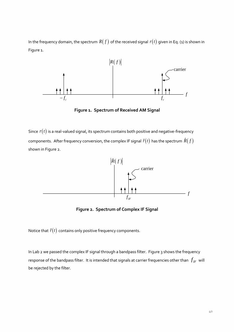
In the frequency domain, the spectrum R f of the received signal r t given in Eq. (1) is shown in
Figure 1.
cfcff
R f
carrier
Figure 1. Spectrum of Received AM Signal
Since r t is a real-valued signal, its spectrum contains both positive and negative-frequency
components. After frequency conversion, the complex IF signal r t has the spectrum R f
shown in Figure 2.
IFff
R f
carrier
Figure 2. Spectrum of Complex IF Signal
Notice that r t contains only positive frequency components.
In Lab 2 we passed the complex IF signal through a bandpass filter. Figure 3 shows the frequency
response of the bandpass filter. It is intended that signals at carrier frequencies other than IFf will
be rejected by the filter.

41
IFff
H f
IFf
Figure 3. Frequency Response of Intermediate-Frequency Filter
Image Signal
Suppose that there is a second signal received along with the signal of Eq. (1), and that this signal is
given by
2
2 2 2 2
2
1 cos 2 ,r IM
p
m tr t A f t
m
(7)
where the carrier frequency IMf happens to be given by
.IM LO IFf f f (8)
If we carry out the analysis of Eqs. (7) and (8), we find that this second signal produces the complex
IF signal 2r t given by
222
2 2
2
1 .IFj f t
r
p
m tr t A e
m
(9)
The spectrum 2R f of this signal is shown in Figure 4.
IFff
2R f
carrier
Figure 4. Spectrum of the Image Signal
42
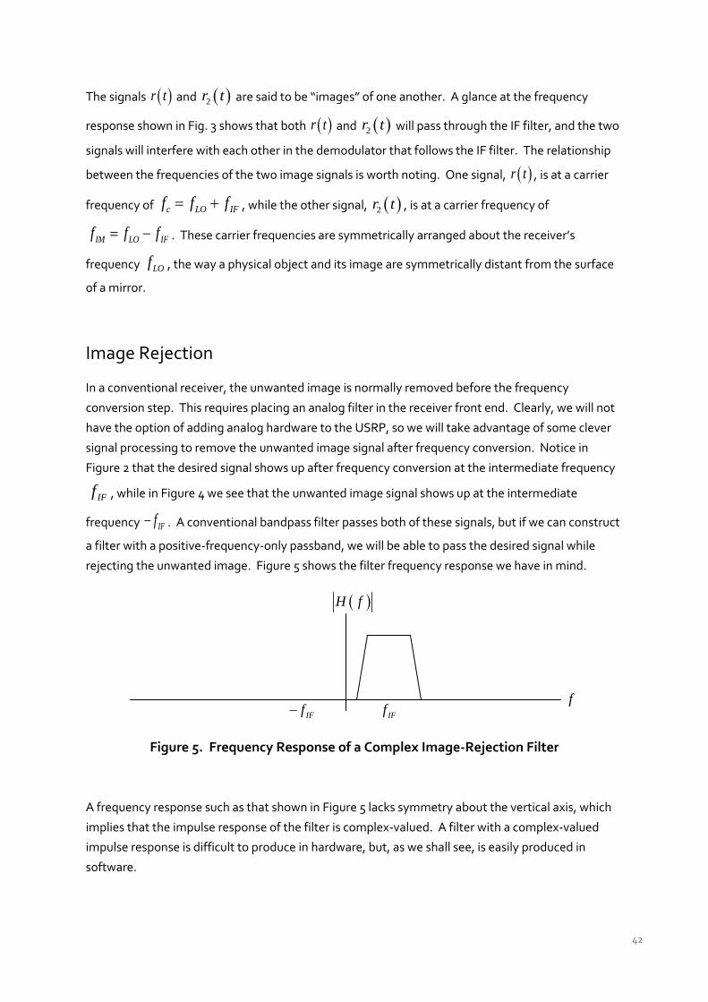
The signals r t and 2r t are said to be “images” of one another. A glance at the frequency
response shown in Fig. 3 shows that both r t and 2r t will pass through the IF filter, and the two
signals will interfere with each other in the demodulator that follows the IF filter. The relationship
between the frequencies of the two image signals is worth noting. One signal, r t , is at a carrier
frequency of c LO IFf f f , while the other signal, 2r t , is at a carrier frequency of
IM LO IFf f f . These carrier frequencies are symmetrically arranged about the receiver’s
frequency LOf , the way a physical object and its image are symmetrically distant from the surface
of a mirror.
Image Rejection
In a conventional receiver, the unwanted image is normally removed before the frequency
conversion step. This requires placing an analog filter in the receiver front end. Clearly, we will not
have the option of adding analog hardware to the USRP, so we will take advantage of some clever
signal processing to remove the unwanted image signal after frequency conversion. Notice in
Figure 2 that the desired signal shows up after frequency conversion at the intermediate frequency
IFf , while in Figure 4 we see that the unwanted image signal shows up at the intermediate
frequency IFf . A conventional bandpass filter passes both of these signals, but if we can construct
a filter with a positive-frequency-only passband, we will be able to pass the desired signal while
rejecting the unwanted image. Figure 5 shows the filter frequency response we have in mind.
IFff
H f
IFf
Figure 5. Frequency Response of a Complex Image-Rejection Filter
A frequency response such as that shown in Figure 5 lacks symmetry about the vertical axis, which
implies that the impulse response of the filter is complex-valued. A filter with a complex-valued
impulse response is difficult to produce in hardware, but, as we shall see, is easily produced in
software.
43
On a practical note, an analog image rejection filter must be tunable if the receiver is to be capable
of receiving signals at a range of carrier frequencies cf . To make the filter tunable, it usually must
be kept simple, which constrains the order of the filter to be low. Second-order filters are common
in this application. A low-order filter cannot do a very thorough job of rejecting signals at the
unwanted image frequency. In contrast, the complex image rejection filter of Figure 5 is centered at
a fixed intermediate frequency, and does not have to be tunable. The quality of image rejection is
limited only by the ability of the filter to reject signals at negative frequencies.
4.3 Pre-Lab A complex filter has been provided in ChebyshevHilbert.gvi. Your task is to create a program to find
the frequency response of this filter. There are several ways in which this can be done, and the
method is left up to you.
1. Set the filter up with
a sampling frequency of 1MS/s
a high cutoff frequency of 105 kHz
a low cutoff frequency of 95 kHz
order 5
you can accept the default ripple value of 0.1 dB.
2. Plot the magnitude of the frequency response in decibels over the frequency range
200 kHz to 200 kHz . (The frequency axis must be a linear scale; this is not a Bode plot.)
Note:
The input to the filter is an array of complex numbers, as is the output. If you choose to
measure the frequency response by inputting sinusoidal signals at a range of frequencies, you
must use complex sinusoids 2j fte rather than conventional sinusoids cos 2 ft so that
negative frequencies can be distinguished from positive frequencies.
4.4 Lab Procedure 1. Connect a loopback cable and attenuator between the TX 1 and RX 2 connectors. Connect the
USRP to your computer and plug in the power to the USRP. .
44
2. Open the AM transmitter and receiver functions that you created for Lab 2.
Ensure that the transmitter is set up to use
Carrier Frequency: 915.1 MHz
IQ Rate: Not critical. 200 kHz
Gain: Not critical. 0 dB
Active Antenna: TX1
Message Length: 200,000 samples gives a good block of data to work with.
Modulation Index: Start with 1.0.
Start Frequency, Delta Frequency, Number of Tones: Not critical, but keep the highest
frequency below 5 kHz. Three tones seems to work well.
Ensure that the receiver is set up to use
Carrier Frequency: 915 MHz
IQ Rate: 1 MHz
Gain: Not critical. 0 dB
Active Antenna: RX2
Number of Samples: Same value as the transmitted message length.
Run the transmitter and receiver and verify that the demodulated message appears at the
receiver output.
3. Modify the receiver functions by adding components to indicate the strength of the received
carrier. To do this, recall that the output of an AM demodulator is
1 .o
p
m tr t D
m
(10)
Since the message m t has an average value of zero, the average of or t will be the
received carrier D . You can average or t by using a lowpass filter whose cutoff frequency is

45
below the lowest frequency component of m t , or by finding a suitable signal-averaging
function.
Run the transmitter and receiver and record the value of the received carrier D .
4. Power Spectrum
Add the FFT Power Spectrum for 1 Chan (CDB) from the ExternalFiles folder to your receiver.
Obtain the “time signal” input from the waveform produced by Fetch Rx Data. Attach a
Boolean constant set to True to the “dB On” input. Attach a waveform graph to the “Power
Spectrum/PSD” output. Change the label on the horizontal axis of the waveform graph to
“Frequency.”
Run the transmitter and the receiver. Take a screenshot of the spectrum of the received signal.
The spectrum should correspond to the one shown in Figure 2.
5. Use Eq. (8) to determine the image frequency IMf . Set the frequency of the transmitter to
IMf . Run the transmitter and receiver and record the value of the received carrier 2D .
Compute the image rejection ratio (IRR) given by
10
2
IRR 20log .D
D (11)
(You should get a result near zero dB.)
Take another screenshot of the spectrum of the received image signal. This time, the
spectrum should correspond to the one shown in Figure 4.
6. Replace the bandpass filter in your receiver with ChebyshevHilbert.gvi. Set the transmitter’s
carrier frequency to 915.1 MHzcf , run the transmitter and receiver, and measure D . Now
set the transmitter’s carrier frequency to IMf , run the transmitter and receiver, and measure
2D . Calculate the IRR and compare with the result you obtained in Step 5.
46
7. Save your modified receiver in a file whose name includes the letters “AMImageRx” and your
initials (e.g. AMImageRx_BAB.gvi).
8. Challenge Question (Familiarity with the Hilbert transform is assumed.)
Suppose in Step 6 you want to receive the signal at carrier frequency IMf rather than the one at
carrier frequency cf . Modify ChebyshevHilbert.gvi to make this happen. (Hint: A single sign
change in an appropriate place in the MathScript block is all that is required.)
4.5 Report
Prelab
Hand in documentation for the program you created to measure the frequency response of
ChebyshevHilbert.gvi. Hand in documentation for the modified receiver. Also include
documentation for any additional sub-functions you may have created. To obtain documentation,
print out legible screenshots of the front panel and block diagram.
Submit the frequency response plot from Step 2 of the Prelab.
Lab
Submit the functions you created to measure the frequency response of ChebyshevHilbert.gvi.
Submit the functions for the modified receiver. Also submit any additional sub-functions you may
have created. Be sure your files adhere to the naming convention described in the instructions
above.
Resubmit documentation for any functions you modified during the lab.
Submit the spectrum graphs required in Steps 4 and 5.
Submit your image rejection ratio computations and results from Steps 5 and 6.

47
If you completed the challenge question (Step 8), show how you modified ChebyshevHilbert.gvi and
describe how you verified the result.

48

49
L A B 5
Double-Sideband Suppressed-Carrier

50
Prerequisite: Lab 2 – Amplitude Modulation
5.1 Objective This laboratory exercise introduces suppressed-carrier modulation. A simple scheme for phase and
frequency synchronization is introduced in implementing the demodulator.
5.2 Background
Double-Sideband Suppressed-Carrier
Amplitude modulation is inherently inefficient because the largest part of the transmitted power is
contained in the carrier. In suppressed-carrier schemes the carrier is simply not transmitted. There
are two common suppressed-carrier techniques in use, double-sideband suppressed-carrier (DSB-
SC) and single-sideband (SSB). Double-sideband suppressed-carrier modulation is identical to AM,
except that the carrier is omitted.
If m t is a baseband “message” signal and cos 2 cf t is a “carrier” signal at carrier frequency
cf , then we can write the DSB-SC signal g t as
cos 2 .cg t Am t f t (1)
For the special case in which cos 2p mm t m f t , we can write
cos 2 cos 2
cos 2 cos 2 .2 2
p m c
p p
c m c m
g t Am f t f t
Am Amf f t f f t
(2)
The two terms in Eq. (2) represent the lower and upper sidebands, respectively. There is no carrier
term at frequency cf . Figure 1 is a plot of a 20 kHz carrier modulated by a 1 kHz sinusoid using
DSB-SC modulation.

51
Figure 1. Double-Sideband Suppressed-Carrier Modulation
When the DSB-SC signal arrives at the receiver, it has the form
cos 2 ,cr t Dm t f t (3)
where D is a constant, usually much smaller than A , and the angle represents the difference in
phase between the transmitter and receiver carrier oscillators. If the receiver’s carrier oscillator (the
“local” oscillator) is set to the same frequency as the transmitter’s carrier oscillator, the USRP will
generate the two demodulated signals
cos , and2
sin .2
I
Q
Dr t m t
Dr t m t
(4)
The Fetch Rx Data provides these demodulated signals as a single complex-valued signal r t given
by
cos sin2 2
.2
j
D Dr t m t j m t
Dm t e
(5)
It is tempting to suppose that the message m t can be extracted from r t by taking the
magnitude of the complex signal. Unfortunately, the magnitude of r t is
,2
rDr t m t (6)
where the absolute value represents unwanted distortion of the message signal. It is more
productive to use the in-phase (real part) signal Ir t given in Eq. (4). The cos factor of Ir t
52
represents a gain constant. Unfortunately, the value of this gain constant is not under user control,
and might be small if turns out to have a value near 2 . Moreover, if the receiver’s oscillator
and transmitter’s oscillator differ slightly in frequency, then the phase error will change with
time, causing Ir t to fade in and out. The next section discusses how we can compensate for the
cos term.
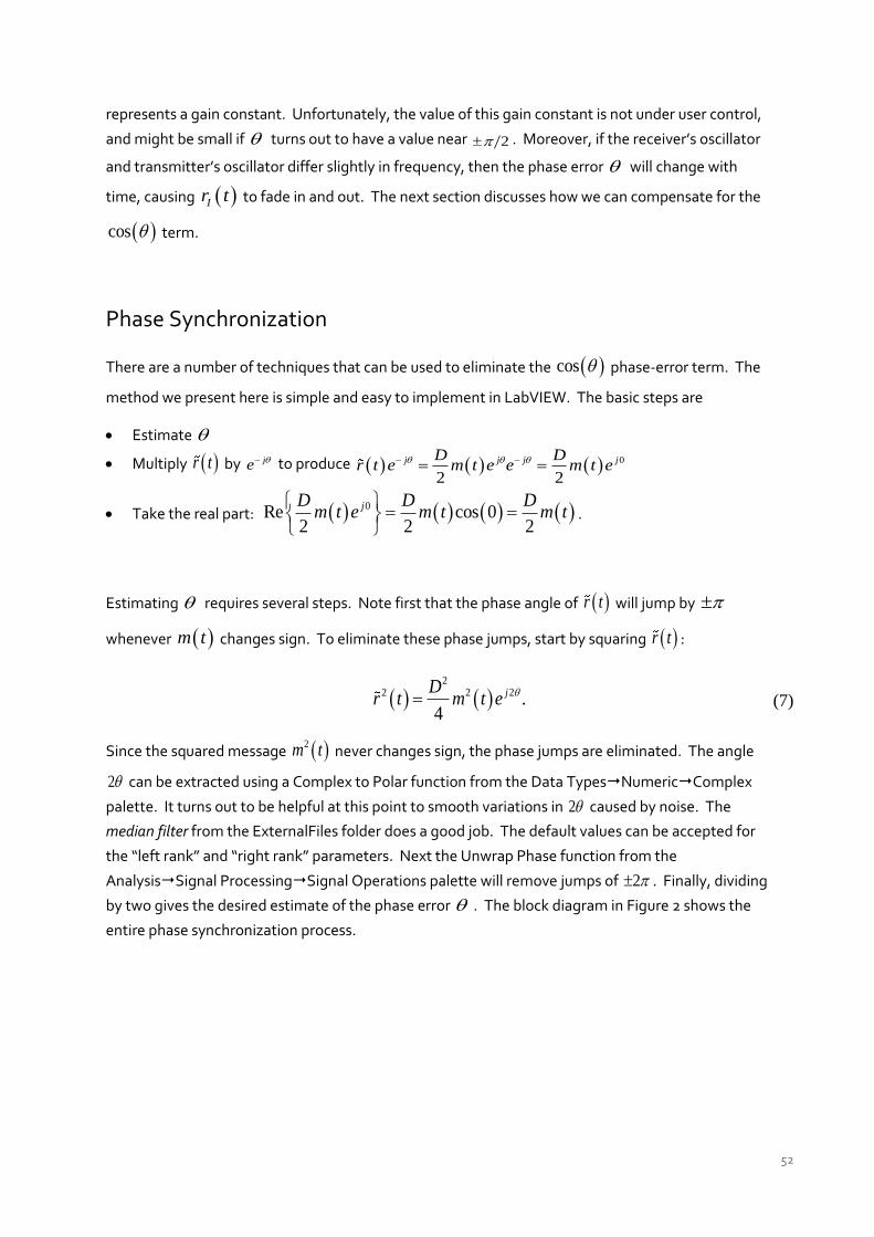
Phase Synchronization
There are a number of techniques that can be used to eliminate the cos phase-error term. The
method we present here is simple and easy to implement in LabVIEW. The basic steps are
Estimate
Multiply r t by je to produce 0
2 2
j j j jD Dr t e m t e e m t e
Take the real part: 0Re cos 02 2 2
jD D Dm t e m t m t
.
Estimating requires several steps. Note first that the phase angle of r t will jump by
whenever m t changes sign. To eliminate these phase jumps, start by squaring r t :
2
2 2 2 .4
jDr t m t e (7)
Since the squared message 2m t never changes sign, the phase jumps are eliminated. The angle
2 can be extracted using a Complex to Polar function from the Data TypesNumericComplex
palette. It turns out to be helpful at this point to smooth variations in 2 caused by noise. The
median filter from the ExternalFiles folder does a good job. The default values can be accepted for
the “left rank” and “right rank” parameters. Next the Unwrap Phase function from the
AnalysisSignal ProcessingSignal Operations palette will remove jumps of 2 . Finally, dividing
by two gives the desired estimate of the phase error . The block diagram in Figure 2 shows the
entire phase synchronization process.
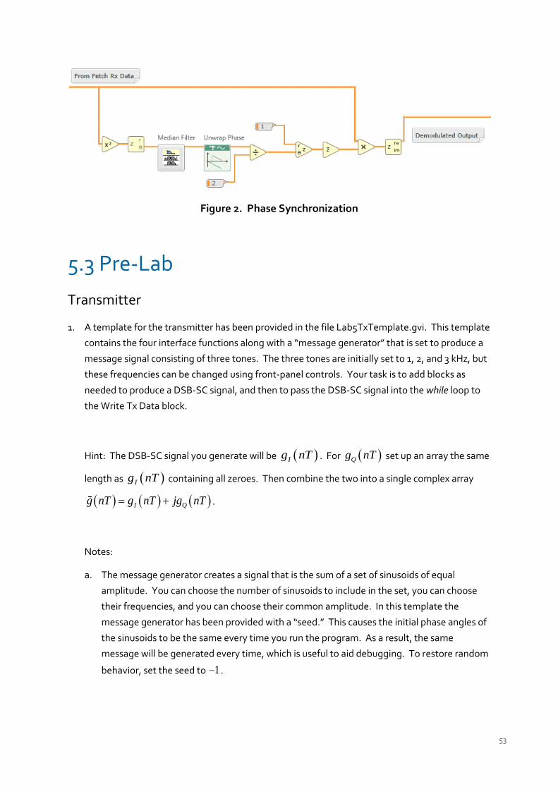
53
Figure 2. Phase Synchronization
5.3 Pre-Lab
Transmitter
1. A template for the transmitter has been provided in the file Lab5TxTemplate.gvi. This template
contains the four interface functions along with a “message generator” that is set to produce a
message signal consisting of three tones. The three tones are initially set to 1, 2, and 3 kHz, but
these frequencies can be changed using front-panel controls. Your task is to add blocks as
needed to produce a DSB-SC signal, and then to pass the DSB-SC signal into the while loop to
the Write Tx Data block.
Hint: The DSB-SC signal you generate will be Ig nT . For Qg nT set up an array the same
length as Ig nT containing all zeroes. Then combine the two into a single complex array
I Qg nT g nT jg nT .
Notes:
a. The message generator creates a signal that is the sum of a set of sinusoids of equal
amplitude. You can choose the number of sinusoids to include in the set, you can choose
their frequencies, and you can choose their common amplitude. In this template the
message generator has been provided with a “seed.” This causes the initial phase angles of
the sinusoids to be the same every time you run the program. As a result, the same
message will be generated every time, which is useful to aid debugging. To restore random
behavior, set the seed to 1 .
54
b. There is a practical constraint imposed by the D/A converters in the USRP: Scale the signals
you generate so that the peak value of g nT does not exceed +/- 1. (Check out the Quick
Scale 1Dfunction in the ExternalFiles folder.)
c. Save your transmitter in a file whose name includes the letters “DSBSCTx” and your initials
(e.g., DSBSCTx_BAB.gvi).
Receiver
2. A template for the receiver has been provided in the file Lab5RxTemplate.gvi. This template
contains the six interface functions along with a waveform graph on which to display your
demodulated output signal.
Complete the program to demodulate the complex array returned by the Fetch Rx Data
function and display the result. Include the phase synchronization of Figure 2. Also, to help in
debugging, include a graph to display the phase error vs. time.
Save your receiver in a file whose name includes the letters “DSBSCRx” and your initials.
Questions
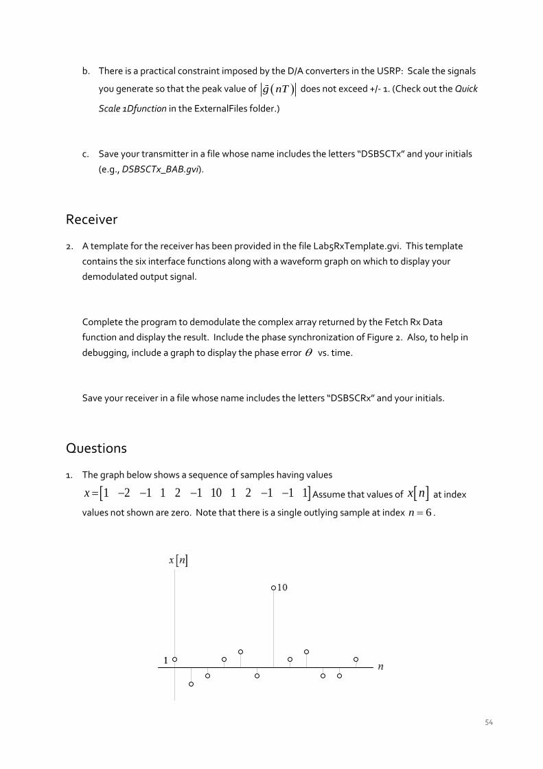
1. The graph below shows a sequence of samples having values
1 2 1 1 2 1 10 1 2 1 1 1x Assume that values of x n at index
values not shown are zero. Note that there is a single outlying sample at index 6n .

55
Suppose we have a simple median filter than produces an output y n given by
median 2 , , 2 , n 0, ,11.y n x n x n
Find y n for the sample sequence x n shown.
2. Suppose the receiver’s carrier oscillator differs in frequency from the transmitter’s oscillator by
a small offset f . Modify Eqs. (4) and (5) to include the frequency offset.
5.4 Lab Procedure 1. Connect a loopback cable and attenuator between the TX 1 and RX 2 connectors. Connect the
USRP to your computer and plug in the power to the USRP. Run LabVIEW and open the
transmitter and receiver that you created in the prelab.
2. Ensure that the transmitter is set up to use
Carrier Frequency: 915 MHz
IQ Rate: Not critical. 200 kHz
Gain: Not critical. 0 dB
Active Antenna: TX1
Message Length: 200,000 samples gives a good block of data to work with.
Start Frequency, Delta Frequency, Number of Tones: Not critical, but keep the highest
frequency below 5 kHz. Three tones seems to work well.
3. Ensure that the receiver is set up to use
Carrier Frequency: 915 MHz
IQ Rate: 200 kHz
Gain: Not critical. 0 dB
Active Antenna: RX2
Number of Samples: Same value as the transmitted message length.
56
Run the transmitter, then run the receiver. After a few seconds, stop the receiver using the
STOP button, then stop the transmitter (using the STOP button). Use the horizontal zoom
feature on the graph palette to expand the “message” waveform in the transmitter and the
“demodulated output” waveform in the receiver. Both waveforms should be identical, except
for scaling.7
4. Modify your receiver to compute Ir t without phase synchronization and Ir t with phase
synchronization. Plot both outputs on the same graph. Run the receiver several times and
observe the outputs. Can you see the effect of the cos term on the unsynchronized output?
5. Try using your AM receiver from Lab 2 to demodulate the DSB-SC signal. Note that you will
need to offset the transmitter frequency to 915.1 MHz. Run the transmitter and receiver. Take
a screenshot of both the transmitted message and the demodulated output. Be sure to expand
the time base so that the waveforms can be clearly seen. Was the envelope detector in the AM
receiver able to correctly demodulate the DSB-SC signal?
6. The phase synchronizer can also correct for modest frequency offsets. Use the DSB-SC
transmitter and receiver, and offset the frequency of the transmitter by 10 Hz. Run the
transmitter and receiver. Take a screenshot of the transmitted message, the unsynchronized
demodulated output, and the synchronized demodulated output. Be sure to expand the time
base so that the waveforms can be clearly seen. Verify that the synchronized demodulated
output is correct, except possibly for being inverted.
Repeat for frequency offsets of 100 Hz and 1 kHz. Can your phase synchronizer handle the 1
kHz case?
7 The demodulated output may be inverted. This is a consequence of squaring the signal in the phase
synchronization process. An error of 2 in the angle 2 is no error at all, but when the angle is divided by
two, the error becomes .

57
5.5 Report
Prelab
Hand in documentation for your transmitter and receiver. Also include documentation for any
additional functions you may have created. To obtain documentation, print out legible screenshots
of the front panel and block diagram.
Submit your answers to the Questions at the end of the Prelab section.
Lab
Submit the program you created to implement the DSB-SC transmitter and receiver. Also submit
any additional functions you may have created. Be sure your files adhere to the naming convention
described in the instructions above. Resubmit documentation for any functions you modified
during the lab.
Describe the effect on the demodulated signal of the cos term, as described in Step 4.
Submit the graphs required in Step 5. Discuss whether DSB-SC can be properly demodulated using
an envelope detector.
Submit the graphs required in Step 6. Comment on whether your phase synchronizer was able to
compensate for frequency offsets of 100 Hz and 1 kHz.

58

59
L A B 6
Frequency Modulation

60
6.1 Objective This laboratory exercise introduces frequency modulation. This lab exercise is a nice illustration of
the utility of the software defined radio approach, since the algorithms for creating and
demodulating FM in software are much simpler than those used in the traditional hardware
approach.
6.2 Background
Frequency Modulation
Frequency modulation (FM) was introduced by E.A. Armstrong in the 1930’s as an alternative to the
AM commonly in use at the time for broadcasting. The advantage to frequency modulation is that,
for a given transmitted power, the signal-to-noise ratio is much higher at the receiver output than it
is for AM. The digital version of FM, frequency-shift keying, has been in use since an even earlier
date.
In FM, the frequency of the carrier is modulated to follow the amplitude of the message signal. To
be more specific, if m t is a message signal with peak value pm , then the instantaneous frequency
f t of the carrier is given by
,c ff t f k m t (1)
where cf is the carrier frequency and fk is a proportionality constant called the “frequency
sensitivity.” The term fk m t is called the “frequency deviation” of the instantaneous frequency
from the carrier frequency, and the peak frequency deviation f pf k m is an important FM
system parameter. Given the instantaneous frequency, we can find the total instantaneous angle
t of the carrier by integrating the instantaneous frequency. That is,
0
0
2
2 2 0 .
t
t
c f
t f d
f t k m d
(2)

61
Since the initial angle 0 is of no consequence, we can simplify the equations by taking
0 0 . The transmitted FM signal is then given by
0
0
cos
cos 2 2
cos 2 2 .
c
t
c c f
t
c c p
g t A t
A f t k m d
A f t f m m d
(3)
Figure 1 shows a 2 kHz carrier frequency modulated by a 200 Hz sinusoidal message.
To create an FM signal using the USRP, the message signal is normalized to a peak value of one,
multiplied by 2 f and integrated to give 0
2t
pf m m d . Next, the complex-valued
signal g t is formed, where
02
.
t
pj f m m d
cg t A e
(4)
The complex-valued signal g t is sent to the Write Tx Data function, and the USRP produces the
FM signal.
The only tricky step in generating an FM signal is integrating the message. In discrete time we have
Figure 1. Frequency Modulated Signal
62
0
0
,nt
k
x d x nT T
(5)
where T is the reciprocal of the IQ sample rate. If we write
0
,n
k
y n x nT T
(6)
then
1
0 0
1
.
n n
k k
y n y n x nT T x nT T
x nT T
(7)
Equation (7) is the difference equation of an IIR filter. This filter can be implemented using the IIR
Filter function found in the AnalysisSignal ProcessingFiltersIIR Filtering palette. Use a
“forward coefficients” array of T and a “reverse coefficients” array of 1 1 .
Demodulation
FM demodulation is much easier to carry out using the USRP than it is using conventional
hardware. The signal provided by the Fetch Rx Data function is r t given by
02
.
t
pj f m m d
rr t A e
(8)
This is identical to the expression given by Eq. (4), except for the magnitude rA and the presence of
noise (not shown in the expression). The angle of r t is easily extracted using a Complex to Polar
function.8 Unwrap the angle before proceeding to the next step. Next, the unwrapped angle is
differentiated, giving 2 2p ff m t m k m t . This result should be passed through a
lowpass filter, since the differentiation step tends to enhance high-frequency noise.
To implement the differentiator, we recognize that in discrete time,
8 For those familiar with conventional FM demodulation, this step implements the limiter.

63
1
.1
dx t x n x n
dt
(9)
The differentiator can be implemented using an FIR Filter function from the AnalysisSignal
ProcessingFilters FIR Filtering palette. For the “FIR coefficients” array use 1 1 .
6.3 Pre-Lab
Transmitter
1. A template for the transmitter has been provided in the file Lab6TxTemplate.gvi. This template
contains the four interface functions along with a “message generator” that is set to produce a
message signal consisting of three tones. The three tones are initially set to 1, 2, and 3 kHz, but
these frequencies can be changed using front-panel controls. Your task is to add blocks as
needed to produce the signal g t of Eq.(4), and then to pass this signal to the Write Tx Data
block. Set the carrier level cA to a constant value of 0.9. Figure 2 shows how to implement the
FM modulator described by Eq. (4).
Figure 2. FM Modulator
Save your transmitter in a file whose name includes the letters “FMTx” and your initials (e.g.,
FMTx_BAB.gvi).
Receiver
2. A template for the receiver has been provided in the file Lab6RxTemplate.gvi. This template
contains the six interface functions along with a waveform graph on which to display your
demodulated output signal.

64
Complete the program to demodulate the complex array returned by Fetch Rx Data and display
the result. Figure 3 shows an implementation of the FM demodulator, including extracting the
angle, unwrapping, differentiation, and lowpass filtering.
Figure 3. FM Demodulator
Save your receiver in a file whose name includes the letters “FMRx” and your initials (e.g.,
FMRx_BAB.gvi).
Questions
1. Find the frequency response of the integrator given by Eq. (7). Compare with the frequency
response of an ideal integrator. Is the discrete-time integrator more like an ideal integrator
when the frequency of the input is low or when it is high?
2. Find the frequency response of the differentiator given by Eq. (9). Compare with the frequency
response of an ideal differentiator. Is the discrete-time differentiator more like an ideal
differentiator when the frequency of the input is low or when it is high?
6.4 Lab Procedure 1. Connect a loopback cable and attenuator between the TX 1 and RX 2 connectors. Connect the
USRP to your computer and plug in the power to the USRP. Run LabVIEW and open the
transmitter and receiver that you created in the prelab.
Note that all graphs in this lab are taken on a linear scale (dB on = False).

65
2. Ensure that the transmitter is set up to use
Carrier Frequency: 915 MHz
IQ Rate: Not critical; 1 MHz
Gain: Not critical. 0 dB
Active Antenna: TX1
Message Length: 200,000 samples gives a good block of data to work with.
Peak Frequency Deviation: 30 kHz seems a good value to start with.
Start Frequency, Delta Frequency, Number of Tones: Not critical, but keep the highest
frequency below 5 kHz. Three tones seems to work well, but you may wish to start with a single
tone to verify operation.
3. Ensure that the receiver is set up to use
Carrier Frequency: 915 MHz
IQ Rate: 1 MHz
Gain: Not critical. 0 dB
Active Antenna: RX2
Number of Samples: Same value as the transmitted message length.
Run the transmitter, then run the receiver. After a few seconds, stop the receiver using the
STOP button, then stop the transmitter (using the STOP button). Use the horizontal zoom
feature on the graph palette to expand the “message” waveform in the transmitter and the
“demodulated output” waveform in the receiver. Both waveforms should be identical, except
for scaling.
4. The bandwidth of an FM signal is notoriously difficult to calculate analytically. J.R. Carson,
writing in the 1920’s, provided a rule of thumb for approximating the bandwidth:
2 ,FMB f B (10)

66
where FMB is the bandwidth of the FM signal, f is the peak frequency deviation of the signal,
and B is the message bandwidth.
Add an FFT Power Spectrum and PSD (ExternalFiles folder) to your transmitter. Obtain the
“time signal” input from the complex baseband waveform that is being sent to the USRP Write
Tx Data. Connect the “Power Spectrum/PSD” output to a waveform graph. Change the label
on the horizontal axis of the graph to “Frequency.” The spectrum you obtain will be identical to
the power spectrum of the actual transmitted FM signal, except that the carrier will appear at
zero hertz, with the lower sideband on the negative-frequency side and the upper sideband on
the positive-frequency side.
To obtain the classic textbook FM spectrum, set the message for a single tone at 1 kHz. Run the
transmitter and obtain power spectra of the transmitted signal for peak frequency deviations of
1 kHz, 5 kHz, and 30 kHz. Take a screenshot of the power spectrum for each case. Be sure to
scale the horizontal axis so that each spectrum is visible. Annotate your spectra to show the
Carson’s rule bandwidth, Eq. (10), for each case.
For a more realistic set of FM spectra, set the message for three tones at 1 kHz, 2 kHz, and 3
kHz. Run the transmitter and obtain power spectra of the transmitted signal for peak
frequency deviations of 1 kHz, 5 kHz, and 30 kHz. Take another set of screenshots of the power
spectrum for each case. Be sure to scale the horizontal axis so that each spectrum is visible.
Annotate your spectra to show the Carson’s rule bandwidth for each case.
5. One of the more curious, but also very useful, phenomena associated with FM is the so-called
“capture effect.” To observe this effect you will need to modify your transmitter to
simultaneously generate two FM baseband signals at different carrier levels.
In your transmitter, duplicate the Basic Multitone to generate a second message signal. Your
two Basic Multitone functions can share “sampling info,” but each should have its own set of
start frequency, stop frequency, and #tones. The constants “T” and “1” can be shared as well.

67
Inside the transmitter’s while loop, create a second modulator, including a second integrator.
Create two front panel controls, “Carrier 1” and “Carrier 2” to set the carrier levels cA for each
modulator. For simplicity, the two modulators can share a common peak frequency deviation.
Add the two FM baseband signals produced by your modulators together and send the sum to
the Build Waveform function that feeds the USRP Write Tx Data.
Set up your first message generator for three tones at 1 kHz, 2 kHz and 3 kHz. Set up the
second message generator for three tones at 100 Hz, 200 Hz, and 300 Hz. These two message
signals should be easy to distinguish at the receiver. Set the peak frequency deviation to 30,000
Hz.
At this point test your system by setting carrier 1 to 0.9 and carrier 2 to zero. Run the
transmitter and receiver and make sure that the receiver output matches message 1. Next, set
carrier 1 to zero and carrier 2 to 0.9 and make sure that the receiver output matches message 2.
At the receiver, add an FFT Power Spectrum and PSD to view the spectrum of the baseband
output. Label the horizontal axis “Frequency” and set the range to show 0 to 5000 Hz. It will be
easier to distinguish message 1 from message 2 in the frequency domain than in the time
domain.
Now you are ready to observe the capture effect! Start by setting carrier 1 to 0.4 and carrier 2
to 0.6. Run the transmitter and receiver. Take a screenshot of the receiver’s baseband output
spectrum. Repeat with carrier 1 set to 0.5 and carrier 2 set to 0.5. Repeat a third time with
carrier 1 set to 0.6 and carrier 2 set to 0.4. You should find that in the first and third cases, the
receiver demodulates (captures) only the stronger signal. This is the capture effect: If two FM
signals are received at the same carrier frequency, the receiver will demodulate the stronger
signal, even if the stronger carrier is only slightly stronger than the weaker one.
68
6.5 Report
Prelab
Hand in documentation for your transmitter and receiver programs. Also include documentation
for any additional functions you may have created. To obtain documentation, print out legible
screenshots of the front panel and block diagram.
Submit your answers to the Questions at the end of the Prelab section.
Lab
Submit the functions you created to implement the FM transmitter and receiver. Also submit any
additional functions you may have created. Be sure your files adhere to the naming convention
described in the instructions above. Resubmit documentation for any functions you modified
during the lab.
Submit the graphs required in Step 4. Be sure to indicate on each graph the bandwidth estimated
by Carson’s rule. With reference particularly to the spectra for the three-tone message, does an FM
signal always have sidebands that are symmetrical with respect to the carrier?
Submit the graphs required in Step 5. Explain briefly how this sequence of graphs demonstrates
the capture effect.
69
L A B 7
Amplitude-Shift Keying

70
Prerequisite: Lab 2 – Amplitude Modulation
7.1 Objective Amplitude-shift keying (ASK) is the simplest form of digital modulation. We will use it to provide an
introduction to digital communications, and as a vehicle to introduce some of the features that are
common to digital communication systems, such as symbol mapping, pulse shaping, matched
filtering, threshold detection, and pulse synchronization.
In this lab project, design of the transmitter and design of the receiver each present challenges and
opportunities for investigation. The lab project is consequently divided into several parts. The
transmitter part investigates creation of the ASK signal and the effect of transmitted pulse shape
on the bandwidth of the transmitted signal. The receiver part investigates demodulation, matched
filtering, and signal detection. There is a third part investigating alignment of the receiver and
transmitter bit streams.
7.2 Part 1: Transmitter
Background
ASK is simply AM with a binary message waveform. To illustrate, suppose m t is a binary
message represented in a polar, non-return-to-zero (NRZ) format, as shown in Figure 1.
Figure 1. Binary Message Waveform
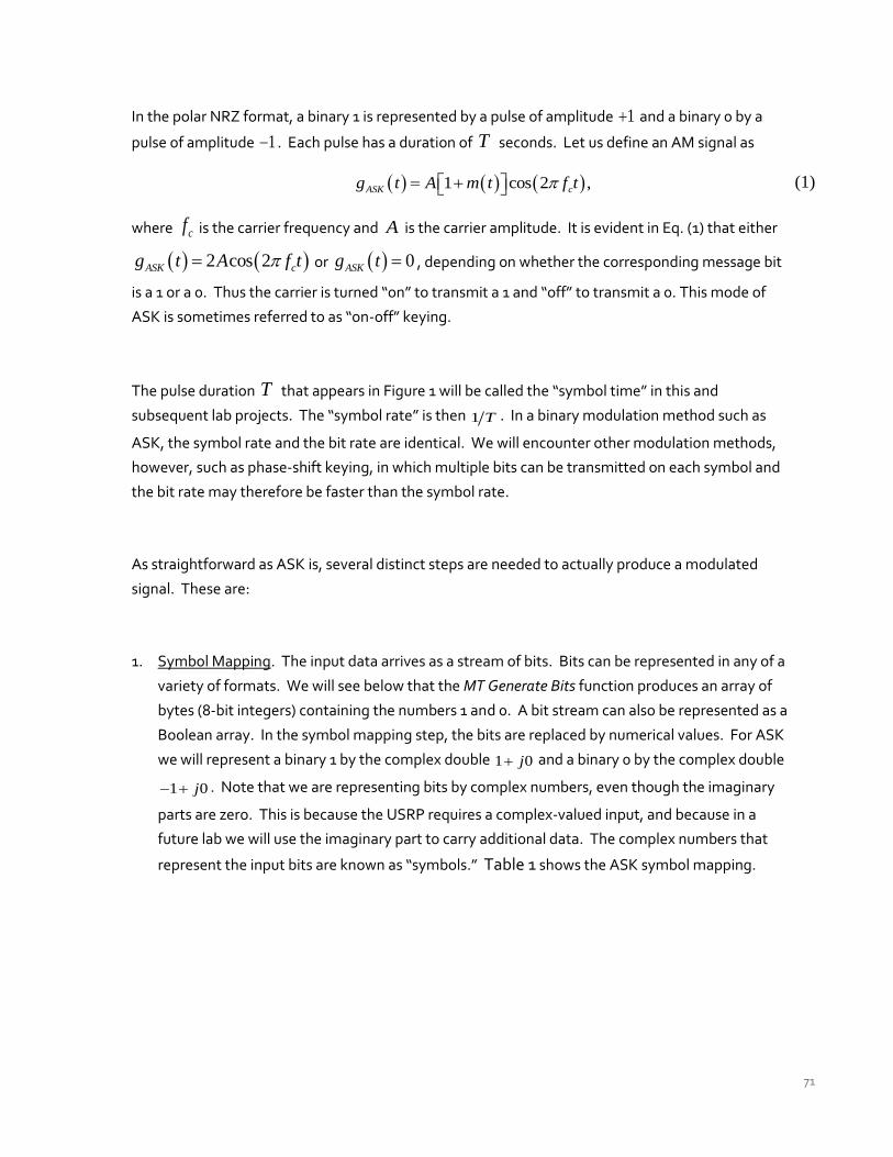
71
In the polar NRZ format, a binary 1 is represented by a pulse of amplitude 1 and a binary 0 by a
pulse of amplitude 1 . Each pulse has a duration of T seconds. Let us define an AM signal as
1 cos 2 ,ASK cg t A m t f t (1)
where cf is the carrier frequency and A is the carrier amplitude. It is evident in Eq. (1) that either
2 cos 2ASK cg t A f t or 0ASKg t , depending on whether the corresponding message bit
is a 1 or a 0. Thus the carrier is turned “on” to transmit a 1 and “off” to transmit a 0. This mode of
ASK is sometimes referred to as “on-off” keying.
The pulse duration T that appears in Figure 1 will be called the “symbol time” in this and
subsequent lab projects. The “symbol rate” is then 1 T . In a binary modulation method such as
ASK, the symbol rate and the bit rate are identical. We will encounter other modulation methods,
however, such as phase-shift keying, in which multiple bits can be transmitted on each symbol and
the bit rate may therefore be faster than the symbol rate.
As straightforward as ASK is, several distinct steps are needed to actually produce a modulated
signal. These are:
1. Symbol Mapping. The input data arrives as a stream of bits. Bits can be represented in any of a
variety of formats. We will see below that the MT Generate Bits function produces an array of
bytes (8-bit integers) containing the numbers 1 and 0. A bit stream can also be represented as a
Boolean array. In the symbol mapping step, the bits are replaced by numerical values. For ASK
we will represent a binary 1 by the complex double 1 0j and a binary 0 by the complex double
1 0j . Note that we are representing bits by complex numbers, even though the imaginary
parts are zero. This is because the USRP requires a complex-valued input, and because in a
future lab we will use the imaginary part to carry additional data. The complex numbers that
represent the input bits are known as “symbols.” Table 1 shows the ASK symbol mapping.

72
Table 1. ASK Symbol Mapping
Bit Value Symbol
0 1 0j
1 1 0j
2. Upsampling. We will see below that the symbols are carried on pulses whose shape is
important in establishing the bandwidth of the transmitted signal. As a first step toward
replacing symbols by pulses, we will place 1L zeroes after each symbol. This produces a
sample interval of
,x
TT
L (2)
or a sample rate of
1 1
.x
LT T
(3)
A higher upsampling factor L makes the D/A conversion in the transmitter easier, but requires
faster digital processing. We will use 20L in this lab project. The Upsample function is
made to order for implementing this step.
3. Pulse Shaping. If the upsampled signal is applied to a filter whose impulse response TXg n is
a rectangular pulse of unit amplitude and length L samples, then at the filter output, each
symbol will be represented by a rectangular pulse. Figure 2 shows the effect of upsampling and
filtering. Waveform (a) represents the symbol sequence, with symbols occurring every T
seconds. Waveform (b) shows the symbol sequence after upsampling. Waveform (c) shows the
upsampled symbol sequence after filtering by the pulse-shaping filter. Note that waveform (c)
is a discrete-time version of the polar NRZ message waveform shown in Figure 1. An important
advantage to following this particular sequence of steps to generate the message waveform is
that the impulse response TXg n of the pulse-shaping filter does not have to be a rectangular
73
pulse. We will see later in this lab project that there can be advantages to using other pulse
shapes.
(a)
(b)
(c)
Figure 2. (a) Symbol sequence, (b) Upsampled symbol sequence, (c) Filtered
upsampled symbol sequence.
4. Modulation. If m n represents the message waveform at the transmitter filter output, then
the final step is to apply Eq. (4):
1 ,ASKg n A m n (4)
where the constant A is chosen to keep the magnitude of ASKg n less than 1. This signal
can be sent to the USRP transmitter. The USRP transmitter will perform the D/A conversion
and multiplication by the carrier cos 2 cf t .
74
Prelab
1. Create a program to generate an ASK signal using the USRP. A template for the
transmitter has been provided in the file ASKTxTemplate.gvi. This template contains the
four functions for interfacing with the USRP along with MT Generate Bits from the
Modulation Toolkit. MT Generate Bits will create a pseudorandom sequence of bits that can
serve as a data sequence for testing your ASK system. Note that by default, MT Generate
Bits will produce the same sequence of bits every time you run the program. This is useful
for debugging, but if you would like to generate a different sequence of bits every time,
wire a random number to the “seed in” input. The steps below contain details about how to
create the required transmitter.
2. First do the symbol mapping, as shown in Table 1. This will convert the integers 0,1 from
MT Generate Bits to complex doubles 1 0j . In future lab projects, where the symbol
mapping may be more elaborate, this might be implemented as a sub-vi. In this lab project
the symbol mapping is relatively simple, and a sub-vi implementation is optional.
3. Upsample using Upsample from the AnalysisSignal ProcessingSignal Operation
subpalette. In this lab project you are given control inputs to set the symbol rate 1 T and
the IQ rate 1 xT . Set the symbol rate to 10,000 symbols/s and the IQ rate to
3200 10 Sa/s . Use these two inputs to calculate the upsampling factor L .
3. Use MT Generate Filter Coefficients from the Modulation Toolkit to generate the pulse
shaping filter. (MT Generate Filter Coefficients can be found on the
AnalysisCommunicationsDigitalUtilities subpalette.) Set the modulation type to
ASK, and the pulse-shaping filter “samples per symbol” to your calculated value of L .
Create a front-panel control for “pulse shaping filter” and set this initially to “none.” The
setting of “none” will generate rectangular pulses. (“none” does not mean that there is no
filter!) Wire the “pulse shaping filter coefficients” output to the “Y” input of a Convolution.
The Convolution is available from the AnalysisSignal ProcessingSignal Operation
subpalette. Wire the output from your upsampler to the “X” input of the Convolution.
4. Normalize the amplitude of your filtered message signal to a maximum absolute value of 1.
This will be important later when we investigate alternative pulse shapes. Check out the
75
Quick Scale 1D in the ExternalFiles folder for finding the maximum of the absolute value. To
ensure that your scaled message remains complex-valued, use a separate division function
to do the actual scaling. (That is, do not use the MaxY i X i X output of Quick
Scale 1D.)
5. Implement Eq. (4). Let the constant A be 1 2 , so that ASKg n varies between zero and
one. Combine ASKg n with xT using the Build Waveform function provided in the
template to produce the “Baseband Signal.” Note that 1 xT is available as the “actual IQ
rate.” Also connect ASKg n to the “data” input of the Write Tx Data function.
6. An FFT Power Spectrum for 1 Chan has been provided in the template to allow you to
observe the spectrum of the transmitted signal.
This completes construction of the ASK transmitter. Save your transmitter in a file whose
name includes the letters “ASKTx” and your initials (e.g. ASKTx_BAB.gvi).
Lab Procedure
1. Connect a loopback cable and attenuator between the TX 1 and RX 2 connectors of the
USRP. Connect the USRP to your computer and plug in the power to the USRP. Run
LabVIEW and open the transmitter that you created in the prelab.
2. Ensure that the transmitter is set up to use
Carrier Frequency: 915.1 MHz (Note: The 100 kHz offset from the receiver carrier
frequency is deliberate.)
IQ Rate: 200 kHz. Note: This sets the value of 1 xT .
Gain: 0 dB
Active Antenna: TX1
Symbol rate: 10,000 symbols/s

76
Message Length: 1000 bits
Pulse shaping filter: None
Run the transmitter. Use the large STOP button on the front panel to stop transmission
connectors.
3. After running the transmitter, observe the spectrum of the transmitted signal. You should
be able to clearly see the carrier at frequency “zero.” Two additional features are
significant: the bandwidth and the rate of spectral rolloff. Using the Capture Data feature
or using cursors on the Power Spectrum graph, measure the null-to-null bandwidth of the
transmitted signal. Relate this bandwidth to the symbol rate 1 T . The rate of spectral
rolloff is a measure of the interference that your signal will cause to signals using nearby
carrier frequencies. Print a copy of the spectrum for comparison with the spectrum you will
obtain in Step 4 below.
4. Rectangular pulses are rarely used in practice because of the very gradual spectral rolloff
they produce. Change the pulse-shaping filter to “Root Raised” for a root-raised-cosine
filter. Run the program examine the spectrum again. Measure the null-to-null bandwidth
of the transmitted signal. Print a copy of the spectrum and compare the rolloff rate with
the spectrum you obtained using rectangular pulses.
Questions
1. In step 2 you are given 1 10,000 symbols/sT and 31 200 10 Sa/sxT . Find the
corresponding value for the number of samples per symbol L .
2. Relate the symbol rate to the null-to-null bandwidth of the ASK signal for (a) rectangular
and (b) root-raised-cosine pulses.
3. Compare the rates of spectral rolloff of the transmitted signal for rectangular and root-
raised-cosine pulses.

77
7.3 Part 2: Receiver
Background
An ASK receiver begins as an analog AM receiver. We will offset the transmitter and receiver carrier
frequencies by 100 kHz, so that the signal retrieved from the USRP receiver will be an AM signal
having an “intermediate” carrier frequency of 100 kHz. The retrieved AM signal will be passed
through a bandpass “intermediate frequency” filter and then demodulated using an envelope
detector. The envelope detector is implemented by taking the magnitude of the bandpass filter
output, and then lowpass filtering using a second filter. If you completed Lab 2, Amplitude
Modulation, these steps should be familiar.
For digital communications, the lowpass filter should be designed to minimize the effects of noise
and to also minimize the effects of intersymbol interference that can be caused when the filtered
received pulses overlap. The best filter for eliminating noise is a so-called “matched” filter. A
matched filter has a frequency response whose magnitude matches the magnitude of the
frequency response of the transmitter’s pulse-shaping filter. That is, if RXg n is the impulse
response of the receiver’s filter, then we want j j
RX TXG e G e . By using MT Generate
Filter Coefficients at both the transmitter and receiver, we will ensure that the appropriate receiver
filter is chosen to match the pulse-shaping filter at the transmitter.
To complete the digital receiver, several additional steps follow the AM demodulator.
1. Pulse Synchronization. The AM receiver output is an analog baseband signal that must be
sampled once per symbol time, i.e. once every T seconds. Because of filtering and
propagation delays and distortion caused by the communication channel, it is necessary to
determine the optimum time to take these samples. A function PulseAlign(real) has been
provided in the BasicUSRPLabs folder to align the baseband signal so that the sample at index 0
is the correct first sample.
2. Sampling. The Decimate function will sample the aligned baseband waveform at index 0 and
every T seconds thereafter.

78
3. Detection. Once the baseband waveform has been sampled, each sample must be examined to
determine whether it represents a symbol of value 1 or a symbol of value 0.
4. Symbol Mapping. The detected symbol values must be converted to bits. For ASK, this step is
easily included in the detection step.
Prelab
1. A template for the receiver has been provided in the file ASKRxTemplate.gvi. This template
contains the six interface functions for interfacing with the USRP.
We want the receiver to capture two frames of data each time it is run. Since the receiver’s
starting point is random, this will ensure that there will always be one complete frame in the
captured data. Using the message length and symbol rate available from front panel inputs,
and the “Actual IQ Rate” available from Configure Signal, have the receiver calculate the
number of samples in a frame. Then double this number and provide the result as the “number
of samples” input to the Fetch Rx Data.
Fetch Rx Data returns a complex double cluster which makes the “Y” and “dt” components
available. Pass the “Y” complex array through a bandpass filter. Filters can be found in the
ExternalFiles folder in the Files Pane folder in the Files Pane folder. Use a fifth-order Chebyshev
Filter (CDB) with a high cutoff frequency of 110 kHz and a low cutoff frequency of 90 kHz. The
default passband ripple of 0.1 dB is acceptable. The “sampling frequency” input to the filter can
be obtained as the reciprocal of the “dt” component of the waveform returned by Fetch Rx
Data. Note that dt is the same as the “actual IQ rate” returned by Configure Signal. We also
designate this parameter as 1 zT .
2. Extract the real part of the complex array at the output of the Chebyshev bandpass filter
“Filtered X”. To obtain the envelope, take the absolute value and pass the result through a
matched filter. The absolute value functions as a full-wave rectifier. For the matched filter, use
MT Generate Filter Coefficients just as you did for the transmitter. Set the modulation type to
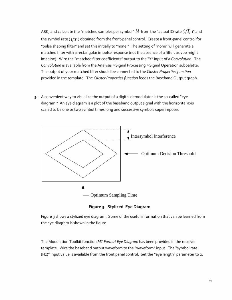
79
ASK, and calculate the “matched samples per symbol” M from the “actual IQ rate (1 zT )” and
the symbol rate (1 T ) obtained from the front-panel control. Create a front-panel control for
“pulse shaping filter” and set this initially to “none.” The setting of “none” will generate a
matched filter with a rectangular impulse response (not the absence of a filter, as you might
imagine). Wire the “matched filter coefficients” output to the “Y” input of a Convolution. The
Convolution is available from the AnalysisSignal ProcessingSignal Operation subpalette.
The output of your matched filter should be connected to the Cluster Properties function
provided in the template. The Cluster Properties function feeds the Baseband Output graph.
3. A convenient way to visualize the output of a digital demodulator is the so-called “eye
diagram.” An eye diagram is a plot of the baseband output signal with the horizontal axis
scaled to be one or two symbol times long and successive symbols superimposed.
Optimum Decision Threshold
Optimum Sampling Time
Intersymbol Interference
Figure 3. Stylized Eye Diagram
Figure 3 shows a stylized eye diagram. Some of the useful information that can be learned from
the eye diagram is shown in the figure.
The Modulation Toolkit function MT Format Eye Diagram has been provided in the receiver
template. Wire the baseband output waveform to the “waveform” input. The “symbol rate
(Hz)” input value is available from the front panel control. Set the “eye length” parameter to 2.

80
4. Place the PulseAlign(real) on your block diagram and wire the baseband output waveform to
the “input waveform” input and wire the calculated M samples/symbol value to the “receiver
sampling factor” input.
Once the baseband waveform is aligned, it can be sampled. Decimate (single shot) can be
obtained from the AnalysisSignal ProcessingSignal Operation subpalette. The “decimating
factor” is M .
5. To determine whether each received sample is more likely to represent a 1 or a 0, the sample
must be compared with a threshold. Use the Mean DBL function from the ExternalFiles folder
to compute the threshold. The result of the comparison is the receiver’s digital output. The
output of the comparison will be a Boolean array. You can convert this array to an integer array
by using a Boolean To Integer function.
This completes construction of the ASK receiver. Save your receiver in a file whose name includes
the letters “ASKRx” and your initials (e.g. ASKRx_BAB.gvi).
Lab Procedure
1. Ensure that the receiver is set up to use
Carrier Frequency: 915.0 MHz
IQ Rate: 1 MHz
Gain: 0 dB
Active Antenna: RX2
Symbol rate: 10,000 symbols/s
Message length: 1000 bits
Pulse shaping filter: none
2. Run the transmitter, then run the receiver. Once the receiver has acquired a block of data, you
may stop the transmitter.

81
3. Use the horizontal zoom feature on the Baseband Output graph palette to expand the
demodulated waveform so that you can see individual pulses. Ideally, rectangular pulses
passed through the receiver’s matched filter should produce triangular output pulses. Note
whether the demodulated pulses have the expected shape.
4. Observe the eye diagram. Make note of the optimum sampling time and the presence of
intersymbol interference.
5. Change the “pulse shaping filter” control at both the transmitter and the receiver to “Root
Raised” for root-raised-cosine filters. Setting both the transmitter and receiver filters will
ensure that the filters remain matched for optimum performance in the presence of noise. The
cascade of two root-raised-cosine filters produces a raised-cosine pulse at the receiver filter
output. The raised-cosine pulse is designed to minimize, or ideally eliminate, intersymbol
interference.
Run the transmitter and then run the receiver. Once the receiver has acquired a block of data,
you may stop the transmitter. Observe the baseband output signal and the eye diagram.
Comment on the changes to the eye diagram. Has intersymbol interference been reduced?
6. To see the effect of pulse synchronization, move the waveform input of MT Format Eye Diagram
to the “aligned waveform” output of PulseAlign(real). Run the transmitter and receiver again.
Observe the eye diagram. What is the optimum sampling time now?
82
Questions
1. Give a formula showing how the IQ Sampling Rate, the symbol rate 1 T , and the number of
samples per symbol M are related. Determine the value of M for an IQ Sampling Rate of 1
MHz and a symbol rate of 10,000 symbols/s.
2. Note that the IQ sampling rate at the receiver is different from the IQ sampling rate at the
transmitter. Using a higher IQ sampling rate requires faster digital processing. What is the
advantage to using a higher IQ sampling rate at the receiver? (Hint: It has something to do
with the action of the PulseAlign(real) and the value of M .)
3. Compare the rectangular and raised-cosine pulse shapes by examining the eye diagrams. What
evidence for intersymbol interference do you see in each case?
4. Using root-raised-cosine pulses and receiver filtering, observe the eye diagram when the input
of MT Format Eye Diagram is set to “baseband output” and when the input of MT Format Eye
Diagram is set to the “aligned waveform” output of PulseAlign(real). What function is
PulseAlign(real) performing?
5. The transmitter is programmed to generate the same “frame” of 1000 symbols over and over.
The receiver grabs a single block of 2000 symbols each time it is run. Can you identify, by
examining the receiver’s baseband output plot, where the symbol sequence ends and starts
over? Frame synchronization of the receiver is an essential component of a digital
communication system. We will examine frame synchronization in the next part of this lab
project.
7.4 Part 3: Aligning the Received Bits At this point you have a working transmitter and receiver, but it is hard to know whether the two
are working together correctly as a system unless you can compare the received bits with the
transmitted bits and verify that the bit patterns are the same. To allow this comparison, it is
necessary that the receiver recognize the beginning of the transmitted sequence. The
83
AddFrameHeader(real), available in the BasicUSRPLabs folder, inserts a specific 26-bit sequence at
the start of transmission. At the receiver, the FrameSync(real), also available in the BasicUSRPLabs
folder, looks for this specific sequence and cuts off all bits received before this frame header. The
FrameSync(real) also cuts off the frame header. This way, the bit sequence at the output of the
receiver should match the bit sequence sent to the transmitter.
1. Add the AddFrameHeader(real) to the transmitter. Place AddFrameHeader(real) after the
symbol mapping, but before conversion of the symbols to complex.
2. Add the FrameSync(real) to the receiver. Place FrameSync(real) immediately following
Decimate. Wire the output of Decimate to the “Sampled Input” of FrameSync(real). Leave the
remaining inputs of FrameSync(real) unwired. Wire the “Aligned Samples” output of
FrameSync(real) to the threshold comparison function and to Mean described in Receiver
Prelab, Section 5.
Wire the array of output bits from the threshold comparison to the “array” input of an Array
Subset function. Set the “index” input to zero, and set the “length” input to the length specified
by the “message length” control. Display the output of Array Subset function as “Output bits”
on the receiver front panel.
Note that the “Output Signal” and “max index” outputs of FrameSync(real) will not be used in
this lab project.
3. Run the transmitter; then run the receiver; then stop the transmitter. Compare the first dozen
or so received bits with the corresponding transmitted bits.
4. Measurement of the bit error rate (BER) can be automated using the MT Calculate BER from the
Modulation Toolkit (Analysis Communications DigitalMeasurements subpalette). From
the Configure ribbon, select “PN Fibonacci.” Set the “BER trigger threshold” to 0.4. Connect
indicators to the “BER” and “trigger found?” outputs. When you run the program, “trigger
found?” will be true whenever the measured BER is below the BER trigger threshold. Run the
transmitter and receiver. The measured BER should be identically zero unless you add noise.
84
Questions
1. In step 3, do the received bits match the transmitted bits?
2. What would the measured BER be if there were something wrong with the receiver’s bit
alignment? Note that when the measured BER is higher than the BER trigger threshold, the
“trigger found?” output will be false, and any BER reading shown will not be meaningful.
7.5 Report
Prelab
Hand in documentation for the programs you created for the transmitter and receiver. Also include
documentation for any functions you created. To obtain documentation, print out legible
screenshots of the front panel and block diagram.
Lab
Submit the programs you created for the transmitter and receiver. Also submit any functions you
created. Be sure your files adhere to the naming convention described in the instructions above.
Resubmit documentation for any functions you modified during the lab.
Answer all of the questions in each of the sections marked Questions above.
85
L A B 8
Frequency-Shift Keying

86
Prerequisites: Lab 6 – Frequency Modulation, Lab 7 – Amplitude-
Shift Keying
8.1 Objective In frequency-shift keying (FSK), a 1 is represented by a tone at a specific frequency, known
traditionally as the “mark” frequency, while a 0 is represented by a tone at a different frequency,
known as the “space” frequency. FSK owes part of its popularity to the fact that a tone is always
being transmitted, even when the source generates a long string of zeros. This makes it easy for
the receiver to distinguish between a transmitter that is idling and a transmitter that has stopped
transmitting. FSK also has the property that the transmitted signal has a constant amplitude. This
allows a very efficient nonlinear power amplifier to be used for transmission, a very important
consideration when the transmitter is battery-powered.
FSK is the digital version of frequency modulation. Just as an ASK system is built around an AM
transmitter and receiver, we will see that an FSK system is built around an FM transmitter and
receiver. The additional features such as symbol mapping, pulse shaping, matched filtering,
threshold detection, and pulse synchronization all apply to FSK as they do to ASK.
8.2 Background
Transmitter
The bandwidth of the transmitted signal is an important property of any modulation method.
Bandwidth has two components, the “main lobe” bandwidth determines the channel width needed
to carry the transmitted signal, and also the bandwidth of the filter in the receiver front end. The
rate of spectral rolloff determines the interference that a signal will cause to signals in adjacent
channels. This rolloff determines how close in frequency similarly modulated signals can be placed.
The bandwidth of an FSK signal is notoriously difficult to calculate analytically. J.R. Carson, writing
in the 1920’s, provided a rule of thumb for approximating the bandwidth:
2 ,FSKB f B (1)

87
where FSKB is the bandwidth of the FSK signal, f is the peak frequency deviation of the signal (see
below), and B is the message bandwidth. Carson’s rule is simple to apply, but it tends to provide a
slight overestimate when applied to FSK signals.
The rolloff rate of an FSK signal is largely governed by the smoothness of the signal at the moments
when the frequency changes from mark to space or vice versa. If the FSK signal is allowed to
become discontinuous at these moments, the rolloff in the power spectrum will be proportional to
21 f , which is comparable to ASK using rectangular pulses. Continuous-phase FSK has a spectral
rolloff of 41 f . Consequently, most modern applications only use the continuous-phase version.
Even more rapid spectral rolloff rates can be achieved by smoothing the message signal before
applying it to the FSK transmitter.
The generation of an analog FM signal is discussed at length in the background section of Lab 6:
Frequency Modulation. It is strongly suggested that this material be reviewed at this point. Recall
that given a message m t , the instantaneous frequency of an FM signal is defined as
,c ff t f k m t (2)
where cf is the carrier frequency and fk is the frequency sensitivity. The peak frequency deviation
of the FSK signal is given by
,f pf k m (3)
where pm is the peak value of the message. To form a continuous-phase FSK signal, the message
signal m t is a binary message represented in a polar, non-return-to-zero (NRZ) format, as shown
in Figure 1.

88
Figure 1. Binary Message Waveform
The pulse duration T that appears in Figure 1 will be called the “symbol time,” just as was the case
in the ASK lab project. The peak value of the message is 1pm . Given the polar NRZ message
format, we see from Eq. (2) that the mark frequency is cf f and the space frequency is cf f .
It is important to note, referring to Eq. (1), that the bandwidth of the FSK signal is not 2 f , but
includes a contribution from the message bandwidth. Thus the bandwidth cannot be made
arbitrarily small by reducing the peak frequency deviation.
As is shown in Lab 6, the signal that must be sent to the USRP to produce an FM output is
02
,
t
j f m d
cg t A e
(4)
where cA is the carrier amplitude. The USRP will produce the FM signal given by
2
0Re cos 2 2 .c
tj f t
c cg t g t e A f t f m d (5)
It should be noted that the phase of the FM signal given by Eq. (5) is proportional to 0
t
m d .
For the polar NRZ message given in Figure 1, this integral yields a continuous function of time.
The steps needed, in addition to frequency modulation, to form an FSK signal should be familiar if
you have completed the ASK lab project:
1. Symbol Mapping. The input data arrives as a stream of bits. Recall that the MT Generate Bits
function produces an array of bytes containing the numbers 1 and 0. In the symbol mapping

89
step, the bits are replaced by numerical values. For FSK we will represent a binary 1 by the real
double 1 and a binary 0 by the real double 1 . Table 1 shows the FSK symbol mapping.
Table 1 FSK Symbol Mapping
Bit Value Symbol
0 1
1 1
2. Upsampling. As a first step toward replacing symbols by pulses, we will place 1L zeros after
each symbol. This produces a sample interval of
,x
TT
L (6)
or a sample rate of
1 1
.x
LT T
(7)
A higher upsampling factor L makes the D/A conversion in the transmitter easier, but requires
faster digital processing. We will use 40L in this lab project.
3. Pulse Shaping. If the upsampled signal is applied to a filter whose impulse response TXg n is
a rectangular pulse of unit amplitude and length L samples, then at the filter output, each
symbol will be represented by a rectangular pulse. Steps 1 through 3 convert the input bit
stream to a polar NRZ message signal as shown in Figure 1. Note that pulse shapes other than
rectangular can be used simply by changing the shape of the impulse response TXg n .

90
4. Modulation. Once we have the message signal m t , Eq. (4) is applied to produce the
baseband signal to be sent to the USRP transmitter.
Receiver
An FSK receiver begins with an FM demodulator. First, the phase is extracted from the complex
baseband signal received from the USRP. Next, the phase is differentiated and filtered. These
steps are described in more detail in the background section of Lab 6. To complete the digital
receiver, several additional steps follow the FM demodulator:
1. Pulse Synchronization. The FM receiver output is an analog baseband signal that must be
sampled once per symbol time, i.e. once every T seconds. Because of filtering, propagation
delays, and distortion caused by the communication channel, it is necessary to determine the
optimum time to take these samples. A function called PulseAlign(real) has been provided in
the BasicUSRPLabs folder to align the baseband signal so that the sample at index 0 is the
correct first sample.
2. Sampling. The Decimate function will sample the aligned baseband waveform at index 0 and
every T seconds thereafter.
3. Detection. Once the baseband waveform has been sampled, each sample must be examined to
determine whether it represents a symbol of value 1 or a symbol of value 0.
4. Symbol Mapping. The detected symbol values must be converted to bits. For FSK, this step is
easily included in the detection step.

91
8.3 Pre-Lab
Transmitter
1. Create a program to generate a continuous-phase FSK signal using the USRP. A template for
the transmitter has been provided in the file FSKTxTemplate.gvi. This template contains the
four functions for interfacing with the USRP along with MT Generate Bits from the Modulation
Toolkit. MT Generate Bits will create a pseudorandom sequence of bits that can serve as a data
sequence for testing your FSK system. Note that by default, MT Generate Bits will produce the
same sequence of bits every time you run the program. This is useful for debugging, but if you
would like to generate a different sequence of bits every time, wire a random number to the
“seed in” input. The steps below contain details about how to create the required transmitter.
2. First do the symbol mapping, as shown in Table 1.
3. Upsample the array of symbols using Upsample from the AnalysisSignal ProcessingSignal
Operation subpalette. In this lab project you are given control inputs to set the symbol rate
1 T and the IQ rate 1 xT . Set the symbol rate to 10,000 symbols/s and the IQ rate to
3400 10 Sa/s . Use these two inputs to calculate the upsampling factor L .
4. Use MT Generate Filter Coefficients from the Modulation Toolkit to generate the pulse shaping
filter. (MT Generate Filter Coefficients can be found on the Analysis
CommunicationsDigitalUtilities subpalette.) Set the modulation type to FSK, and the
pulse-shaping filter “samples per symbol” to your calculated value of L . Create a front-panel
control for “pulse shaping filter” and set this initially to “none.” As in the ASK lab project, the
setting of “none” will generate rectangular pulses. (Remember: “none” does not mean that
there is no filter.) Wire the “pulse shaping filter coefficients” output to the “Y” input of a
Convolution. The Convolution is available from the AnalysisSignal ProcessingSignal
Operation subpalette. Wire the output from your upsampler to the “X” input of the
Convolution.
5. Normalize the amplitude of your filtered message signal to a maximum absolute value of 1.
This step will be important later when we investigate alternative pulse shapes. The Quick Scale

92
1D in the ExternalFiles folder is ideal for this task. (You may use the MaxY i X i X
output of Quick Scale 1D, since the “X” input is real-valued in this lab project.) Connect the
output of Quick Scale to the Build Waveform function that connects to the Message Signal
graph provided in the template.
6. Now implement Eq. (4). To implement the integral use an IIR Filter from the AnalysisSignal
ProcessingFilters IIR Filtering palette. Use a “forward coefficients” array of 1 and a
“reverse coefficients” array of 1 1 . Multiply the integrated message by 2 f and also by
dt . The peak frequency deviation f is available from a front panel control; set the deviation
initially to 5000 Hz. The sample interval dt is the reciprocal of the “actual IQ rate” ( dt and xT
refer to the same quantity). Use a polar to complex function to create the complex baseband
signal. Let the carrier amplitude cA be 1 . The complex baseband signal connects to the “data”
input of Write Tx Data.
7. To observe the spectrum of the transmitted signal, wire the complex baseband signal to the
Build Waveform function that connects to the Baseband Power Spectrum graph provided in the
template.
This completes construction of the FSK transmitter. Save your transmitter in a file whose name
includes the letters “FSKTx” and your initials (e.g. FSKTx_BAB.gvi).
Receiver
1. Create a program to implement an FSK receiver using the USRP. A template for the receiver
has been provided in the file FSKRxTemplate.gvi. This template contains the six interface
functions for interfacing with the USRP.
Calculate the “number of samples” for the Fetch Rx Data to fetch using the message length and
symbol rate front panel inputs. Double the number the number of samples in a frame so that
the receiver will fetch two frames of data. Since the receiver’s starting point is random, this
ensures that there will be one complete frame of received data.
93
Pass the complex array returned by the Fetch Rx Data function through a Complex to Polar
function to extract the phase. Unwrap the phase using Unwrap Phase (AnalysisSignal
ProcessingSignal Operation subpalette) to remove jumps of 2 before taking the
derivative. To differentiate the phase, use an FIR Filter, with FIR Coefficients set to the array
1 1 . Differentiating the phase will create large spikes wherever there is a phase
discontinuity. These occur at the beginning of the signal, and wherever the transmitter begins
its transmitted sequence over again. To smooth out the spikes, use a Median Filter from the
ExternalFiles folder. Set the “left rank” input to 5 and leave the “right rank” unwired.
2. To implement the receiver’s matched filter, use MT Generate Filter Coefficients just as you did
for the transmitter. Set the modulation type to FSK, and calculate the “matched samples per
symbol” M from the “actual IQ rate” (1 zT ) and the symbol rate (1 T ) obtained from the
front-panel control. Create a front-panel control for “pulse shaping filter” and set this initially
to “none.” (Remember: the setting of “none” will generate a matched filter with a rectangular
impulse response.) Wire the “matched filter coefficients” output to the “Y” input of a
Convolution. The output of your matched filter should be connected to the Cluster Properties
function provided in the template. The Cluster Properties function feeds the Baseband Output
graph.
3. Place the PulseAlign(real) on your block diagram and wire the baseband output waveform to
the “input waveform” input and wire the M samples/symbol to the “receiver sampling factor”
input.
Once the baseband waveform is aligned, it can be sampled. Decimate (single shot) can be
obtained from the AnalysisSignal ProcessingSignal Operation subpalette. The “decimating
factor” is M .
4. The Modulation Toolkit function MT Format Eye Diagram has been provided in the receiver
template. Wire the baseband output waveform to the “waveform” eye-diagram input. The
“symbol rate (Hz)” input value is available from the front panel control. Set the “eye length”
parameter to 2.

94
5. To determine whether each received sample is more likely to represent a 1 or a 0, the sample
must be compared with a threshold. Because the message m t is a polar signal, the
threshold can be taken as zero. The result of the comparison is the receiver’s digital output.
This completes construction of the FSK receiver. Save your receiver in a file whose name includes
the letters “FSKRx” and your initials (e.g. FSKRx_BAB.gvi).
Questions
1. In Transmitter step 3 you are given 1 10,000 symbols/sT and 31 400 10 Sa/sxT . Find
the corresponding value for the number of samples per symbol L .
2. Explain how an IIR filter having a forward coefficients array of 1 and a reverse coefficients
array of 1 1 implements an integrator.
3. Explain how an FIR filter having a coefficients array of 1 1 implements a differentiator, as
used in Receiver step 1.
4. Explain what a median filter does. Refer to the LabVIEW 2014 online help for the Median Filter
function for information.
5. In Receiver Step 2 the “actual IQ rate” 1 zT may be different than the rate 1 xT that was used at
the transmitter. ( Note that the symbol rate 1 T must be the same at the transmitter and
receiver.) The value of the receiver’s IQ rate determines the receiver sampling factor M . What
is the advantage to using a higher value of M ? What is the advantage of using a lower value of
M ?
6. The FM receiver uses a differentiator to undo the integral in Eq. (4). What is the effect of the
differentiator on any noise that might be present along with the signal? To answer this,
95
consider what a differentiator does in the frequency domain. What would be the effect of
omitting the filter that follows the differentiator?
8.4 Lab Procedure 1. Connect a loopback cable and attenuator between the TX 1 and RX 2 connectors of the USRP.
Connect the USRP to your computer and plug in the power to the USRP. Run LabVIEW and
open the transmitter that you created in the prelab.
2. Ensure that the transmitter is set up to use
Carrier Frequency: 915.0 MHz
IQ Rate: 400 kHz. Note: This sets the value of 1 xT .
Gain: 0 dB.
Active Antenna: TX1
Symbol rate: 10,000 symbols/s
Message Length: 1000 bits
Pulse shaping filter: None
Peak frequency deviation: 5000 Hz
Run the transmitter. Use the large STOP button on the front panel to stop transmission
connectors.
3. After running the transmitter, observe the spectrum of the transmitted signal. The two
significant features are the bandwidth and the rate of spectral rolloff. Measure the null-to-null
bandwidth of the transmitted signal. Compare the measured bandwidth to the bandwidth
predicted using Carson’s rule, Eq. (1). The rate of spectral rolloff is a measure of the
interference that your signal will cause to signals using nearby carrier frequencies. Set the
vertical scale of your spectrum plot to the range -100 dB to 0 dB, and print a copy of the
spectrum for comparison in Step 4 below.

96
4. The rate of spectral rolloff of an FSK signal is determined primarily by the smoothness of the
transmitted signal. Continuous-phase FSK has no discontinuities when the frequency of the
transmitted signal changes, but there can be “corners” where the slope of the transmitted
signal changes abruptly. To smooth out these corners, the message m t can be filtered
before it is passed to the FM modulator. Change the pulse-shaping filter to “Gaussian” to
create a very smooth pulse transition. Run the transmitter and observe the smoothed message
signal and the power spectrum. Measure the bandwidth of the transmitted signal 60 dB below
the spectral peak. Set the vertical scale of your spectrum plot to the range -100 dB to 0 dB and
print a copy of the spectrum. Compare the rolloff rate with that of the spectrum you obtained
using rectangular pulses.
5. Change the pulse-shaping filter back to “none.” Set the peak frequency deviation to 20,000 Hz,
10,000 Hz, 5000 Hz, and 2500 Hz. In each case, measure the null-to-null bandwidth of the
transmitted signal and compare to the values predicted by Carson’s rule.
For the given symbol rate, 2500 Hz is the “minimum” frequency deviation. Below this deviation,
performance will suffer, as the mark and space signals are not sufficiently different.
6. Ensure that the receiver is set up to use
Carrier Frequency: 915.0 MHz
IQ Rate: 400 kHz. Note: This sets the value of 1 zT .
Gain: 0 dB
Active Antenna: RX2
Symbol rate: 10,000 symbols/s
Message Length: 1000 bits
Pulse shaping filter: None
7. Run the transmitter, then run the receiver. Once the receiver has acquired a block of data, you
may stop the transmitter.

97
8. Use the horizontal zoom feature on the Baseband Output graph palette to expand the
demodulated waveform so that you can see individual pulses. Ideally, rectangular pulses
passed through the receiver’s matched filter should produce triangular output pulses. Note
whether the demodulated pulses have the expected shape. (You can also right click a graph and
choose Capture Data then analyze the data from the Data pane)
9. Observe the eye diagram. Make note of the optimum sampling time and the presence of
intersymbol interference. To see the effect of pulse synchronization, move the waveform input
of MT Format Eye Diagram to the “aligned waveform” output of Pulse_align(real). Run the
transmitter and receiver again. Observe the eye diagram. What is the optimum sampling time
now?
10. Set the transmitter’s peak frequency deviation to 20,000 Hz, 10,000 Hz, 5000 Hz, and 2500 Hz.
For each case, run the transmitter and then the receiver. Record the peak value of the
baseband output.
11. Return the peak frequency deviation to 5000 Hz. Change the “pulse shaping filter” control at
both the transmitter and the receiver to “Gaussian.” In the Gaussian setting, the receiver filter
is a wire, i.e., no filter at all. Run the transmitter and then run the receiver. Once the receiver
has acquired a block of data, you may stop the transmitter. Observe the baseband output
signal and the eye diagram.
Questions
1. With the peak frequency deviation set at 5000 Hz, compare the rate of spectral rolloff with
rectangular pulses and with Gaussian filtering. Also, by examining the plot of the transmitted
message signal, can you find evidence of intersymbol interference when Gaussian filtering is
used?
2. For each value of peak frequency deviation listed in Step 5, compare the null-to-null bandwidth
of the transmitted signal with the bandwidth predicted by Carson’s rule, Eq. (1). Compute the

98
percentage difference in each case. Is Carson’s rule more accurate for large peak frequency
deviation or for small peak frequency deviation?
3. Observe the eye diagram shown on the receiver front panel. Compare the display when the eye
diagram shows the baseband output waveform and when the eye diagram shows the aligned
baseband output waveform. Describe what function PulseAlign(real) is performing.
4. Make a plot of the amplitude of the receiver’s baseband output waveform vs. the peak
frequency deviation. What is the relationship between these two quantities?
5. As described in Lab 7: Amplitude-Shift Keying, one of the quantities easily seen on the eye
diagram is the optimum decision threshold location. In the present lab project, you were
instructed to set the decision threshold to zero. Run the transmitter and receiver several times
for different values of peak frequency deviation and for filtering set to “none” and “Gaussian.”
Observe the eye diagram and comment on the appropriateness of using zero for the decision
threshold.
Optional
To verify the correctness of the received bit sequence, you can add AddFrameHeader(real) to the
transmitter and add FrameSync(real) and MT Calculate BER to the receiver. Follow the instructions
given in Lab 7: Amplitude-Shift Keying. The AddFrameHeader(real) and FrameSync(real) can be
found in the BasicUSRPLabs folder.
8.5 Report
Prelab
Hand in documentation for the programs you created for the transmitter and receiver. Also include
documentation for any functions you created. To obtain documentation, print out legible
screenshots of the front panel and block diagram.

99
Lab
Submit the programs you created for the transmitter and receiver. Also submit any functions you
created. Be sure your files adhere to the naming convention described in the instructions above.
Resubmit documentation for any functions you modified during the lab.
Answer all of the questions in each of the sections marked Questions above.

100

101
L A B 9
Binary Phase-Shift Keying (BPSK)
102
Prerequisites: Lab 5 – Double-Sideband Suppressed Carrier, Lab 7 –
Amplitude-Shift Keying
9.1 Objective In phase-shift keying (PSK), information is encoded on the phase of the transmitted carrier, rather
than on its amplitude (ASK) or its frequency (FSK). In binary phase-shift keying (BPSK) there are
two phase values, 0 and 180 , which means that an unmodified carrier is transmitted to represent
one binary data value, while an inverted carrier is transmitted to represent the other binary data
value.
BPSK is the digital version of double-sideband suppressed-carrier analog modulation. We will see
that the BPSK transmitter and receiver have a DSB-SC transmitter and receiver at their core. The
additional features such as symbol mapping, pulse shaping, matched filtering, threshold detection,
and pulse and frame synchronization that are needed in ASK and FSK systems are also needed in
PSK systems. Just as in DSB-SC, the absence of a transmitted carrier leads to a reduction in power
needed for a given level of performance. BPSK is optimum among binary systems in providing the
lowest average power needed for a given bit error rate. BPSK is easily extended to quadrature
phase-shift keying (QPSK) and quadrature amplitude modulation (QAM), as we shall see in a
subsequent lab exercise. These extensions allow transmission of multiple bits per pulse and can be
very effective for transmitting data at high rates over a channel of limited bandwidth.
Demodulating a BPSK signal requires synchronizing the phase of the received signal. Phase
synchronization was also encountered in the DSB-SC lab project. We will see that the difficulties of
phase synchronization can be avoided, at a small performance penalty, by using differential
encoding of the transmitted data. Differential binary phase-shift keying (DPSK) is a robust and
efficient modulation method that is widely used in practice.

103
9.2 Background The generation and detection of an analog DSB-SC signal is discussed at length in the background
section of Lab 7: Double-Sideband Suppressed-Carrier. It is strongly suggested that this material be
reviewed at this point.
Transmitter
A binary phase-shift keyed signal is a train of pulses, each of the form
cos 2 .TX cAg t f t (1)
In Eq. (1), A is a constant that sets the transmitted power level, TXg t is a fixed pulse shape, cf
is the carrier frequency, and takes a value of either 0 or 180 to carry the desired information.
Note that we can also write Eq. (1) as
cos 2 ,TX cAg t f t (2)
where the plus sign corresponds to 0 and the minus sign to 180 . We will assume, as in
the previous digital signaling lab projects, that a new pulse is transmitted every T seconds, so that
the symbol rate is 1 T symbols/s. For a binary scheme such as BPSK, the bit rate is the same as the
symbol rate. Since the pulse TXg t does not carry information, its shape can be chosen to satisfy
other criteria. As was the case with ASK, we desire a pulse shape that provides a rapid spectral
rolloff and minimizes intersymbol interference. We will use the “root-raised-cosine” pulse shape, as
we did in the ASK lab.
The steps needed to form a BPSK signal should be familiar if you have completed the ASK lab
project:
1. Symbol Mapping. The input data arrives as a stream of bits. Recall that the MT Generate Bits
function produces an array of bytes containing the numbers 1 and 0. In the symbol mapping
step, the bits are replaced by numerical values. For BPSK we will represent a binary 1 by the
complex double 1 0j and a binary 0 by the complex double 1 0j . Note that we are
representing bits by complex numbers, even though the imaginary parts are zero. This is
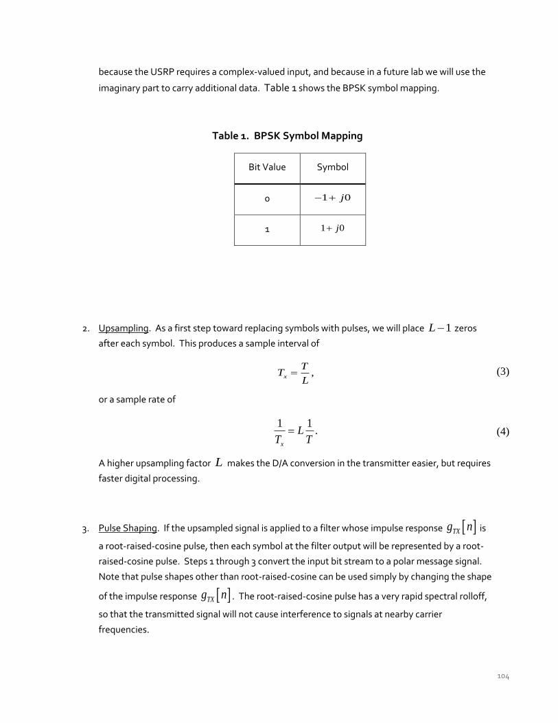
104
because the USRP requires a complex-valued input, and because in a future lab we will use the
imaginary part to carry additional data. Table 1 shows the BPSK symbol mapping.
Table 1. BPSK Symbol Mapping
Bit Value Symbol
0 1 0j
1 1 0j
2. Upsampling. As a first step toward replacing symbols with pulses, we will place 1L zeros
after each symbol. This produces a sample interval of
,x
TT
L (3)
or a sample rate of
1 1
.x
LT T
(4)
A higher upsampling factor L makes the D/A conversion in the transmitter easier, but requires
faster digital processing.
3. Pulse Shaping. If the upsampled signal is applied to a filter whose impulse response TXg n is
a root-raised-cosine pulse, then each symbol at the filter output will be represented by a root-
raised-cosine pulse. Steps 1 through 3 convert the input bit stream to a polar message signal.
Note that pulse shapes other than root-raised-cosine can be used simply by changing the shape
of the impulse response TXg n . The root-raised-cosine pulse has a very rapid spectral rolloff,
so that the transmitted signal will not cause interference to signals at nearby carrier
frequencies.

105
4. Modulation. The polar message signal, consisting of a train of pulses of the form
1 0 TXj g n , can be sent directly to the USRP transmitter. The USRP will convert the
signal to continuous time and add the carrier as shown in Eq. (2).
Receiver
A PSK receiver begins with a DSB-SC demodulator. When the transmitted BPSK signal arrives at
the receiver it has the form of a train of pulses, each given by
cos 2 ,TX cr t Dg t f t (5)
where D is a constant (usually much smaller than the constant A in the transmitted signal) and
the angle represents the difference in phase between the transmitter and receiver carrier
oscillators. If the receiver’s carrier oscillator is set to the same frequency as the transmitter’s carrier
oscillator, the USRP receiver will do most of the work in demodulating the BPSK signal. The
receiver’s Fetch Rx Data will provide a train of output pulses, each given by
.2
j
TX
Dr n g n e (6)
The sampling rate in Eq. (6), 1 zT , is set by the receiver’s “IQ rate” parameter. This rate is set to
provide M samples every T seconds, where 1 T is the symbol rate.
We can remove the phase offset using any one of a variety of techniques. The technique used in
the DSB-SC lab project works well. To summarize, we begin by squaring r n , giving
2
2 2 2 .4
j
TX
Dr n g n e (7)
This step eliminates phase changes caused by the data, as well as phase changes caused by
changes in the polarity of TXg n . Next, the angle 2 can be extracted using a Complex to Polar
function from the Data TypesNumericComplex palette. It turns out to be helpful at this point to
smooth variations in 2 caused by noise. The median filter from the ExternalFiles folder does a
good job. The default values can be accepted for the “left rank” and “right rank” parameters. Next
the Unwrap Phase from the AnalysisSignal ProcessingSignal Operations palette will remove

106
jumps of 2 . Finally, dividing by two gives the desired estimate of the phase error . The block
diagram in Figure 1 shows the entire phase synchronization process.
Figure 1. Carrier Phase Synchronization
The remaining steps carried out by the receiver should be familiar from the ASK and FSK labs.
These steps are:
1. Matched Filtering. We will use a root-raised-cosine receiver filter. This filter’s impulse response
RXg n is matched to the pulse shape TXg n of the received pulses. The matched filter gives
optimum performance in the presence of additive, white, Gaussian noise. Further, the cascade
of the two root-raised-cosine filters TXg n and RXg n produce a raised-cosine pulse shape
that is free from intersymbol interference.
2. Pulse Synchronization. The matched filter output is an analog baseband signal that must be
sampled once per symbol time, i.e. once every T seconds. Because of filtering, propagation
delays, and distortion caused by the communication channel, it is necessary to determine the
optimum time to take these samples. A function called PulseAlign(real) has been provided to
align the baseband signal so that the sample at index 0 is the correct first sample.
3. Sampling. The Decimate function will sample the aligned baseband waveform at index 0 and
every T seconds thereafter.
107
4. Detection. Once the baseband waveform has been sampled, each sample must be examined to
determine whether it represents a symbol of value 1 or a symbol of value 0.
5. Symbol Mapping. The detected symbol values must be converted to bits. For binary PSK, this
step is easily included in the detection step.
9.3 Pre-Lab
Transmitter
1. Create a program to generate a BPSK signal using the USRP. A template for the transmitter
has been provided in the file BPSKTxTemplate.gvi. This template contains the four functions
for interfacing with the USRP along with MT Generate Bits from the Modulation Toolkit. MT
Generate Bits will create a pseudorandom sequence of bits that can serve as a data sequence for
testing your BPSK system. Note that by default, MT Generate Bits will produce the same
sequence of bits every time you run the program. This is useful for debugging, but if you would
like to generate a different sequence of bits every time, wire a random number to the “seed in”
input. The steps below contain details about how to create the required transmitter.
2. First do the symbol mapping, as shown in Table 1.
3. Upsample the array of symbols using Upsample from the AnalysisSignal ProcessingSignal
Operation subpalette. In this lab project you are given control inputs to set the symbol rate
1 T and the IQ rate 1 xT . Set the symbol rate to 10,000 symbols/s and the IQ rate to
3200 10 Sa/s . Use the symbol rate and coerced IQ rate to calculate the upsampling factor L .
4. Use MT Generate Filter Coefficients from the Modulation Toolkit to generate the pulse shaping
filter. (MT Generate Filter Coefficients can be found on the Analysis

108
CommunicationsDigitalUtilities subpalette.) Set the modulation type to PSK, and the
pulse-shaping filter “samples per symbol” to your calculated value of L . Create a front-panel
control for “pulse shaping filter” and set this to “Root Raised.” Wire the “pulse shaping filter
coefficients” output to the “Y” input of a Convolution. The Convolution is available from the
AnalysisSignal ProcessingSignal Operation subpalette. Wire the output from your
upsampler to the “X” input of the Convolution.
5. Normalize the amplitude of your filtered message signal to a maximum absolute value of 1.
The Quick Scale 1D function in the ExternalFiles folder will find the maximum of the absolute
value. To ensure that your scaled message remains complex-valued, use a separate division
function to do the actual scaling. Connect the scaled message to the Build Waveform function
that connects to the Baseband Waveform graph provided in the template. Also send the scaled
message to the Write Tx Data function.
6. To observe the spectrum of the transmitted signal, wire the complex baseband waveform to
the FFT Power Spectrum function that connects to the Power Spectrum graph provided in the
template.
This completes construction of the BPSK transmitter. Save your transmitter in a file whose name
includes the letters “BPSKTx” and your initials (e.g. BPSKTx_BAB.gvi).
Receiver
1. Create a program to implement a BPSK receiver using the USRP. A template for the receiver
has been provided in the file BPSKRxTemplate.gvi. This template contains the six interface
functions for interfacing with the USRP.
Calculate the “number of samples” for the Fetch Rx Data function to fetch using the message
length, symbol rate front panel inputs and the coerced IQ rate. Double the number of samples
the receiver will fetch to acquire two frames of data. Since the receiver’s starting point is
random, this ensures that there will be one complete frame of received data in the block of
samples fetched.

109
Implement the carrier phase synchronization as shown in Figure 1.
2. To implement the receiver’s matched filter, use MT Generate Filter Coefficients just as you did
for the transmitter. Set the modulation type to PSK, and calculate the “matched samples per
symbol” M from the “actual IQ rate (1 zT )” and the symbol rate (1 T ) obtained from the
front-panel control. Create a front-panel control for “pulse shaping filter” and set this to “Root
Raised.” Wire the “matched filter coefficients” output to the “Y” input of a Convolution. The
output of your pulse shaping filter should be connected to the Cluster Properties function
provided in the template. The Cluster Properties function feeds the Baseband Output graph.
3. Place the PulseAlign (real) function from the ExternalFiles folder on your block diagram and wire
the baseband output waveform to the “input waveform” input and wire the M samples/symbol
to the “receiver sampling factor” input.
Once the baseband waveform is aligned, it can be sampled. The Decimate (single shot) function
can be obtained from the AnalysisSignal ProcessingSignal Operation subpalette. The
“decimating factor” is M .
4. The Modulation Toolkit function MT Format Eye Diagram has been provided in the receiver
template. Wire the baseband output waveform to the “waveform” eye-diagram input. The
“symbol rate (Hz)” input value is available from the front panel control. Set the “eye length”
parameter to 2.
5. To determine whether each received sample is more likely to represent a 1 or a 0, the sample
must be compared with a threshold. Because the message is a polar signal, the threshold can
be taken as zero. The result of this comparison is the receiver’s digital output. The output of
the comparison will be a Boolean array. You can convert this array to an integer array by using
a Boolean To Integer function.
This completes construction of the BPSK receiver. Save your receiver in a file whose name includes
the letters “BPSKRx” and your initials (e.g. BPSKRx_BAB.gvi).
110
Questions
1. In Transmitter Step 3 you are given 1 10,000 symbols/sT and 31 200 10 Sa/sxT . Find
the corresponding value for the number of samples per symbol L .
2. Eq. (6) in the Background section above shows that the received baseband signal r n includes
a factor je , where is any phase difference that may exist between the transmitter and
receiver carrier oscillators. Explain what would happen if you omitted the phase
synchronization step in the receiver. Specifically, what would be the receiver output if just
happened to take the value 2 ?
3. In Receiver Step 2 the “actual IQ rate” 1 zT may be different from the rate 1 xT that was used at
the transmitter. ( Note that the symbol rate 1 T must be the same at the transmitter and
receiver.) The value of the receiver’s IQ rate determines the receiver sampling factor M . What
is the advantage to using a higher value of M ? What is the advantage of using a lower value of
M ?
4. Although BPSK is a suppressed-carrier version of ASK, we do not use an envelope detector to
demodulate BPSK the way we did for ASK. Why is that? What would the receiver output be if
we used an envelope detector for demodulation?
5. Bit error rate is a measure of performance of a digital communication system. What would the
bit error rate be if the transmitter failed and the receiver received only noise? Explain your
reasoning.
9.4 Lab Procedure 1. Connect a loopback cable and attenuator between the TX 1 and RX 2 connectors of the USRP.
Connect the USRP to your computer and plug in the power to the USRP. Run LabVIEW and
open the transmitter that you created in the prelab.
111
2. Ensure that the transmitter is set up to use
Carrier Frequency: 915.0 MHz
IQ Rate: 200 kHz. Note: This sets the value of 1 xT .
Gain: 0 dB.
Active Antenna: TX1
Symbol rate: 10,000 symbols/s
Message Length: 1000 bits
Pulse shaping filter: Root Raised
Run the transmitter. Use the large STOP button on the front panel to stop transmission
connectors.
3. After running the transmitter, observe the spectrum of the transmitted signal. Measure the
“main lobe” bandwidth of the transmitted signal. Change the pulse shaping filter control to
“none” to create rectangular pulses and run the transmitter again. Compare the spectrum of
the transmitted signal with the spectrum for root-raised-cosine pulses. Return the pulse
shaping filter control setting to “Root Raised.”
4. Ensure that the receiver is set up to use
Carrier Frequency: 915.0 MHz
IQ Rate: 200 kHz. Note: This sets the value of 1 zT .
Gain: 0 dB
Active Antenna: RX2
Symbol rate: 10,000 symbols/s
Message Length: 1000 bits
Pulse shaping filter: Root Raised

112
5. Run the transmitter, then run the receiver. Once the receiver has acquired a block of data, you
may stop the transmitter.
6. Observe the eye diagram. Make note of the optimum sampling time and the presence or
absence of intersymbol interference. To see the effect of pulse synchronization, move the
waveform input of MT Format Eye Diagram to the “aligned waveform” output of
PulseAlign(real). Run the transmitter and receiver again. Observe the eye diagram. What is the
optimum sampling time now?
113
7. Modify the transmitter to include the AddFrameHeader(real), available in the BasicUSRPLabs
folder. Place AddFrameHeader(real) after the symbol mapping, but before conversion of the
symbols to complex. Next, modify the receiver to include the FrameSync(real), also available
from the BasicUSRPLabs folder. Place FrameSync(real) immediately following Decimate. Wire
the output of Decimate to the “Sampled Input” of FrameSync(real). Leave the remaining inputs
of FrameSync(real) unwired. Wire the “Aligned Samples” output of FrameSync(real) to the
threshold comparison function.
Wire the array of output bits from the threshold comparison to the “array” input of an Array
Subset function. Set the “index” input to zero, and set the “length” input to the length specified
by the “message length” control. Display the output of Array Subset function as “Output bits”
on the receiver front panel.
Note that the “Output Signal” and “max index” outputs of FrameSync(real) will not be used in
this lab project.
8. Automate measurement of the bit error rate (BER) by using the MT Calculate BER from the
Modulation Toolkit (Analysis CommunicationsDigitalMeasurements subpalette). From
the Configure ribbon, choose “PN Fibonacci.” Set the “BER trigger threshold” to 0.4. Connect
indicators to the “BER” and “trigger found?” outputs. When you run the program, “trigger
found?” will be true whenever the measured BER is below the BER trigger threshold.
Run the transmitter and receiver. If everything is working correctly, the BER should be 0 or 1.0.
Run the transmitter and then run the receiver a dozen times or so. Verify that about half the
time the BER is 0 and about half the time the BER is 1.0.
Questions
1. How do the main lobe bandwidth and spectral rolloff rate for root-raised cosine pulses compare
with the same quantities when rectangular pulses are used?
2. What does a BER of 1.0 signify? Explain why the BER is 0 half the time and 1.0 half the time.
114
Differential Encoding
Suppose the data bits are passed through the logic circuit shown in Figure 2 before being sent to
the transmitter. In this circuit, the exclusive-nor gate will produce a 0 whenever the current input
differs from the previous output, and a 1 whenever the current input is the same as the previous
output.
Q
QSET
CLR
D
Figure 2. Differential Encoder
For example, an input of
1 0 1 1 0 0 0 1
produces an output of
0 0 1 1 1 0 1 0 0 ,
assuming that the flip-flop has an initial state of 0. Now suppose that the received bit sequence is
passed through the circuit shown in Figure 3. The output will be a 1 whenever the current
Q
QSET
CLR
D
Figure 3. Differential Decoder
input and the previous input are the same, and the output will be a 0 whenever the current input
and the previous input are different. For example, a received bit sequence of
0 0 1 1 1 0 1 0 0
produces an output of
1 0 1 1 0 0 0 1 .
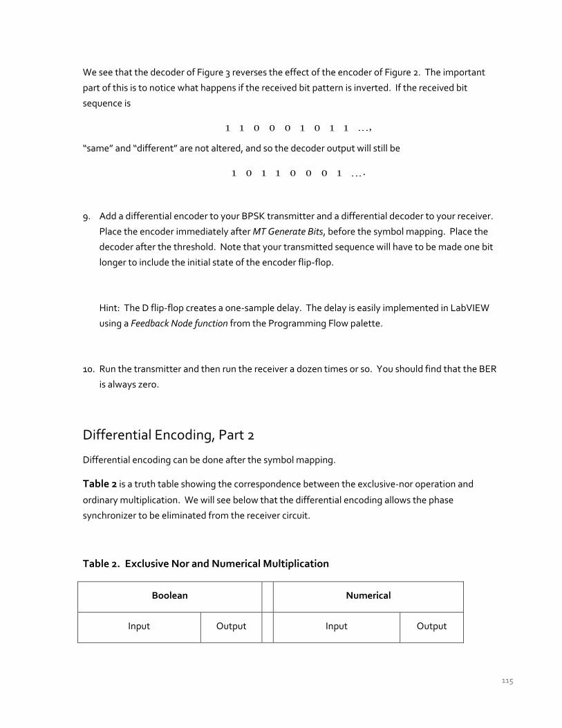
115
We see that the decoder of Figure 3 reverses the effect of the encoder of Figure 2. The important
part of this is to notice what happens if the received bit pattern is inverted. If the received bit
sequence is
1 1 0 0 0 1 0 1 1 ,
“same” and “different” are not altered, and so the decoder output will still be
1 0 1 1 0 0 0 1 .
9. Add a differential encoder to your BPSK transmitter and a differential decoder to your receiver.
Place the encoder immediately after MT Generate Bits, before the symbol mapping. Place the
decoder after the threshold. Note that your transmitted sequence will have to be made one bit
longer to include the initial state of the encoder flip-flop.
Hint: The D flip-flop creates a one-sample delay. The delay is easily implemented in LabVIEW
using a Feedback Node function from the Programming Flow palette.
10. Run the transmitter and then run the receiver a dozen times or so. You should find that the BER
is always zero.
Differential Encoding, Part 2
Differential encoding can be done after the symbol mapping.
Table 2 is a truth table showing the correspondence between the exclusive-nor operation and
ordinary multiplication. We will see below that the differential encoding allows the phase
synchronizer to be eliminated from the receiver circuit.
Table 2. Exclusive Nor and Numerical Multiplication
Boolean Numerical
Input Output Input Output
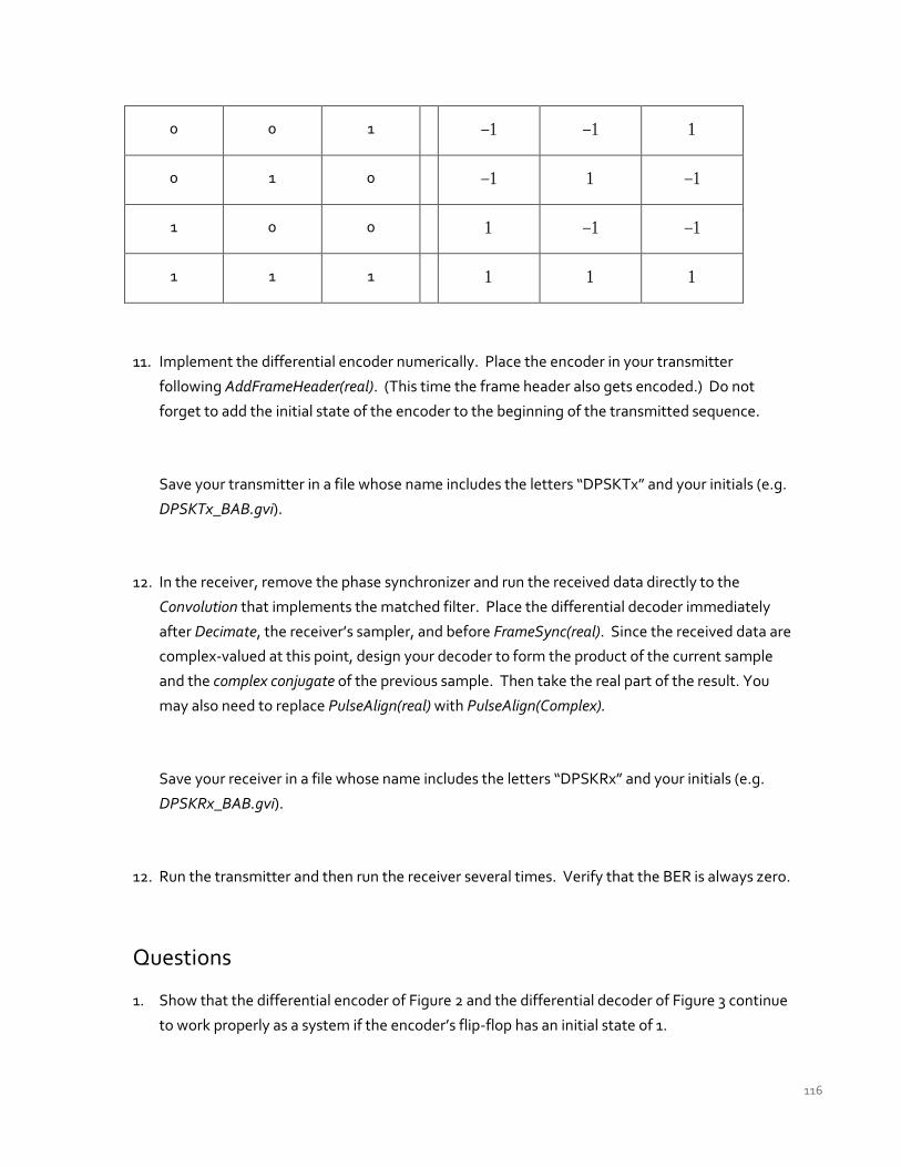
116
0 0 1 1 1 1
0 1 0 1 1 1
1 0 0 1 1 1
1 1 1 1 1 1
11. Implement the differential encoder numerically. Place the encoder in your transmitter
following AddFrameHeader(real). (This time the frame header also gets encoded.) Do not
forget to add the initial state of the encoder to the beginning of the transmitted sequence.
Save your transmitter in a file whose name includes the letters “DPSKTx” and your initials (e.g.
DPSKTx_BAB.gvi).
12. In the receiver, remove the phase synchronizer and run the received data directly to the
Convolution that implements the matched filter. Place the differential decoder immediately
after Decimate, the receiver’s sampler, and before FrameSync(real). Since the received data are
complex-valued at this point, design your decoder to form the product of the current sample
and the complex conjugate of the previous sample. Then take the real part of the result. You
may also need to replace PulseAlign(real) with PulseAlign(Complex).
Save your receiver in a file whose name includes the letters “DPSKRx” and your initials (e.g.
DPSKRx_BAB.gvi).
12. Run the transmitter and then run the receiver several times. Verify that the BER is always zero.
Questions
1. Show that the differential encoder of Figure 2 and the differential decoder of Figure 3 continue
to work properly as a system if the encoder’s flip-flop has an initial state of 1.

117
2. Show, starting with Eq. (6), why the phase synchronizer is not needed in the DPSK receiver.
3. In the BPSK system, the eye diagram has the same amplitude every time you run the receiver.
In the DPSK system, the amplitude of the eye diagram changes on every run. Explain why this
happens. Explain whether, if noise were present, the BER would also change every time the
DPSK receiver is run.
4. Differential phase-shift keying is intended to be robust in the presence of a phase difference
between the transmitter and receiver oscillators. It is also possible for there to be a frequency
difference between the oscillators. Suppose there is a small frequency difference of f
between the transmitter and receiver oscillators. Modify Eq. (6) to take this frequency
difference into account. How will the output of the DPSK receiver change because of this
frequency difference? Using the parameter values of this lab project, determine how large a
frequency difference will be “significant.” Be sure to specify what you mean by “significant.”
9.5 Report
Prelab
Hand in documentation for the programs you created for the transmitter and receiver. Also include
documentation for any functions you created. To obtain documentation, print out legible
screenshots of the front panel and block diagram.
Answer all of the questions in the Prelab section marked Questions.
Lab
Submit the program you created for the transmitter and receiver. Include both the BPSK and DPSK
programs. Also submit any functions you created. Be sure your files adhere to the naming
convention described in the instructions above.

118
Submit documentation for the DPSKTx and DPSKRx programs. Resubmit documentation for any
functions you modified during the lab.
Answer all of the questions in each of the Lab Procedure sections marked Questions above.

119
L A B 1 0
The Eye Diagram
120
Prerequisite: Lab 9 – Binary Phase-Shift Keying (BPSK)
10.1 Objective Although we have displayed an eye diagram in each of the digital labs so far, we have relied on the
Modulation Toolkit to produce the display. In this lab project we will learn how to create an eye
diagram from scratch. We will examine how the eye diagram changes when intersymbol
interference (ISI) is present in the communication channel, and we will learn how to make
quantitative measurements of the amount of ISI from the eye diagram.
In this lab project you will use the BPSK transmitter and receiver that you created for Lab 9 as a
“test bed” system. To create ISI, a function called Channel.gvi has been provided. If a second USRP
is available, however, you can try transmitting from one USRP to the other using antennas to see
how much ISI is actually present owing to multipath propagation in your own physical environment.
10.2 Background Viewed as a complex baseband signal, the waveform generated by the BPSK transmitter can be
written
,n TX
n
x t A a g t nT
(1)
where A is a constant that sets the transmitted average power, 1na are the symbol values
carrying the transmitted information, TXg t is the transmitted pulse shape, and T is the time
between symbols. The tilde over the x signifies that this is the baseband signal; the actual
transmitted signal is
2Re
cos 2 .
cj f t
n TX c
n
x t x t e
A a g t nT f t
(2)
121
Note that the pulse TXg t is assumed to be real valued.9
The transmitted signal passes through the communication channel and then is demodulated by the
receiver. Let us model the communication channel as a linear time-invariant filter having baseband
impulse response h t . When the signal arrives at the receiver and is demodulated, it is passed
through the receiver filter having impulse response RXg t . Let us designate the impulse response
of the cascade of the transmitter filter, the channel, and the receiver filter as g t . That is,
.TX RXg t g t h t g t (3)
The cascade of TXg t and RXg t is usually designed to be free of ISI. In this lab project we will
use a cascade in which the combined filter has a raised-cosine spectral shape for that purpose.
Unfortunately, the channel response h t is not under the designer’s control, and may contribute
ISI to the received signal. After filtering at the receiver, the received signal can be written
,k
n
y t D a g t nT n t
(4)
where D is an amplitude constant, g t is the pulse shape given by Eq. (3), and n t is white
Gaussian noise that has been passed through the receiver filter.
Once the received signal has been filtered, it is sampled, at the rate of one sample every T
seconds. Assuming that pulse synchronization has been applied, so that the samples are taken at
the correct times, the sampled signal is
.n
n
y kT D a g k n T n kT
(5)
These samples are compared with a threshold of zero to decide whether each received symbol is
most likely to represent a 1 or a 1 . Let us rewrite Eq. (5) as
9 The signal x t and the impulse responses
TXg t and
RXg t are all actually implemented in discrete time.
Writing these as continuous time functions makes the discussion much easier to read, however.

122
0 .k n
nn k
y kT Da g D a g k n T n kT
(6)
The first term in Eq. (6) represents the desired sample at time t kT , the second term represents
ISI, and the third term represents noise.
To get a sense of how much ISI a given g t might produce in the worst case, let us suppose that
1ka and ,na n k , forms a pattern that makes every ISI term negative. That is, suppose the data
pattern is
1, 0
1, 0.n
g k n Ta
g k n T
(7)
Then Eq. (6) becomes
0
0
0 .
nn k
n
y kT Dg D g k n T n kT
Dg D g nT n kT
(8)
Ignoring noise, the sample given by Eq. (8) represents a “worst case” value. We write
0
0 .w
n
V Dg D g nT
(9)
We can also identify a “best case” sample value. If every ISI term enhances the desired sample we
have
0
0 .b
n
V Dg D g nT
(10)
Traditionally, the quantity of ISI present at the output of the receiver filter is measured by either of
two parameters. The peak distortion is defined as
0peak distortion .
0n
D g nT
Dg
(11)
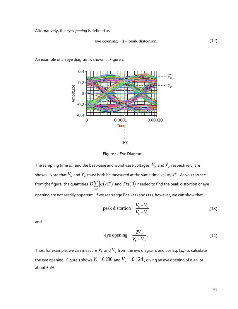
123
Alternatively, the eye opening is defined as
eye opening 1 peak distortion. (12)
An example of an eye diagram is shown in Figure 1.
Figure 1. Eye Diagram
The sampling time kT and the best-case and worst-case voltages, bV and wV respectively, are
shown. Note that bV and wV must both be measured at the same time value, kT . As you can see
from the figure, the quantities 0n
D g nT
and 0Dg needed to find the peak distortion or eye
opening are not readily apparent. If we rearrange Eqs. (11) and (12), however, we can show that
peak distortion b w
b w
V V
V V
(13)
and
2
eye opening .w
b w
V
V V
(14)
Thus, for example, we can measure bV and wV from the eye diagram, and use Eq. (14) to calculate
the eye opening. Figure 1 shows 0.296bV and 0.124wV , giving an eye opening of 0.59, or
about 60%.

124
Intersymbol interference is of concern because it degrades the performance of the communication
system. For a BPSK system using a matched receiver filter with additive white Gaussian noise and
no ISI, the probability of error is given by
0
2,b
e
EP Q
N
(15)
where bE is the average energy per bit at the receiver, 0 2N is the power spectrum of the noise at
the receiver input, and Q is the Gaussian probability integral. If ISI is present, the probability of
error is dominated by the worst-case situation. For an eye opening the worst-case probability of
error is given by
0
2,b
e
EP Q
N
(16)
where bE is the energy per bit without including ISI, as in Eq. (15).
10.3 Pre-Lab
Eye Diagram
1. Modify your BPSK receiver to include your own eye diagram functionality. Here is how:
The required eye diagram is a plot of the aligned waveform at the output of PulseAlign(real).
The horizontal (time) axis has a duration of two symbol times. The plots corresponding to
successive pairs of symbols are overlapped. To make such a plot, extract the Y-array from the
aligned waveform. Also extract dt ; you will need it as described below. Then use the Reshape
Array function from the Data TypesArray subpalette to form a two-dimensional array for
which each row contains two symbols of data. In the Reshape Array function, the first
“dimension size” input is the number of rows and the second “dimension size” input is the
number of columns. The number of rows is the number of curves to plot, and the number of
columns is the number of samples in two symbols of data. You will need to calculate these
numbers in your program. The output of Reshape Array function is a two dimensional array,
which must be connected to the “2D DBL to 1D Cluster” function before it is ready for plotting.
Use your value of dt , and the output of Reshape Array function. Connect the resulting cluster
to a Waveform Graph indicator. When the Waveform Graph indicator is given a two dimensional

125
array to plot, it plots each row of the array as a separate curve. This is exactly the behavior that
you want to produce the eye diagram.
2. Save your modified BPSK receiver in a file whose name includes the letters “BPSKEyeRx” and
your initials (e.g. BPSKEyeRx_BAB.gvi).
Channel Model
To test your eye diagram, you will need to introduce some ISI. Channel.gvi, in the BasicUSRPLabs
folder is provided for the purpose. Add Channel.gvi immediately after Fetch Rx Data in your
receiver. Connect the “Use Channel” and “Propagation Delay” inputs to front panel controls.
Connect the “Samples per Symbol” input to the samples per symbol calculated from the actual IQ
rate and the symbol rate in your receiver. You may leave the other inputs of Channel.gvi
unconnected.
Channel.gvi simulates a multipath channel. The default channel parameters create an impulse
response given by
0.2 0.08 2 ,h t t t t (17)
where is the “propagation delay” set by the front panel control. Channel.gvi can also add noise
to the signal, but we will not be using this feature in this lab project.
Multipath propagation tends to create peaks and dips in the frequency response of the
communication channel. This creates the distortion of the received signal that leads to intersymbol
interference. Some authors use the so-called coherence bandwidth as a measure of the irregularity
of the channel frequency response. Roughly, the coherence bandwidth is the frequency interval
over which the gain of the channel remains approximately constant. Intersymbol interference will
become serious when the signal bandwidth exceeds the coherence bandwidth of the channel.
Coherence bandwidth is inversely related to the spread in propagation delays between the first-
arriving and last-arriving signal. For the default channel of Eq. (17), the coherence bandwidth is
inversely proportional to the parameter . The relation is
0.816
,cohB
(9.1)
126
where cohB is the coherence bandwidth in Hz when is in seconds.
Questions
1. Use Eq. (15) to find 0bE N for a probability of error of 610eP . Now use Eq. (16) to find eP
for an eye opening of 0.8 . Repeat for 0.5 . Using the same 0bE N , find the value of
eye opening that will give 510eP .
2. Suppose 0 1g , 0.2g T , 2 0.08g T , and 0g nT otherwise. Use Eqs. (9)
and (10) to find wV and bV . Then use Eq. (14) to find the eye opening.
3. Using Eq. (18), find the coherence bandwidth for 50 s , 100 s , and 150 s .
10.4 Lab Procedure 1. Connect a loopback cable and attenuator between the TX 1 and RX 2 connectors of the USRP.
Connect the USRP to your computer and plug in the power to the USRP. Run LabVIEW and
open the transmitter that you created in the prelab.
2. Ensure that the transmitter is set up to use
Carrier Frequency: 915.0 MHz
IQ Rate: 200 kHz. Note: This sets the value of 1 xT .
Gain: 0 dB
Active Antenna: TX1
Symbol rate: 10,000 symbols/s
Message Length: 1000 bits
Pulse shaping filter: Root Raised
Run the transmitter. Use the large STOP button on the front panel to stop transmission
connectors.
127
3. After running the transmitter, observe the spectrum of the transmitted signal. Measure the
“main lobe” bandwidth of the transmitted signal. The baseband signal bandwidth is half of the
main lobe bandwidth, counting only the positive-frequency components.
4. Ensure that the receiver is set up to use
Carrier Frequency: 915.0 MHz
IQ Rate: 200 kHz. Note: This sets the value of 1 zT . Note that zT is the same parameter as dt
.
Gain: 0 dB
Active Antenna: RX2
Symbol rate: 10,000 symbols/s
Message Length: 1000 bits
Pulse shaping filter: Root Raised
Use Channel: off
5. Run the transmitter, then run the receiver. Once the receiver has acquired its data, you may
stop the transmitter. The receiver should show a BER of 0.0 or 1.0. Do not be concerned about
a BER of 1.0 in this lab project.
6. Observe the eye diagram created by the program you created in step 1 of the prelab. Measure
wV and bV and calculate the eye opening. Owing to filtering in the USRP, the eye opening
should not be 100%.
The most effective way to measure wV and bV from the eye diagram is to use cursors. Click on
the eye diagram graph and in the ribbon, click the Graph Parts button. In the dialog window,
click the Cursor Legend enable icon. To create a new cursor, click the New Cursor button in the
Cursors dialog next to the Eye diagram.
To measure wV and bV , place the X cursor at a time at which the eye opening is widest. This
will be near the center of the time axis. Then use the Y cursor to measure wV and bV . Do not
move the X position between measurements. You will get a more accurate pair of measurements if you zoom in on the relevant part of the eye diagram before positioning the Y cursor. (Graph Parts button, Graph Tools)

128
7. Set the propagation delay to 50 s , set Use Channel to “on,” and repeat steps 5 and 6.
Repeat for 100 s and 150 s . Prepare a table showing the eye opening for each
value of .
Questions
1. Why in this lab project are we not concerned if the BER turns out to be 1.0?
2. Multipath propagation is common in the cellular telephone environment. Propagation delays
can vary depending on the locations of the base station, the mobile unit, and nearby buildings,
but these delays do not depend on symbol rate. However, with each new generation of cellular
service the symbol rate increases. Based on your findings in this lab project, discuss the
relationship between symbol rate, coherence bandwidth, eye opening, and BER. What
happens as the symbol rate increases?
10.5 Report
Prelab
Hand in documentation for your modified receiver including the eye diagram. Also include
documentation for any functions you created. To obtain documentation, print out legible
screenshots of the front panel and block diagram.
Answer all of the questions in the Prelab section marked Questions.
Lab
Submit the modified receiver including the eye diagram. Resubmit documentation for any
functions you modified during the lab. Submit the table required in Lab Procedure step 7 above.
Answer the questions in the Lab Procedure section marked Questions.

129
L A B 1 1
Equalization
130
Prerequisite: Lab 10 – The Eye Diagram
11.1 Objective In most digital communication systems, the transmitter’s pulse shaping filter and the receiver’s
matched filter are designed so that the pulses that emerge from the receiver’s matched filter do not
exhibit any intersymbol interference. As we discussed in the eye diagram lab project, however, the
communication channel often introduces additional filtering that can result in intersymbol
interference.
One way to deal with intersymbol interference created by the communication channel is to add an
additional filter in the receiver. Ideally, this new filter will have a response that is “inverse” to the
filtering caused by the channel. A filter intended to counter the adverse effects of channel filtering
is called an equalizer.
In wireless systems, the channel distortion is often caused by multipath propagation. That is, the
received signal may include reflections from buildings and other objects in the environment. The
distortion that is observed in any particular wireless link will depend on the location of the
transmitter, the location of the receiver, and the locations of nearby reflecting objects. Since the
transmitter, the receiver, and even some of the reflecting object can move, channel distortion can
change gradually with time. In this kind of application it is helpful to have an equalizer that is
adaptive; that is, we would like the equalizer to be able to change its properties slowly with time to
follow changes in the channel.
In this lab project you will use the BPSK transmitter and receiver that you created for Lab 9 as a
“test bed” system. The Channel.gvi that you used in the eye diagram lab project will create the
intersymbol interference. The equalizer that we will investigate is provided in the Modulation
Toolkit.
11.2 Background Equalizers, particularly adaptive equalizers, are nearly always implemented as FIR filters. There are
two reasons for this. First, and most important, an FIR filter is always stable. As a result, we do not
131
have to be concerned that the equalizer might become unstable as it adapts. Second, it sometimes
turns out that the “optimum” equalizer is not causal. A non-causal FIR filter can always be made
causal by adding a finite delay. This easy fix cannot be applied to a non-causal IIR filter.
Experience shows that it is often possible to model the communication channel as an FIR filter as
well. In a multipath environment successive reflections become weaker, and eventually drop below
the noise floor. Commonly, only a few of the strongest reflections are significant causes of ISI.
Unfortunately, the inverse of an FIR filter is always an IIR filter, and this means that an FIR equalizer
will never be able to completely remove the ISI caused by an FIR channel. We will find that even a
very long FIR equalizer always leaves a small amount of residual ISI.
Suppose that y k y kT represents the sampled output of the receiver’s matched filter. The
parameter T represents the time between samples and also the time between transmitted
symbols. Recall from the eye diagram lab project that each sample y k is the sum of a desired
sample value, ISI, and noise. The block diagram representation of an FIR equalizer is shown in
Figure 1.

132
Figure 1. An FIR Equalizer
The output of the equalizer is denoted as z k . In the diagram, blocks designated 1z represent
one-sample delay elements. Arrows leading to multiplication by coefficients nc are traditionally
known as “taps,” and the coefficients themselves are known as “tap gains.” This block diagram
represents the equation
.N
n
n N
z k c y k n
(1)

133
Our goal in designing an equalizer is to find values for the tap gains , ,N Nc c that will minimize
any residual ISI. Even better, we would like to find a way to have the tap gains adjust themselves to
reduce ISI as the equalizer runs.
To provide a basis for adjusting the equalizer tap gains , ,N Nc c , the receiver must know what
data the transmitter is sending. Common practice is to begin transmission with a “training
sequence” , 0, , 1k tb k N that is known to the receiver. In this lab project we will use the
same 26-symbol sequence that we are already using for frame synchronization. It is assumed that
once the 26tN symbol training sequence has been received, the tap gains will have had time to
adjust themselves to nearly their optimum values. Thus from this time on, the sequence z k
should be nearly ISI-free. Following the equalizer, the BPSK receiver performs detection and
symbol mapping by comparing z k with a threshold of zero. If ˆkb represents the output data,
then
1, if 0ˆ
0, if 0.k
z kb
z k
(2)
What will the receiver use as a basis for adjusting the equalizer tap gains once the training sequence
is complete? In a decision-directed equalizer, the decisions ˆkb are used to replace the training
sequence bits kb . Even when the probability of error is relatively high (e.g. 0.01), the decisions ˆkb
are hardly ever wrong. It turns out that an occasional incorrect tap gain adjustment causes little
change in the ISI output of the equalizer. Figure 2 shows the organization of the decision-directed
equalizer.

134
Equalizer
Adjust Tap
Gains
Switch when
training sequence
ends
Figure 2. Decision-Directed Equalizer
There are a number of alternative criteria for deciding when the equalizer tap gains are optimally
adjusted. One possibility is to adjust the tap gains to maximize the eye opening. It turns out,
however, that equalizers have a tendency to amplify the noise that forms part of the input
sequence y k . Maximizing the eye opening also tends to enhance the noise. An alternative
criterion minimizes the mean squared error between the sequence z k and the symbol sequence
ka based on kb . Since the mean squared error includes both ISI and noise, this criterion is less
prone to noise enhancement than methods that ignore noise. Now if ka is the symbol sequence
corresponding to the training sequence bits kb , we can write the mean squared error E as
2
,kE z k a E (3)
where E is the expectation operator. Substituting Eq. (1) gives
2
.N
n k
n N
E c x k a
E (4)
If we were designing a fixed equalizer, we would find the tap gains , ,N Nc c that minimize E in
Eq. (4). Instead, we want to find a way to let the tap gains adjust themselves. Suppose
, ,
q q
N Nc c represent the values of the tap gains after the q -th update. We can further update the
tap gains according to the algorithm
1 , , , , 0,1, .q q
n n
n
c c n N N qc
E (5)

135
This algorithm is an example of a steepest descent procedure, as it moves the coefficients in the
direction of the negative of the gradient of the mean-squared error with respect to the coefficient
values. This is the direction of the steepest descent down the slope to the minimum of the mean-
squared error. The parameter adjusts the step size. We can evaluate the derivative nc E by
using Eq. (4):
2
2
2 , , , ,
N
i k
i Nn
k
E c y k i a y k nc
E z k a y k n
E e k y k n n N N
E
(6)
where ke k z k a is the error signal (including both noise and ISI) at index k .
It turns out that the expectation operator in Eq. (6) poses something of a problem, since there is no
way to evaluate it in an actual filter implementation. We can avoid the problem by approximating
the expectation by the current value. That is,
.E e k y k n e k y k n (7)
Then the rule for updating the tap gains becomes
1 y , , , , 0,1, .q q
n nc c e k k n n N N q (8)
Normally we will update the equalizer tap gains after every received symbol. Thus the index k and
the index q increment together. We have
1 y , , , , 0,1, .k k
n nc c e k k n n N N k (9)
The procedure expressed by Eq. (9) is called the least mean square (LMS) algorithm for adjusting the
equalizer tap gains. We initialize the procedure by taking
1, 0
0, otherwise.n
nc
(10)
A block diagram of the LMS adaptive equalizer is shown in Figure 3.

136
Symbol
Mapping
Figure 3. LMS Adaptive Equalizer
Note in Eq. (9) that if the step size is small, the tap gain values will never change very much on a
single update. This means that the tap gain values at any time are the accumulated sums of many
small adjustments. Since accumulation is a form of averaging, Eq. (9) justifies our approximating
the expectation operator by a single sample in Eq. (7). Further, since the tap gains change very little
each time they are adjusted, a single symbol error does not push the equalizer very far out of
adjustment when decision feedback is in use.
137
11.3 Pre-Lab 1. For this lab project you will use the BPSK transmitter and receiver you created for the phase-
shift keying lab project. Be sure your receiver includes the Channel.gvi containing the channel
model, and also includes the capability of displaying an eye diagram. You may use either MT
Format Eye Diagram from the Modulation Toolkit, or the eye diagram program that you created
for the eye diagram lab project. Wire the “ISI Channel Model” Channel.gvi input to a front panel
control on your receiver.
2. Create a program to perform adaptive equalization. A template EqualizerTemplate.gvi has been
provided to get you started. The inputs to your equalizer are to be connected as follows:
a. Input Complex Waveform input to Equalizer.gvi will be connected to Output Complex Waveform on the FrameSync(real). This waveform has been aligned to the start of the frame, but has not been downsampled. This waveform also includes the received header symbols that will be used to train the equalizer.
b. Receiver Sampling Factor input to Equalizer will be connected to the number of samples per symbol parameter that is calculated in your BPSK receiver.
c. Equalizer Length input to Equalizer should be connected to a control on your receiver front panel.
In addition to the inputs and outputs, the equalizer template contains a copy of the training
sequence, an array containing the symbol map, and a cluster of “feedforward equalizer
parameters.” These parameters include the number of equalizer taps per symbol (one), and the
values of step size to use during training and during decision-directed operation (0.05 during
training, 0.001 in decision-directed mode).
To complete the equalizer, you will need to add two functions from the Modulation Toolkit. These
are MT Generate System Parameters from the AnalysisCommunicationsDigitalUtilities
subpalette and MT PSK Feedforward Equalizer from the
AnalysisCommunicationsDigitalEqualization subpalette.
Click on the MT PSK Feedfordward Equalizer function then, from the Configure ribbon, choose
PSK(M) for the MT Generate System Parameters. Create a constant at the “PSK type” input and
select “Normal.” Wire your “Receiver Sampling Factor” to the “samples per symbol” input. Wire a
constant of value 2 to the “M-PSK” input. The only output of the MT Generate System Parameters
that you will use is the “PSK system parameters” cluster. Wire this to the Cluster Properties function
provided in the template to replace the default symbol map with the symbol map provided. The
modified PSK system parameters cluster will be used by the MT PSK Feedforward Equalizer.
138
From the Configure ribbon, choose Specify Length for the MT PSK Feedforward Equalizer.gvi. Wire
up the “input complex waveform” and “PSK system parameters” inputs. Wire the “equalizer
length” input to the appropriate control. Wire the “training bits” input to the training bits array
provided in the template. Wire “feedforward equalizer (LMS) parameters” to the cluster provided
in the template. The “reset” input can be left unwired, since it will default to the correct value of
“true.” Wire all of the outputs to the appropriate indicators and you are ready to go.
3. Save your equalizer in a file whose name includes the letters “Equalizer” and your initials (e.g.
Equalizer_BAB.gvi).
4. Open the block diagram of your BPSK receiver. Wire up the remaining inputs of FrameSync(real); that is, connect the “Input Signal” input to the “Aligned Signal” output of PulseAlign(real) and connect the “Receiver Sampling Factor” input to an appropriate location. The “Sampled Input” FrameSync(real) input should remain connected to the output of Decimate.
5. Add your equalizer to your BPSK receiver. Wire the inputs as described in Step 2 above. During
the lab you will be asked to take data to compare the eye diagrams before and after equalization. Wire the “Equalized Complex Waveform” equalizer output to a second eye diagram display. Also, wire the “Squared Error” output to a waveform graph indicator so that you will be able to observe the error decrease as the equalizer adapts. Wire the “Output Bits” and “equalizer coefficients out” outputs to indicators.
Questions
1. The default impulse response provided by Channel.gvi when the propagation delay is set at
100 s is 0.2 1 0.08 2h n n n n . Taking the z-transform gives channel
system function 1 21 0.2 0.08H z z z . An ideal equalizer will have a system function
that is the reciprocal of the channel system function. That is,
1 2
1
1 0.2 0.08eqH z
z z
. (11)
Find an expression for the ideal equalizer impulse response eqh n . The coefficients of
eqh n are the tap gains of an ideal (i.e. infinite length) equalizer. Find numerical values for
the first five tap gains 0 4, ,c c .
2. You should find that the ideal equalizer in Question 1 has a causal impulse response. The
equalizer of Figure 3 can be non causal, if necessary. As a non-causal example, repeat Question
1 for 0.1 1 0.3 2h n n n n . Find numerical values for 4 4, ,c c . (Hint: The
ideal equalizer is an IIR filter. While it need not be causal, it must be stable.)
139
11.4 Lab Procedure 1. Connect a loopback cable and attenuator between the TX 1 and RX 2 connectors of the USRP.
Connect the USRP to your computer and plug in the power to the USRP. Run LabVIEW and
open the transmitter that you created in the prelab.
2. Ensure that the transmitter is set up to use
Carrier Frequency: 915.0 MHz
IQ Rate: 200 kHz. Note: This sets the value of 1 xT .
Gain: 0 dB
Active Antenna: TX1
Symbol rate: 10,000 symbols/s
Message Length: 1000 bits
Pulse shaping filter: Root Raised
Run the transmitter. Use the large STOP button on the front panel to stop transmission
connectors.
3. Ensure that the receiver is set up to use
Carrier Frequency: 915.0 MHz
IQ Rate: 200 kHz. Note: This sets the value of 1 zT . Note that zT is the same parameter as dt
.
Gain: 0 dB
Active Antenna: RX2
Symbol rate: 10,000 symbols/s
Message Length: 1000 bits

140
Pulse shaping filter: Root Raised
Use Channel: off
4. Run the transmitter, then run the receiver. Once the receiver has acquired its data, you may
stop the transmitter. The receiver should show a BER of 0.0 or 1.0. Do not be concerned about
a BER of 1.0 in this lab project.
5. Set the channel model for a propagation delay of 100 s with the default channel model. Set
Use Channel to “on.” Set the “Equalizer Length” to 11. Run the transmitter and then the
receiver. Once the receiver has acquired data, you may stop the transmitter. Compare the eye
diagrams before and after equalization. Use cursors to measure wV and bV and calculate the
eye opening for each case.
6. Repeat Step 5 for propagation delays of 50 s and 150 s . Compare the eye opening before
and after equalization for each case. Prepare a table showing eye opening before and after
equalization for each of the three propagation delays.
7. Set the propagation delay of the channel back to 100 s and run the transmitter and receiver.
Observe the “Squared Error” equalizer output. Approximately what value does the squared
error reach in steady state?
8. At a propagation delay of 100 s and an equalizer length of 11, record the values of tap gains
4 4, ,c c . Compare with the values you computed in Prelab Question 1. (Do not expect
extremely close agreement. The prelab calculations were for an infinite-length equalizer.
Further, the adaptive equalizer tap gains are constantly being adjusted around their optimal
values. Try running the receiver a few times to see how much variation there is in the steady-
state tap gains.)
9. Change the ISI channel model to the model given in Prelab Question 2. Keep the propagation
delay at 100 s and the equalizer length at 11. Run the transmitter and receiver. Check the
141
eye diagrams to verify that the equalizer is working. Record the values of tap gains 4 4, ,c c .
Compare with the values you computed in Prelab Question 2.
10. With the propagation delay set at 100 s and using either of the two channel models, measure
the eye opening after equalization as the equalizer length is increased in odd-numbered steps
from 1. At what equalizer length does the eye opening stabilize?
11. Phase Synchronization Revisited. You may recall from the BPSK lab project that any phase
difference between the transmitter and receiver oscillators will produce a factor cos in
the demodulated signal. This factor affects the amplitude of the demodulated signal, and can
also affect its polarity. It turns out that the equalizer can remove this phase error just as if it
were a channel impairment. To see this happen, make the following changes to your receiver:
a. The MT PSK Feedforward Equalizer includes a threshold comparator and symbol mapper.
The output bits that the equalizer produces are available at the Output Bits output of
Equalizer.gvi. Your receiver should have an Array Subset function following the threshold
to limit the received bit sequence to the proper frame length. Replace the wire running
from the threshold comparator to Array Subset function with a wire from the equalizer
Output Bits.
b. The output bit sequence from the equalizer includes the 26-bit frame header. To remove
this header, set the index input to Array Subset function to 26 instead of 0.
Run the transmitter and the receiver. You should get a BER of 0. Try running the receiver
with Use Channel both off and on. You should get a BER of 0 every time, showing that
the phase ambiguity caused by the phase correction algorithm has been removed.
c. Now remove the phase synchronizer entirely. Figure 4 shows an expedient way to do this.

142
Figure 4. Remove the Phase Synchronizer
Run the transmitter and receiver again. Use Channel can be off or on. The BER should be zero every time.
Questions
1. Answer the questions from Lab Procedure Steps 6 through 10.
11.5 Report
Prelab
Hand in documentation for your equalizer program and your modified receiver that includes the
equalizer and a second eye diagram. Also include documentation for any functions you may have
created. To obtain documentation, print out legible screenshots of the front panel and block
diagram.
Answer all of the questions in the Prelab section marked Questions.
Lab
Submit your equalizer program and your revised receiver program. Also submit any functions you
created. Be sure your files adhere to the naming convention described in the instructions above.
Resubmit documentation for any functions you modified during the lab.
Answer the questions in the Lab Procedure Steps 6 through 10. Comment on your success in using
the equalizer as a phase synchronizer in Step 11.
143
L A B 1 2
Quadrature Phase-Shift Keying
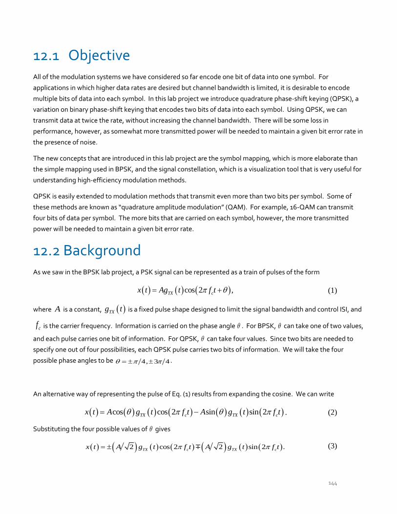
144
12.1 Objective All of the modulation systems we have considered so far encode one bit of data into one symbol. For
applications in which higher data rates are desired but channel bandwidth is limited, it is desirable to encode
multiple bits of data into each symbol. In this lab project we introduce quadrature phase-shift keying (QPSK), a
variation on binary phase-shift keying that encodes two bits of data into each symbol. Using QPSK, we can
transmit data at twice the rate, without increasing the channel bandwidth. There will be some loss in
performance, however, as somewhat more transmitted power will be needed to maintain a given bit error rate in
the presence of noise.
The new concepts that are introduced in this lab project are the symbol mapping, which is more elaborate than
the simple mapping used in BPSK, and the signal constellation, which is a visualization tool that is very useful for
understanding high-efficiency modulation methods.
QPSK is easily extended to modulation methods that transmit even more than two bits per symbol. Some of
these methods are known as “quadrature amplitude modulation” (QAM). For example, 16-QAM can transmit
four bits of data per symbol. The more bits that are carried on each symbol, however, the more transmitted
power will be needed to maintain a given bit error rate.
12.2 Background As we saw in the BPSK lab project, a PSK signal can be represented as a train of pulses of the form
cos 2 ,TX cx t Ag t f t (1)
where A is a constant, TXg t is a fixed pulse shape designed to limit the signal bandwidth and control ISI, and
cf is the carrier frequency. Information is carried on the phase angle . For BPSK, can take one of two values,
and each pulse carries one bit of information. For QPSK, can take four values. Since two bits are needed to
specify one out of four possibilities, each QPSK pulse carries two bits of information. We will take the four
possible phase angles to be 4, 3 4 .
An alternative way of representing the pulse of Eq. (1) results from expanding the cosine. We can write
cos cos 2 sin sin 2TX c TX cx t A g t f t A g t f t . (2)
Substituting the four possible values of gives
2 cos 2 2 sin 2 .TX c TX cx t A g t f t A g t f t (3)

145
We can interpret Eq. (3) to imply that one data bit determines the polarity of the 2 cos 2TX cA g t f t
term (the in-phase term), while the second data bit determines the polarity of the 2 sin 2TX cA g t f t
term (the quadrature term).
To create the transmitted pulse represented by Eq. (1) or (3), we must provide the USRP with the complex
baseband pulse
, 3 4, 4, 4,3 4.j
TXx t Ag t e (4)
In this case the symbol is the complex number jAe . The USRP will generate the transmitted signal of Eq. (1):
2Re cos 2 .cj f t
TX cx t x t e Ag t f t (5)
A convenient way of visualizing the complex signal represented by Eq. (4) is to plot the possible symbol values jAe in the complex plane. A signal constellation for QPSK is shown in Figure 1.
Figure 1. QPSK Signal Constellation
It is easy to see from the signal constellation that there are four possible transmitted signals (hence two bits per
symbol), that each of the possible symbols has the same amplitude A , and that the four possible phase angles
are 4, 3 4 .
146
Let us now examine the relation between pairs of input bits and points in the signal constellation (i.e., symbol
values). The mapping of bit pairs to points in the signal constellation is in fact arbitrary, as long as the
transmitter and receiver use the same mapping. If we associate one bit with the polarity of the real part (in-
phase term) and one bit with the polarity of the imaginary part (quadrature term) we obtain the mapping shown
in Figure 2. As shown in the figure, the right-hand bit governs the polarity of the real part, while the left-hand bit
governs the polarity of the imaginary part. It will be convenient later on to interpret the bit pairs as binary
numbers. In doing this, we will interpret the left-hand bit as the least significant bit, and the right-hand bit as the
most significant bit. This interpretation may seem contrary to intuition, but these bit sequences will be stored as
arrays, and it is natural to write arrays with the index increasing to the right. The symbol mapping can also be
shown in a table. Table 1 is the symbol mapping of Figure 2.
Figure 2. A Possible Symbol Mapping
Table 1. Symbol Mapping
Index Number Bit Pattern Symbol Value
0 00 3 4 2 2jAe A j A
1 10 3 4 2 2jAe A j A
2 01 4 2 2jAe A j A
3 11 4 2 2jAe A j A
147
A QPSK receiver begins with a DSB-SC demodulator. When the transmitted QPSK signal arrives at the receiver
it has the form of a train of pulses, each given by
cos 2 ,TX cr t Dg t f t (6)
where D is a constant (usually much smaller than the constant A in the transmitted signal), the angle carries
the information, and the angle represents the difference in phase between the transmitter and receiver carrier
oscillators. If the receiver’s carrier oscillator is set to the same frequency as the transmitter’s carrier oscillator,
the USRP receiver will do most of the work in demodulating the QPSK signal. The receiver’s Fetch Rx Data will
provide a train of output pulses, each given by10
.
2
j
TX
Dr t g t e
(7)
The pulse train represented by Eq. (7) is passed through a matched filter having impulse response RXg t . If we
write TX RXg t g t g t , then the matched filter output can be written
.
2
jDy t g t e
(8)
The matched filter output is then sampled, at the rate of one sample per symbol. Ideally 0 1g , so the
sampler output is a train of complex numbers of the form
,
2kjD
y k e
(9)
where k is the phase value at the sample time t kT and D and are constants. In practice, the samples
y k will be corrupted by ISI and noise. As in the previous lab project, ISI is removed by an equalizer filter. As
we have seen, the equalizer will also remove the phase error , leaving us with
residual ISI noise.2
kjDy k e
(10)
The remaining receiver steps are detection and symbol mapping. Signal detection is the process of examining
each sample y k and determining for that sample, which symbol is most likely to have been transmitted. It
10 All of the baseband signals are actually represented in LabVIEW as discrete-time signals. Writing them as continuous-time
signals makes the description given here much easier to read.

148
turns out that the algorithm for detection, called a decision rule, is surprisingly simple and has a nice geometric
formulation. Figure 3 shows the signal constellation with the sample y k also shown. Owing to residual ISI
and noise, y k does not correspond exactly to any of the possible symbol values.
Figure 3. Signal Constellation and Received Sample
The decision rule for determining which symbol is most likely to have been transmitted given y k is this:
Calculate the distance between y k and each possible symbol. The most likely symbol is the one at the
smallest distance from y k . In Figure 3, the most likely symbol is the one in the first quadrant. Once the
symbol has been determined, the symbol mapping of Table 1 can be used to convert the symbol to a bit
sequence. For the example of Figure 3, the corresponding bit pattern is 11.
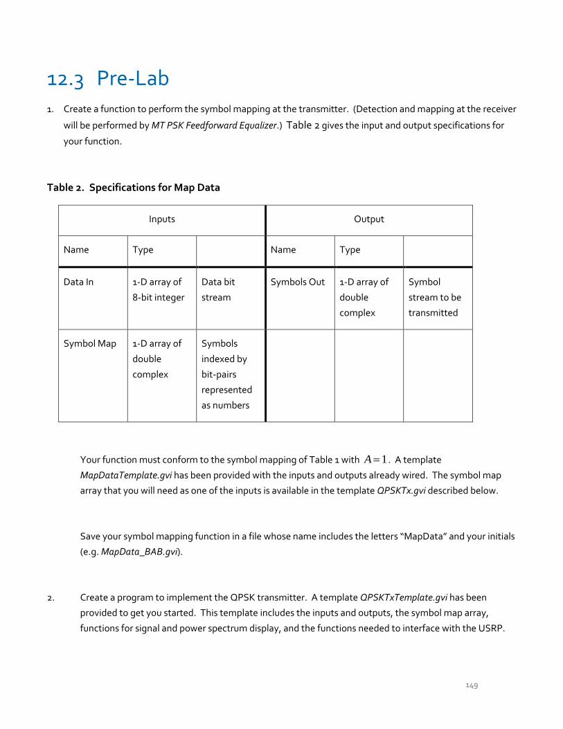
149
12.3 Pre-Lab 1. Create a function to perform the symbol mapping at the transmitter. (Detection and mapping at the receiver
will be performed by MT PSK Feedforward Equalizer.) Table 2 gives the input and output specifications for
your function.
Table 2. Specifications for Map Data
Inputs Output
Name Type Name Type
Data In 1-D array of
8-bit integer
Data bit
stream
Symbols Out 1-D array of
double
complex
Symbol
stream to be
transmitted
Symbol Map 1-D array of
double
complex
Symbols
indexed by
bit-pairs
represented
as numbers
Your function must conform to the symbol mapping of Table 1 with 1A . A template
MapDataTemplate.gvi has been provided with the inputs and outputs already wired. The symbol map
array that you will need as one of the inputs is available in the template QPSKTx.gvi described below.
Save your symbol mapping function in a file whose name includes the letters “MapData” and your initials
(e.g. MapData_BAB.gvi).
2. Create a program to implement the QPSK transmitter. A template QPSKTxTemplate.gvi has been
provided to get you started. This template includes the inputs and outputs, the symbol map array,
functions for signal and power spectrum display, and the functions needed to interface with the USRP.
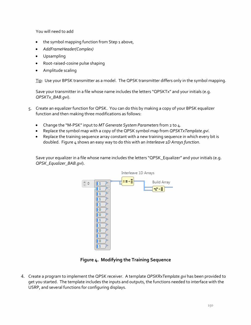
150
You will need to add
the symbol mapping function from Step 1 above,
AddFrameHeader(Complex)
Upsampling
Root-raised-cosine pulse shaping
Amplitude scaling
Tip: Use your BPSK transmitter as a model. The QPSK transmitter differs only in the symbol mapping. Save your transmitter in a file whose name includes the letters “QPSKTx” and your initials (e.g. QPSKTx_BAB.gvi).
5. Create an equalizer function for QPSK. You can do this by making a copy of your BPSK equalizer
function and then making three modifications as follows:
Change the “M-PSK” input to MT Generate System Parameters from 2 to 4.
Replace the symbol map with a copy of the QPSK symbol map from QPSKTxTemplate.gvi.
Replace the training sequence array constant with a new training sequence in which every bit is doubled. Figure 4 shows an easy way to do this with an Interleave 1D Arrays function.
Save your equalizer in a file whose name includes the letters “QPSK_Equalizer” and your initials (e.g. QPSK_Equalizer_BAB.gvi).
Figure 4. Modifying the Training Sequence
4. Create a program to implement the QPSK receiver. A template QPSKRxTemplate.gvi has been provided to get you started. The template includes the inputs and outputs, the functions needed to interface with the USRP, and several functions for configuring displays.

151
Tip: Use your BPSK receiver as a model. The QPSK receiver is very similar. You will need to add
Channel.gvi.
Use a Cluster Properties function after the Channel.gvi to give access to its “Y” component, an array of double complex sample values.
Root-raised-cosine matched filter and the Convolution function to implement the filter. Note: There is no phase synchronizer, since this function will be performed by the equalizer. Also, do not take the real part of the received sample values.
Using a Cluster Properties function, create a complex double cluster from the output of Convolution.
PulseAlign (Complex).
Use a Cluster Properties function after the PulseAlign(Complex) to give access to the “Y” component. Add Decimate (single shot) to sample the aligned pulses.
FrameSync(Complex).
Your equalizer from Step 3 above comes next. The “Output Signal” from FrameSync(Complex) is the equalizer input. Do not use the “Aligned Samples” FrameSync(Complex) output.
Connect the “Output Bits” equalizer output to an Array Subset function. Set the “index” to 52 to remove the training sequence header and set the “length” to the number of message bits. The output of Array Subset function can be displayed as the receiver’s “Output Bits” and can also be sent to MT Calculate BER.
There are two MT Format Eye Diagram functions in the template. Connect the first one to the “Output Signal” from PulseAlign(Complex). This will display the eye diagram of the in-phase component of the received signal before equalization. Connect the second eye diagram to “Output Complex Waveform” from the equalizer. This will display the eye diagram of the in-phase component of the received signal after equalization.
Also connect the “Output Complex Waveform” from the equalizer to the “waveform” input of MT Format Constellation. Save your receiver in a file whose name includes the letters “QPSKRx” and your initials (e.g. QPSKRx_BAB.gvi).
Questions
1. The symbol rate of your transmitter and receiver is 10,000 symbols/second. What is the data rate in bits/second?
2. If the receiver is set for an IQ rate of 200 kHz, how many samples per symbol will there be at the receiver? 3. The spectral efficiency of a modulated signal is the data rate in bits/second divided by the bandwidth of the
transmitted signal. Calculate the spectral efficiency of the BPSK signal using root-raised-cosine pulses that you generated in the BPSK lab project. Compare with the spectral efficiency of a QPSK signal, assuming that the bandwidth remains the same.

152
12.4 Lab Procedure 1. Connect a loopback cable and attenuator between the TX 1 and RX 2 connectors of the USRP. Connect
the USRP to your computer and plug in the power to the USRP. Run LabVIEW and open the transmitter
that you created in the prelab.
2. Ensure that the transmitter is set up to use
Carrier Frequency: 915.0 MHz
IQ Rate: 200 kHz. Note: This sets the value of 1 xT .
Gain: 0 dB
Active Antenna: TX1
Symbol rate: 10,000 symbols/s
Message Length: 1000 bits
Pulse shaping filter: Root Raised
3. Run the transmitter. Use the large STOP button on the front panel to stop transmission connectors.
4. Using the power spectrum display on the transmitter front panel, measure the bandwidth of the complex
baseband signal.
5. Ensure that the receiver is set up to use
Carrier Frequency: 915.0 MHz
IQ Rate: 200 kHz. Note: This sets the value of 1 zT . Note that zT is the same parameter as dt .
Gain: 0 dB
Active Antenna: RX2
Symbol rate: 10,000 symbols/s
Message Length: 1000 bits
Pulse shaping filter: Root Raised
Use Channel: off

153
6. Run the transmitter, then run the receiver. Once the receiver has acquired its data, you may stop the
transmitter. The receiver should show a BER of 0.0.
7. Compare the eye diagram before and after equalization. Run the receiver a dozen times or so until you get a
feel for what changes from run to run and what does not. Occasionally the “before” eye diagram will show
four sample values rather than two. Take screenshots of the “before” and “after” eye diagrams for this case.
8. Set Use Channel to “on,” with the default channel model, and a propagation delay of 100 s . Run the
transmitter and then run the receiver several times. Compare the eye diagrams before and after
equalization. Measure the eye opening before and after equalization. Try to get a worst-case “before”
scenario for your measurement.
9. Set Use Channel to “off,” and run the transmitter and receiver again. This time observe the signal
constellation. Take a screenshot of the constellation.
10. Change the wiring to MT Format Constellation so that the input is taken from the FrameSync(Complex)
“Output Signal” instead of from the equalizer. Run the transmitter and then run the receiver several times.
What happens to the angle of the signal constellation? What happens to the radius of the signal
constellation?
Questions
1. What is the measured bandwidth of the transmitted QPSK signal? (Note: Not the baseband signal
bandwidth.) Compare with the bandwidth of the BPSK signal that you measured in an earlier lab project.
2. Report your eye opening measurement results from Step 6.
3. What is the cause of the signal constellation rotation that you observed in Step 8? What does the signal
constellation look like when the “before” eye diagram shows four sample values rather than two?

154
Explain why the eye diagram appears as it does. Hint: Remember that the eye diagram plot displays
only the in-phase component of the signal.
4. What would the signal constellation look like if the transmitter and receiver carrier frequencies were
slightly different?
6. What would you expect to be the effect of rotation of the signal constellation on the BER? (Assume that
the equalizer is not present.)
7. Observe the transition traces on the signal constellation graph. Notice that transitions between first and
third quadrant signals pass through the origin of the graph, as do transitions between second and fourth
quadrant signals. Describe what is happening to the amplitude of the received signal when these
transitions occur.
12.5 Report
Prelab
Hand in documentation for the four functions you created: the symbol mapping, the transmitter, the equalizer,
and the receiver. Also include documentation for any functions you may have created. To obtain
documentation, print out legible screenshots of the front panel and block diagram.
Answer all of the questions in the Prelab section marked Questions.
Lab
Submit the symbol mapping, transmitter, equalizer, and receiver programs. Resubmit documentation for any
functions you modified during the lab.
Submit the plots asked for in Steps 5 and 7.
Answer the questions in the Lab Procedure section marked Questions.