Embed Size (px)
Citation preview
Fujitsu Microelectronics Europe Application Note
MCU-AN-300072-E-V13
FR FAMILY 32-BIT MICROCONTROLLER
MB91460
I2C
APPLICATION NOTE
I2C Revision History
MCU-AN-300072-E-V13 - 2 - © Fujitsu Microelectronics Europe GmbH
Revision History
Date Issue 2008-02-26 V1.0, First draft, HPi 2008-03-19 V1.1 Updated Example and Description, HPi 2008-05-30 V1.2 Updated chapter 3, HPi 2008-06-11 V1.3 Reworked on source code, HPi
This document contains 30 pages.

I2C Warranty and Disclaimer
© Fujitsu Microelectronics Europe GmbH - 3 - MCU-AN-300072-E-V13
Warranty and Disclaimer To the maximum extent permitted by applicable law, Fujitsu Microelectronics Europe GmbH restricts its warranties and its liability for all products delivered free of charge (eg. software include or header files, application examples, target boards, evaluation boards, engineering samples of IC’s etc.), its performance and any consequential damages, on the use of the Product in accordance with (i) the terms of the License Agreement and the Sale and Purchase Agreement under which agreements the Product has been delivered, (ii) the technical descriptions and (iii) all accompanying written materials. In addition, to the maximum extent permitted by applicable law, Fujitsu Microelectronics Europe GmbH disclaims all warranties and liabilities for the performance of the Product and any consequential damages in cases of unauthorised decompiling and/or reverse engineering and/or disassembling. Note, all these products are intended and must only be used in an evaluation laboratory environment.
1. Fujitsu Microelectronics Europe GmbH warrants that the Product will perform substantially in accordance with the accompanying written materials for a period of 90 days form the date of receipt by the customer. Concerning the hardware components of the Product, Fujitsu Microelectronics Europe GmbH warrants that the Product will be free from defects in material and workmanship under use and service as specified in the accompanying written materials for a duration of 1 year from the date of receipt by the customer.
2. Should a Product turn out to be defect, Fujitsu Microelectronics Europe GmbH´s entire liability and the customer´s exclusive remedy shall be, at Fujitsu Microelectronics Europe GmbH´s sole discretion, either return of the purchase price and the license fee, or replacement of the Product or parts thereof, if the Product is returned to Fujitsu Microelectronics Europe GmbH in original packing and without further defects resulting from the customer´s use or the transport. However, this warranty is excluded if the defect has resulted from an accident not attributable to Fujitsu Microelectronics Europe GmbH, or abuse or misapplication attributable to the customer or any other third party not relating to Fujitsu Microelectronics Europe GmbH.
3. To the maximum extent permitted by applicable law Fujitsu Microelectronics Europe GmbH disclaims all other warranties, whether expressed or implied, in particular, but not limited to, warranties of merchantability and fitness for a particular purpose for which the Product is not designated.
4. To the maximum extent permitted by applicable law, Fujitsu Microelectronics Europe GmbH´s and its suppliers´ liability is restricted to intention and gross negligence.
NO LIABILITY FOR CONSEQUENTIAL DAMAGES
To the maximum extent permitted by applicable law, in no event shall Fujitsu Microelectronics Europe GmbH and its suppliers be liable for any damages whatsoever (including but without limitation, consequential and/or indirect damages for personal injury, assets of substantial value, loss of profits, interruption of business operation, loss of information, or any other monetary or pecuniary loss) arising from the use of the Product.
Should one of the above stipulations be or become invalid and/or unenforceable, the remaining stipulations shall stay in full effect
I2C Contents
MCU-AN-300072-E-V13 - 4 - © Fujitsu Microelectronics Europe GmbH
Contents
REVISION HISTORY............................................................................................................ 2
WARRANTY AND DISCLAIMER ......................................................................................... 3
CONTENTS .......................................................................................................................... 4
1 INTRODUCTION.............................................................................................................. 6
2 REGISTERS..................................................................................................................... 7 2.1 Bus Control Register (IBCR0) ................................................................................. 7
2.2 Bus Status Register (IBSR0)................................................................................... 8 2.3 Ten Bit Slave Address Register (ITBA0)................................................................. 8
2.4 Ten Bit Address Mask Register (ITMK0) ................................................................. 8 2.5 Seven Bit Slave Address Register (ISBA0) ............................................................. 9
2.6 Seven Bit Address Mask Register (ISMK0) ............................................................. 9 2.7 Data Register (IDAR0) ............................................................................................ 9
2.8 Clock Control Register (ICCR0)............................................................................... 9
3 I2C OPERATION ........................................................................................................... 10 3.1 Start Condition ...................................................................................................... 10 3.2 Stop Condition....................................................................................................... 10 3.3 Slave Address Detection ....................................................................................... 10 3.4 Slave Address Masking......................................................................................... 10 3.5 Addressing Slaves................................................................................................. 11 3.6 Acknowledgement ................................................................................................. 11
4 INTERFACING TO EEPROM......................................................................................... 12 4.1 EEPROM............................................................................................................... 12 4.2 Connection to MB914xx ........................................................................................ 12 4.3 Addressing ............................................................................................................ 13 4.4 Example Code....................................................................................................... 13
4.4.1 Initial Functions and Declarations........................................................ 13 4.4.1.1 Flowchart ................................................................................. 13 4.4.1.2 C Code .................................................................................... 14
4.4.2 Write EEPROM ....................................................................................... 14 4.4.2.1 Timing Diagram ....................................................................... 14 4.4.2.2 Flowchart ................................................................................. 15 4.4.2.3 Code........................................................................................ 16
4.4.3 Read from EEPROM .............................................................................. 17
I2C Contents
© Fujitsu Microelectronics Europe GmbH - 5 - MCU-AN-300072-E-V13
4.4.3.1 Timing Diagram ....................................................................... 17 4.4.3.2 Flowchart ................................................................................. 18 4.4.3.3 Code........................................................................................ 19
4.4.4 Master mode using Interrupt................................................................. 20 4.4.4.1 Timing Diagram ....................................................................... 20 4.4.4.2 Flowchart ................................................................................. 21 4.4.4.3 Code........................................................................................ 22
5 SLAVE MODE USING INTERRUPT .............................................................................. 25 5.1.1.1 Timing Diagram ....................................................................... 25 5.1.1.2 Flowchart ................................................................................. 26 5.1.1.3 Code........................................................................................ 27
6 APPENDIX..................................................................................................................... 29 6.1 List of Figures........................................................................................................ 29 6.2 List of Tables......................................................................................................... 29
7 ADDITIONAL INFORMATION ....................................................................................... 30
I2C Chapter 1 Introduction
MCU-AN-300072-E-V13 - 6 - © Fujitsu Microelectronics Europe GmbH
1 Introduction I2C is a two-wire serial bus. There is no need for chip select or arbitration logic, making it cheap and simple to implement in hardware. The two I2C signals are serial data (SDA) and serial clock (SCL) and are both bi-directional. These are open drain output hence one need to connect pull up register on the SDA and SCL line.
The device that initiates a transaction on the I2C bus is termed the master. The master normally controls the clock signal. A device being addressed by the master is called a slave.
Each I2C-compatible hardware slave device comes with a predefined device address, the lower bits of which may be configurable at the board level. The master transmits the device address of the intended slave at the beginning of every transaction. Each slave is responsible for monitoring the bus and responding only to its own address.
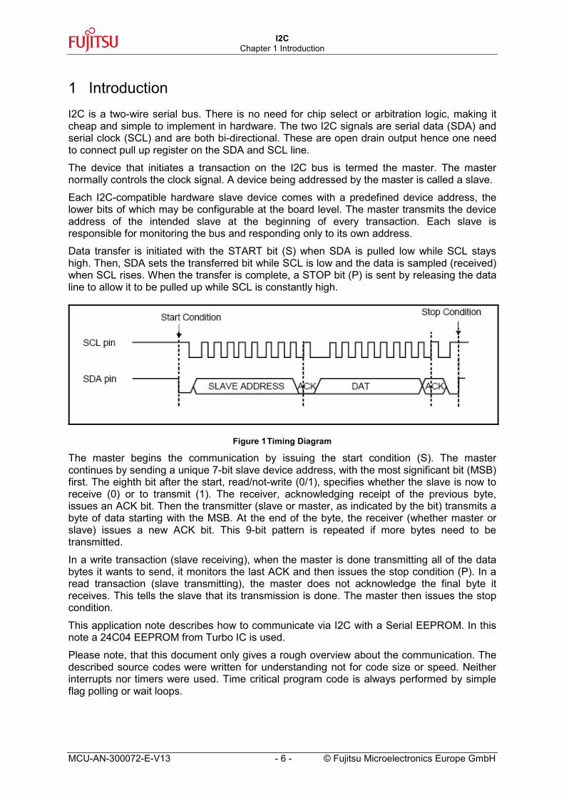
Data transfer is initiated with the START bit (S) when SDA is pulled low while SCL stays high. Then, SDA sets the transferred bit while SCL is low and the data is sampled (received) when SCL rises. When the transfer is complete, a STOP bit (P) is sent by releasing the data line to allow it to be pulled up while SCL is constantly high.
Figure 1 Timing Diagram
The master begins the communication by issuing the start condition (S). The master continues by sending a unique 7-bit slave device address, with the most significant bit (MSB) first. The eighth bit after the start, read/not-write (0/1), specifies whether the slave is now to receive (0) or to transmit (1). The receiver, acknowledging receipt of the previous byte, issues an ACK bit. Then the transmitter (slave or master, as indicated by the bit) transmits a byte of data starting with the MSB. At the end of the byte, the receiver (whether master or slave) issues a new ACK bit. This 9-bit pattern is repeated if more bytes need to be transmitted.
In a write transaction (slave receiving), when the master is done transmitting all of the data bytes it wants to send, it monitors the last ACK and then issues the stop condition (P). In a read transaction (slave transmitting), the master does not acknowledge the final byte it receives. This tells the slave that its transmission is done. The master then issues the stop condition.
This application note describes how to communicate via I2C with a Serial EEPROM. In this note a 24C04 EEPROM from Turbo IC is used.
Please note, that this document only gives a rough overview about the communication. The described source codes were written for understanding not for code size or speed. Neither interrupts nor timers were used. Time critical program code is always performed by simple flag polling or wait loops.
I2C Chapter 2 Registers
© Fujitsu Microelectronics Europe GmbH - 7 - MCU-AN-300072-E-V13
2 Registers
2.1 Bus Control Register (IBCR0)The IBCR0 consists of the following bits:
Bit No.
Bit Name
Initial Value Value Description
0 Clear bus error interrupt flag* 1 No effect*
0 No bus error detected+15 BER 0
1 One of the error conditions described below detected+
0 Bus error interrupt request disabled 14 BEIE 0 1 Bus error interrupt request enabled
0 No effect 13 SCC 0 1 Generate repeated start condition during master transfer
0 Go to slave mode 12 MSS 0 1 Go to master mode, generate start condition and send address
data byte in IDAR0 register
0 The interface will not acknowledge on data byte reception 11 ACK 0 1 The interface will acknowledge on data byte reception
0 The interface will not acknowledge on general call address byte reception
10 GCAA 01 The interface will acknowledge on general call address byte
reception 0 Interrupt request disabled
9 INTE 0 1 Interrupt request enabled
0 Clear transfer end interrupt flag*
1 No effect*
0 Transfer not ended or not involved in current transfer or bus is idle+
8 INT 0
1
Set at the end of a 1-byte data transfer or reception including the acknowledge bit under the following conditions: • Device is bus master. • Device is addressed as slave. • General call address received. • Arbitration loss occurred. Set at the end of an address data reception (after first byte if seven bit address received, after second byte if ten bit address received) including the acknowledge bit if the device is addressed as slave. +
+ Read Access * Write Access
I2C Chapter 2 Registers
MCU-AN-300072-E-V13 - 8 - © Fujitsu Microelectronics Europe GmbH
2.2 Bus Status Register (IBSR0)The IBCR0 consists of the following bits:
Bit No.
Bit Name
Initial Value Value Description
0 Stop condition detected (bus idle) 7 BB 0 1 Start condition detected (bus in use)
0 Repeated start condition not detected 6 RCS 0 1 Bus in use, repeated start condition detected
0 No arbitration loss detected 5 AL 0 1 Arbitration loss occurred during master sending
0 Receiver acknowledged 4 LRB 0 1 Receiver did not acknowledge
0 Not transmitting data 3 TRX 0 1 Transmitting data
0 Not addressed as slave 2 AAS 0 1 Addressed as slave
0 General call address not received as slave 1 GCA 0 1 General call address received as slave
0 Incoming data is not address data (or bus is not in use) 0 ADT 0 1 Incoming data is address data
2.3 Ten Bit Slave Address Register (ITBA0)This register (ITBAH0 / ITBAL0) designates the ten bit slave address.
Bit No.
Bit Name
Initial Value Value Description
15-10 RES 09-0 TAn 1 Address bits
2.4 Ten Bit Address Mask Register (ITMK0)This register contains the ten bit slave address mask and the ten bit slave address enable bit
Bit No.
Bit Name
Initial Value Value Description
0 Ten bit slave address disabled 15 ENTB 0 1 Ten bit slave address enabled
0 Addressed as seven bit slave. 14 RAL 0 1 Addressed as ten bit slave
13-10 RES 10 Bit is not used in slave address comparison
9-0 TMn 1 1 Bit is used in slave address comparison.
I2C Chapter 2 Registers
© Fujitsu Microelectronics Europe GmbH - 9 - MCU-AN-300072-E-V13
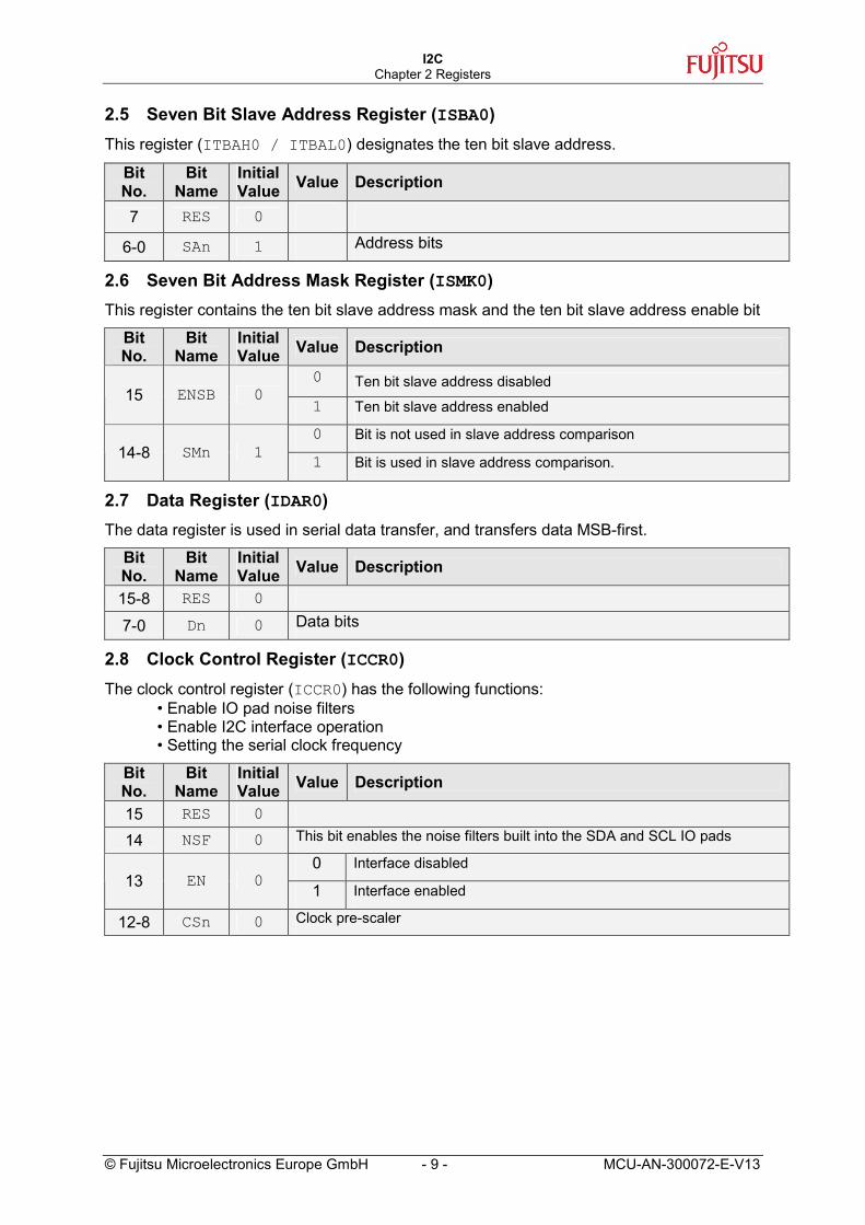
2.5 Seven Bit Slave Address Register (ISBA0)This register (ITBAH0 / ITBAL0) designates the ten bit slave address.
Bit No.
Bit Name
Initial Value Value Description
7 RES 06-0 SAn 1 Address bits
2.6 Seven Bit Address Mask Register (ISMK0)This register contains the ten bit slave address mask and the ten bit slave address enable bit
Bit No.
Bit Name
Initial Value Value Description
0 Ten bit slave address disabled 15 ENSB 0 1 Ten bit slave address enabled
0 Bit is not used in slave address comparison 14-8 SMn 1 1 Bit is used in slave address comparison.
2.7 Data Register (IDAR0)The data register is used in serial data transfer, and transfers data MSB-first.
Bit No.
Bit Name
Initial Value Value Description
15-8 RES 07-0 Dn 0 Data bits
2.8 Clock Control Register (ICCR0)The clock control register (ICCR0) has the following functions:
• Enable IO pad noise filters • Enable I2C interface operation • Setting the serial clock frequency
Bit No.
Bit Name
Initial Value Value Description
15 RES 014 NSF 0 This bit enables the noise filters built into the SDA and SCL IO pads
0 Interface disabled 13 EN 0
1 Interface enabled
12-8 CSn 0 Clock pre-scaler
I2C Chapter 3 I2C Operation
MCU-AN-300072-E-V13 - 10 - © Fujitsu Microelectronics Europe GmbH
3 I2C Operation
THIS CHAPTER DESCRIBES OPERATION OF I2C
3.1 Start Condition When the bus is free (IBSRn: BB = 0, IBCRn: MSS = 0), writing ‘1’ to the IBCRn: MSS bit places the I2C interface in master mode and generates a start condition and the contents of the IDAR0 register (which should be address data) is sent.
Repeated start conditions can be generated by writing ‘1’ to the IBCRn: SCC bit when in bus master mode and interrupt status (IBCRn: MSS=1 and IBCRn: INT=1).
If a 1 is written to the IBCR0: MSS bit while the bus is in use (IBSRn: BB=1 and IBSRn: TRX=0; IBCRn: MSS=0 and IBCRn: INT=0), the interface waits until the bus is free and then starts sending.
Writing ‘1’ to the MSS bit or SCC bit in any other situation has no significance.
3.2 Stop Condition Writing ‘0’ to the IBCRn: MSS bit in master mode (IBCRn: MSS=1 and IBCRn: INT=1)generates a stop condition and places the device in slave mode. Writing ‘0’ to the IBCRn: MSS bit in any other situation has no significance.
After clearing the IBCRn: MSS bit, the interface tries to generate a stop condition which might fail if another master pulls the SCL line low before the stop condition has been generated. This will generate an interrupt after the next byte has been transferred.
3.3 Slave Address Detection In slave mode, after a start condition is generated the IBSRn: BB is set to ‘1’ and data sent from the master device is received into the IDARn register. After the reception of eight bits, the contents of the IDARn register is compared to the ISBAn register using the bit mask stored in ISMKn if the ISMKn: ENSB bit is ‘1’.
If a match results, the IBSRn: AAS bit is set to ‘1’ and an acknowledge signal is sent to the master. Then bit 0 of the received data (bit 0 of the IDARn register) is inverted and stored in the IBSRn: TRX bit.
If the ITMKn: ENTB bit is ‘1’ and a ten bit address header is detected, the interface sends an acknowledge signal to the master and stores the inverted last data bit in the IBSRn: TRX register. No interrupt is generated. Then, the next transferred byte is compared (using the bit mask stored in ITMKn) to the lower byte of the ITBAn register. If a match is found, an acknowledge signal is sent to the master, the IBSRn: AAS bit is set and an interrupt is generated.
3.4 Slave Address Masking Only the bits set to ‘1’ in the mask registers (ITMKn / ISMKn) are used for address comparison, all other bits are ignored. The received slave address can be read from the ITBAn (if ten bit address received, ITMKn: RAL=1) or ISBAn (if seven bit address received, ISMKn: RAL=‘0’) register if the IBSRn: AAS bit is ‘1’.
If the bitmasks are cleared, the interface can be used as a bus monitor since it will always be addressed as slave. Note that this is not a real bus monitor because it acknowledges upon any slave address reception, even if there is no other slave listening.
I2C Chapter 3 I2C Operation
© Fujitsu Microelectronics Europe GmbH - 11 - MCU-AN-300072-E-V13
3.5 Addressing Slaves In master mode, after a start condition is generated the IBSRn: BB and IBSRn: TRX bits are set to ‘1’ and the contents of the IDARn register is sent in MSB first order. After address data is sent and an acknowledge signal was received from the slave device, bit 0 of the sent data (bit 0 of the IDARn register after sending) is inverted and stored in the IBSRn: TRX bit.
Acknowledgement by the slave may be checked using the IBSRn: LRB bit. This procedure also applies to a repeated start condition.
In order to address a ten bit slave for write access, two bytes have to be sent. The first one is the ten bit address header which consists of the bit sequence ‘1 1 1 1 0 A9 A8 0’, it is followed by the second byte containing the lower eight bits of the ten bit slave address (A7 - A0). A ten bit slave is accessed for reading by sending the above byte sequence and generating a repeated start condition (IBSRn: SCC) followed by a ten bit address header with read access (1 1 1 1 0 A9 A8 1). Summary of the address data bytes: 7 bit slave, write access: Start condition - A6 A5 A4 A3 A2 A1 A0 0 7 bit slave, read access: Start condition - A6 A5 A4 A3 A2 A1 A0 1 10 bit slave, write access: Start condition - 1 1 1 1 0 A9 A8 0 - A7 A6 A5 A4 A3 A2 A1 A0 10 bit slave, read access: Start condition - 1 1 1 1 0 A9 A8 1 - A7 A6 A5 A4 A3 A2 A1 A0 - repeated start - 1 1 1 1 0 A9 A8 1
3.6 Acknowledgement Acknowledge bits are sent from the receiver to the transmitter. The IBCRn: ACK bit can be used to select whether to send an acknowledgment when data bytes are received.
When data is sent in slave mode (read access from another master), if no acknowledgement is received from the master, the IBSRn: TRX bit is set to ‘0’ and the device goes to receiving mode. This enables the master to generate a stop condition as soon as the slave has released the SCL line. In master mode, acknowledgement by the slave may be checked by reading the IBSRn: LRB bit.

I2C Chapter 4 Interfacing to EEPROM
MCU-AN-300072-E-V13 - 12 - © Fujitsu Microelectronics Europe GmbH
4 Interfacing to EEPROM
THIS CHAPTER DESCRIBES HOW TO COMMUNICATE WITH THE 24C04 EEPROM
4.1 EEPROM The 24LC04 serial EEPROM from Turbo IC has 4096-Bit memory size, organized as 512 x 8 Bits.
The 24LC04 has the following pin-out:
•NC 1 8 Vcc
A1 2 7 WP
A2 3 6 SCL
Vss 4 5 SDA
Figure 2 Pin Diagram of EEPROM 24LC04
Pin names:
NC Not connected A1 Address select 1 A2 Address select 2 Vss Ground SDA Serial Data SCL Serial Clock WP Write Protect Vcc Power Supply (+ 5 volts)
Table 1 Pin names of EEPROM 24LC04
4.2 Connection to MB914xx The EEPROM can be connected as in the following schematic. Please note, that no power supply pins and other MCU-Pins are drawn than those for the connection to the EEPROM.
Figure 3 Connection block diagram
MB914xx 24C04
SDA
SCL
I2C Chapter 4 Interfacing to EEPROM
© Fujitsu Micr
4.3 Addressing The EEPROM uses the 8-bit addressing scheme of the I2C bus. The 4 most significant bits are fixed to “1010”. The A1 and A2 lines of the chip select the next two address bits. The next bit is the least significant bit of the memory address. The last address bit select Read or Write operation, as defined by the I2C standard.
The actual aonly be set access for th
4.4 ExamThe followinthe MB91F4
4.4.1 Initia
4.4.1.1 Flo
D
Set (ICC
Clea
Dis
1
oelectro
ddressby a wrat addr
ple Cog code 67D.
l Func
wchart
isable
clock R0: CS
r data r
able Bu
Enable
Clear B
0
nics Eur
that is ite operess is r
de shows h
tions
I2C Int
I2C bits)
egister
s Error
I2C inte
us Erro
1
ope Gm
written ation, iequired
ow to e
and De
erface
presca
interrup
rface
r flag
0
bH
to or re.e. if a before
stablish
clarat
I2
ler
t
A2
- 13 -
ad fromcertain reading
a com
ions
C_Ini
A1
is tranmemory it.
munica
t
A0
smitted addre
tion to a
Dis
Disabl
Enable
D
Cle
R/W
MCU-AN-300072-E-V13
as the first data byte. It can ss needs to be read, a write
nd from the EEPROM using
able sending of Acknowledge
e generation of Call Acknowledge
inputs for SDA, SCL
isable interrupt
ar interrupt flag
I2C Chapter 4 Interfacing to EEPROM
MCU-AN-300072-E-V13 - 14 - © Fujitsu Microelectronics Europe GmbH
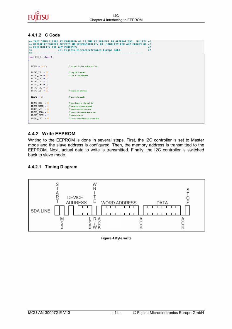
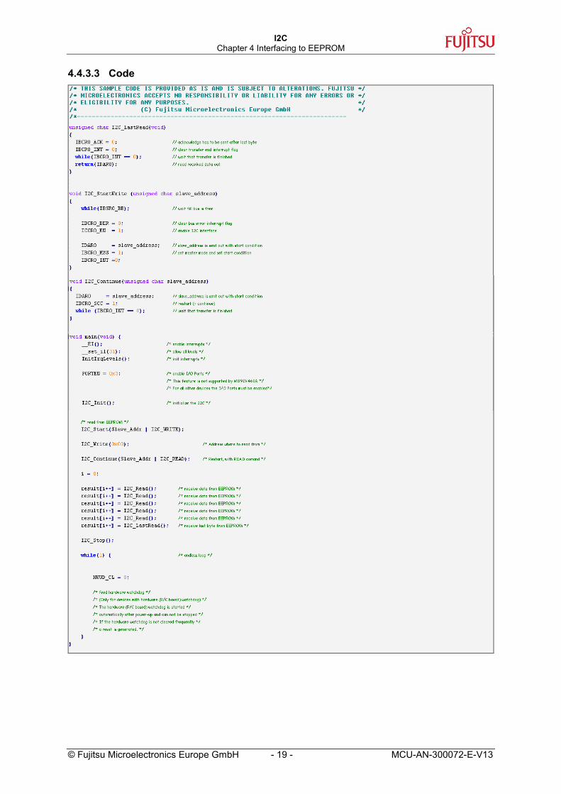
4.4.1.2 C Code
4.4.2 Write EEPROM Writing to the EEPROM is done in several steps. First, the I2C controller is set to Master mode and the slave address is configured. Then, the memory address is transmitted to the EEPROM. Next, actual data to write is transmitted. Finally, the I2C controller is switched back to slave mode.
4.4.2.1 Timing Diagram
Figure 4 Byte write
I2C Chapter 4 Interfacing to EEPROM
© Fujitsu Microelectronics Europe GmbH - 15 - MCU-AN-300072-E-V13
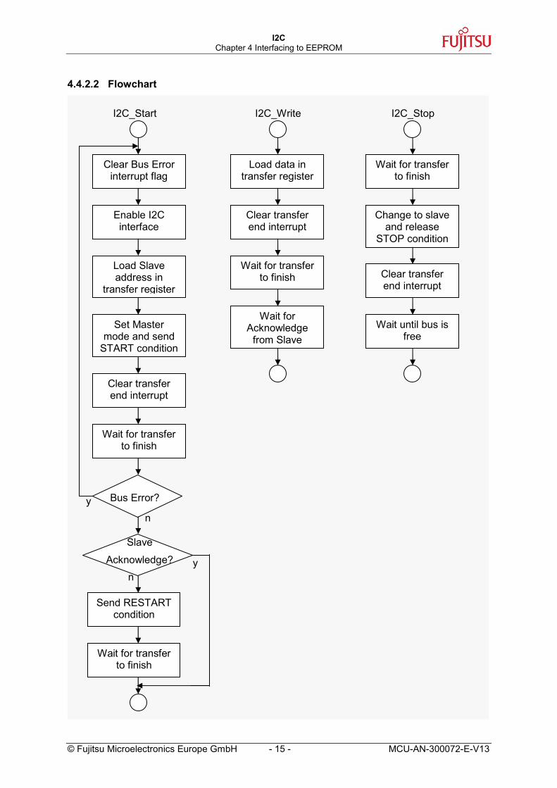
4.4.2.2 Flowchart
Load data in transfer register
Clear transfer end interrupt
Wait for transfer to finish
Wait for Acknowledge
from Slave
Wait for transfer to finish
Change to slave and release
STOP condition
Clear transfer end interrupt
Wait until bus is free
I2C_Start I2C_Write I2C_Stop
Clear Bus Error interrupt flag
Enable I2C interface
Load Slave address in
transfer register
Set Master mode and send
START condition
Clear transfer end interrupt
Bus Error?
Wait for transfer to finish
Slave
Acknowledge?
Send RESTART condition
Wait for transfer to finish
y
y
n
n
I2C Chapter 4 Interfacing to EEPROM
MCU-AN-300072-E-V13 - 16 - © Fujitsu Microelectronics Europe GmbH
4.4.2.3 Code
I2C Chapter 4 Interfacing to EEPROM
© Fujitsu Microelectronics Europe GmbH - 17 - MCU-AN-300072-E-V13
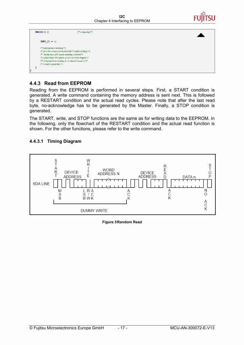
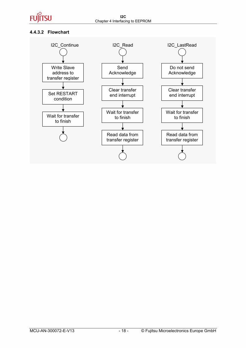
4.4.3 Read from EEPROM Reading from the EEPROM is performed in several steps. First, a START condition is generated. A write command containing the memory address is sent next. This is followed by a RESTART condition and the actual read cycles. Please note that after the last read byte, no-acknowledge has to be generated by the Master. Finally, a STOP condition is generated.
The START, write, and STOP functions are the same as for writing data to the EEPROM. In the following, only the flowchart of the RESTART condition and the actual read function is shown. For the other functions, please refer to the write command.
4.4.3.1 Timing Diagram
Figure 5 Random Read
I2C Chapter 4 Interfacing to EEPROM
MCU-AN-300072-E-V13 - 18 - © Fujitsu Microelectronics Europe GmbH
4.4.3.2 Flowchart
Send Acknowledge
Clear transfer end interrupt
Wait for transfer to finish
Read data from transfer register
Do not send Acknowledge
Clear transfer end interrupt
Wait for transfer to finish
Read data from transfer register
I2C_Read I2C_LastRead I2C_Continue
Write Slave address to
transfer register
Set RESTART condition
Wait for transfer to finish
I2C Chapter 4 Interfacing to EEPROM
© Fujitsu Microelectronics Europe GmbH - 19 - MCU-AN-300072-E-V13
4.4.3.3 Code

I2C Chapter 4 Interfacing to EEPROM
MCU-AN-300072-E-V13 - 20 - © Fujitsu Microelectronics Europe GmbH
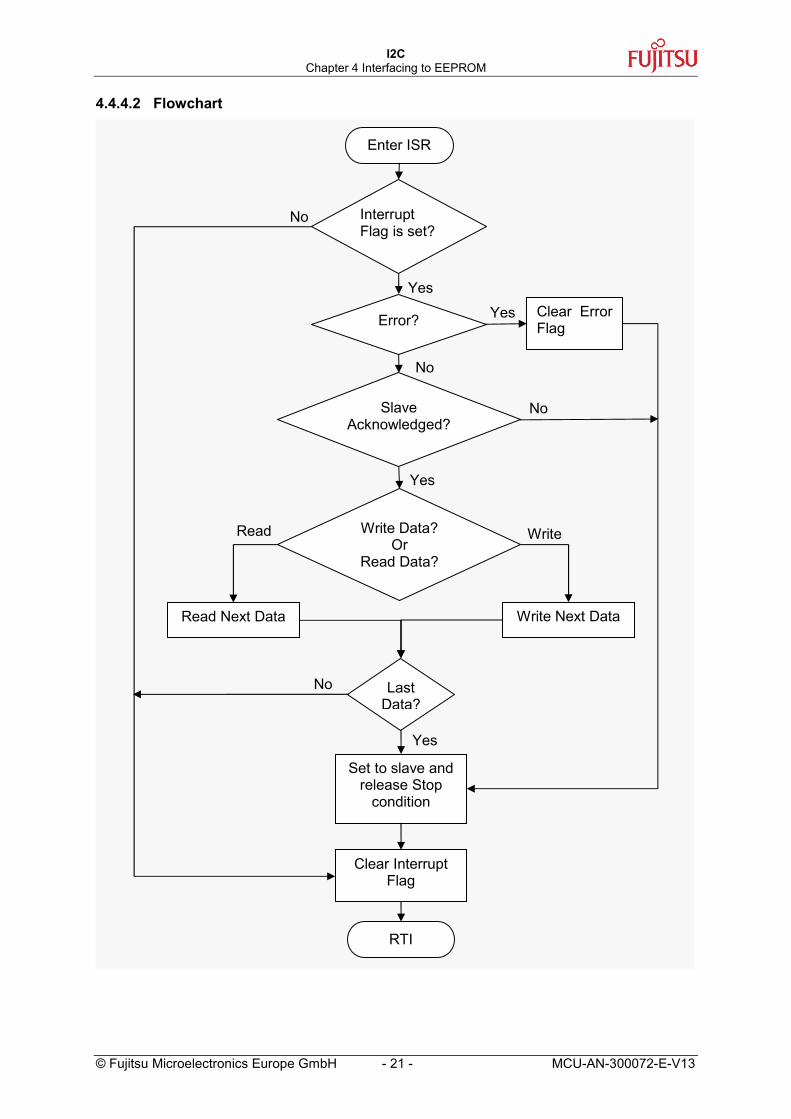
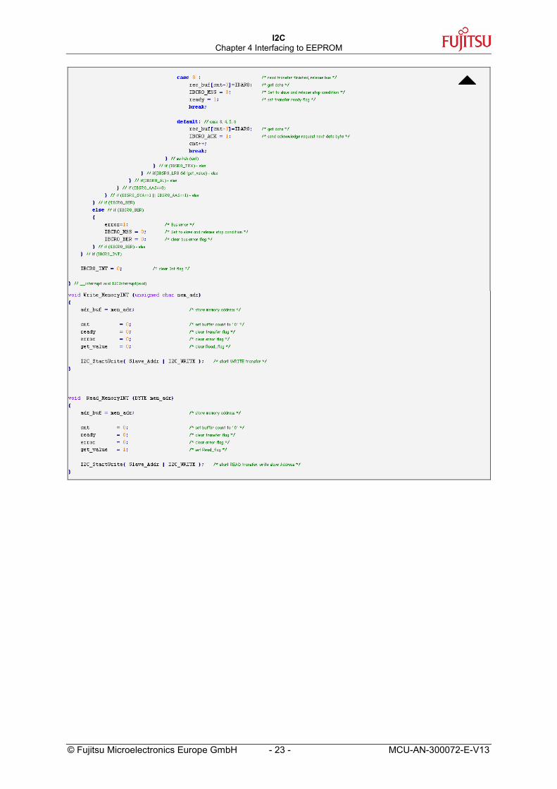
4.4.4 Master mode using Interrupt Here actual read and write of data is carried out in Interrupt service routine.
In master mode, after a start condition is generated the contents of the Data (IDARn)register are sent in MSB first order. After address data is sent and an acknowledge signal was received from the slave device, bit 0 of the sent data (bit 0 of the IDAR0 register after sending) is inverted and stored in the TRX bit. Acknowledgement by the slave may be checked using the LRB bit in the IBSR0 register. This procedure also applies to a repeated start condition.
4.4.4.1 Timing Diagram
Figure 6 Master read/write
Control Byte
Continue SDA Line
SDA Line
Control Byte
S: Start
P: Stop A: Acknowledge NA: No Acknowledge
Continue
S A Address Pointer A Data A P
Bus Activity – Master Write
Master Interrupt
Slave Address W
S A Address Pointer AW S R
Master Interrupt
Data NA P
Master Interrupt
Bus Activity – Master Read
Data sent to slave from Master
Data received to Master from slave
A
Control Byte
Slave Address Slave Address
A6-A0
A6-A0 A6-A0
I2C Chapter 4 Interfacing to EEPROM
© Fujitsu Microelectronics Europe GmbH - 21 - MCU-AN-300072-E-V13
4.4.4.2 Flowchart
Yes
Interrupt Flag is set?
Error?
Slave Acknowledged?
Write Data? Or
Read Data?
Read Next Data Write Next Data
Set to slave and release Stop
condition
Clear Error Flag
Clear Interrupt Flag
RTI
Enter ISR
Yes
No
No
No
Yes
Write Read
Last Data?
Yes
No
I2C Chapter 4 Interfacing to EEPROM
MCU-AN-300072-E-V13 - 22 - © Fujitsu Microelectronics Europe GmbH
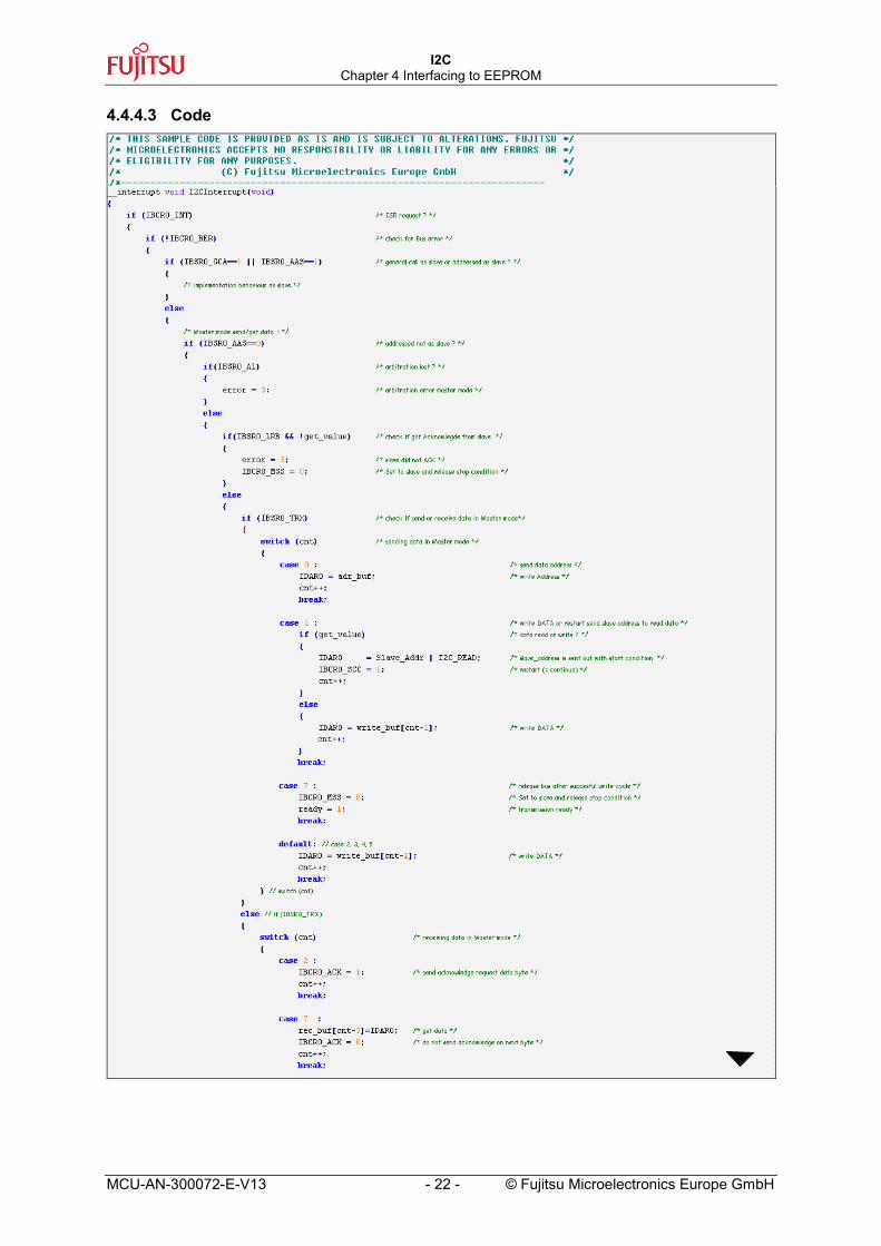
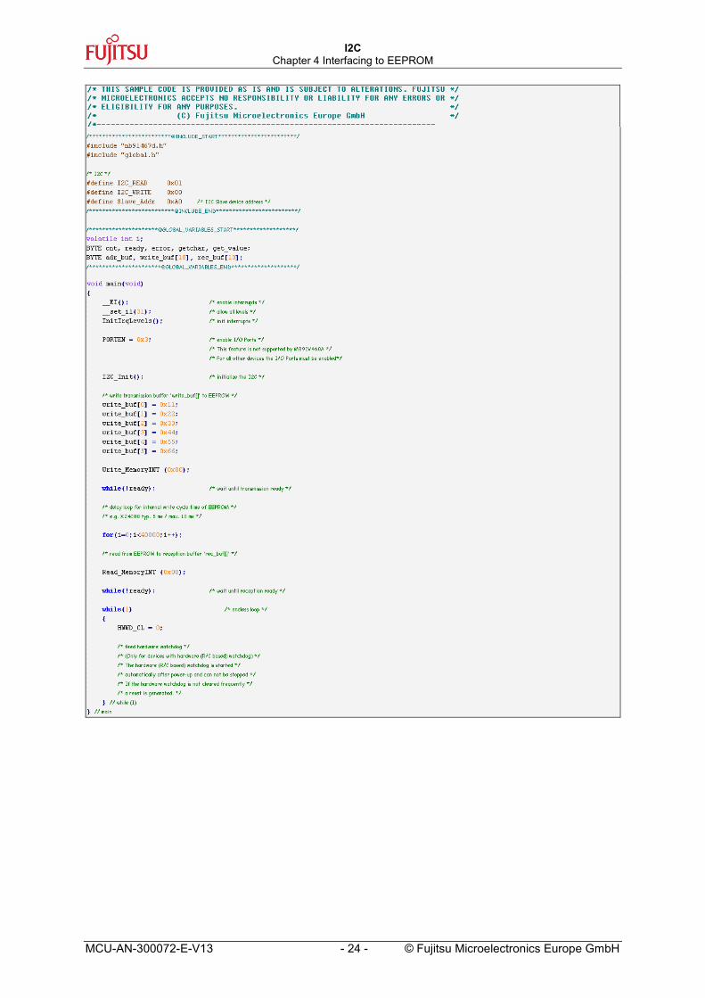
4.4.4.3 Code
I2C Chapter 4 Interfacing to EEPROM
© Fujitsu Microelectronics Europe GmbH - 23 - MCU-AN-300072-E-V13
I2C Chapter 4 Interfacing to EEPROM
MCU-AN-300072-E-V13 - 24 - © Fujitsu Microelectronics Europe GmbH
I2C Chapter 5 Slave mode using Interrupt
© Fujitsu Microelectronics Europe GmbH - 25 - MCU-AN-300072-E-V13
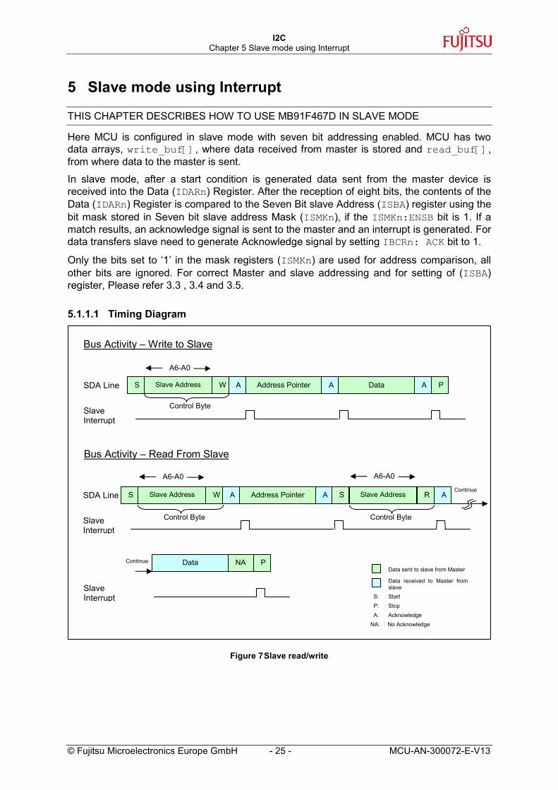
5 Slave mode using Interrupt
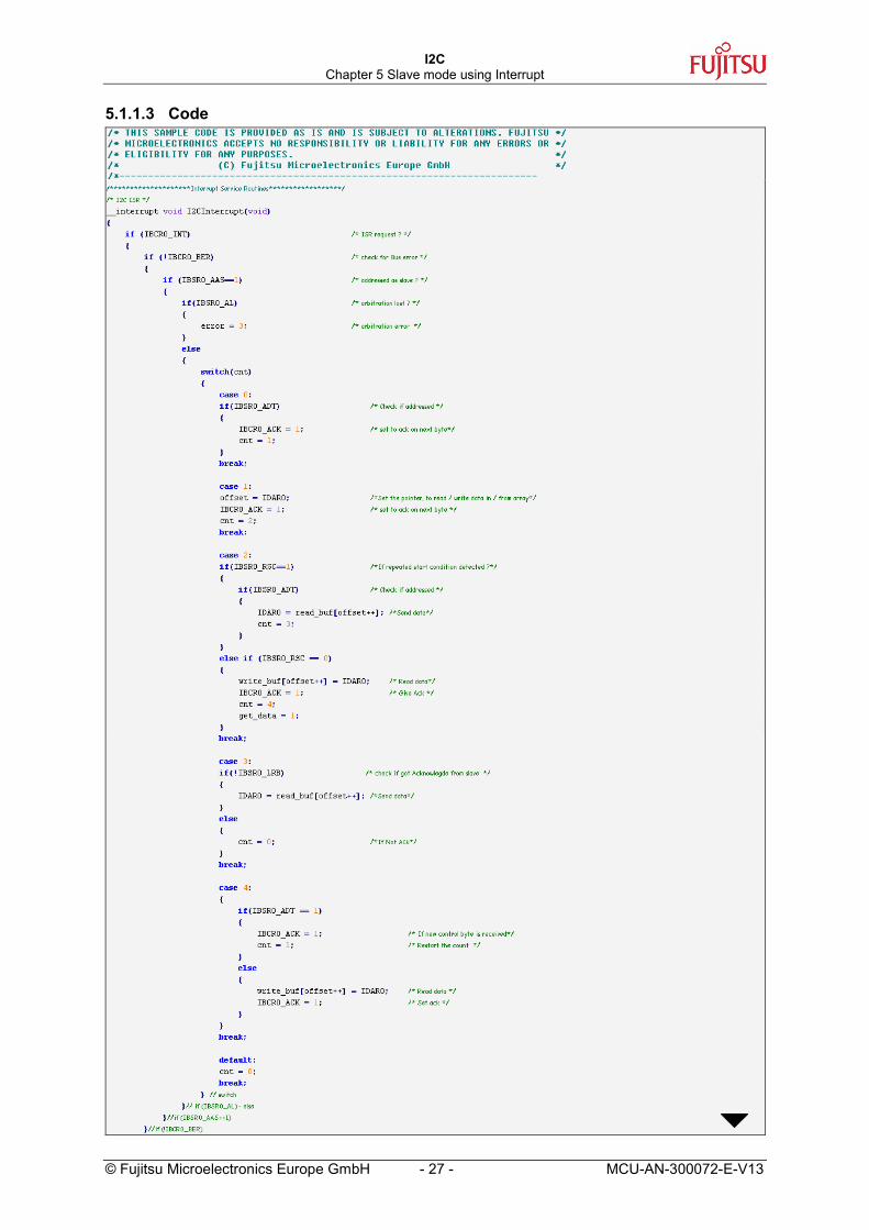
THIS CHAPTER DESCRIBES HOW TO USE MB91F467D IN SLAVE MODE
Here MCU is configured in slave mode with seven bit addressing enabled. MCU has two data arrays, write_buf[], where data received from master is stored and read_buf[],from where data to the master is sent.
In slave mode, after a start condition is generated data sent from the master device is received into the Data (IDARn) Register. After the reception of eight bits, the contents of the Data (IDARn) Register is compared to the Seven Bit slave Address (ISBA) register using the bit mask stored in Seven bit slave address Mask (ISMKn), if the ISMKn:ENSB bit is 1. If a match results, an acknowledge signal is sent to the master and an interrupt is generated. For data transfers slave need to generate Acknowledge signal by setting IBCRn: ACK bit to 1.
Only the bits set to ‘1’ in the mask registers (ISMKn) are used for address comparison, all other bits are ignored. For correct Master and slave addressing and for setting of (ISBA)register, Please refer 3.3 , 3.4 and 3.5.
5.1.1.1 Timing Diagram
Figure 7 Slave read/write
A6-A0
Continue SDA Line
SDA Line
Control Byte
S: Start P: Stop
A: Acknowledge NA: No Acknowledge
Continue
S A Address Pointer A Data A P
Bus Activity – Write to Slave
Slave Interrupt
Slave Address W
S A Address Pointer AW S R
Slave Interrupt
Data NA P
Slave Interrupt
Bus Activity – Read From Slave
Data sent to slave from Master
Data received to Master from slave
A
Control Byte
Slave Address
Control Byte
Slave Address
A6-A0 A6-A0
I2C Chapter 5 Slave mode using Interrupt
MCU-AN-300072-E-V13 - 26 - © Fujitsu Microelectronics Europe GmbH
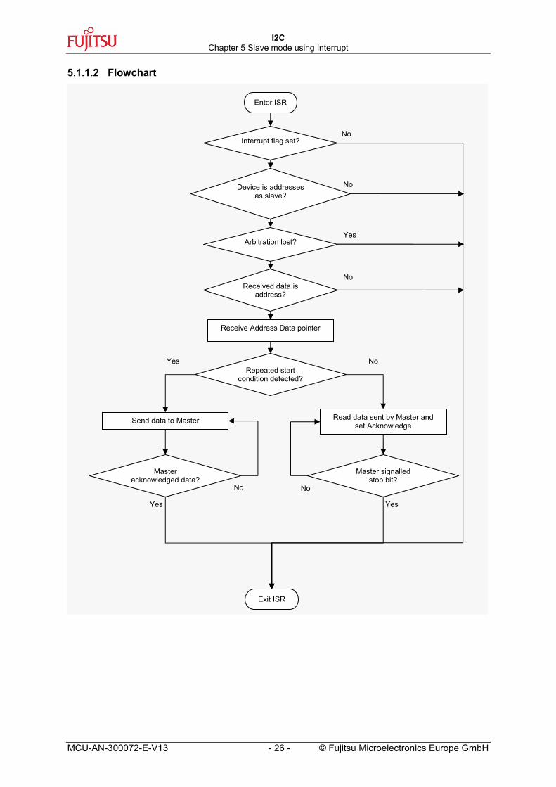
5.1.1.2 Flowchart
Enter ISR
Exit ISR
Interrupt flag set?
Device is addresses as slave?
Arbitration lost?
Received data is address?
Receive Address Data pointer
Repeated start condition detected?
Send data to Master
Master acknowledged data?
Read data sent by Master and set Acknowledge
Master signalled stop bit?
No
No
Yes
No
Yes No
No No
Yes Yes
I2C Chapter 5 Slave mode using Interrupt
© Fujitsu Microelectronics Europe GmbH - 27 - MCU-AN-300072-E-V13
5.1.1.3 Code
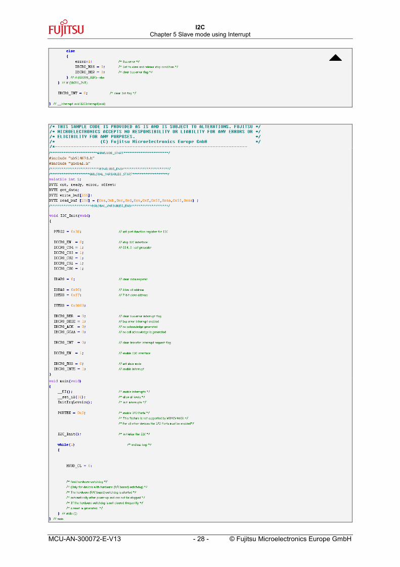
I2C Chapter 5 Slave mode using Interrupt
MCU-AN-300072-E-V13 - 28 - © Fujitsu Microelectronics Europe GmbH
I2C Chapter 6 Appendix
© Fujitsu Microelectronics Europe GmbH - 29 - MCU-AN-300072-E-V13
6 Appendix
6.1 List of Figures Figure 1 Timing Diagram........................................................................................................ 6 Figure 2 Pin Diagram of EEPROM 24LC04.......................................................................... 12 Figure 3 Connection block diagram...................................................................................... 12 Figure 4 Byte write ............................................................................................................... 14 Figure 5 Random Read ........................................................................................................ 17 Figure 6 Master read/write.................................................................................................... 20 Figure 7 Slave read/write...................................................................................................... 25
6.2 List of Tables Table 1 Pin names of EEPROM 24LC04.............................................................................. 12
I2C Chapter 7 Additional Information
MCU-AN-300072-E-V13 - 30 - © Fujitsu Microelectronics Europe GmbH
7 Additional Information Information about FUJITSU Microcontrollers can be found on the following Internet page:
http://mcu.emea.fujitsu.com/
The software examples related to this application note is:
91460_i2c_400khz-v11 91460_i2c_400khz_irq-v10 91460_i2c_400khz_irq_slave-v10 It can be found on the following Internet page:
http://mcu.emea.fujitsu.com/mcu_product/mcu_all_software.htm


![65nm CMOS Process Technology - Fujitsu · 65nm CMOS Process Technology Paul Kim Senior Manager, Foundry Services Fujitsu Microelectronics America, Inc. ... [nm] 0 500 400 300 200](https://img.pdfslide.us/doc/110x75/5c63c41809d3f2ad198bc41b/65nm-cmos-process-technology-65nm-cmos-process-technology-paul-kim-senior.jpg)