Embed Size (px)
Citation preview

©2009 by Matthias Herrmann │ Do not copy or distribute by any means │ For private use only │ www.FONITRONIK.de
31.01.2011
The VCPS-8 is a sequencer providing one channel of gates, triggers and CV. For control there is a clock in, manual step, manual reset and a reset in. The trigger length follows the pulse width of the incoming clock signal. The reset button is an stop/reset and inhibits the sequencer as long as pushed. However the reset input creates a short reset pulse from the incoming reset gate/pulse signal to prevent the sequencer from stopping. This comes in handy when resetting the sequencer using a divider. Think about it…And then there is a section to provide voltage control of the gate/trigger patterns: CV in, manual pattern select (offset/fine), and two LEDs indicating the limits of the CV (<0V and >5V). The patterns of the 8 steps are under the control of an ADC, however each step can be set manually too, to overwrite the ADC pattern if desired.
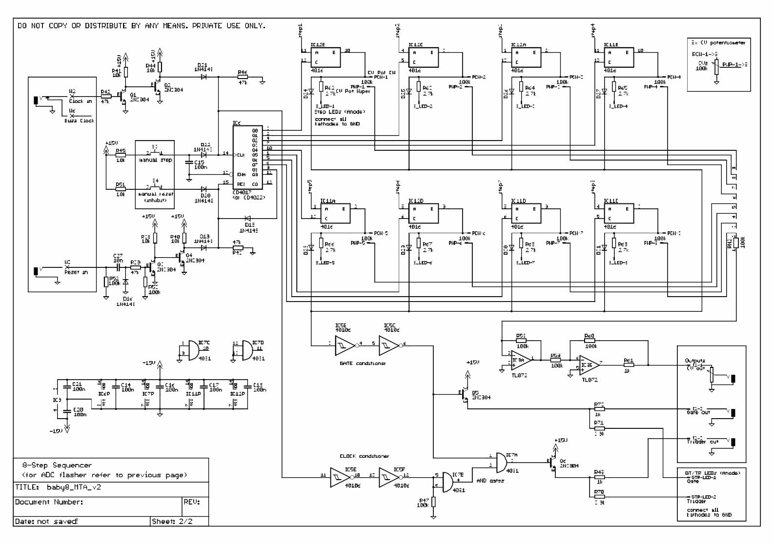
Some time ago a kind fellow sent me some old EFM schematics to upload them to my site. One was the ADC flash, based on LED driver ICs (LM3915). I thought about the use for an ADC module for a modular synthesizer and came up with the idea of controlling the steps of a sequencer with it. But why use expensive or hard to get LM3914/15? so I utilized an ADC0801 (or even 0804) for that purpose. This IC accepts 0V-5V input, so i put a simple CV processor upfront the ADC, with two additional comparators to drive indicator LEDs for voltages >5VA or <0C. The outputs of the ADC are converted to grey code (4030) and amplified (TL074). The 4017 based sequencer then switches these voltage on/off (4016). Each step can be manually controlled by a switch, selecting on-off-ADC - so one could overwrite the ADC. The actual sequencer section is a common 4017 based design. However I utilized inverted schmitt triggers (40106) and AND gates (4081) to create a trigger from the incoming clock and the gates of the sequencer.There are 20 LEDs: 8 for showing the pattern of the ADC, 8 LEDs showing the actual active steps, 2 LEDs for the CV processor, and 2 ELDs for the gate and trigger outputs.
To the left you can see my two builts of the sequencer, one 1U stand alone unit, and one eurorack module.
Voltage Controlled Pattern Sequencer VCPS-8
©2009 by Matthias Herrmann │ Do not copy or distribute by any means │ For private use only │ www.FONITRONIK.de
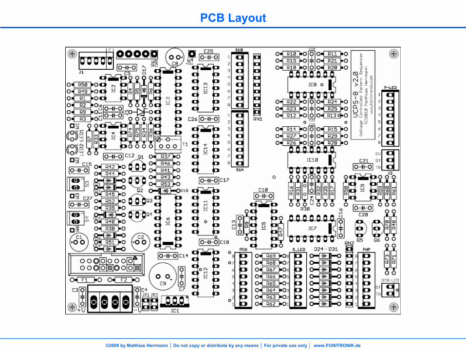
PCB Layout
©2009 by Matthias Herrmann │ Do not copy or distribute by any means │ For private use only │ www.FONITRONIK.de
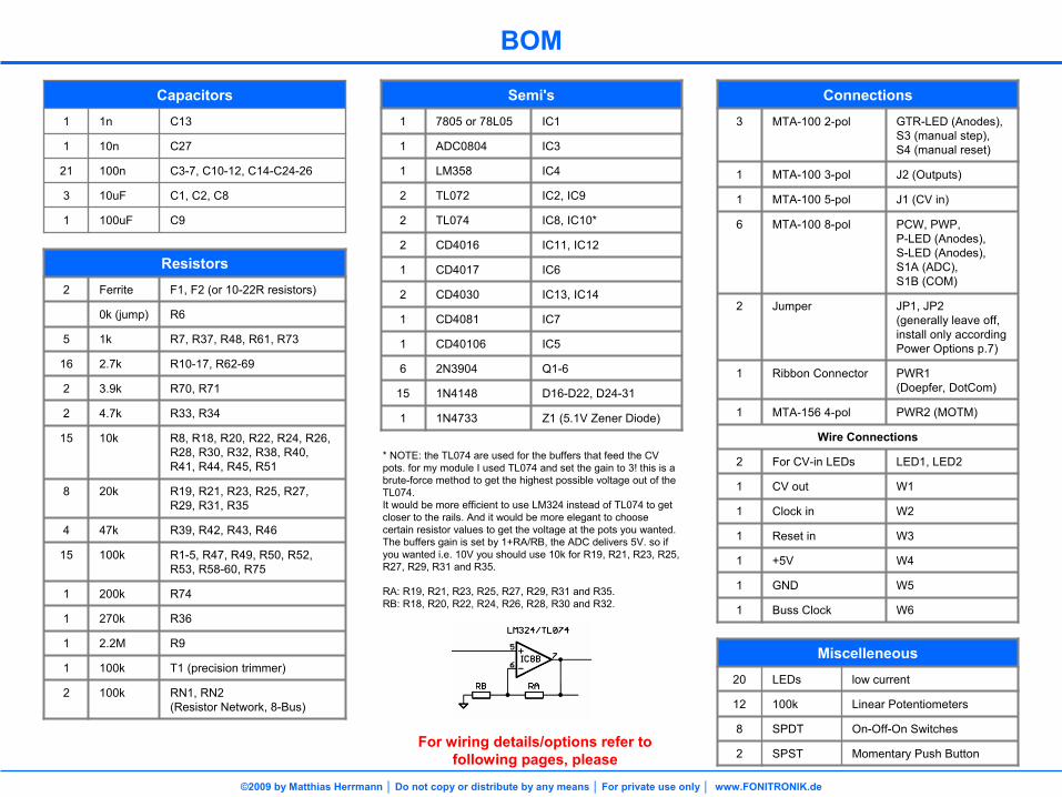
BOM
Resistors2 Ferrite F1, F2
(or 10-22R resistors)
0k (jump) R6
5 1k R7, R37, R48, R61, R73
16 2.7k R10-17, R62-69
2 3.9k R70, R71
2 4.7k R33, R34
15 10k R8, R18, R20, R22, R24, R26, R28, R30, R32, R38, R40, R41, R44, R45, R51
8 20k R19, R21, R23, R25, R27, R29, R31, R35
4 47k R39, R42, R43, R46
15 100k R1-5, R47, R49, R50, R52, R53, R58-60, R75
1 200k R74
1 270k R36
1 2.2M R9
1 100k T1
(precision trimmer)
2 100k RN1, RN2
(Resistor
Network, 8-Bus)
Semi's1 7805
or 78L05 IC1
1 ADC0804 IC3
1 LM358 IC4
2 TL072 IC2, IC9
2 TL074 IC8, IC10*
2 CD4016 IC11, IC12
1 CD4017 IC6
2 CD4030 IC13, IC14
1 CD4081 IC7
1 CD40106 IC5
6 2N3904 Q1-6
15 1N4148 D16-D22, D24-31
1 1N4733 Z1
(5.1V Zener Diode)
Connections3 MTA-100 2-pol GTR-LED (Anodes),
S3
(manual step),S4
(manual reset)
1 MTA-100 3-pol J2
(Outputs)
1 MTA-100 5-pol J1
(CV in)
6 MTA-100 8-pol PCW, PWP,
P-LED (Anodes),
S-LED (Anodes),S1A (ADC),
S1B (COM)
2 Jumper JP1, JP2(generally leave off, install only according Power Options p.7)
1 Ribbon Connector PWR1
(Doepfer, DotCom)
1 MTA-156 4-pol PWR2
(MOTM)
Wire Connections
2 For CV-in LEDs LED1, LED2
1 CV out W1
1 Clock in W2
1 Reset in W3
1 +5V W4
1 GND W5
1 Buss Clock W6
Capacitors1 1n C13
1 10n C27
21 100n C3-7, C10-12, C14-C24-26
3 10uF C1, C2, C8
1 100uF C9
Miscelleneous20 LEDs low current
12 100k Linear Potentiometers
8 SPDT On-Off-On Switches
2 SPST Momentary Push ButtonFor wiring details/options refer to
following pages, please
* NOTE: the TL074 are used for the buffers that feed the CV pots. for my module I used TL074 and set the gain to 3! this is a brute-force method to get the highest possible voltage out of the TL074.It would be more efficient to use LM324 instead of TL074 to get closer to the rails. And it would be more elegant to choose certain resistor values to get the voltage at the pots you wanted.The buffers gain is set by 1+RA/RB, the ADC delivers 5V. so if you wanted i.e. 10V you should use 10k for R19, R21, R23, R25, R27, R29, R31 and R35.
RA: R19, R21, R23, R25, R27, R29, R31 and R35.RB: R18, R20, R22, R24, R26, R28, R30 and R32.

06.07.2010
©2009 by Matthias Herrmann │ Do not copy or distribute by any means │ For private use only │ www.FONITRONIK.de
ADC Wiring (CV Processor & Pattern LEDs)
(J1 offers two additional CV inputs on pins 2 & 4)
These LEDs show the active pattern, set by the ADC and the switches)

©2009 by Matthias Herrmann │ Do not copy or distribute by any means │ For private use only │ www.FONITRONIK.de
Switches Wiring & Clock/Reset Wiring
Pattern Programmer ON-OFF-ON Switches Step/Reset Momentary Switches
W6
can alternatively be used to feed the Doepfer Buss with the Sequencers Gate or Trigger output (see Output Wiring)
Using these switches you select the mode for each step: On, Off,
or ADC controlled. Please note that for toggle switches the middle pin is conencted to the lower pin when the toggle is high, and vise versa.With these Switches you are able to overwrite the ADC set pattern.

©2009 by Matthias Herrmann │ Do not copy or distribute by any means │ For private use only │ www.FONITRONIK.de
CV Potentiometer Wiring & Step LEDs
Ha ha, nice ball of wool, isn’t it? Seriously, the wiring of the
potentiometers is straight forward. Just connect the pins of the PCW connector to the corrsponding potentiometers CW-pin, and the pins of the PWP connector to the potentiometers wiper pins. I emphasized potentiometer 5 for more clarity. the potentiometers CCW pins shall be connected to one of the GND pads (upper left corner of the PCB).BTW don’t mind the order of the potentiometers in the diagram, it’s just a diagram…
These LEDs indicate the currently active step (depen-
ding on Pattern/Switch setting and clock). I would choose a different color than the Pattern LEDs.
GND

©2009 by Matthias Herrmann │ Do not copy or distribute by any means │ For private use only │ www.FONITRONIK.de
Output Wiring & Power Setup Options
W6
can alternatively be used to feed the Doepfer Buss with the Sequencers Gate or Trigger output (see Clock/Reset Wiring)
Doepfer Style Connector+12V
/ GND
/
-12V+5V: if you wanted to use the Doepfer
Buss 5V line close jumper JP1 and leave off voltage regulator IC1. If not, install IC1
to have onboard +5V source.Pins 15, 16 (Gate Buss) are connected
to pad W6.Important:
for 12V operation change R74 to 150k, R75 to 110k (the R74/R75
voltage divider shall give you 5V)
DotCom Style Connector+15V
/
GND
/
-15V+5V: if you wanted to use the
DotCom Buss 5V line close jumper JP2 and leave off voltage regulator IC1. If not, install IC1 to
have onboard +5V source.
MOTM Style Connector+15V
/
GND
/
-15Vnothing special to take care about.

©2009 by Matthias Herrmann │ Do not copy or distribute by any means │ For private use only │ www.FONITRONIK.de
Calibration of the ADC & Graycode
As said before the A output of the ADC is converted from common HEX code to Gray code, For more information about Gray code you may want to refer to http://en.wikipedia.org/wiki/Gray_code. For now it is enough to know that for Gray code two successive values differ in only one bit. This will result in less errors, and that’s why we use it here.To the left we see the first and the last 16 patterns of an 8-bit Gray code, and these will be the patterns you can address using external CV or the manual controls. For the complete table refer to http://www.modular.fonik.de/pdf/8-
bitGraycode.pdf.
To be able to address all 256 patterns you need to calibrate the
reference voltage of the ADC, using trimmer T1. Proceed as follows:
1.
Set all pattern switches to ADC mode.2.
Turn the Offset control to the right until the >5V indication LED is lit.
This means that the maximum voltage is fed to the ADC input.
3.
Turn T1 until only the last pattern LED is lit.
You now dialed in the last pattern. In the beginning the Gray code will be a little bit confusing, however you will get used to it after a while.

©2009 by Matthias Herrmann │ Do not copy or distribute by any means │ For private use only │ www.FONITRONIK.de
Wiring the VCPS-8 as simple 8-step Sequencer
This is the simple and straight forward method. You just leave off the complete ADC part of the circuitry, and use on-off
switches instead of the on-off-on for S1A&B.
Bridge C13 to tie the 40106 input to GND!
Option I (not tested)

©2009 by Matthias Herrmann │ Do not copy or distribute by any means │ For private use only │ www.FONITRONIK.de
Wiring the VCPS-8 as simple 8-step Sequencer
This is the more complicated method that will save you a lot of parts, however it requires a little bit of a different wiring. Leave of all parts as you would do for Option I (shaded red), and additionally leave off all parts that are shaded orange. And then the CD4016 Quad Analog Switch ICs (IC11,
IC12) will be replaced by manual switches (refer to next page)!
Again, bridge C13 to tie the 40106 input to GND!
Option II (not tested)

©2009 by Matthias Herrmann │ Do not copy or distribute by any means │ For private use only │ www.FONITRONIK.de
Wiring the VCPS-8 as simple 8-step Sequencer
Option II (cont’d)
contact pin of switch
Step IC11 pin IC12 pin
1 12
2 5
3 13
4 12
5 13
6 6
7 6
8 5
COM pin of switch
Step IC11 pin IC12 pin
1 10
2 3
3 2
4 10
5 2
6 9
7 9
8 3
or as tables:

©2009 by Matthias Herrmann │ Do not copy or distribute by any means │ For private use only │ www.FONITRONIK.de
Automatic ADC Ignition System
Some people experienced issues with the ADC when using certain PSU’s. The ADC simply did not start the conversion when the module was powered up. As soon as they changed the PSU it did.
Anyways, the cicuit below should force the ADC to start conversion in these cases.
When the module get’s powered up, a short pulse is created from the rising edge of the +5V rail. This pulse controlls a transistor, which shorts pins 3 & 5 of the DAC momentarily to GND.


![0804 EAV (CFA610)[1]](https://img.pdfslide.us/doc/110x75/577d39a41a28ab3a6b9a3fc6/0804-eav-cfa6101.jpg)


![Manual Type25USM 0804[1]](https://img.pdfslide.us/doc/110x75/577d24541a28ab4e1e9c33f4/manual-type25usm-08041.jpg)