Embed Size (px)
Citation preview

3.0 A, 15 V, Step-Down
Switching Regulator
The LM2576 series of regulators are monolithic integrated circuits ideally suited for easy and convenient design of a step–down switching regulator (buck converter). All circuits of this series are capable of driving a 3.0 A load with excellent line and load regulation. These devices are available in fixed output voltages of 3.3 V, 5.0 V, 12 V, 15 V, and an adjustable output version.
These regulators were designed to minimize the number of external components to simplify the power supply design. Standard series of inductors optimized for use with the LM2576 are offered by several different inductor manufacturers. Since the LM2576 converter is a switch–mode power supply, its efficiency is significantly higher in comparison with popular three–terminal linear regulators, especially with higher input voltages. In many cases, the power dissipated is so low that no heatsink is required or its size could be reduced dramatically.
TO-220-5L
TO-263-5L
A standard series of inductors optimized for use with the LM2576 are available from several different manufacturers. This feature greatly simplifies the design of switch–mode power supplies. The LM2576 features include a guaranteed ±4% tolerance on output voltage within specified input voltages and output load conditions, and ±10% on the oscillator frequency (±2% over 0°C to 125°C). External shutdown is included, featuring 80 ㎂ (typical) standby current. The output switch includes cycle–by–cycle current limiting, as well as thermal shutdown for full protection under fault conditions.
Features 3.3 V, 5.0 V, 12 V, 15 V, and Adjustable Output Versions Adjustable Version Output Voltage Range, 1.23 to 37 V ±4% Maximum Over Line and Load Conditions Guaranteed 3.0 A Output Current Wide Input Voltage Range Requires Only 4 External Components 52 kHz Fixed Frequency Internal Oscillator TTL Shutdown Capability, Low Power Standby Mode High Efficiency Uses Readily Available Standard Inductors Thermal Shutdown and Current Limit Protection
Applications Simple High–Efficiency Step–Down (Buck) Regulator Efficient Pre–Regulator for Linear Regulators On–Card Switching Regulators Positive to Negative Converter (Buck–Boost) Negative Step–Up Converters Power Supply for Battery Chargers
Pin connections
1. Vin 2. Output 3. Ground 4. Feedback 5. ON/OFF
ORDERING INFORMATION
Device Operating
Temperature Range Package Packing
LM2576SXX TA = -40 to 125 C
for all packages
TO-263 Tape & Reel
LM2576TXX TO-220 Tube
LM2576-xx
LM2576-xx
LM2576T
LM2576S
1Shenzhen H&M Semiconductor Co.Ltd http://www.hmsemi.com

LM2576-xx
Typical Application (Fixed Output Voltage Versions)
Figure 1.
Representative Block Diagram and Typical Application
This device contains 162 active transistors.
Figure 2. ABSOLUTE MAXIMUM RATINGS
(Absolute Maximum Ratings indicate limits beyond which damage to the device may occur.)
Rating Symbol Value Unit Maximum Supply Voltage Vin 45 V ON/OFF Pin Input Voltage – –0.3 V V +Vin V Output Voltage to Ground (Steady–State) – –1.0 V Power Dissipation TO–220, 5–Lead Thermal Resistance, Junction–to–Ambient Thermal Resistance, Junction–to–Case TO–263, 5–Lead (D2PAK) Thermal Resistance, Junction–to–Ambient Thermal Resistance, Junction–to–Case
PD RθJA RθJC PD RθJA RθJC
Internally Limited 65 5.0 Internally Limited 70 5.0
W °C/W °C/W W °C/W °C/W
Storage Temperature Range Tstg –65 to +150 °C Minimum ESD Rating (Human Body Model: C = 100 pF, R = 1.5 kΩ)
– 2.0 kV
Lead Temperature (Soldering, 10 seconds) – 260 °C Maximum Junction Temperature TJ 150 °C
* Stresses beyond those listed under “absolute maximum ratings” may cause permanent damage to the device. These are stress ratings only and functional operation of the device at these or any other conditions beyond those indicated under “recommended operating conditions” is not implied. Exposure to absolute-maximum-rated conditions for extended periods may affect device reliability.
2Shenzhen H&M Semiconductor Co.Ltd http://www.hmsemi.com

OPERATING RATINGS
(Operating Ratings indicate conditions for which the device is intended to be functional, but do not guarantee specific performance limits. For guaranteed specifications and test conditions, see the Electrical Characteristics.)
Rating Symbol Value Unit Operating Junction Temperature Range TJ –40 to +125 °C Supply Voltage Vin 40 V
SYSTEM PARAMETERS [Note 1] ELECTRICAL CHARACTERISTICS (Unless otherwise specified, Vin = 12 V for the 3.3 V, 5.0 V, and Adjustable version, Vin = 25 V for the 12 V version, and Vin = 30 V for the 15 V version. ILoad = 500 mA, TJ = 25°C, for min/max values TJ is the operating junction temperature range that applies [Note 2], unless otherwise noted.)
Characteristics Symbol Min Max Unit
([Note 1] Test Circuit Figure 3) Output Voltage Vout 3.234 3.366 V Output Voltage (6.0 V Vin 40 V, 0.5 A ILoad 3.0 A) TJ = 25°C TJ = –40 to +125°C
Vout 3.168 3.135
3.432 3.465
V
Efficiency (Vin = 12 V, ILoad = 3.0 A) 65 - %
[Note 1] Output Voltage Vout 4.9 5.1 V Output Voltage (8.0 V Vin 40 V, 0.5 A ILoad 3.0 A) TJ = 25°C TJ = –40 to +125°C
Vout 4.8 4.75
5.2 5.25
V
Efficiency (Vin = 12 V, ILoad = 3.0 A) 67 - % [Note 1]
Output Voltage Vout 11.76 12.24 V Output Voltage (15.0 V Vin 40 V, 0.5 A ILoad 3.0 A) TJ = 25°C TJ = –40 to +125°C
Vout 11.52 11.4
12.48 12.6
V
Efficiency (Vin = 12 V, ILoad = 3.0 A) 78 - %
Output Voltage Vout 14.7 15.3 V Output Voltage (18 V Vin 40 V, 0.5 A ILoad 3.0 A) TJ = 25°C TJ = –40 to +125°C
Vout 14.4 14.25
15.6 15.75
V
Efficiency (Vin = 12 V, ILoad = 3.0 A) 78 - % ADJUSTABLE VERSION [Note 1]
Feedback Voltage (Vin = 12 V, ILoad = 0.5 A, Vout = 5.0 V, TJ = 25°C)
Vout 1.217 1.243 V
Feedback Voltage (8.0 V Vin 40 V, 0.5 A ILoad 3.0 A, Vout = 5.0 V) TJ = 25°C TJ = –40 to +125°C
Vout 1.193 1.18
1.267 1.28
V
Efficiency (Vin = 12 V, ILoad = 3.0 A, Vout = 5.0 V) 67 - % 1. External components such as the catch diode, inductor, input and output capacitors can affect switching regulator system performance. When the LM2576 is used as shown in the test circuit, system performance will be as shown in system parameters section . 2. Tested junction temperature range for the LM2576: Tlow = –40°C Thigh = +125°C
LM2576-xx
LM2576-3.3
LM2576-5
LM2576-12
[Note 1] LM2576-15
LM2576
3Shenzhen H&M Semiconductor Co.Ltd http://www.hmsemi.com

DEVICE PARAMETERS
ELECTRICAL CHARACTERISTICS (Unless otherwise specified, Vin = 12 V for the 3.3 V, 5.0 V, and Adjustable version, Vin = 25 V for the 12 V version, and Vin = 30 V for the 15 V version. ILoad = 500 mA, TJ = 25°C, for min/max values TJ is the operating junction temperature range that applies [Note 2], unless otherwise noted.)
Characteristics Symbol Min Max Unit ALL OUTPUT VOLTAGE VERSIONS Feedback Bias Current (Vout = 5.0 V [Adjustable Version Only]) TJ = 25°C TJ = –40 to +125°C
Ib – –
100 500
nA
Oscillator Frequency [Note 3] TJ = 25°C TJ = –40 to +125°C
fosc – 42
– 63
kHz
Saturation Voltage (Iout = 3.0 A [Note 4]) TJ = 25°C TJ = –40 to +125°C
Vsat – –
1.8 2.0
V
Max Duty Cycle (“on”) [Note 5] DC 93 – % Current Limit (Peak Current [Notes 3 and 4]) TJ = 25°C TJ = –40 to +125°C
ICL 4.2 3.5
6.9 7.5
A
Output Leakage Current [Notes 6 and 7], TJ = 25°C Output = 0 V Output = –1.0 V
IL – –
2.0 30
mA
Quiescent Current [Note 6] TJ = 25°C TJ = –40 to +125°C
IQ – –
10 11
mA
Standby Quiescent Current (ON/OFF Pin = 5.0 V (“off”)) TJ = 25°C
Istby –
200
uA
ON/OFF Pin Logic Input Level Vout = 0 V TJ = 25°C TJ = –40 to +125°C Vout = Nominal Output Voltage TJ = 25°C TJ = –40 to +125°C
VIH VIL
2.2 2.4 – –
– – 1.0 0.8
V
ON/OFF Pin Input Current ON/OFF Pin = 5.0 V (“off”), TJ = 25°C ON/OFF Pin = 0 V (“on”), TJ = 25°C
IIH IIL
– –
30 10
uA
3. The oscillator frequency reduces to approximately 18 kHz in the event of an output short or an overload which causes the regulated output voltage to drop approximately 40% from the nominal output voltage. This self protection feature lowers the average dissipation of the IC by lowering the minimum duty cycle from 5% down to approximately 2%. 4. Output (Pin 2) sourcing current. No diode, inductor or capacitor connected to output pin. 5. Feedback (Pin 4) removed from output and connected to 0 V. 6. Feedback (Pin 4) removed from output and connected to +12 V for the Adjustable, 3.3 V, and 5.0 V versions, and +25 V for the 12 V and 15 V versions, to force the output transistor “off”. 7. Vin = 40 V.
LM2576-xx
4Shenzhen H&M Semiconductor Co.Ltd http://www.hmsemi.com

Fixed Output Voltage Versions
Figure 3. Cin – 100 mF, 75 V, Aluminium Electrolytic Cout – 1000 mF, 25 V, Aluminium Electrolytic D1 – Schottky, MBR360 L1 – 100 mH, Pulse Eng. PE–92108 R1 – 2.0 k, 0.1% R2 – 6.12 k, 0.1% Adjustable Output Voltage Versions
Figure 4.
1
20.1R
RVV refout ,
0.112
ref
out
V
VRR
Where Vref = 1.23 V, R1 between 1.0 k and 5.0 k C1 = 10 nF C2 = 1 nF
LM2576-xx
5Shenzhen H&M Semiconductor Co.Ltd http://www.hmsemi.com
Application Information INVERTING REGULATOR
Figure 5 shows a LM2576-12 in a buck-boost configuration to generate a negative 12V output from a positive input voltage. This circuit bootstraps the regulator’s ground pin to the negative output voltage, then by grounding the feedback pin, the regulator senses the inverted output voltage and regulates it to −12V.
For an input voltage of 12V or more, the maximum available output current in this configuration is approximately 700 mA. At lighter loads, the minimum input voltage required drops to approximately 4.7V.
The switch currents in this buck-boost configuration are higher than in the standard buck-mode design, thus lowering the available output current. Also, the start-up input current of the buck-boost converter is higher than the standard buck-mode regulator, and this may overload an input power source with a current limit less than 5A. Using a delayed turn-on or an undervoltage lockout circuit (described in the next section) would allow the input voltage to rise to a high enough level before the switcher would be allowed to turn on.
Because of the structural differences between the buck and the buck-boost regulator topologies, the buck regulator design procedure section can not be used to to select the inductor or the output capacitor. The recommended range of inductor values for the buck-boost design is between 68 µH and 220 µH, and the output capacitor values must be larger than what is normally required for buck designs. Low input voltages or high output currents require a large value output capacitor (in the thousands of micro Farads).
The peak inductor current, which is the same as the peak switch current, can be calculated from the following formula:
Where fosc = 52 kHz. Under normal continuous inductor current operating conditions, the minimum VIN represents the
worst case. Select an inductor that is rated for the peak current anticipated.
FIGURE 5. Inverting Buck-Boost Develops −12V
Also, the maximum voltage appearing across the regulator is the absolute sum of the input and output voltage. For a
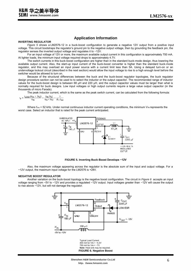
−12V output, the maximum input voltage for the LM2576 is +28V. NEGATIVE BOOST REGULATOR
Another variation on the buck-boost topology is the negative boost configuration. The circuit in Figure 6 accepts an input voltage ranging from −5V to −12V and provides a regulated −12V output. Input voltages greater than −12V will cause the output to rise above −12V, but will not damage the regulator.
Typical Load Current 400 mA for VIN = −5.2V 750 mA for VIN = −7V Note: Heat sink may be required.
FIGURE 6. Negative Boost
LM2576-xx
6Shenzhen H&M Semiconductor Co.Ltd http://www.hmsemi.com

Because of the boosting function of this type of regulator, the switch current is relatively high, especially at low input
voltages. Output load current limitations are a result of the maximum current rating of the switch. Also, boost regulators can not
provide current limiting load protection in the event of a shorted load, so some other means (such as a fuse) may be necessary. UNDERVOLTAGE LOCKOUT
In some applications it is desirable to keep the regulator off until the input voltage reaches a certain threshold. An undervoltage lockout circuit which accomplishes this task is shown in Figure 7 while Figure 8 shows the same circuit applied to a buck-boost configuration. These circuits keep the regulator off until the input voltage reaches a predetermined level.
VTH =VZ1 + 2VBE(Q1)
Note: Complete circuit not shown.
FIGURE 7. Undervoltage Lockout for Buck Circuit
Note: Complete circuit not shown (see Figure 10).
FIGURE 8. Undervoltage Lockout for Buck-Boost Circuit
DELAYED STARTUP The ON /OFF pin can be used to provide a delayed startup feature as shown in Figure 9. With an input voltage of 20V and for the part values shown, the circuit provides approximately 10 ms of delay time before the circuit begins switching. Increasing the RC time constant can provide longer delay times. But excessively large RC time constants can cause problems with input voltages that are high in 60 Hz or 120 Hz ripple, by coupling the ripple into the ON /OFF pin.
Note: Complete circuit not shown.
FIGURE 9. Delayed Startup
LM2576-xx
7Shenzhen H&M Semiconductor Co.Ltd http://www.hmsemi.com

ADJUSTABLE OUTPUT, LOW-RIPPLE POWER SUPPLY A 3A power supply that features an adjustable output voltage is shown in Figure 10. An additional L-C filter that reduces the output ripple by a factor of 10 or more is included in this circuit.
FIGURE 10. Adjustable 3A Power Supply with Low Output Ripple Definition of Terms
BUCK REGULATOR A switching regulator topology in which a higher voltage is converted to a lower voltage. Also known as a step-down switching regulator. BUCK-BOOST REGULATOR A switching regulator topology in which a positive voltage is converted to a negative voltage without a transformer. DUTY CYCLE (D) Ratio of the output switch’s on-time to the oscillator period.
CATCH DIODE OR CURRENT STEERING DIODE The diode which provides a return path for the load current when the LM2576 switch is OFF. EFFICIENCY () The proportion of input power actually delivered to the load.
LM2576-xx
8Shenzhen H&M Semiconductor Co.Ltd http://www.hmsemi.com

TO-220-5L
LM2576-xx
9Shenzhen H&M Semiconductor Co.Ltd http://www.hmsemi.com

TO-263-5L
LM2576-xx
10Shenzhen H&M Semiconductor Co.Ltd http://www.hmsemi.com