Embed Size (px)
Citation preview

This is information on a product in full production.
January 2018 DocID11703 Rev 6 1/41
TS4962M
3 W filter-free class D audio power amplifier
Datasheet - production data
Features• Operating from VCC = 2.4 V to 5.5 V
• Standby mode active low
• Output power: 3 W into 4 Ω and 1.75 W into 8 Ω with 10% THD+N max. and 5 V power supply
• Output power: 2.3 W @5 V or 0.75 W @ 3.0 V into 4 Ω with 1% THD+N max.
• Output power: 1.4 W @5 V or 0.45 W @ 3.0 V into 8 Ω with 1% THD+N max.
• Adjustable gain via external resistors
• Low current consumption 2 mA @ 3 V
• Efficiency: 88% typ.
• Signal to noise ratio: 85 dB typ.
• PSRR: 63 dB typ. @217 Hz with 6 dB gain
• PWM base frequency: 250 kHz
• Low pop and click noise
• Thermal shutdown protection
• Available in Flip Chip 9 x 300 µm (Pb-free)
Related products• See TS2007 for further gain settings e.g.
6 or 12 dB
• See TS2012 for stereo settings
Applications• Portable gaming consoles
• VR headsets
• Smart phones
• Tablets
DescriptionThe TS4962M is a differential Class-D BTL power amplifier. It is able to drive up to 2.3 W into a 4 Ω load and 1.4 W into a 8 Ω load at 5 V. It achieves outstanding efficiency (88% typ.) compared to classical Class-AB audio amps.
The gain of the device can be controlled via two external gain-setting resistors. Pop and click reduction circuitry provides low on/off switch noise while allowing the device to start within 5 ms. A standby function (active low) allows the reduction of current consumption to 10 nA typ.
www.st.com

Contents TS4962M
2/41 DocID11703 Rev 6
Contents
1 Block diagram and pinout . . . . . . . . . . . . . . . . . . . . . . . . . . . . . . . . . . . . 3
2 Application component information . . . . . . . . . . . . . . . . . . . . . . . . . . . . 4
3 Absolute maximum ratings . . . . . . . . . . . . . . . . . . . . . . . . . . . . . . . . . . . 5
4 Electrical characteristics . . . . . . . . . . . . . . . . . . . . . . . . . . . . . . . . . . . . . 6
5 Electrical characteristic curves . . . . . . . . . . . . . . . . . . . . . . . . . . . . . . . 17
6 Application information . . . . . . . . . . . . . . . . . . . . . . . . . . . . . . . . . . . . . 28
6.1 Differential configuration principle . . . . . . . . . . . . . . . . . . . . . . . . . . . . . . 28
6.2 Gain in typical application schematic . . . . . . . . . . . . . . . . . . . . . . . . . . . . 28
6.3 Common-mode feedback loop limitations . . . . . . . . . . . . . . . . . . . . . . . . 29
6.4 Low frequency response . . . . . . . . . . . . . . . . . . . . . . . . . . . . . . . . . . . . . 29
6.5 Decoupling of the circuit . . . . . . . . . . . . . . . . . . . . . . . . . . . . . . . . . . . . . . 30
6.6 Wake-up time (tWU) . . . . . . . . . . . . . . . . . . . . . . . . . . . . . . . . . . . . . . . . . 30
6.7 Shutdown time (tSTBY) . . . . . . . . . . . . . . . . . . . . . . . . . . . . . . . . . . . . . . . 30
6.8 Consumption in shutdown mode . . . . . . . . . . . . . . . . . . . . . . . . . . . . . . . 30
6.9 Single-ended input configuration . . . . . . . . . . . . . . . . . . . . . . . . . . . . . . . 31
6.10 Output filter considerations . . . . . . . . . . . . . . . . . . . . . . . . . . . . . . . . . . . . 32
6.11 Different examples with summed inputs . . . . . . . . . . . . . . . . . . . . . . . . . . 33
7 Evaluation board . . . . . . . . . . . . . . . . . . . . . . . . . . . . . . . . . . . . . . . . . . . 35
8 Package information . . . . . . . . . . . . . . . . . . . . . . . . . . . . . . . . . . . . . . . . 37
8.1 9-bump Flip Chip package information . . . . . . . . . . . . . . . . . . . . . . . . . . . 37
9 Ordering information . . . . . . . . . . . . . . . . . . . . . . . . . . . . . . . . . . . . . . . 39
10 Revision history . . . . . . . . . . . . . . . . . . . . . . . . . . . . . . . . . . . . . . . . . . . 40

DocID11703 Rev 6 3/41
TS4962M Block diagram and pinout
41
1 Block diagram and pinout
Figure 1. Block diagram
Figure 2. Pinout (top view)
1. Legend: IN+ = positive differential input IN- = negative differential input VDD = analog power supply GND = power supply ground STBY = standby pin (active low) OUT+ = positive differential output OUT- = negative differential output
2. Bumps are underneath, bump diameter = 300 µm
In-
Stdby
In+
Out-
Out+
VccC2
C1
A1
A2
A3
B1 B2
B3
C3
GND
InternalBias
PWM
Output
Bridge
H
Oscillator
150k
150k
+
-
300k

Application component information TS4962M
4/41 DocID11703 Rev 6
2 Application component information
Figure 3. Typical application schematics
Table 1. Component information
Component Functional description
Cs
Bypass supply capacitor. Install as close as possible to the TS4962M to minimize high-frequency ripple. A 100 nF ceramic capacitor should be added to enhance the power supply filtering at high frequency.
RinInput resistor to program the TS4962M differential gain (gain = 300 kΩ/Rin with Rin in kΩ).
Input capacitorDue to common-mode feedback, these input capacitors are optional. However, they can be added to form with Rin a 1st order high-pass filter with -3 dB cut-off frequency = 1/(2*π*Rin*Cin).
Rin
Rin
Cs1u
GND
GND
GND
Vcc
Vcc
SPEAKER
In-
Stdby
In+
Out-
Out+
VccC2
C1
A1
A2
A3
B1 B2
B3
C3
GND
InternalBias
PWM
Output
Bridge
H
Oscillator
150k
150k
+
-
300k
TS4962
capacitorsInput
are optional
+
-
DifferentialInput
In+
GND
In-
GND
Rin
Rin
Cs1u
GND
GND
GND
Vcc
Vcc
+
-
DifferentialInput
capacitorsInput
are optional
In+
GND
In-
GND
2µF
15µH
15µH
Load
4 Ohms LC Output Filter
8 Ohms LC Output Filter
2µF
GND
1µF
30µH
30µH1µF
GND
In-
Stdby
In+
Out-
Out+
VccC2
C1
A1
A2
A3
B1 B2
B3
C3
GND
InternalBias
PWM
Output
Bridge
H
Oscillator
150k
150k
+
-
300k
TS4962

DocID11703 Rev 6 5/41
TS4962M Absolute maximum ratings
41
3 Absolute maximum ratings
Table 2. Absolute maximum ratings
Symbol Parameter Value Unit
VCC Supply voltage (1) (2)
1. Caution: this device is not protected in the event of abnormal operating conditions, such as for example, short-circuiting between any one output pin and ground, between any one output pin and VCC, and between individual output pins.
2. All voltage values are measured with respect to the ground pin.
6V
Vin Input voltage (3)
3. The magnitude of the input signal must never exceed VCC + 0.3 V / GND - 0.3 V.
GND to VCC
Toper Operating free-air temperature range -40 to + 85
°CTstg Storage temperature -65 to +150
Tj Maximum junction temperature 150
Rthja Thermal resistance junction to ambient (4)
4. The device is protected in case of over temperature by a thermal shutdown active @ 150 °C.
200 °C/W
Pdiss Power dissipation Internally limited(5)
5. Exceeding the power derating curves during a long period causes abnormal operation.
ESD Human body model 2 kV
ESD Machine model 200 V
Latch-up Latch-up immunity 200 mA
VSTBY Standby pin voltage maximum voltage (6)
6. The magnitude of the standby signal must never exceed VCC + 0.3 V / GND - 0.3 V.
GND to VCC V
Lead temperature (soldering, 10 s) 260 °C
Table 3. Operating conditions
Symbol Parameter Value Unit
VCC Supply voltage (1)
1. For VCC from 2.4 V to 2.5 V, the operating temperature range is reduced to 0 °C ≤ Tamb ≤ 70 °C.
2.4 to 5.5
VVIC Common-mode input voltage range (2)
2. For VCC from 2.4 V to 2.5 V, the common-mode input range must be set at VCC/2.
0.5 to VCC - 0.8
VSTBY
Standby voltage input: (3)
Device ON Device OFF
3. Without any signal on VSTBY, the device is in standby.
1.4 ≤ VSTBY ≤ VCC GND ≤ VSTBY ≤ 0.4 (4)
4. Minimum current consumption is obtained when VSTBY = GND.
RL Load resistor ≥ 4 Ω
Rthja Thermal resistance junction to ambient (5)
5. With heat sink surface = 125 mm2.
90 °C/W

Electrical characteristics TS4962M
6/41 DocID11703 Rev 6
4 Electrical characteristics
Table 4. VCC = 5 V, GND = 0 V, VIC = 2.5 V, tamb = 25 °C (unless otherwise specified)
Symbol Parameter Conditions Min. Typ. Max. Unit
ICC Supply current No input signal, no load 2.3 3.3 mA
ISTBY Standby current (1) No input signal, VSTBY = GND 10 1000 nA
VOO Output offset voltage No input signal, RL = 8 Ω 3 25 mV
Pout Output power
G=6 dBTHD = 1% max., F = 1 kHz, RL = 4 Ω THD = 10% max., F = 1 kHz, RL = 4 Ω THD = 1% max., F = 1 kHz, RL = 8 Ω THD = 10% max., F = 1 kHz, RL = 8 Ω
2.33
1.41.75
W
THD + NTotal harmonic distortion + noise
Pout = 900 mWRMS, G = 6 dB, 20 Hz < F < 20 kHz RL = 8 Ω + 15 µH, BW < 30 kHz Pout = 1 WRMS, G = 6 dB, F = 1 kHz, RL = 8 Ω + 15 µH, BW < 30 kHz
1
0.4
%
Efficiency EfficiencyPout = 2 WRMS, RL = 4 Ω + ≥ 15 µH Pout =1.2 WRMS, RL = 8 Ω+ ≥ 15 µH
7888
%
PSRRPower supply rejection ratio with inputs grounded (2)
F = 21 Hz, RL = 8 Ω, G=6 dB, Vripple = 200 mVpp
63 dB
CMRRCommon-mode rejection ratio
F = 217 Hz, RL = 8 Ω, G = 6 dB, ΔVicm = 200 mVpp
57 dB
Gain Gain value Rin in kΩ V/V
RSTBYInternal resistance from Standby to GND
273 300 327 kΩ
FPWM Pulse width modulator base frequency
180 250 320 kHz
SNR Signal to noise ratio A-weighting, Pout = 1.2 W, RL = 8 Ω 85 dB
tWU Wake-up time 5 10 ms
tSTBY Standby time 5 10 ms
273kΩRin
------------------ 300kΩRin
------------------ 327kΩRin
------------------

DocID11703 Rev 6 7/41
TS4962M Electrical characteristics
41
VN Output voltage noise
F = 20 Hz to 20 kHz, G = 6 dBUnweighted RL = 4 Ω A-weighted RL = 4 Ω
8560
μVRMS
Unweighted RL = 8 Ω A-weighted RL = 8 Ω
8662
Unweighted RL = 4 Ω + 15 µH A-weighted RL = 4 Ω + 15 µH
8360
Unweighted RL = 4 Ω + 30 µH A-weighted RL = 4 Ω + 30 µH
8864
Unweighted RL = 8 Ω + 30 µH A-weighted RL = 8 Ω + 30 µH
7857
Unweighted RL = 4 Ω + filter A-weighted RL = 4 Ω + filter
8765
Unweighted RL = 4 Ω + filter A-weighted RL = 4 Ω + filter
8259
1. Standby mode is active when VSTBY is tied to GND.
2. Dynamic measurements - 20*log(rms(Vout)/rms(Vripple)). Vripple is the superimposed sinusoidal signal to VCC @ F = 217 Hz.
Table 4. VCC = 5 V, GND = 0 V, VIC = 2.5 V, tamb = 25 °C (unless otherwise specified) (continued)
Symbol Parameter Conditions Min. Typ. Max. Unit

Electrical characteristics TS4962M
8/41 DocID11703 Rev 6
Table 5. VCC = 4.2V, GND = 0V, VIC = 2.5V, Tamb = 25°C (unless otherwise specified) (1)
Symbol Parameter Conditions Min. Typ. Max. Unit
ICC Supply current No input signal, no load 2.1 3 mA
ISTBYStandby current (2) No input signal, VSTBY = GND 10 1000 nA
VOOOutput offset voltage
No input signal, RL = 8 Ω 3 25 mV
Pout Output power
G=6dBTHD = 1% max, F = 1 kHz, RL = 4 Ω THD = 10% max, F = 1 kHz, RL = 4 Ω THD = 1% max, F = 1 kHz, RL = 8 Ω THD = 10% max, F = 1 kHz, RL = 8 Ω
1.62
0.951.2
W
THD + NTotal harmonic distortion + noise
Pout = 600mWRMS, G = 6 dB, 20 Hz < F < 20k Hz RL = 8 Ω + 15 µH, BW < 30 kHz Pout = 700 mWRMS, G = 6 dB, F = 1 kHz, RL = 8 Ω + 15 µH, BW < 30 kHz
1
0.35
%
Efficiency Efficiency
Pout = 1.45 WRMS, RL = 4 Ω + ≥ 15 µH Pout =0.9 WRMS, RL = 8 Ω+ ≥ 15 µH
7888
%
PSRR
Power supply rejection ratio with inputs grounded (3)
F = 217 Hz, RL = 8 Ω, G=6 dB, Vripple = 200 mVpp
63 dB
CMRRCommon-mode rejection ratio
F = 217 Hz, RL = 8 Ω, G = 6 dB, ΔVicm = 200 mVpp
57 dB
Gain Gain value Rin in kΩ V/V
RSTBY
Internal resistance from Standby to GND
273 300 327 kΩ
FPWM Pulse width modulator base frequency
180 250 320 kHz
SNRSignal to noise ratio
A-weighting, Pout = 0.9 W, RL = 8 Ω 85 dB
tWU Wake-uptime 5 10 ms
tSTBY Standby time 5 10 ms
273kΩRin
------------------ 300kΩRin
------------------ 327kΩRin
------------------

DocID11703 Rev 6 9/41
TS4962M Electrical characteristics
41
VNOutput voltage noise
F = 20Hz to 20 kHz, G = 6 dBUnweighted RL = 4 Ω A-weighted RL = 4 Ω
8560
μVRMS
Unweighted RL = 8 Ω A-weighted RL = 8 Ω
8662
Unweighted RL = 4 Ω + 15 µH A-weighted RL = 4 Ω + 15 µH
8360
Unweighted RL = 4 Ω + 30 µH A-weighted RL = 4 Ω + 30 µH
8864
Unweighted RL = 8 Ω + 30 µH A-weighted RL = 8 Ω + 30 µH
7857
Unweighted RL = 4 Ω + filter A-weighted RL = 4 Ω + filter
8765
Unweighted RL = 4 Ω + filter A-weighted RL = 4 Ω + filter
8259
1. All electrical values are guaranteed with correlation measurements at 2.5 V and 5 V.
2. Standby mode is active when VSTBY is tied to GND.
3. Dynamic measurements - 20*log(rms(Vout)/rms(Vripple)). Vripple is the superimposed sinusoidal signal to VCC @ F = 217 Hz.
Table 5. VCC = 4.2V, GND = 0V, VIC = 2.5V, Tamb = 25°C (unless otherwise specified) (1)
Symbol Parameter Conditions Min. Typ. Max. Unit

Electrical characteristics TS4962M
10/41 DocID11703 Rev 6
Table 6. VCC = 3.6 V, GND = 0 V, VIC = 2.5 V, Tamb = 25 °C (unless otherwise specified) (1)
Symbol Parameter Conditions Min. Typ. Max. Unit
ICC Supply current No input signal, no load 2 2.8 mA
ISTBY Standby current (2) No input signal, VSTBY = GND 10 1000 nA
VOO Output offset voltage No input signal, RL = 8 Ω 3 25 mV
Pout Output power
G=6dBTHD = 1% max., F = 1 kHz, RL = 4 Ω THD = 10% max., F = 1 kHz, RL = 4 Ω THD = 1% max., F = 1 kHz, RL = 8 Ω THD = 10% max., F = 1 kHz, RL = 8 Ω
1.151.510.70.9
W
THD + NTotal harmonic distortion + noise
Pout = 500 mWRMS, G = 6 dB, 20 Hz < F< 20 kHz RL = 8 Ω + 15 µH, BW < 30 kHz Pout = 500 mWRMS, G = 6 dB, F = 1 kHz, RL = 8 Ω + 15 µH, BW < 30 kHz
1
0.27
%
Efficiency EfficiencyPout = 1 WRMS, RL = 4 Ω + ≥ 15 µH Pout =0.65 WRMS, RL = 8 Ω+ ≥ 15 µH
7888
%
PSRRPower supply rejection ratio with inputs grounded (3)
F = 217 Hz, RL = 8 Ω, G=6 dB, Vripple = 200 mVpp
62 dB
CMRRCommon-mode rejection ratio
F = 217 Hz, RL = 8 Ω, G = 6 dB, ΔVicm = 200 mVpp
56 dB
Gain Gain value Rin in kΩ V/V
RSTBYInternal resistance from Standby to GND
273 300 327 kΩ
FPWM Pulse width modulator base frequency
180 250 320 kHz
SNR Signal to noise ratio A-weighting, Pout = 0.6 W, RL = 8 Ω 83 dB
tWU Wake-uptime 5 10 ms
tSTBY Standby time 5 10 ms
273kΩRin
------------------ 300kΩRin
------------------ 327kΩRin
------------------

DocID11703 Rev 6 11/41
TS4962M Electrical characteristics
41
VN Output voltage noise
F = 20 Hz to 20 kHz, G = 6 dBUnweighted RL = 4 Ω A-weighted RL = 4 Ω
8357
μVRMS
Unweighted RL = 8 Ω A-weighted RL = 8 Ω
8361
Unweighted RL = 4 Ω + 15 µH A-weighted RL = 4 Ω + 15 µH
8158
Unweighted RL = 4 Ω + 30 µH A-weighted RL = 4 Ω + 30 µH
8762
Unweighted RL = 8 Ω + 30 µH A-weighted RL = 8 Ω + 30 µH
7756
Unweighted RL = 4 Ω + filter A-weighted RL = 4 Ω + filter
8563
Unweighted RL = 4 Ω + filter A-weighted RL = 4 Ω + filter
8057
1. All electrical values are guaranteed with correlation measurements at 2.5 V and 5 V.
2. Standby mode is active when VSTBY is tied to GND.
3. Dynamic measurements - 20*log(rms(Vout)/rms(Vripple)). Vripple is the superimposed sinusoidal signal to VCC @ F = 217 Hz.
Table 6. VCC = 3.6 V, GND = 0 V, VIC = 2.5 V, Tamb = 25 °C (unless otherwise specified) (1)
Symbol Parameter Conditions Min. Typ. Max. Unit

Electrical characteristics TS4962M
12/41 DocID11703 Rev 6
Table 7. VCC = 3 V, GND = 0 V, VIC = 2.5 V, Tamb = 25 °C (unless otherwise specified) (1)
Symbol Parameter Conditions Min. Typ. Max. Unit
ICC Supply current No input signal, no load 1.9 2.7 mA
ISTBY Standby current (2) No input signal, VSTBY = GND 10 1000 nA
VOO Output offset voltage No input signal, RL = 8Ω 3 25 mV
Pout Output power
G=6dBTHD = 1% max., F = 1 kHz, RL = 4 Ω THD = 10% max., F = 1 kHz, RL = 4 Ω THD = 1% max., F = 1 kHz, RL = 8 Ω THD = 10% max., F = 1 kHz, RL = 8 Ω
0.751
0.50.6
W
THD + NTotal harmonic distortion + noise
Pout = 350 mWRMS, G = 6 dB, 20 Hz < F < 20 kHz RL = 8 Ω + 15 µH, BW < 30 kHz Pout = 350 mWRMS, G = 6 dB, F = 1 kHz, RL = 8 Ω + 15 µH, BW < 30 kHz
1
0.21
%
Efficiency EfficiencyPout = 0.7 WRMS, RL = 4 Ω + ≥ 15 µH Pout = 0.45 WRMS, RL = 8 Ω+ ≥ 15 µH
7888
%
PSRRPower supply rejection ratio with inputs grounded (3)
F = 217 Hz, RL = 8 Ω, G=6 dB, Vripple = 200 mVpp
60 dB
CMRRCommon-mode rejection ratio
F = 217Hz, RL = 8Ω, G = 6 dB, ΔVicm = 200 mVpp
54 dB
Gain Gain value Rin in kΩ V/V
RSTBYInternal resistance from Standby to GND
273 300 327 kΩ
FPWM Pulse width modulator base frequency
180 250 320 kHz
SNR Signal to noise ratio A-weighting, Pout = 0.4 W, RL = 8 Ω 82 dB
tWU Wake-up time 5 10 ms
tSTBY Standby time 5 10 ms
273kΩRin
------------------ 300kΩRin
------------------ 327kΩRin
------------------

DocID11703 Rev 6 13/41
TS4962M Electrical characteristics
41
VN Output Voltage Noise
f = 20 Hz to 20 kHz, G = 6 dBUnweighted RL = 4 Ω A-weighted RL = 4 Ω
8357
μVRMS
Unweighted RL = 8 Ω A-weighted RL = 8 Ω
8361
Unweighted RL = 4 Ω + 15 µH A-weighted RL = 4 Ω + 15 µH
8158
Unweighted RL = 4 Ω + 30 µH A-weighted RL = 4 Ω + 30 µH
8762
Unweighted RL = 8 Ω + 30 µH A-weighted RL = 8 Ω + 30 µH
7756
Unweighted RL = 4 Ω + filter A-weighted RL = 4 Ω + filter
8563
Unweighted RL = 4 Ω + filter A-weighted RL = 4 Ω + filter
8057
1. All electrical values are guaranteed with correlation measurements at 2.5 V and 5 V.
2. Standby mode is active when VSTBY is tied to GND.
3. Dynamic measurements - 20*log(rms(Vout)/rms(Vripple)). Vripple is the superimposed sinusoidal signal to VCC @ F = 217 Hz.
Table 7. VCC = 3 V, GND = 0 V, VIC = 2.5 V, Tamb = 25 °C (unless otherwise specified) (1) (continued)
Symbol Parameter Conditions Min. Typ. Max. Unit

Electrical characteristics TS4962M
14/41 DocID11703 Rev 6
Table 8. VCC = 2.5 V, GND = 0 V, VIC = 2.5 V, Tamb = 25 °C (unless otherwise specified)
Symbol Parameter Conditions Min. Typ. Max. Unit
ICC Supply current No input signal, no load 1.7 2.4 mA
ISTBY Standby current (1) No input signal, VSTBY = GND 10 1000 nA
VOO Output offset voltage No input signal, RL = 8 Ω 3 25 mV
Pout Output power
G=6dBTHD = 1% max., F = 1 kHz, RL = 4 Ω THD = 10% max., F = 1 kHz, RL = 4 Ω THD = 1% max., F = 1 kHz, RL = 8 Ω THD = 10% max., F = 1 kHz, RL = 8 Ω
0.520.710.330.42
W
THD + NTotal harmonic distortion + noise
Pout = 200 mWRMS, G = 6 dB, 20 Hz < F< 20 kHz RL = 8 Ω + 15 µH, BW < 30 kHz Pout = 200 WRMS, G = 6 dB, F = 1 kHz, RL = 8 Ω + 15 µH, BW < 30 kHz
1
0.19
%
Efficiency EfficiencyPout = 0.47 WRMS, RL = 4 Ω + ≥ 15 µH Pout = 0.3 WRMS, RL = 8 Ω+ ≥ 15 µH
7888
%
PSRRPower supply rejection ratio with inputs grounded (2)
F = 217 Hz, RL = 8 Ω, G=6 dB, Vripple = 200 mVpp
60 dB
CMRRCommon-mode rejection ratio
F = 217 Hz, RL = 8 Ω, G = 6 dB, ΔVicm = 200 mVpp
54 dB
Gain Gain value Rin in kΩ V/V
RSTBYInternal resistance from Standby to GND
273 300 327 kΩ
FPWM Pulse width modulator base frequency
180 250 320 kHz
SNR Signal to noise ratio A-weighting, Pout = 1.2 W, RL = 8 Ω 80 dB
tWU Wake-up time 5 10 ms
tSTBY Standby time 5 10 ms
273kΩRin
------------------ 300kΩRin
------------------ 327kΩRin
------------------

DocID11703 Rev 6 15/41
TS4962M Electrical characteristics
41
VN Output voltage noise
F = 20Hz to 20kHz, G = 6 dBUnweighted RL = 4 Ω A-weighted RL = 4 Ω
8560
μVRMS
Unweighted RL = 8 Ω A-weighted RL = 8 Ω
8662
Unweighted RL = 4 Ω + 15 µH A-weighted RL = 4 Ω + 15 µH
7656
Unweighted RL = 4 Ω + 30 µH A-weighted RL = 4 Ω + 30 µH
8260
Unweighted RL = 8 Ω + 30 µH A-weighted RL = 8 Ω + 30 µH
6753
Unweighted RL = 4 Ω + filter A-weighted RL = 4 Ω + filter
7857
Unweighted RL = 4 Ω + filter A-weighted RL = 4 Ω + filter
7454
1. Standby mode is active when VSTBY is tied to GND.2. Dynamic measurements - 20*log(rms(Vout)/rms(Vripple)). Vripple is the superimposed sinusoidal signal to VCC @ F = 217 Hz.
Table 8. VCC = 2.5 V, GND = 0 V, VIC = 2.5 V, Tamb = 25 °C (unless otherwise specified) (continued)
Symbol Parameter Conditions Min. Typ. Max. Unit
Electrical characteristics TS4962M
16/41 DocID11703 Rev 6
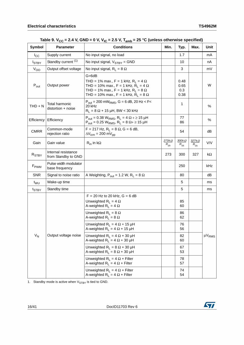
Table 9. VCC = 2.4 V, GND = 0 V, VIC = 2.5 V, Tamb = 25 °C (unless otherwise specified)
Symbol Parameter Conditions Min. Typ. Max. Unit
ICC Supply current No input signal, no load 1.7 mA
ISTBY Standby current (1) No input signal, VSTBY = GND 10 nA
VOO Output offset voltage No input signal, RL = 8 Ω 3 mV
Pout Output power
G=6dBTHD = 1% max., F = 1 kHz, RL = 4 Ω THD = 10% max., F = 1 kHz, RL = 4 Ω THD = 1% max., F = 1 kHz, RL = 8 Ω THD = 10% max., F = 1 kHz, RL = 8 Ω
0.480.650.30.38
W
THD + NTotal harmonic distortion + noise
Pout = 200 mWRMS, G = 6 dB, 20 Hz < F< 20 kHz RL = 8 Ω + 15 µH, BW < 30 kHz
1%
Efficiency EfficiencyPout = 0.38 WRMS, RL = 4 Ω + ≥ 15 µH Pout = 0.25 WRMS, RL = 8 Ω+ ≥ 15 µH
7786
%
CMRRCommon-mode rejection ratio
F = 217 Hz, RL = 8 Ω, G = 6 dB, ΔVicm = 200 mVpp
54 dB
Gain Gain value Rin in kΩ V/V
RSTBYInternal resistance from Standby to GND
273 300 327 kΩ
FPWM Pulse width modulator base frequency
250 kHz
SNR Signal to noise ratio A Weighting, Pout = 1.2 W, RL = 8 Ω 80 dB
tWU Wake-up time 5 ms
tSTBY Standby time 5 ms
VN Output voltage noise
F = 20 Hz to 20 kHz, G = 6 dB
Unweighted RL = 4 Ω A-weighted RL = 4 Ω
8560
μVRMS
Unweighted RL = 8 Ω A-weighted RL = 8 Ω
8662
Unweighted RL = 4 Ω + 15 µH A-weighted RL = 4 Ω + 15 µH
7656
Unweighted RL = 4 Ω + 30 µH A-weighted RL = 4 Ω + 30 µH
8260
Unweighted RL = 8 Ω + 30 µH A-weighted RL = 8 Ω + 30 µH
6753
Unweighted RL = 4 Ω + Filter A-weighted RL = 4 Ω + Filter
7857
Unweighted RL = 4 Ω + Filter A-weighted RL = 4 Ω + Filter
7454
1. Standby mode is active when VSTBY is tied to GND.
273kΩRin
------------------ 300kΩRin
------------------ 327kΩRin
------------------

DocID11703 Rev 6 17/41
TS4962M Electrical characteristic curves
41
5 Electrical characteristic curves
The graphs included in this section use the following abbreviations:
• RL + 15 μH or 30 μH = pure resistor + very low series resistance inductor
• Filter = LC output filter (1 µF+30 µH for 4 Ω and 0.5 µF+60 µH for 8 Ω)
• All measurements made with Cs1=1 µF and Cs2=100 nF except for PSRR where Cs1 is removed.
Figure 4. Test diagram for measurements
Figure 5. Test diagram for PSRR measurements
In+
In-
Rin
150k
Rin
150k
Cin
Cin
GND
Vcc
+Cs1
1uF
GND
Cs2
100nF
GND
RL
4 or 8 Ohms15uH or 30uH
or
LC Filter
5th order
50kHz low pass
filter
Audio Measurement
Bandwidth < 30kHz
Out+
Out-
TS4962
In+
In-
Rin
150k
Rin
150k
4.7uF
4.7uF
GND
Cs2
100nF
GND
RL
4 or 8 Ohms15uH or 30uH
or
LC Filter
5th order
50kHz low pass
filter
RMS Selective Measurement
Bandwidth=1% of Fmeas
Out+
Out-
TS4962
GND
5th order
50kHz low pass
filter
Reference
20Hz to 20kHz Vcc
GND

Electrical characteristic curves TS4962M
18/41 DocID11703 Rev 6
Figure 6. Current consumption vs. power supply voltage
Figure 7. Current consumption vs. standby voltage at VCC = 5 V
Figure 8. Current consumption vs. standby voltage at VCC = 3 V
Figure 9. Output offset voltage vs. common-mode input voltage
Figure 10. Efficiency vs. output power at VCC = 5 V and RL = 4 Ω
Figure 11. Efficiency vs. output power at VCC = 3 V and RL = 4 Ω

DocID11703 Rev 6 19/41
TS4962M Electrical characteristic curves
41
Figure 12. Efficiency vs. output power at VCC = 5 V and RL = 8 Ω
Figure 13. Efficiency vs. output power at VCC = 3 V and RL = 8 Ω
Figure 14. Output power vs. power supply voltage at RL = 4 Ω
Figure 15. Output power vs. power supply voltage at RL = 8 Ω
Figure 16. PSRR vs. frequency at RL = 4 Ω + 15 µH
Figure 17. PSRR vs. frequency at RL = 4 Ω + 30 µH

Electrical characteristic curves TS4962M
20/41 DocID11703 Rev 6
Figure 18. PSRR vs. frequency at RL = 4 Ω + filter
Figure 19. PSR R vs. frequency at RL = 8 Ω + 15 µH
Figure 20. PSRR vs. frequency at RL = 8 Ω + 30 µH
Figure 21. PSRR vs. frequency at RL = 8 Ω + filter
Figure 22. PSRR vs. common-mode input voltage
Figure 23. CMRR vs. frequency at RL = 4 Ω + 15 µH

DocID11703 Rev 6 21/41
TS4962M Electrical characteristic curves
41
Figure 24. CMRR vs. frequency at RL = 4 Ω + 30 µH
Figure 25. CMRR vs. frequency at RL = 4 Ω + filter
Figure 26. CMRR vs. frequency at RL = 8 Ω + 15 µH
Figure 27. CMRR vs. frequency at RL = 8 Ω + 30 µH
Figure 28. CMRR vs. frequency at RL = 8 Ω + filter
Figure 29. CMRR vs. common-mode input voltage

Electrical characteristic curves TS4962M
22/41 DocID11703 Rev 6
Figure 30. THD+N vs. output power at RL = 4 Ω + 15 µH, F = 100 Hz
Figure 31. THD+N vs. output power at RL = 4 Ω + 30 µH or filter, F = 100 Hz
Figure 32. THD+N vs. output power at RL = 8 Ω + 15 µH, F = 100 Hz
Figure 33. THD+N vs. output power at RL = 8 Ω + 30 µH or filter, F = 100 Hz
Figure 34. THD+N vs. output power at RL = 4 Ω + 15 µH, F = 1 kHz
Figure 35. THD+N vs. output power at RL = 4 Ω + 30 µH or filter, F = 1 kHz

DocID11703 Rev 6 23/41
TS4962M Electrical characteristic curves
41
Figure 36. THD+N vs. output power at RL = 8 Ω + 15 µH, F = 1 kHz
Figure 37. THD+N vs. output power at RL = 8 Ω + 30 µH or filter, F = 1 kHz
Figure 38. THD+N vs. frequency at RL = 4 Ω + 15 µH, VCC = 5 V
Figure 39. THD+N vs. frequency at RL = 4 Ω + 30 µH or filter, VCC = 5 V
Figure 40. THD+N vs. frequency at RL = 4 Ω + 15 µH, VCC = 3.6 V
Figure 41. THD+N vs. frequency at RL = 4 Ω + 30 H or filter, VCC = 3.6 V

Electrical characteristic curves TS4962M
24/41 DocID11703 Rev 6
Figure 42. THD+N vs. frequency at RL = 4 Ω + 15 µH, VCC = 2.5 V
Figure 43. THD+N vs. frequency at RL = 4 Ω + 30 µH or filter, VCC = 2.5 V
Figure 44. THD+N vs. frequency at RL = 8 Ω + 15 µH, VCC = 5 V
Figure 45. THD+N vs. frequency at RL = 8 Ω + 30 µH or filter, VCC = 5 V
Figure 46. THD+N vs. frequency at RL = 8 Ω + 15 µH, VCC = 3.6 V
Figure 47. THD+N vs. frequency at RL = 8 Ω + 30 µH or filter, VCC = 3.6 V

DocID11703 Rev 6 25/41
TS4962M Electrical characteristic curves
41
Figure 48. THD+N vs. frequency at RL = 8 Ω + 15 µH, VCC = 2.5 V
Figure 49. THD+N vs. frequency at RL = 8 Ω + 30 µH or filter, VCC = 2.5 V
Figure 50. Gain vs. frequency at RL = 4 Ω + 15 µH
Figure 51. Gain vs. frequency at RL = 4 Ω + 30 µH
Figure 52. Gain vs. frequency at RL = 4 Ω + filter
Figure 53. Gain vs. frequency at RL = 8 Ω + 15 µH
Electrical characteristic curves TS4962M
26/41 DocID11703 Rev 6
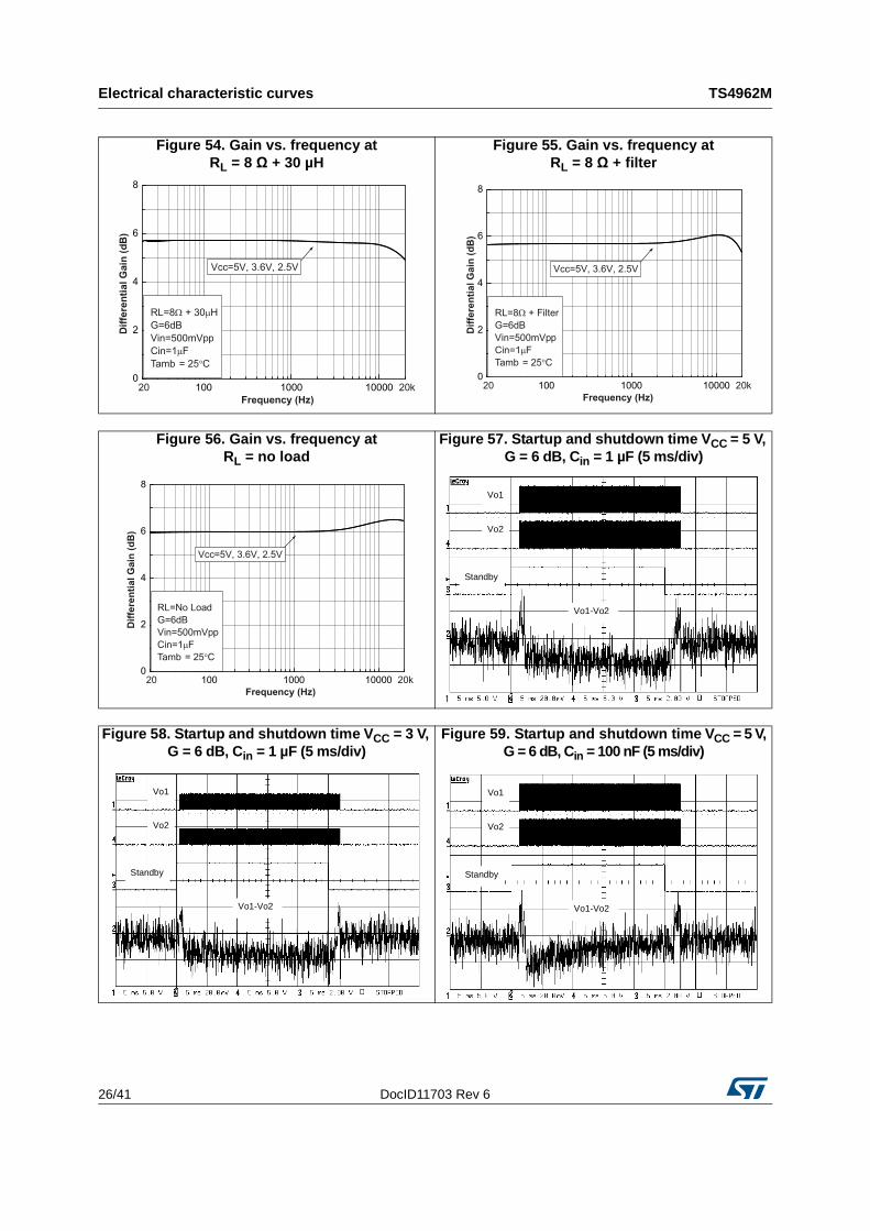
Figure 54. Gain vs. frequency at RL = 8 Ω + 30 µH
Figure 55. Gain vs. frequency at RL = 8 Ω + filter
Figure 56. Gain vs. frequency at RL = no load
Figure 57. Startup and shutdown time VCC = 5 V, G = 6 dB, Cin = 1 µF (5 ms/div)
Vo1
Vo2
Vo1-Vo2
Standby
Figure 58. Startup and shutdown time VCC = 3 V, G = 6 dB, Cin = 1 µF (5 ms/div)
Figure 59. Startup and shutdown time VCC = 5 V, G = 6 dB, Cin = 100 nF (5 ms/div)
Vo1
Vo2
Vo1-Vo2
Standby
Vo1
Vo2
Vo1-Vo2
Standby
DocID11703 Rev 6 27/41
TS4962M Electrical characteristic curves
41
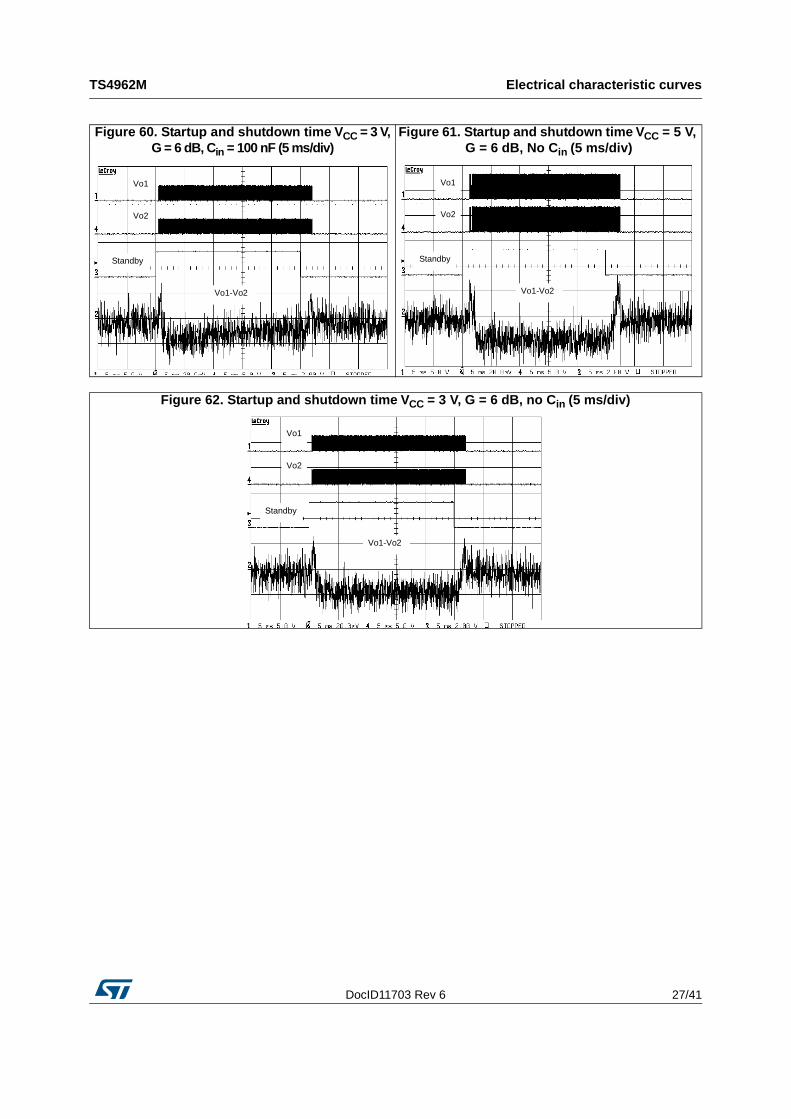
Figure 60. Startup and shutdown time VCC = 3 V, G = 6 dB, Cin = 100 nF (5 ms/div)
Figure 61. Startup and shutdown time VCC = 5 V, G = 6 dB, No Cin (5 ms/div)
Vo1
Vo2
Vo1-Vo2
Standby
Vo1
Vo2
Vo1-Vo2
Standby
Figure 62. Startup and shutdown time VCC = 3 V, G = 6 dB, no Cin (5 ms/div)
Vo1
Vo2
Vo1-Vo2
Standby

Application information TS4962M
28/41 DocID11703 Rev 6
6 Application information
6.1 Differential configuration principleThe TS4962M is a monolithic fully-differential input/output class D power amplifier. The TS4962M also includes a common-mode feedback loop that controls the output bias value to average it at VCC/2 for any DC common-mode input voltage. This allows the device to always have a maximum output voltage swing, and by consequence, maximizes the output power. Moreover, as the load is connected differentially compared to a single-ended topology, the output is four times higher for the same power supply voltage.
The advantages of a full-differential amplifier are:
• High PSRR (power supply rejection ratio)
• High common-mode noise rejection
• Virtually zero pop without additional circuitry, giving a faster start-up time compared to conventional single-ended input amplifiers.
• Easier interfacing with differential output audio DAC
• No input coupling capacitors required due to common-mode feedback loop
The main disadvantage is:
• As the differential function is directly linked to external resistor mismatching, particular attention to this mismatching is mandatory to obtain the best performance from the amplifier.
6.2 Gain in typical application schematicTypical differential applications are shown in Figure 3 on page 4.
In the flat region of the frequency-response curve (no input coupling capacitor effect), the differential gain is expressed by the relation:
with Rin expressed in kΩ.
Due to the tolerance of the internal 150 kΩ feedback resistor, the differential gain will be in the range (no tolerance on Rin):
AVdiff
Out+ Out-–
In+ In-–
-------------------------------300Rin----------= =
273Rin---------- AVdiff
327Rin----------≤ ≤

DocID11703 Rev 6 29/41
TS4962M Application information
41
6.3 Common-mode feedback loop limitationsThe common-mode feedback loop allows the output DC bias voltage to be averaged at VCC/2 for any DC common-mode bias input voltage.
However, due to Vicm limitation in the input stage (see Table 3: Operating conditions on page 5), the common-mode feedback loop can ensure its role only within a defined range. This range depends upon the values of VCC and Rin (AVdiff). To have a good estimation of the Vicm value, we can apply this formula (no tolerance on Rin):
with
and the result of the calculation must be in the range:
Due to the ±9% tolerance on the 150kΩ resistor, it is also important to check Vicm in these conditions:
If the result of the Vicm calculation is not in the previous range, input coupling capacitors must be used (with VCC from 2.4V to 2.5V, input coupling capacitors are mandatory).
Example
With VCC = 3 V, Rin = 150 k and VIC = 2.5 V, we typically find Vicm = 2 V and this is lower than 3V - 0.8 V = 2.2 V. With 136.5 kΩ we find 1.97 V, and with 163.5 kΩ we have 2.02 V. So, no input coupling capacitors are required.
6.4 Low frequency responseIf a low frequency bandwidth limitation is requested, it is possible to use input coupling capacitors.
In the low frequency region, Cin (input coupling capacitor) starts to have an effect. Cin forms, with Rin, a first order high-pass filter with a -3dB cut-off frequency:
So, for a desired cut-off frequency we can calculate Cin,
with Rin in Ω and FCL in Hz.
Vicm
VCC Rin× 2 VIC× 150kΩ×+
2 Rin 150kΩ+( )×---------------------------------------------------------------------------- (V)=
VICIn+ In-
+2
--------------------- (V)=
0.5V Vicm VCC 0.8V–≤ ≤
VCC Rin× 2 VIC× 136.5kΩ×+
2 Rin 136.5kΩ+( )×--------------------------------------------------------------------------------- Vicm
VCC Rin× 2 VIC× 163.5kΩ×+
2 Rin 163.5kΩ+( )×---------------------------------------------------------------------------------≤ ≤
FCL1
2π Rin× Cin×------------------------------------ (Hz)=
Cin1
2π Rin× FCL×-------------------------------------- (F)=

Application information TS4962M
30/41 DocID11703 Rev 6
6.5 Decoupling of the circuitA power supply capacitor, referred to as CS, is needed to correctly bypass the TS4962M.
The TS4962M has a typical switching frequency at 250 kHz and an output fall and rise time about 5ns. Due to these very fast transients, careful decoupling is mandatory.
A 1 µF ceramic capacitor is enough, but it must be located very close to the TS4962M in order to avoid any extra parasitic inductance created by an overly long track wire. In relation with dI/dt, this parasitic inductance introduces an overvoltage that decreases the global efficiency and, if it is too high, may cause a breakdown of the device.
In addition, even if a ceramic capacitor has an adequate high-frequency ESR value, its current capability is also important. A 0603 size is a good compromise, particularly when a 4 Ω load is used.
Another important parameter is the rated voltage of the capacitor. A 1 µF/6.3 V capacitor used at 5 V, loses about 50% of its value. In fact, with a 5V power supply voltage, the decoupling value is about 0.5 µF instead of 1µF. As CS has particular influence on the THD+N in the medium-high frequency region, this capacitor variation becomes decisive. In addition, less decoupling means higher overshoots, which can be problematic if they reach the power supply AMR value (6 V).
6.6 Wake-up time (tWU)When the standby is released to set the device ON, there is a wait of about 5ms. The TS4962M has an internal digital delay that mutes the outputs and releases them after this time in order to avoid any pop noise.
6.7 Shutdown time (tSTBY)When the standby command is set, the time required to put the two output stages into high impedance and to put the internal circuitry in shutdown mode, is about 5 ms. This time is used to decrease the gain and avoid any pop noise during shutdown.
6.8 Consumption in shutdown modeBetween the shutdown pin and GND there is an internal 300 kΩ resistor. This resistor forces the TS4962M to be in standby mode when the standby input pin is left floating.
However, this resistor also introduces additional power consumption if the shutdown pin voltage is not 0 V.
For example, with a 0.4 V standby voltage pin, Table 3: Operating conditions on page 5, shows that you must add 0.4 V/300 kΩ = 1.3 µA in typical (0.4 V/273 kΩ = 1.46 µA in maximum) to the shutdown current specified in Table 4 on page 6.

DocID11703 Rev 6 31/41
TS4962M Application information
41
6.9 Single-ended input configurationIt is possible to use the TS4962M in a single-ended input configuration. However, input coupling capacitors are needed in this configuration. The schematic in Figure 63 shows a single-ended input typical application.
Figure 63. Single-ended input typical application
All formulas are identical except for the gain (with Rin in kΩ):
And, due to the internal resistor tolerance we have:
In the event that multiple single-ended inputs are summed, it is important that the impedance on both TS4962M inputs (In- and In+) are equal.
Figure 64. Typical application schematic with multiple single-ended inputs
Rin
Rin
Cs1u
GND
GND
Vcc
SPEAKER
In-
Stdby
In+
Out-
Out+
VccC2
C1
A1
A2
A3
B1 B2
B3
C3
GND
InternalBias
PWM
Output
Bridge
H
Oscillator
150k
150k
+
-
300k
TS4962
Cin
Cin
Ve
GND
GND
Standby
AV glesin
Ve
Out+ Out-–-------------------------------
300Rin----------= =
273Rin---------- AV glesin
327Rin----------≤ ≤
Rin1
Req
Cs1u
GND
GND
Vcc
SPEAKER
Cin1
Ceq
Ve1
GND
GND
Standby
RinkCink
Vek
GND
In-
Stdby
In+
Out-
Out+
VccC2
C1
A1
A2
A3
B1 B2
B3
C3
GND
InternalBias
PWM
Output
Bridge
H
Oscillator
150k
150k
+
-
300k
TS4962

Application information TS4962M
32/41 DocID11703 Rev 6
We have the following equations:
In general, for mixed situations (single-ended and differential inputs), it is best to use the same rule, that is, to equalize impedance on both TS4962M inputs.
6.10 Output filter considerationsThe TS4962M is designed to operate without an output filter. However, due to very sharp transients on the TS4962M output, EMI radiated emissions may cause some standard compliance issues.
These EMI standard compliance issues can appear if the distance between the TS4962M outputs and loudspeaker terminal is long (typically more than 50mm, or 100mm in both directions, to the speaker terminals). As the PCB layout and internal equipment device are different for each configuration, it is difficult to provide a one-size-fits-all solution.
However, to decrease the probability of EMI issues, there are several simple rules to follow:
• Reduce, as much as possible, the distance between the TS4962M output pins and the speaker terminals.
• Use ground planes for “shielding” sensitive wires
• Place, as close as possible to the TS4962M and in series with each output, a ferrite bead with a rated current at minimum 2A and impedance greater than 50Ω at frequencies above 30MHz. If, after testing, these ferrite beads are not necessary, replace them by a short-circuit. Murata BLM18EG221SN1 or BLM18EG121SN1 are possible examples of devices you can use.
• Allow enough of a footprint to place, if necessary, a capacitor to short perturbations to ground (see the schematics in Figure 65).
Figure 65. Method for shorting pertubations to ground
Out+
Out-
– Ve1300
Rin1-------------× … Vek
300Rink-------------× (V)+ +=
Ceq
k
Σj 1=
Cinj=
Cinj1
2 π Rinj F××× CLj
---------------------------------------------------- (F)=
Req1
1Rinj
----------j 1=
k
-------------------=
Ferrite chip bead
about 100pF
Gnd
From TS4962 outputTo speaker

DocID11703 Rev 6 33/41
TS4962M Application information
41
In the case where the distance between the TS4962M outputs and speaker terminals is high, it is possible to have low frequency EMI issues due to the fact that the typical operating frequency is 250kHz. In this configuration, we recommend using an output filter (as shown in Figure 3: Typical application schematics on page 4). It should be placed as close as possible to the device.
6.11 Different examples with summed inputs
Example 1: Dual differential inputs
Figure 66. Typical application schematic with dual differential inputs
With (Ri in kΩ):
R1
R1
Cs1u
GND
GND
Vcc
SPEAKER
Standby
R2
R2
E1+
E1-
E2-
E2+
In-
Stdby
In+
Out-
Out+
VccC2
C1
A1
A2
A3
B1 B2
B3
C3
GND
InternalBias
PWM
Output
Bridge
H
Oscillator
150k
150k
+
-
300k
TS4962
AV1
Out+ Out-–
E1+ E1
-–
-------------------------------300R1----------= =
AV2
Out+ Out-–
E2+ E2
-–
-------------------------------300R2----------= =
0.5V VCC R1× R2 300 VIC1 R2 VIC2+× R1×( )×+×
300 R1 R2+( ) 2 R1× R2×+×--------------------------------------------------------------------------------------------------------------------------- VCC 0.8V–≤ ≤
VIC1
E1+ E1
-+
2------------------------= and VIC2
E2+ E2
-+
2------------------------=
Application information TS4962M
34/41 DocID11703 Rev 6
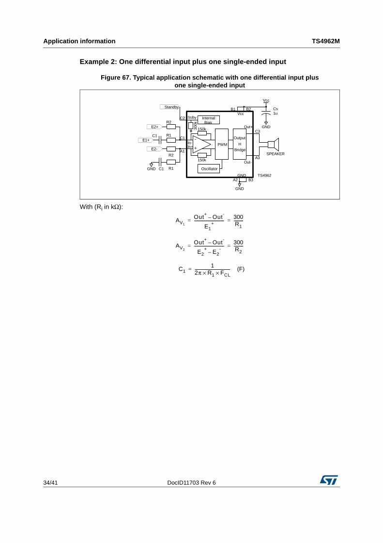
Example 2: One differential input plus one single-ended input
Figure 67. Typical application schematic with one differential input plus one single-ended input
With (Ri in kΩ):
R1
R2
Cs1u
GND
GND
Vcc
SPEAKER
Standby
R2
R1
E1+
E2-
E2+
In-
Stdby
In+
Out-
Out+
VccC2
C1
A1
A2
A3
B1 B2
B3
C3
GND
InternalBias
PWM
Output
Bridge
H
Oscillator
150k
150k
+
-
300k
TS4962
C1
C1GND
AV1
Out+ Out-–
E1+
-------------------------------300R1----------= =
AV2
Out+ Out-–
E2+ E2
-–
-------------------------------300R2----------= =
C11
2π R1× FCL×------------------------------------ (F)=

DocID11703 Rev 6 35/41
TS4962M Evaluation board
41
7 Evaluation board
An evaluation board for the TS4962M is available with a Flip Chip to DIP adapter. For more information about this board, refer to AN2134.
Figure 68. Schematic diagram of mono class D evaluation board for TS4962M
Figure 69. Diagram for Flip Chip to DIP adapter
In-
Stdby
In+
Out-
Out+
Vcc4
5
1
2
10
3 8
3
6
GND
InternalBias
PWM
Output
Bridge
H
Oscillator
150k
150k
+
-
300k
U1
TS4962 Flip-Chip to DIP Adapter
GND
Vcc
R1
150k
R2
150k
C2
100nF
C3
100nF
Cn3 Cn6
Cn2123
Cn1 + J1
GND GND
Vcc Vcc
+
C12.2uF/10V
GND
Cn4 + J2
Cn5 + J3
Positive Output
Negative Output
Positive Input
Negative input
In-
Stdby
In+
Out-
Out+
VccC2
C1
A1
A2
A3
B1 B2
B3
C3
GND
InternalBias
PWM
Output
Bridge
H
Oscillator
150k
150k
+
-
300k
TS4962
R1
OR
R2
OR
C1
100nF
+
C21uF
Pin4
Pin5
Pin1
Pin6
Pin10
Pin
3
pin8
Pin
2
Pin
9
Evaluation board TS4962M
36/41 DocID11703 Rev 6
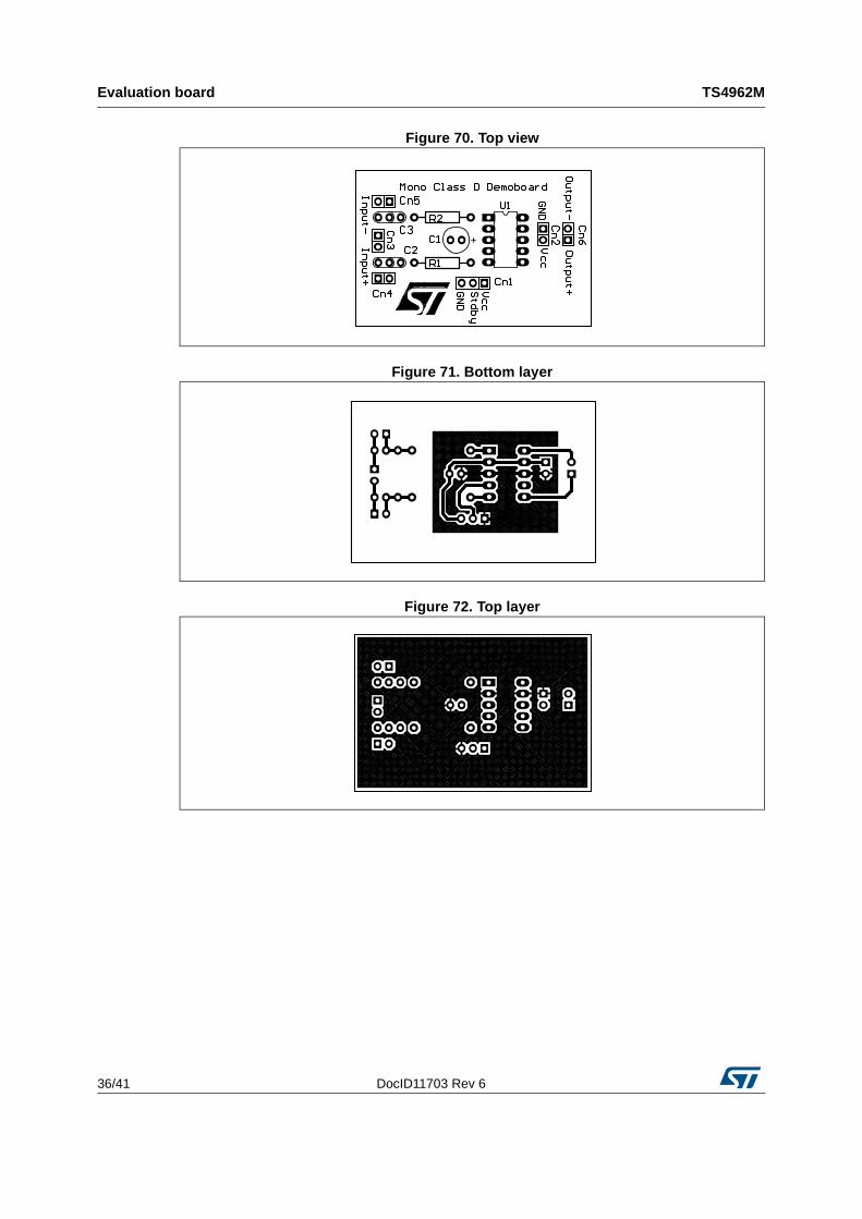
Figure 70. Top view
Figure 71. Bottom layer
Figure 72. Top layer

DocID11703 Rev 6 37/41
TS4962M Package information
41
8 Package information
In order to meet environmental requirements, ST offers these devices in different grades of ECOPACK® packages, depending on their level of environmental compliance. ECOPACK® specifications, grade definitions and product status are available at: www.st.com. ECOPACK® is an ST trademark.
8.1 9-bump Flip Chip package information
Figure 73. 9-bump Flip Chip package outline
Table 10. 9-bump Flip Chip mechanical data
Parameter Dimensions
Die size 1.6 mm x 1.6 mm ±30 µm
Die height (including bumps) 600 µm
Bump diameter 315 µm ±50 µm
Bump diameter before re-flow 300 µm ±10 µm
Bump height 250 µm ±40 µm
Die height 350 µm ±20 µm
Pitch 500 µm ±50 µm
Coplanarity 50 µm max.
Backside coating (optional, only for the TS4962MEIKJT)
25 µm ±3 µm

Package information TS4962M
38/41 DocID11703 Rev 6
Figure 74. 9-bump Flip Chip marking (top view)
1. Legend: ST logo E = symbol for lead-free First two “XX” = product code = 62 Third X = assembly code Three-digit date code, Y = year, WW = week Black dot is for marking pin A1
Figure 75. 9-bump Flip Chip recommended footprint
XXX
YWW
E
XXX
YWW
E
Pad in Cu 18μm with Flash NiAu (2-6μm, 0.2μm max.)
150μm min.
500μm
500μ
m
500μm
500μ
m
Φ=250μm
Φ=400μm typ.
75µm min.100μm max.
Track
Non Solder mask opening
Φ=340μm min.
Pad in Cu 18μm with Flash NiAu (2-6μm, 0.2μm max.)
150μm min.
500μm
500μ
m
500μm
500μ
m
Φ=250μm
Φ=400μm typ.
75µm min.100μm max.
Track
Non Solder mask opening
Φ=340μm min.
DocID11703 Rev 6 39/41
TS4962M Ordering information
41
9 Ordering information
Table 11. Order code table
Part number Temperature range Package Packing Marking
TS4962MEIJT
-40 °C to 85 °C
Lead-free Flip Chip
Tape and reel 62LTS4962MEIKJT
Lead-free Flip Chip with backside coating

Revision history TS4962M
40/41 DocID11703 Rev 6
10 Revision history
Table 12. Document revision history
Date Revision Changes
Oct. 2005 1First release corresponding to the product preview version.
Nov. 2005 2Electrical data updated for output voltage noise, see Table 4, Table 5, Table 6, Table 7, Table 8 and Table 9Formatting changes throughout.
Dec. 2005 3 Product in full production.
10-Jan-2007 4 Template update, no technical changes.
10-Oct-2016 5
Updated datasheet layout
Added package silhouettesAdded Related productsUpdated Applications
Section 5: Electrical characteristic curves: updated titles of graphs which had same titles.
Figure 73: 9-bump Flip Chip package outline: updated diagram to display the optional backside coating for order code TS4962MEIKJT.Added Table 10 to display package mechanical data as a separate table (with information concerning the optional backside coating for order code TS4962MEIKJT).Table 11: Order code table: updated marking of order code TS4962MEIJT, added order code TS4962MEIKJT.
15-Jan-2018 6 Updated Table 10: 9-bump Flip Chip mechanical data.

DocID11703 Rev 6 41/41
TS4962M
41
IMPORTANT NOTICE – PLEASE READ CAREFULLY
STMicroelectronics NV and its subsidiaries (“ST”) reserve the right to make changes, corrections, enhancements, modifications, and improvements to ST products and/or to this document at any time without notice. Purchasers should obtain the latest relevant information on ST products before placing orders. ST products are sold pursuant to ST’s terms and conditions of sale in place at the time of order acknowledgement.
Purchasers are solely responsible for the choice, selection, and use of ST products and ST assumes no liability for application assistance or the design of Purchasers’ products.
No license, express or implied, to any intellectual property right is granted by ST herein.
Resale of ST products with provisions different from the information set forth herein shall void any warranty granted by ST for such product.
ST and the ST logo are trademarks of ST. All other product or service names are the property of their respective owners.
Information in this document supersedes and replaces information previously supplied in any prior versions of this document.
© 2018 STMicroelectronics – All rights reserved

![Audio Filter Design - Aalto · Lecture #3: Audio Filter Design • Radians – Sampling frequency = 2π Axis [0, π] • Normalized – Sampling frequency = 1 Axis [0, 0.5] – Easy](https://img.pdfslide.us/doc/110x75/5fa0eeefa01d986b6b62ff99/audio-filter-design-aalto-lecture-3-audio-filter-design-a-radians-a-sampling.jpg)