Embed Size (px)
Citation preview

3300pFCSS
VIN
4x 22 FµCOUT
10 FµCIN
52.3kR1
10.0kR2
VOUT4
EN1
VIN2
GND3
PG7
SS/TR8
FB6
VOUT5
PAD9
U1
TPS82130
VOUT
Copyright © 2017, Texas Instruments Incorporated
1TIDUD32–June 2017Submit Documentation Feedback
Copyright © 2017, Texas Instruments Incorporated
3- to 11.5-VIN, –5-VOUT, 1.5-A Inverting Power Module Reference Design forSmall, Low-Noise Systems
TI Designs: TIDA-014573- to 11.5-VIN, –5-VOUT, 1.5-A Inverting Power ModuleReference Design for Small, Low-Noise Systems
DescriptionThis small and simple, low-noise inverting powermodule design (voltage inverter) cleanly supports a–5-V output voltage at up to 1.5 A of current from a3- to 11.5-V input. Featuring TI’s TPS82130MicroSiP™ power module step-down converter in aninverting buck-boost topology, the design achieves apower density of 584 mW/mm3 and a solution size ofless than 50 mm2, allowing it to power sensitive analogloads in space-constrained, high-temperaturecommunications equipment, such as optical modules.This design also supports many common industrialequipment, including those that require a 5-V input and–5-V output voltage inverter at up to 1 A.
Resources
TIDA-01457 Design FolderTPS82130 Product Folder
ASK Our E2E Experts
Features• Simple Power Module Design• Total Solution Size Less Than 50 mm2
• High Output Current of 1.5 A (VIN ≥ 7.5 V)• Wide Input Voltage Range of 3 to 11.5 V• Low Noise (Less Than 10-mV Output Ripple)• 125°C Rated Solution
Applications• Optical Line Card• Optical Modules• Optical Networking: EPON• Telecom Infrastructure: Remote Radio Unit (RRU)• General Purpose Industrial
An IMPORTANT NOTICE at the end of this TI reference design addresses authorized use, intellectual property matters and otherimportant disclaimers and information.

System Description www.ti.com
2 TIDUD32–June 2017Submit Documentation Feedback
Copyright © 2017, Texas Instruments Incorporated
3- to 11.5-VIN, –5-VOUT, 1.5-A Inverting Power Module Reference Design forSmall, Low-Noise Systems
1 System DescriptionA negative voltage around –5 V is frequently required to bias the laser driver in an optical module andother communications equipment. This function requires several hundred milliamps of current and ispowered from a 3.3-V source. This TI Design delivers an output current up to 600 mA at the lowest 3-Vinput voltage, which is a good match to the required output power and input voltage.
A negative voltage is also required in numerous industrial applications to bias operational amplifiers (opamps), programmable gain amplifiers (PGAs), and data converters (ADCs or DACs). In both applications,an integrated power module shortens the design time and enables a very-small solution size, while thelow-output noise has a minimal effect on the actual signal.
1.1 Key System Specifications
Table 1. Key System Specifications
PARAMETER SPECIFICATIONS DETAILSInput voltage range (VIN) 3 to 11.5 V —Output voltage (VOUT) –5 V —Output current (VIN ≥ 7.5 V) 1.5 A Figure 8Output current (VIN = 5 V) 1 A Figure 8Output current (VIN = 3 V) 600 mA Figure 8

VIN
CSS
COUT
CIN R1
R2
VOUT4
EN1
VIN2
GND3
PG7
SS/TR8
FB6
VOUT5
PAD9
U1
TPS82130
VOUT
Copyright © 2017, Texas Instruments Incorporated
3300pFCSS
VIN
4x 22 FµCOUT
10 FµCIN
52.3kR1
10.0kR2
VOUT4
EN1
VIN2
GND3
PG7
SS/TR8
FB6
VOUT5
PAD9
U1
TPS82130
VOUT
Copyright © 2017, Texas Instruments Incorporated
www.ti.com System Overview
3TIDUD32–June 2017Submit Documentation Feedback
Copyright © 2017, Texas Instruments Incorporated
3- to 11.5-VIN, –5-VOUT, 1.5-A Inverting Power Module Reference Design forSmall, Low-Noise Systems
2 System Overview
2.1 Block Diagram
Figure 1. TIDA-01457 Block Diagram
2.2 Highlighted Products
2.2.1 TPS82130The TPS82130 is a 3-A, step-down converter power module, which integrates the power inductor toachieve a very-small solution size and simple design. The power module accepts up to a 17-V inputvoltage from its input pin to ground pin. This wide input voltage range is ideally suited for an invertingconverter, which, at a minimum, requires a voltage rating of the input voltage plus the output voltage.
2.3 Design Considerations
2.3.1 Inverting Buck-Boost Topology ConceptThe inverting buck-boost topology is very similar to the buck topology. In the buck configuration thatFigure 2 shows, the positive connection (VOUT) is connected to the VOUT pin of the power module and thereturn connection is connected to the ground (GND) of the power module. However, in the inverting buck-boost configuration that Figure 3 shows, the power module ground is used as the negative output voltagepin (labeled as –VOUT). The terminal formerly known as the positive output in the buck configuration isused as the ground. This inverting topology allows the output voltage to be inverted and always lower thanthe ground.
Figure 2. TPS82130 Buck Topology

D =V
(V V )OUT
OUT IN-
I =L(Avg)
I
(1 D)OUT
-
(a) (b) (c)
+VIN
VO Load
iLVSW
–
Q1Control
Q2Sync
+
–
+VIN
VO Load
iLVSW
–
Q1Control
Q2Sync
+
–
+VIN
VO Load
iLVSW
–Q1
Control
Q2Sync
+
–
VIN
CSS
COUT
CIN R1
R2
-VOUT
VOUT4
EN1
VIN2
GND3
PG7
SS/TR8
FB6
VOUT5
PAD9
U1
TPS82130
Copyright © 2017, Texas Instruments Incorporated
System Overview www.ti.com
4 TIDUD32–June 2017Submit Documentation Feedback
Copyright © 2017, Texas Instruments Incorporated
3- to 11.5-VIN, –5-VOUT, 1.5-A Inverting Power Module Reference Design forSmall, Low-Noise Systems
Figure 3. TPS82130 Inverting Buck-Boost Topology
The circuit operation is different in the inverting buck-boost topology than in the buck topology. Figure 4ashows that the output voltage terminals are reversed, though the components are wired the same as abuck converter. As Figure 4b shows, during the ON-time of the control MOSFET, the inductor is chargedwith current while the output capacitor supplies the load current. The inductor does not provide current tothe load during this time. During the OFF-time of the control MOSFET and the ON-time of thesynchronous MOSFET (see Figure 4c), the inductor provides current to the load and the output capacitor.These changes affect many parameters, which the following subsections describe in further detail.
Figure 4. Inverting Buck-Boost Configuration
The average inductor current is affected in this topology. In the buck configuration, the average inductorcurrent is equal to the average output current because the inductor always supplies current to the loadduring both the ON- and OFF-times of the control MOSFET. However, in the inverting buck-boostconfiguration, only the output capacitor supplies the load with current, while the load is completelydisconnected from the inductor during the ON-time of the control MOSFET. During the OFF-time, theinductor connects to both the output capacitor and the load (see Figure 4). Because the OFF-time is 1 – Dof the switching period, the average inductor current in Equation 1 is calculated as:
(1)
The duty cycle for the typical buck converter is simply VOUT / VIN, but the calculation of the duty cycle inEquation 2 for an inverting buck-boost converter becomes:
(2)

LL L(avg)
II I
2
D= +
INL
S
V DI
f LD =
www.ti.com System Overview
5TIDUD32–June 2017Submit Documentation Feedback
Copyright © 2017, Texas Instruments Incorporated
3- to 11.5-VIN, –5-VOUT, 1.5-A Inverting Power Module Reference Design forSmall, Low-Noise Systems
Equation 3 provides the peak-to-peak inductor ripple current:
(3)
where:• ΔIL (A): Peak-to-peak inductor ripple current• D: Duty cycle• fS (MHz): Switching frequency• L (µH): Inductor value of typically 1 µH• VIN (V): Input voltage with respect to ground, not with respect to the device ground or VOUT
Equation 4 calculates the maximum inductor current:
(4)
2.3.2 VIN and VOUT RangeThe input voltage that can be applied to an integrated circuit (IC) operating in the inverting buck-boosttopology is less than the input voltage for the same IC operating in the buck topology. The reason for thisdifference is because the ground pin of the IC is connected to the (negative) output voltage. Therefore, theinput voltage across the device is VIN to VOUT, not VIN to ground. Thus, the input voltage range of theTPS82130 is 3 to 17 V + VOUT, where VOUT is a negative value.
The output voltage range is the same as when configured as a buck converter, but negative. The outputvoltage for the inverting buck-boost topology must be set between –0.9 and –6 V. The output voltage isset in the same way as the buck configuration, with two resistors connected to the FB pin. Use the sameequation in the TPS82130 datasheet to set the output voltage, keeping both VOUT and VFB as positivevalues. The TIDA-01457 design sets the output voltage at –5 V, which gives an input voltage range of 3 to12 V. However, it is not recommended to use a 12-V input voltage because voltage tolerances on theinput supply can violate the recommended operating range of the TPS82130.
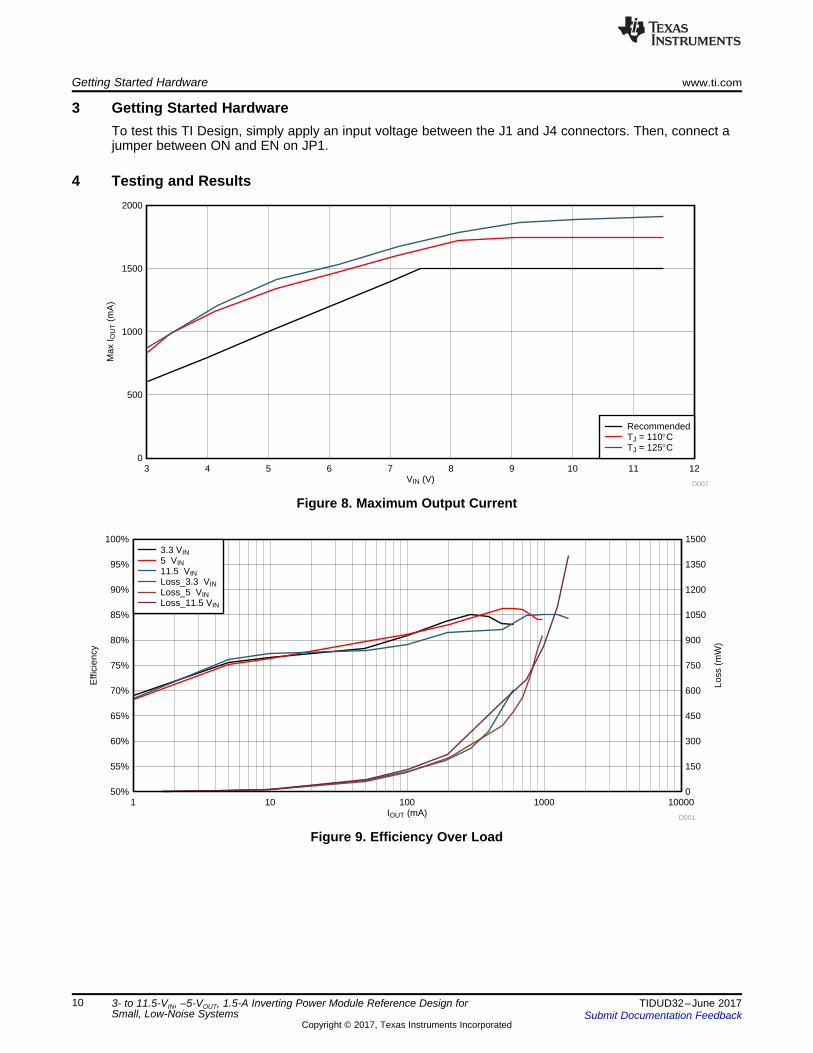
2.3.3 Maximum Output CurrentIn the inverting buck-boost topology, the maximum output current is reduced as compared to the bucktopology. This reduction is a result of the peak inductor current being higher, as calculated in Equation 4.With a power module, there are additional thermal limits arising from the small size of the power moduleitself. Finally, there are further limits on the maximum output current that occur from stability due to theright-half plane zero, which occurs in the inverting buck-boost topology. Figure 8 shows the maximumoutput current based on temperature rise and stability for the TIDA-01457 design. The current limit for theTPS82130 device occurs above all curves in Figure 8 and therefore does not limit the maximum outputcurrent more than thermal or stability limits. The current limit itself still operates to limit the peak inductorcurrent.
2.3.3.1 Thermal LimitsThe primary maximum output current limitation in most designs is a thermal limitation. As the outputcurrent increases, the absolute power loss (in mW) in the TPS82130 also increases, which causes ahigher temperature rise across the thermal impedance of the TPS82130 device.
The TPS82130 datasheet recommends operating below a device temperature of 110°C and forbidsoperating above 125°C for reliability. Therefore, Figure 8 contains two thermal limit lines: one for a 110°Cand one for a 125°C operating temperature. These lines are calculated by multiplying the power loss ofthe TPS82130 from Figure 9 by the θJA of the TPS82130EVM-720, which is provided in the devicedatasheet as 46.1°C/W, and adding this value to a 25°C ambient temperature.

- - ´
=
´ ´ ´ ´ p
2OUT
(RHP)OUT
(1 D) Vf
(D L I 2 )
JA
A _MAXLOSS
125 TP
-
q£
System Overview www.ti.com
6 TIDUD32–June 2017Submit Documentation Feedback
Copyright © 2017, Texas Instruments Incorporated
3- to 11.5-VIN, –5-VOUT, 1.5-A Inverting Power Module Reference Design forSmall, Low-Noise Systems
Using this method, the maximum output current at any ambient temperature can be calculated. Simplysubtract the maximum ambient temperature from either 110°C or 125°C to obtain the allowabletemperature rise. Divide the θJA of the printed circuit board (PCB) by this temperature rise to obtain theallowable power loss. Find this power loss in Figure 9 to determine the maximum output current underspecific conditions. 46.1°C/W is useful as an estimate of θJA. See Equation 5 for the calculation.
(5)
2.3.3.2 Stability Limits and Output Capacitor SelectionThe "recommended" curve in Figure 8 shows the recommended maximum output current based onstability. The TIDA-01457 design must be operated at load currents below this line. In most applications,which have ambient temperatures above 25°C, the thermal limit lines move down below the recommendedline (as explained in Section 2.3.3.1), which further limits the maximum output current.
The inverting buck-boost topology contains a right-half plane zero, which significantly and negativelyimpacts the control loop response by adding an increase in gain along with a decrease in phase at a highfrequency. This right-half plane zero can cause instability. Equation 6 estimates the frequency of the right-half plane zero.
(6)
The TIDA-01457 design uses four 22-µF output capacitors, which have an effective capacitance of about36 µF at the –5-V output voltage. This amount of capacitance pushes the crossover frequency of thecontrol loop down to frequencies low enough so that the right-half plane zero is sufficiently higher infrequency for stability. While one of these output capacitors requires placement near the TPS82130device, the others can be placed at the point of load and serve as their input decoupling capacitor. Whenthree of the output capacitors are placed at the point of load, the solution size is below 50 mm2. If thesethree capacitors are included, the solution size of all components shown within the "Active Circuitry" boxon the front page becomes around 75 mm2.
More output capacitance improves stability by increasing the separation between the right-half plane zeroand crossover. The right-half plane zero frequency occurs at lower frequencies with lower input voltages,which have a higher duty cycle. Load transient testing is the best test for stability, as described in theSimplifying Stability Checks application report (SLVA381) [1]. Because the VOS pin of the TPS82130 isconnected on the device, it is impossible to break the entire control loop and measure a bode plot.
2.3.4 Enable Pin ConfigurationThe device is enabled when the voltage at the EN pin trips its threshold and the input voltage is above theundervoltage lockout (UVLO) threshold. The TPS82130 device stops operation when the voltage on theEN pin falls below its threshold or the input voltage falls below the UVLO threshold.
Because VOUT is the IC ground in this configuration, the EN pin must be referenced to VOUT instead ofground. In the buck configuration, 0.9 V is considered as high and less than 0.3 V is considered as low. Inthe inverting buck-boost configuration, however, the VOUT voltage is the reference; therefore, the highthreshold is 0.9 V + VOUT and the low threshold is 0.3 V + VOUT. For example, if VOUT = –5 V, then VEN isconsidered at a high level for voltages above –4.1 V and a low level for voltages below –4.7 V.

1 MΩ 1 MΩ
VIN
SYS_EN
Q2PMOS
Q1NMOS
S
S
D
D
EN
–VOUT
G
G
www.ti.com System Overview
7TIDUD32–June 2017Submit Documentation Feedback
Copyright © 2017, Texas Instruments Incorporated
3- to 11.5-VIN, –5-VOUT, 1.5-A Inverting Power Module Reference Design forSmall, Low-Noise Systems
This behavior can cause difficulties enabling or disabling the part because, in some applications, the ICproviding the EN signal may not be able to produce negative voltages. The level-shifter circuit thatFigure 5 shows removes any difficulties associated with the offset EN threshold voltages by eliminatingthe requirement for negative EN signals. If disabling the TPS82130 is not desired, the EN pin may bedirectly connected to VIN without this circuit.
NOTE: VOUT is the negative output voltage of the inverting buck-boost converter
Figure 5. EN Pin Level Shifter
The positive signal that originally drove EN is instead tied to the gate of Q1 (SYS_EN). When Q1 is OFF(SYS_EN grounded), Q2 has 0 V across its VGS and also remains OFF. In this state, the EN pin is initiallyat the level of the output voltage (–5 V), which is below the low-level threshold, and disables the device.
When SYS_EN provides enough positive voltage to turn Q1 ON (VGS threshold as specified in theMOSFET datasheet), the gate of Q2 is at ground potential through Q1. This action drives the VGS of Q2negative and turns Q2 ON. Then VIN ties to EN through Q2 and the pin is above the high-level threshold,which turns the device ON. Be careful to ensure that the VGD and VGS of Q2 remain within the MOSFETratings during both the enabled and disabled states. Failing to adhere to this constraint can result indamaged MOSFETs.
Figure 24 and Figure 25 show the enable and disable sequence. The SYS_EN signal activates the enablecircuit and the G/D node signal represents the shared node between Q1 and Q2. This circuit has beentested with a 5-V SYS_EN signal and dual N/PFET Si1029X. The EN signal is the output of the circuit andgoes from VIN to VOUT to properly enable and disable the device. The PG pin is used as an outputdischarge to accelerate the return of VOUT to 0 V, when the IC is disabled.

S
S
S100k
VCC
–VOUT
–VOUT
Q3NMOS
Q1NMOS
Q2NMOS
PG
SYS_PG
G
G
G
D
D
D
Inside TPS82130
100k
100k
Copyright © 2017, Texas Instruments Incorporated
System Overview www.ti.com
8 TIDUD32–June 2017Submit Documentation Feedback
Copyright © 2017, Texas Instruments Incorporated
3- to 11.5-VIN, –5-VOUT, 1.5-A Inverting Power Module Reference Design forSmall, Low-Noise Systems
2.3.5 Power Good Pin ConfigurationThe TPS82130 has a built-in power good (PG) function to indicate whether the output voltage has reachedits appropriate level or not. The PG pin is an open-drain output that requires a pullup resistor. BecauseVOUT is the IC ground in this configuration, the PG pin is referenced to VOUT instead of ground, whichmeans that the TPS82130 device pulls PG to VOUT when it is low.
This behavior can cause difficulties in reading the state of the PG pin, because in some applications theIC detecting the voltage level of the PG pin may not be able to withstand negative voltages. The level-shifter circuit shown in Figure 6 removes any difficulties associated with the offset PG pin voltages byeliminating the negative output signals of the PG pin. If the PG pin functionality is not required, it may beleft floating or connected to VOUT without this circuit. Note that to avoid violating its absolute maximumrating, the PG pin should not be driven more than 6 V above the negative output voltage (IC ground).
Figure 6. PG Pin Level Shifter
Inside the TPS82130, the PG pin is connected to an N-channel MOSFET (Q3). By tying the PG pin to thegate of Q1, when the PG pin is pulled low, Q1 is off and Q2 is on because Q2's VGS is at VCC. SYS_PG isthen pulled to ground.
When Q3 turns OFF, the gate of Q1 is pulled to ground potential which turns Q1 ON. This sequence ofevents pulls the gate of Q2 below ground, which turns it OFF. SYS_PG is then pulled up to the VCCvoltage. Note that the VCC voltage must be at an appropriate logic level for the circuitry connected to theSYS_PG net.
Figure 26 and Figure 27 show this PG pin level-shifter sequence. The PG signal activates the PG pinlevel-shifter circuit and the G/D node signal represents the shared node between Q1 and Q2. This circuithas been tested with a VCC of 5 V and dual NFET Si1902DL. The SYS_PG net is the output of the circuitand goes between ground and 5 V and is easily read by a separate device.
VIN
CSS
COUT
CIN R1
R2
-VOUT
VOUT4
EN1
VIN2
GND3
PG7
SS/TR8
FB6
VOUT5
PAD9
U1
TPS82130
CBP
D1
Copyright © 2017, Texas Instruments Incorporated
www.ti.com System Overview
9TIDUD32–June 2017Submit Documentation Feedback
Copyright © 2017, Texas Instruments Incorporated
3- to 11.5-VIN, –5-VOUT, 1.5-A Inverting Power Module Reference Design forSmall, Low-Noise Systems
2.3.6 Discharging Output VoltageIf the TPS82130 device is disabled in a light-load or no-load condition, the PG pin can accelerate return ofVOUT to 0 V by providing an additional discharge path. When the IC has been disabled through the EN pin,the PG pin is connected to the device ground (–VOUT) through an internal MOSFET. Placing a resistorbetween ground and the PG pin creates a discharge path to ground.
The added resistor must be sized to limit the current into the PG pin to a safe level, which the TPS82130datasheet specifies as 10 mA at maximum. A 499-Ω PG resistor has been chosen for this –5-V outputvoltage.
2.3.7 Adjustable Soft-Start TimeThe TPS82130 features an adjustable soft-start time. The soft-start time is the rise time of the outputvoltage and is adjustable with the capacitor, CSS, on the SS/TR pin. If needed, the output voltage risetime is adjustable to match the rise time of a corresponding 5-V rail in the system. The soft-start time isset in the same way as described in the TPS82130 datasheet[3].
2.3.8 Input Capacitor SelectionAn input capacitor, CIN, is required to provide a local bypass for the input voltage source. A low equivalentseries resistance (ESR) X5R or X7R ceramic capacitor is best for input voltage filtering and minimizinginterference with other circuits. For most applications, a 10-µF ceramic capacitor is recommended from VINto ground (system ground, not –VOUT). The CIN capacitor value can be increased without any limit forbetter input voltage filtering.
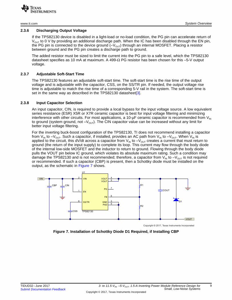
For the inverting buck-boost configuration of the TPS82130, TI does not recommend installing a capacitorfrom VIN to –VOUT. Such a capacitor, if installed, provides an AC path from VIN to –VOUT. When VIN isapplied to the circuit, this dV/dt across a capacitor from VIN to –VOUT creates a current that must return toground (the return of the input supply) to complete its loop. This current may flow through the body diodeof the internal low-side MOSFET and the inductor to return to ground. Flowing through the body diodepulls the VOUT pin below IC ground, which violates its absolute maximum rating. Such a condition maydamage the TPS82130 and is not recommended; therefore, a capacitor from VIN to –VOUT is not requiredor recommended. If such a capacitor (CBP) is present, then a Schottky diode must be installed on theoutput, as the schematic in Figure 7 shows.
Figure 7. Installation of Schottky Diode D1 Required, if Installing CBP
IOUT (mA)
Effi
cien
cy
Loss
(m
W)
1 10 100 1000 1000050% 0
55% 150
60% 300
65% 450
70% 600
75% 750
80% 900
85% 1050
90% 1200
95% 1350
100% 1500
D001
3.3 VIN5 VIN11.5 VINLoss_3.3 VINLoss_5 VINLoss_11.5 VIN
VIN (V)
Max
I OU
T (
mA
)
3 4 5 6 7 8 9 10 11 120
500
1000
1500
2000
D007
RecommendedTJ = 110qCTJ = 125qC
Getting Started Hardware www.ti.com
10 TIDUD32–June 2017Submit Documentation Feedback
Copyright © 2017, Texas Instruments Incorporated
3- to 11.5-VIN, –5-VOUT, 1.5-A Inverting Power Module Reference Design forSmall, Low-Noise Systems
3 Getting Started HardwareTo test this TI Design, simply apply an input voltage between the J1 and J4 connectors. Then, connect ajumper between ON and EN on JP1.
4 Testing and Results
Figure 8. Maximum Output Current
Figure 9. Efficiency Over Load

VIN (V)
Line
Reg
ulat
ion
3 5 7 9 11 13-1.00%
-0.75%
-0.50%
-0.25%
0.00
0.25%
0.50%
0.75%
1.00%
D004 VIN (V)
Sw
itchi
ng F
requ
ency
(M
Hz)
3 5 7 9 11 131.5
1.6
1.7
1.8
1.9
2
2.1
2.2
D005
IOUT (mA)
Load
Reg
ulat
ion
1 10 100 1000 5000-1.00%
-0.75%
-0.50%
-0.25%
0.00
0.25%
0.50%
0.75%
1.00%
D002
3.3 VIN5 VIN11.5 VIN
VIN (V)
Effi
cien
cy
3 5 7 9 11 1380%
81%
82%
83%
84%
85%
86%
87%
88%
89%
90%
D006
www.ti.com Testing and Results
11TIDUD32–June 2017Submit Documentation Feedback
Copyright © 2017, Texas Instruments Incorporated
3- to 11.5-VIN, –5-VOUT, 1.5-A Inverting Power Module Reference Design forSmall, Low-Noise Systems
Figure 10. Efficiency Over VIN (600-mA Load)
Figure 11. Load Regulation
Figure 12. Line Regulation (600-mA Load) Figure 13. Switching Frequency Over VIN (600-mA Load)
IOUT (mA)
Sw
itchi
ng F
requ
ency
(M
Hz)
1 10 100 1000 50000.001
0.01
0.1
1
10
D003
3.3 VIN5 VIN11.5 VIN
Testing and Results www.ti.com
12 TIDUD32–June 2017Submit Documentation Feedback
Copyright © 2017, Texas Instruments Incorporated
3- to 11.5-VIN, –5-VOUT, 1.5-A Inverting Power Module Reference Design forSmall, Low-Noise Systems
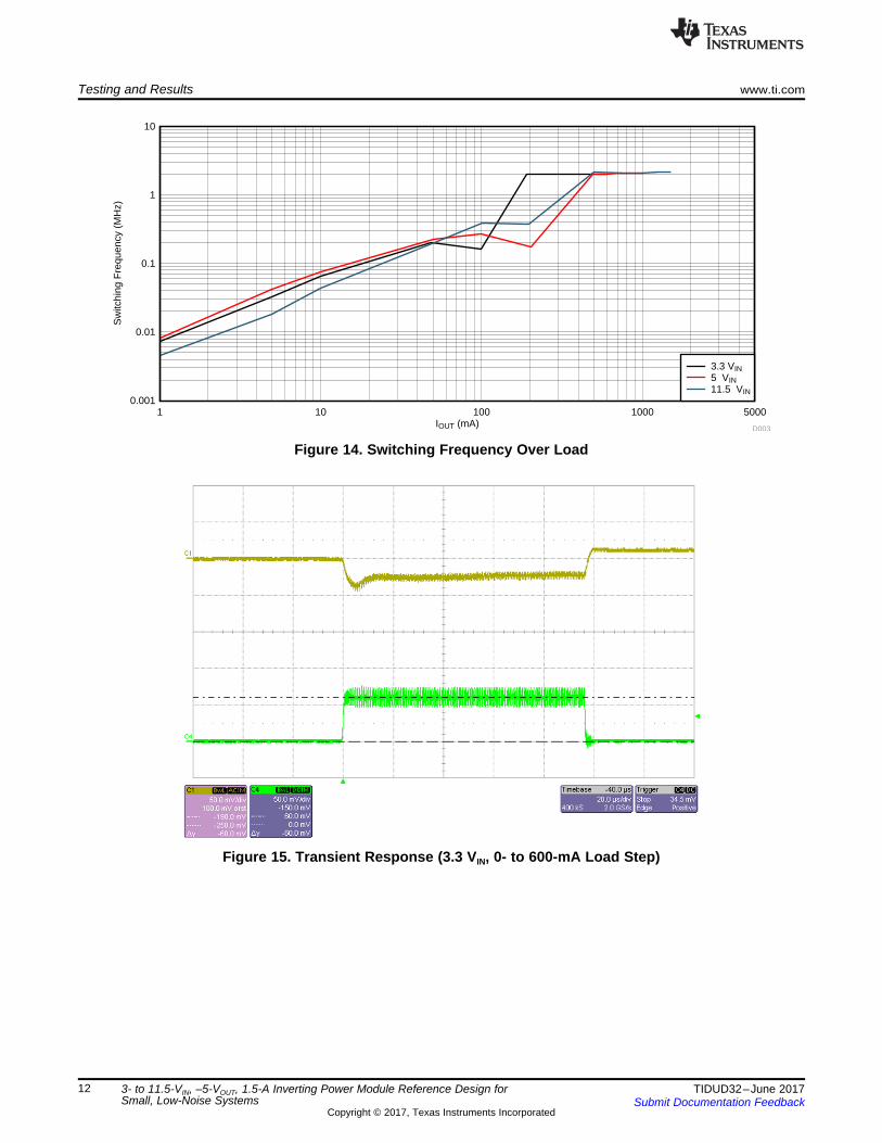
Figure 14. Switching Frequency Over Load
Figure 15. Transient Response (3.3 VIN, 0- to 600-mA Load Step)

www.ti.com Testing and Results
13TIDUD32–June 2017Submit Documentation Feedback
Copyright © 2017, Texas Instruments Incorporated
3- to 11.5-VIN, –5-VOUT, 1.5-A Inverting Power Module Reference Design forSmall, Low-Noise Systems
Figure 16. Transient Response (5 VIN, 0- to 1-A Load Step)
Figure 17. Transient Response (7.5 VIN, 0- to 1.5-A Load Step)

Testing and Results www.ti.com
14 TIDUD32–June 2017Submit Documentation Feedback
Copyright © 2017, Texas Instruments Incorporated
3- to 11.5-VIN, –5-VOUT, 1.5-A Inverting Power Module Reference Design forSmall, Low-Noise Systems
Figure 18. Output Voltage Ripple (3.3 VIN, 1-mA Load)
Figure 19. Output Voltage Ripple (3.3 VIN, 600-mA Load)

www.ti.com Testing and Results
15TIDUD32–June 2017Submit Documentation Feedback
Copyright © 2017, Texas Instruments Incorporated
3- to 11.5-VIN, –5-VOUT, 1.5-A Inverting Power Module Reference Design forSmall, Low-Noise Systems
Figure 20. Output Voltage Ripple (5 VIN, 1-mA Load)
Figure 21. Output Voltage Ripple (5 VIN, 1-A Load)

Testing and Results www.ti.com
16 TIDUD32–June 2017Submit Documentation Feedback
Copyright © 2017, Texas Instruments Incorporated
3- to 11.5-VIN, –5-VOUT, 1.5-A Inverting Power Module Reference Design forSmall, Low-Noise Systems
Figure 22. Output Voltage Ripple (11.5 VIN, 1-mA Load)
Figure 23. Output Voltage Ripple (11.5 VIN, 1.5-A Load)

SYS_EN
G/D Node
EN
VOUT
SYS_EN
G/D Node
EN
VOUT
www.ti.com Testing and Results
17TIDUD32–June 2017Submit Documentation Feedback
Copyright © 2017, Texas Instruments Incorporated
3- to 11.5-VIN, –5-VOUT, 1.5-A Inverting Power Module Reference Design forSmall, Low-Noise Systems
Figure 24. Start-up on EN (5 VIN, No Load)
Figure 25. Shutdown on EN (5 VIN, No Load)

SYS_PG
G/D Node
PG
VOUT
SYS_PG
G/D Node
PG
VOUT
Testing and Results www.ti.com
18 TIDUD32–June 2017Submit Documentation Feedback
Copyright © 2017, Texas Instruments Incorporated
3- to 11.5-VIN, –5-VOUT, 1.5-A Inverting Power Module Reference Design forSmall, Low-Noise Systems
Figure 26. PG on Start-up (5 VIN, No Load)
Figure 27. PG on Shutdown (5 VIN, No Load)

www.ti.com Design Files
19TIDUD32–June 2017Submit Documentation Feedback
Copyright © 2017, Texas Instruments Incorporated
3- to 11.5-VIN, –5-VOUT, 1.5-A Inverting Power Module Reference Design forSmall, Low-Noise Systems
5 Design Files
5.1 SchematicsTo download the schematics, see the design files at TIDA-01457.
5.2 Bill of MaterialsTo download the bill of materials (BOM), see the design files at TIDA-01457.
5.3 PCB Layout Recommendations
5.3.1 Layout PrintsTo download the layer plots, see the design files at TIDA-01457.
5.4 Gerber FilesTo download the Gerber files, see the design files at TIDA-01457.
5.5 Assembly DrawingsTo download the assembly drawings, see the design files at TIDA-01457.
6 Related Documentation
1. Texas Instruments, Simplifying Stability Checks, Application Report (SLVA381)2. Texas Instruments, Using the TPS62125 in an Inverting Buck-Boost Topology,
TPS62125 Application Report (SLVA514)3. Texas Instruments, TPS82130 17-V Input 3-A Step-Down Converter MicroSiP™ Module with
Integrated Inductor, TPS82130 Datasheet (SLVSCY5)
6.1 TrademarksMicroSiP is a trademark of Texas Instruments.All other trademarks are the property of their respective owners.

IMPORTANT NOTICE FOR TI DESIGN INFORMATION AND RESOURCES
Texas Instruments Incorporated (‘TI”) technical, application or other design advice, services or information, including, but not limited to,reference designs and materials relating to evaluation modules, (collectively, “TI Resources”) are intended to assist designers who aredeveloping applications that incorporate TI products; by downloading, accessing or using any particular TI Resource in any way, you(individually or, if you are acting on behalf of a company, your company) agree to use it solely for this purpose and subject to the terms ofthis Notice.TI’s provision of TI Resources does not expand or otherwise alter TI’s applicable published warranties or warranty disclaimers for TIproducts, and no additional obligations or liabilities arise from TI providing such TI Resources. TI reserves the right to make corrections,enhancements, improvements and other changes to its TI Resources.You understand and agree that you remain responsible for using your independent analysis, evaluation and judgment in designing yourapplications and that you have full and exclusive responsibility to assure the safety of your applications and compliance of your applications(and of all TI products used in or for your applications) with all applicable regulations, laws and other applicable requirements. Yourepresent that, with respect to your applications, you have all the necessary expertise to create and implement safeguards that (1)anticipate dangerous consequences of failures, (2) monitor failures and their consequences, and (3) lessen the likelihood of failures thatmight cause harm and take appropriate actions. You agree that prior to using or distributing any applications that include TI products, youwill thoroughly test such applications and the functionality of such TI products as used in such applications. TI has not conducted anytesting other than that specifically described in the published documentation for a particular TI Resource.You are authorized to use, copy and modify any individual TI Resource only in connection with the development of applications that includethe TI product(s) identified in such TI Resource. NO OTHER LICENSE, EXPRESS OR IMPLIED, BY ESTOPPEL OR OTHERWISE TOANY OTHER TI INTELLECTUAL PROPERTY RIGHT, AND NO LICENSE TO ANY TECHNOLOGY OR INTELLECTUAL PROPERTYRIGHT OF TI OR ANY THIRD PARTY IS GRANTED HEREIN, including but not limited to any patent right, copyright, mask work right, orother intellectual property right relating to any combination, machine, or process in which TI products or services are used. Informationregarding or referencing third-party products or services does not constitute a license to use such products or services, or a warranty orendorsement thereof. Use of TI Resources may require a license from a third party under the patents or other intellectual property of thethird party, or a license from TI under the patents or other intellectual property of TI.TI RESOURCES ARE PROVIDED “AS IS” AND WITH ALL FAULTS. TI DISCLAIMS ALL OTHER WARRANTIES ORREPRESENTATIONS, EXPRESS OR IMPLIED, REGARDING TI RESOURCES OR USE THEREOF, INCLUDING BUT NOT LIMITED TOACCURACY OR COMPLETENESS, TITLE, ANY EPIDEMIC FAILURE WARRANTY AND ANY IMPLIED WARRANTIES OFMERCHANTABILITY, FITNESS FOR A PARTICULAR PURPOSE, AND NON-INFRINGEMENT OF ANY THIRD PARTY INTELLECTUALPROPERTY RIGHTS.TI SHALL NOT BE LIABLE FOR AND SHALL NOT DEFEND OR INDEMNIFY YOU AGAINST ANY CLAIM, INCLUDING BUT NOTLIMITED TO ANY INFRINGEMENT CLAIM THAT RELATES TO OR IS BASED ON ANY COMBINATION OF PRODUCTS EVEN IFDESCRIBED IN TI RESOURCES OR OTHERWISE. IN NO EVENT SHALL TI BE LIABLE FOR ANY ACTUAL, DIRECT, SPECIAL,COLLATERAL, INDIRECT, PUNITIVE, INCIDENTAL, CONSEQUENTIAL OR EXEMPLARY DAMAGES IN CONNECTION WITH ORARISING OUT OF TI RESOURCES OR USE THEREOF, AND REGARDLESS OF WHETHER TI HAS BEEN ADVISED OF THEPOSSIBILITY OF SUCH DAMAGES.You agree to fully indemnify TI and its representatives against any damages, costs, losses, and/or liabilities arising out of your non-compliance with the terms and provisions of this Notice.This Notice applies to TI Resources. Additional terms apply to the use and purchase of certain types of materials, TI products and services.These include; without limitation, TI’s standard terms for semiconductor products http://www.ti.com/sc/docs/stdterms.htm), evaluationmodules, and samples (http://www.ti.com/sc/docs/sampterms.htm).
Mailing Address: Texas Instruments, Post Office Box 655303, Dallas, Texas 75265Copyright © 2017, Texas Instruments Incorporated