Embed Size (px)
Citation preview
1FEATURES
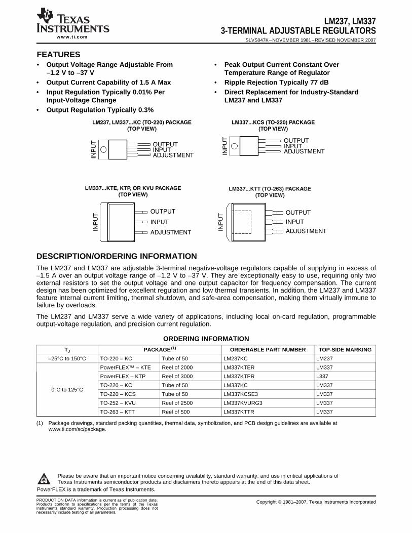
LM337...KTE, KTP, OR KVU PACKAGE
(TOP VIEW)
OUTPUT
INPUT
ADJUSTMENT
INP
UT
INP
UT
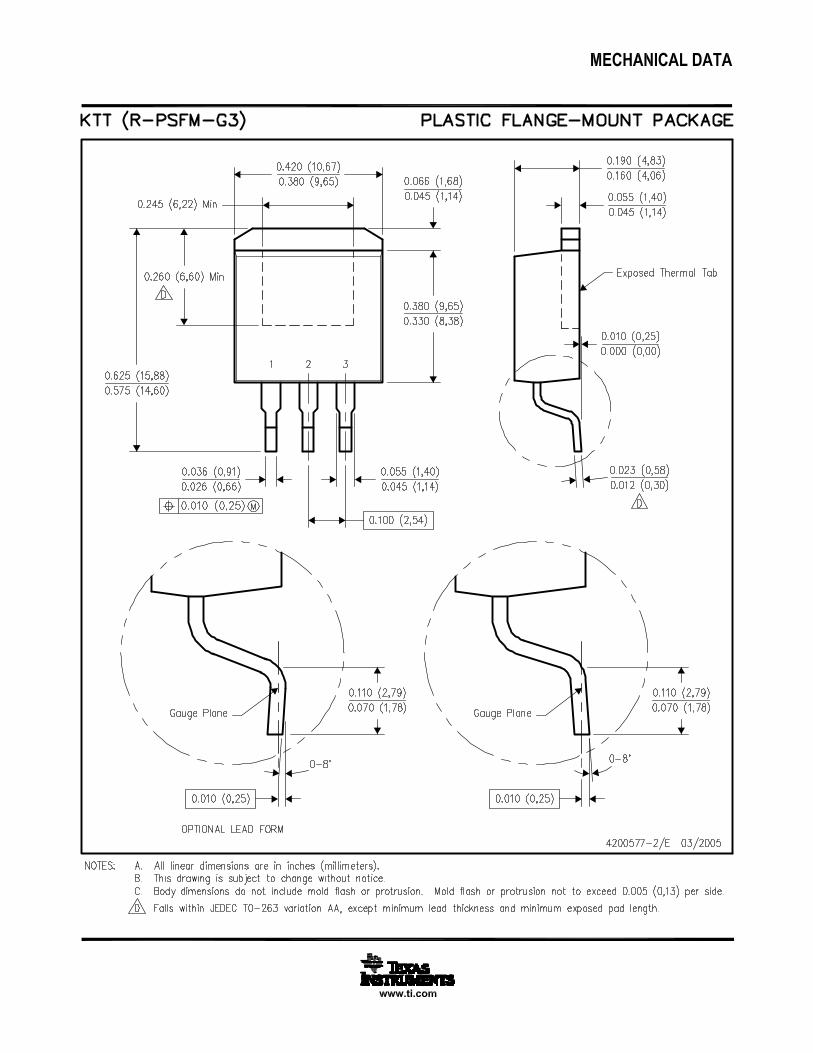
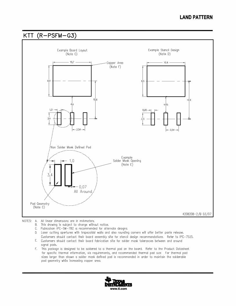
LM337...KTT (TO-263) PACKAGE
(TOP VIEW)
OUTPUT
INPUT
ADJUSTMENT
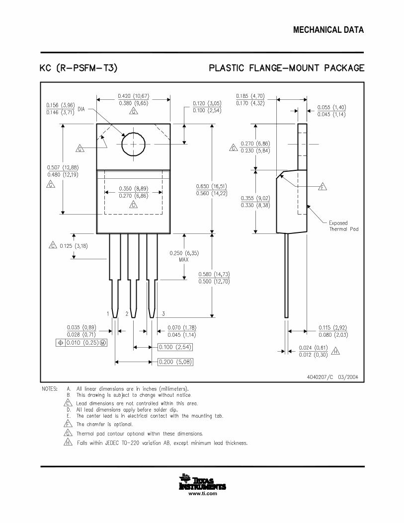
LM237, LM337...KC (TO-220) PACKAGE
(TOP VIEW)
INPUTOUTPUT
ADJUSTMENT
INPUTOUTPUT
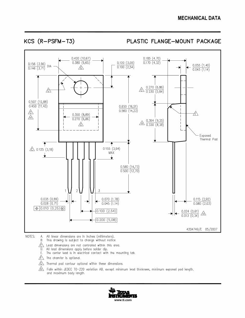
LM337...KCS (TO-220) PACKAGE
(TOP VIEW)
ADJUSTMENTINP
UT
INP
UT
DESCRIPTION/ORDERING INFORMATION
LM237, LM3373-TERMINAL ADJUSTABLE REGULATORS
SLVS047K–NOVEMBER 1981–REVISED NOVEMBER 2007www.ti.com
2• Output Voltage Range Adjustable From • Peak Output Current Constant Over–1.2 V to –37 V Temperature Range of Regulator
• Output Current Capability of 1.5 A Max • Ripple Rejection Typically 77 dB• Input Regulation Typically 0.01% Per • Direct Replacement for Industry-Standard
Input-Voltage Change LM237 and LM337• Output Regulation Typically 0.3%
The LM237 and LM337 are adjustable 3-terminal negative-voltage regulators capable of supplying in excess of–1.5 A over an output voltage range of –1.2 V to –37 V. They are exceptionally easy to use, requiring only twoexternal resistors to set the output voltage and one output capacitor for frequency compensation. The currentdesign has been optimized for excellent regulation and low thermal transients. In addition, the LM237 and LM337feature internal current limiting, thermal shutdown, and safe-area compensation, making them virtually immune tofailure by overloads.
The LM237 and LM337 serve a wide variety of applications, including local on-card regulation, programmableoutput-voltage regulation, and precision current regulation.
ORDERING INFORMATIONTJ PACKAGE (1) ORDERABLE PART NUMBER TOP-SIDE MARKING
–25°C to 150°C TO-220 – KC Tube of 50 LM237KC LM237PowerFLEX™ – KTE Reel of 2000 LM337KTER LM337PowerFLEX – KTP Reel of 3000 LM337KTPR L337TO-220 – KC Tube of 50 LM337KC LM337
0°C to 125°CTO-220 – KCS Tube of 50 LM337KCSE3 LM337TO-252 – KVU Reel of 2500 LM337KVURG3 LM337TO-263 – KTT Reel of 500 LM337KTTR LM337
(1) Package drawings, standard packing quantities, thermal data, symbolization, and PCB design guidelines are available atwww.ti.com/sc/package.
1
Please be aware that an important notice concerning availability, standard warranty, and use in critical applications ofTexas Instruments semiconductor products and disclaimers thereto appears at the end of this data sheet.
2PowerFLEX is a trademark of Texas Instruments.
PRODUCTION DATA information is current as of publication date. Copyright © 1981–2007, Texas Instruments IncorporatedProducts conform to specifications per the terms of the TexasInstruments standard warranty. Production processing does notnecessarily include testing of all parameters.
www.ti.com
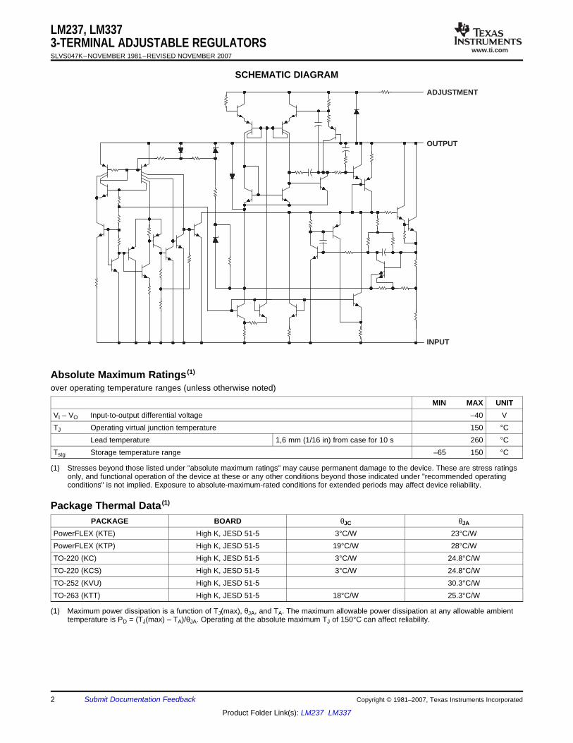
ADJUSTMENT
OUTPUT
INPUT
Absolute Maximum Ratings (1)
Package Thermal Data (1)
LM237, LM3373-TERMINAL ADJUSTABLE REGULATORSSLVS047K–NOVEMBER 1981–REVISED NOVEMBER 2007
SCHEMATIC DIAGRAM
over operating temperature ranges (unless otherwise noted)
MIN MAX UNITVI – VO Input-to-output differential voltage –40 VTJ Operating virtual junction temperature 150 °C
Lead temperature 1,6 mm (1/16 in) from case for 10 s 260 °CTstg Storage temperature range –65 150 °C
(1) Stresses beyond those listed under "absolute maximum ratings" may cause permanent damage to the device. These are stress ratingsonly, and functional operation of the device at these or any other conditions beyond those indicated under "recommended operatingconditions" is not implied. Exposure to absolute-maximum-rated conditions for extended periods may affect device reliability.
PACKAGE BOARD θJC θJA
PowerFLEX (KTE) High K, JESD 51-5 3°C/W 23°C/WPowerFLEX (KTP) High K, JESD 51-5 19°C/W 28°C/WTO-220 (KC) High K, JESD 51-5 3°C/W 24.8°C/WTO-220 (KCS) High K, JESD 51-5 3°C/W 24.8°C/WTO-252 (KVU) High K, JESD 51-5 30.3°C/WTO-263 (KTT) High K, JESD 51-5 18°C/W 25.3°C/W
(1) Maximum power dissipation is a function of TJ(max), θJA, and TA. The maximum allowable power dissipation at any allowable ambienttemperature is PD = (TJ(max) – TA)/θJA. Operating at the absolute maximum TJ of 150°C can affect reliability.
2 Submit Documentation Feedback Copyright © 1981–2007, Texas Instruments Incorporated
Product Folder Link(s): LM237 LM337
www.ti.com
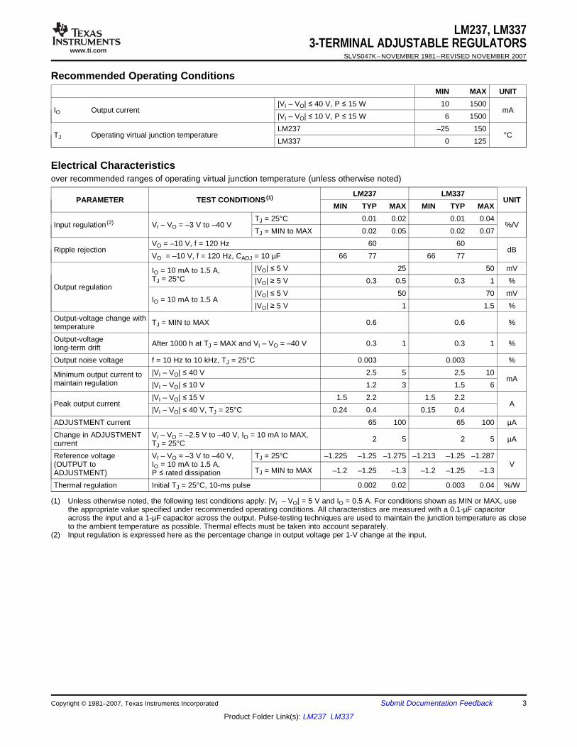
Recommended Operating Conditions
Electrical Characteristics
LM237, LM3373-TERMINAL ADJUSTABLE REGULATORS
SLVS047K–NOVEMBER 1981–REVISED NOVEMBER 2007
MIN MAX UNIT|VI – VO| ≤ 40 V, P ≤ 15 W 10 1500
IO Output current mA|VI – VO| ≤ 10 V, P ≤ 15 W 6 1500LM237 –25 150
TJ Operating virtual junction temperature °CLM337 0 125
over recommended ranges of operating virtual junction temperature (unless otherwise noted)
LM237 LM337PARAMETER TEST CONDITIONS (1) UNIT
MIN TYP MAX MIN TYP MAXTJ = 25°C 0.01 0.02 0.01 0.04
Input regulation (2) VI – VO = –3 V to –40 V %/VTJ = MIN to MAX 0.02 0.05 0.02 0.07
VO = –10 V, f = 120 Hz 60 60Ripple rejection dB
VO = –10 V, f = 120 Hz, CADJ = 10 µF 66 77 66 77|VO| ≤ 5 V 25 50 mVIO = 10 mA to 1.5 A,
TJ = 25°C |VO| ≥ 5 V 0.3 0.5 0.3 1 %Output regulation
|VO| ≤ 5 V 50 70 mVIO = 10 mA to 1.5 A
|VO| ≥ 5 V 1 1.5 %Output-voltage change with TJ = MIN to MAX 0.6 0.6 %temperatureOutput-voltage After 1000 h at TJ = MAX and VI – VO = –40 V 0.3 1 0.3 1 %long-term driftOutput noise voltage f = 10 Hz to 10 kHz, TJ = 25°C 0.003 0.003 %
|VI – VO| ≤ 40 V 2.5 5 2.5 10Minimum output current to mAmaintain regulation |VI – VO| ≤ 10 V 1.2 3 1.5 6|VI – VO| ≤ 15 V 1.5 2.2 1.5 2.2
Peak output current A|VI – VO| ≤ 40 V, TJ = 25°C 0.24 0.4 0.15 0.4
ADJUSTMENT current 65 100 65 100 µAChange in ADJUSTMENT VI – VO = –2.5 V to –40 V, IO = 10 mA to MAX, 2 5 2 5 µAcurrent TJ = 25°CReference voltage VI – VO = –3 V to –40 V, TJ = 25°C –1.225 –1.25 –1.275 –1.213 –1.25 –1.287(OUTPUT to IO = 10 mA to 1.5 A, V
TJ = MIN to MAX –1.2 –1.25 –1.3 –1.2 –1.25 –1.3ADJUSTMENT) P ≤ rated dissipationThermal regulation Initial TJ = 25°C, 10-ms pulse 0.002 0.02 0.003 0.04 %/W
(1) Unless otherwise noted, the following test conditions apply: |VI – VO| = 5 V and IO = 0.5 A. For conditions shown as MIN or MAX, usethe appropriate value specified under recommended operating conditions. All characteristics are measured with a 0.1-µF capacitoracross the input and a 1-µF capacitor across the output. Pulse-testing techniques are used to maintain the junction temperature as closeto the ambient temperature as possible. Thermal effects must be taken into account separately.
(2) Input regulation is expressed here as the percentage change in output voltage per 1-V change at the input.
Copyright © 1981–2007, Texas Instruments Incorporated Submit Documentation Feedback 3
Product Folder Link(s): LM237 LM337
www.ti.com
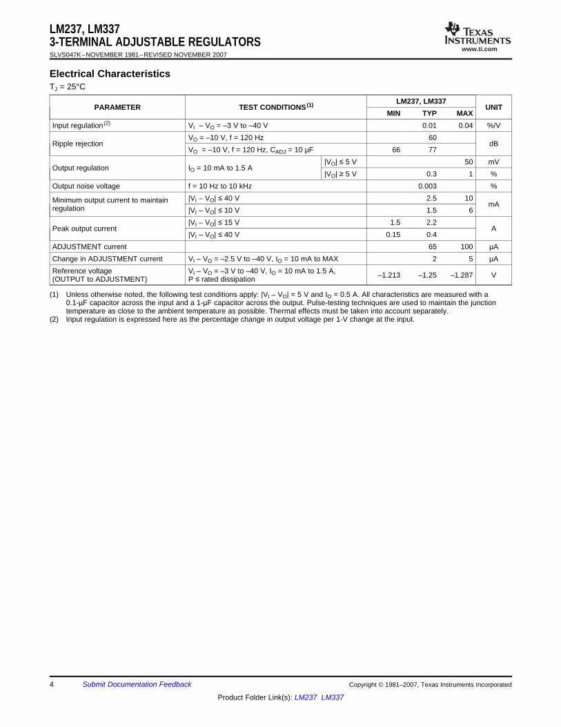
Electrical Characteristics
LM237, LM3373-TERMINAL ADJUSTABLE REGULATORSSLVS047K–NOVEMBER 1981–REVISED NOVEMBER 2007
TJ = 25°C
LM237, LM337PARAMETER TEST CONDITIONS (1) UNIT
MIN TYP MAXInput regulation (2) VI – VO = –3 V to –40 V 0.01 0.04 %/V
VO = –10 V, f = 120 Hz 60Ripple rejection dB
VO = –10 V, f = 120 Hz, CADJ = 10 µF 66 77|VO| ≤ 5 V 50 mV
Output regulation IO = 10 mA to 1.5 A|VO| ≥ 5 V 0.3 1 %
Output noise voltage f = 10 Hz to 10 kHz 0.003 %|VI – VO| ≤ 40 V 2.5 10Minimum output current to maintain mAregulation |VI – VO| ≤ 10 V 1.5 6|VI – VO| ≤ 15 V 1.5 2.2
Peak output current A|VI – VO| ≤ 40 V 0.15 0.4
ADJUSTMENT current 65 100 µAChange in ADJUSTMENT current VI – VO = –2.5 V to –40 V, IO = 10 mA to MAX 2 5 µAReference voltage VI – VO = –3 V to –40 V, IO = 10 mA to 1.5 A, –1.213 –1.25 –1.287 V(OUTPUT to ADJUSTMENT) P ≤ rated dissipation
(1) Unless otherwise noted, the following test conditions apply: |VI – VO| = 5 V and IO = 0.5 A. All characteristics are measured with a0.1-µF capacitor across the input and a 1-µF capacitor across the output. Pulse-testing techniques are used to maintain the junctiontemperature as close to the ambient temperature as possible. Thermal effects must be taken into account separately.
(2) Input regulation is expressed here as the percentage change in output voltage per 1-V change at the input.
4 Submit Documentation Feedback Copyright © 1981–2007, Texas Instruments Incorporated
Product Folder Link(s): LM237 LM337
www.ti.com
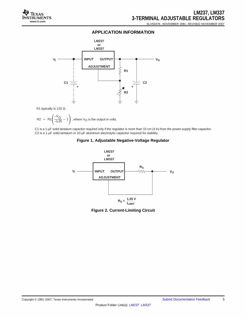
APPLICATION INFORMATION
C1+
C2
R1
R2
+
INPUT OUTPUT
ADJUSTMENT
LM237or
LM337
VOVI
C1 is a 1-µF solid tantalum capacitor required only if the regulator is more than 10 cm (4 in) from the power-supply filter capacitor.C2 is a 1-µF solid tantalum or 10-µF aluminum electrolytic capacitor required for stability.
R2 R1–VO–1..25
1R1 typically is 120 Ω.
, where VO is the output in volts.
ADJUSTMENT
OUTPUTINPUTVI
RS
VO
LM237or
LM337
RS = 1.25 VILIMIT
LM237, LM3373-TERMINAL ADJUSTABLE REGULATORS
SLVS047K–NOVEMBER 1981–REVISED NOVEMBER 2007
Figure 1. Adjustable Negative-Voltage Regulator
Figure 2. Current-Limiting Circuit
Copyright © 1981–2007, Texas Instruments Incorporated Submit Documentation Feedback 5
Product Folder Link(s): LM237 LM337
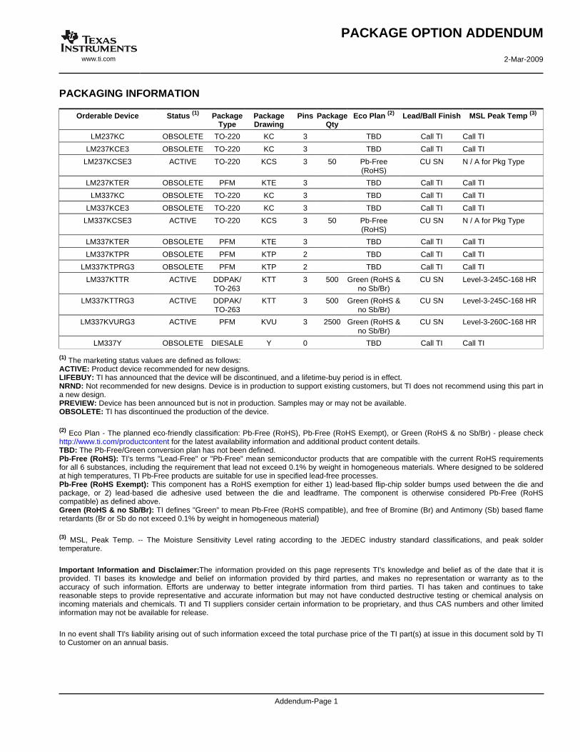
PACKAGING INFORMATION
Orderable Device Status (1) PackageType
PackageDrawing
Pins PackageQty
Eco Plan (2) Lead/Ball Finish MSL Peak Temp (3)
LM237KC OBSOLETE TO-220 KC 3 TBD Call TI Call TI
LM237KCE3 OBSOLETE TO-220 KC 3 TBD Call TI Call TI
LM237KCSE3 ACTIVE TO-220 KCS 3 50 Pb-Free(RoHS)
CU SN N / A for Pkg Type
LM237KTER OBSOLETE PFM KTE 3 TBD Call TI Call TI
LM337KC OBSOLETE TO-220 KC 3 TBD Call TI Call TI
LM337KCE3 OBSOLETE TO-220 KC 3 TBD Call TI Call TI
LM337KCSE3 ACTIVE TO-220 KCS 3 50 Pb-Free(RoHS)
CU SN N / A for Pkg Type
LM337KTER OBSOLETE PFM KTE 3 TBD Call TI Call TI
LM337KTPR OBSOLETE PFM KTP 2 TBD Call TI Call TI
LM337KTPRG3 OBSOLETE PFM KTP 2 TBD Call TI Call TI
LM337KTTR ACTIVE DDPAK/TO-263
KTT 3 500 Green (RoHS &no Sb/Br)
CU SN Level-3-245C-168 HR
LM337KTTRG3 ACTIVE DDPAK/TO-263
KTT 3 500 Green (RoHS &no Sb/Br)
CU SN Level-3-245C-168 HR
LM337KVURG3 ACTIVE PFM KVU 3 2500 Green (RoHS &no Sb/Br)
CU SN Level-3-260C-168 HR
LM337Y OBSOLETE DIESALE Y 0 TBD Call TI Call TI
(1) The marketing status values are defined as follows:ACTIVE: Product device recommended for new designs.LIFEBUY: TI has announced that the device will be discontinued, and a lifetime-buy period is in effect.NRND: Not recommended for new designs. Device is in production to support existing customers, but TI does not recommend using this part ina new design.PREVIEW: Device has been announced but is not in production. Samples may or may not be available.OBSOLETE: TI has discontinued the production of the device.
(2) Eco Plan - The planned eco-friendly classification: Pb-Free (RoHS), Pb-Free (RoHS Exempt), or Green (RoHS & no Sb/Br) - please checkhttp://www.ti.com/productcontent for the latest availability information and additional product content details.TBD: The Pb-Free/Green conversion plan has not been defined.Pb-Free (RoHS): TI's terms "Lead-Free" or "Pb-Free" mean semiconductor products that are compatible with the current RoHS requirementsfor all 6 substances, including the requirement that lead not exceed 0.1% by weight in homogeneous materials. Where designed to be solderedat high temperatures, TI Pb-Free products are suitable for use in specified lead-free processes.Pb-Free (RoHS Exempt): This component has a RoHS exemption for either 1) lead-based flip-chip solder bumps used between the die andpackage, or 2) lead-based die adhesive used between the die and leadframe. The component is otherwise considered Pb-Free (RoHScompatible) as defined above.Green (RoHS & no Sb/Br): TI defines "Green" to mean Pb-Free (RoHS compatible), and free of Bromine (Br) and Antimony (Sb) based flameretardants (Br or Sb do not exceed 0.1% by weight in homogeneous material)
(3) MSL, Peak Temp. -- The Moisture Sensitivity Level rating according to the JEDEC industry standard classifications, and peak soldertemperature.
Important Information and Disclaimer:The information provided on this page represents TI's knowledge and belief as of the date that it isprovided. TI bases its knowledge and belief on information provided by third parties, and makes no representation or warranty as to theaccuracy of such information. Efforts are underway to better integrate information from third parties. TI has taken and continues to takereasonable steps to provide representative and accurate information but may not have conducted destructive testing or chemical analysis onincoming materials and chemicals. TI and TI suppliers consider certain information to be proprietary, and thus CAS numbers and other limitedinformation may not be available for release.
In no event shall TI's liability arising out of such information exceed the total purchase price of the TI part(s) at issue in this document sold by TIto Customer on an annual basis.
PACKAGE OPTION ADDENDUM
www.ti.com 2-Mar-2009
Addendum-Page 1
PACKAGE OPTION ADDENDUM
www.ti.com 2-Mar-2009
Addendum-Page 2
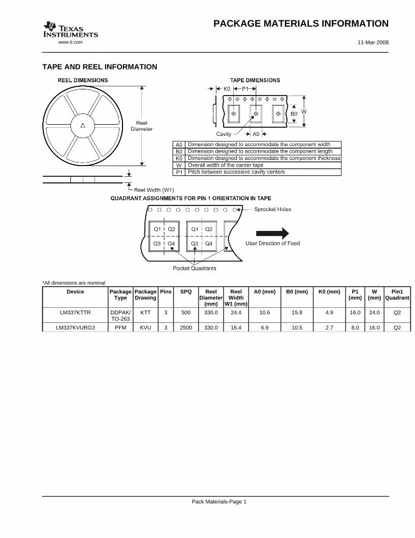
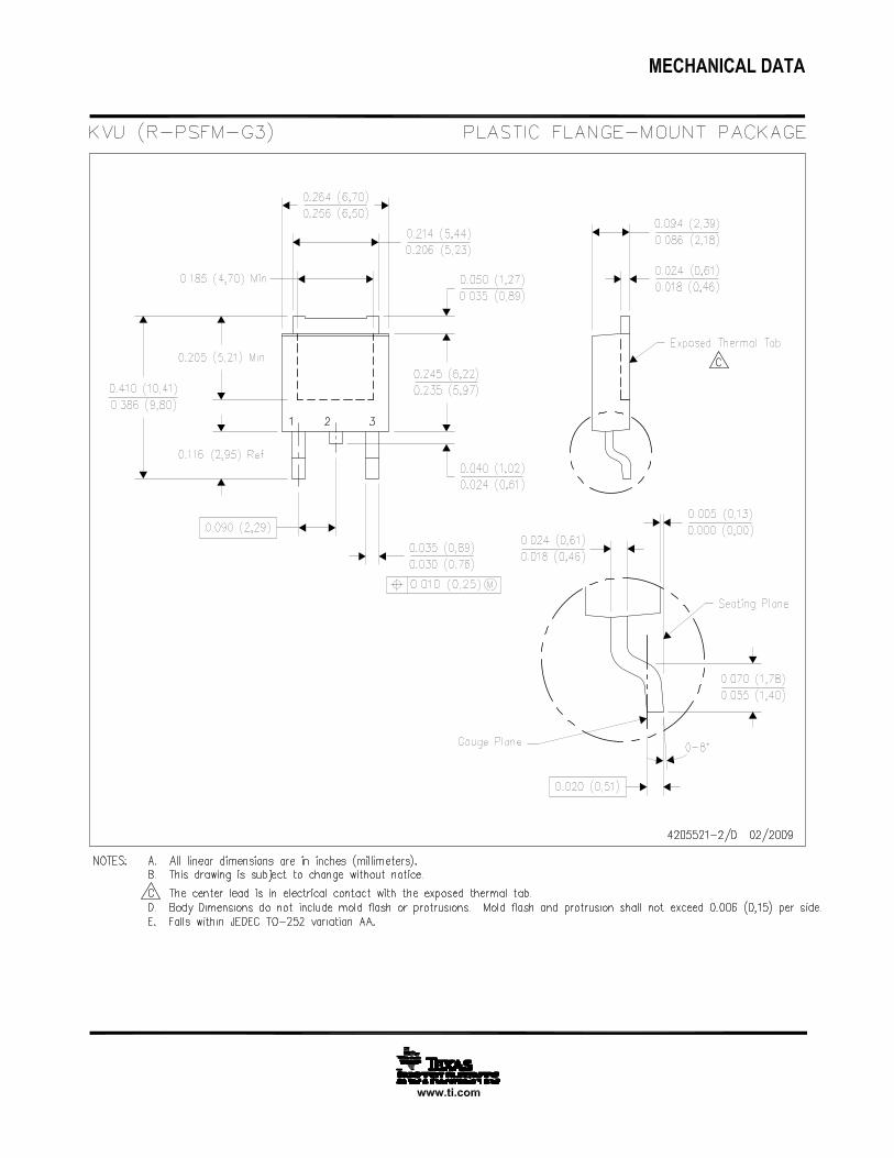
TAPE AND REEL INFORMATION
*All dimensions are nominal
Device PackageType
PackageDrawing
Pins SPQ ReelDiameter
(mm)
ReelWidth
W1 (mm)
A0 (mm) B0 (mm) K0 (mm) P1(mm)
W(mm)
Pin1Quadrant
LM337KTTR DDPAK/TO-263
KTT 3 500 330.0 24.4 10.6 15.8 4.9 16.0 24.0 Q2
LM337KVURG3 PFM KVU 3 2500 330.0 16.4 6.9 10.5 2.7 8.0 16.0 Q2
PACKAGE MATERIALS INFORMATION
www.ti.com 11-Mar-2008
Pack Materials-Page 1
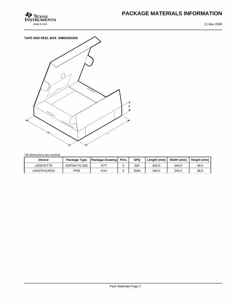
*All dimensions are nominal
Device Package Type Package Drawing Pins SPQ Length (mm) Width (mm) Height (mm)
LM337KTTR DDPAK/TO-263 KTT 3 500 340.0 340.0 38.0
LM337KVURG3 PFM KVU 3 2500 340.0 340.0 38.0
PACKAGE MATERIALS INFORMATION
www.ti.com 11-Mar-2008
Pack Materials-Page 2
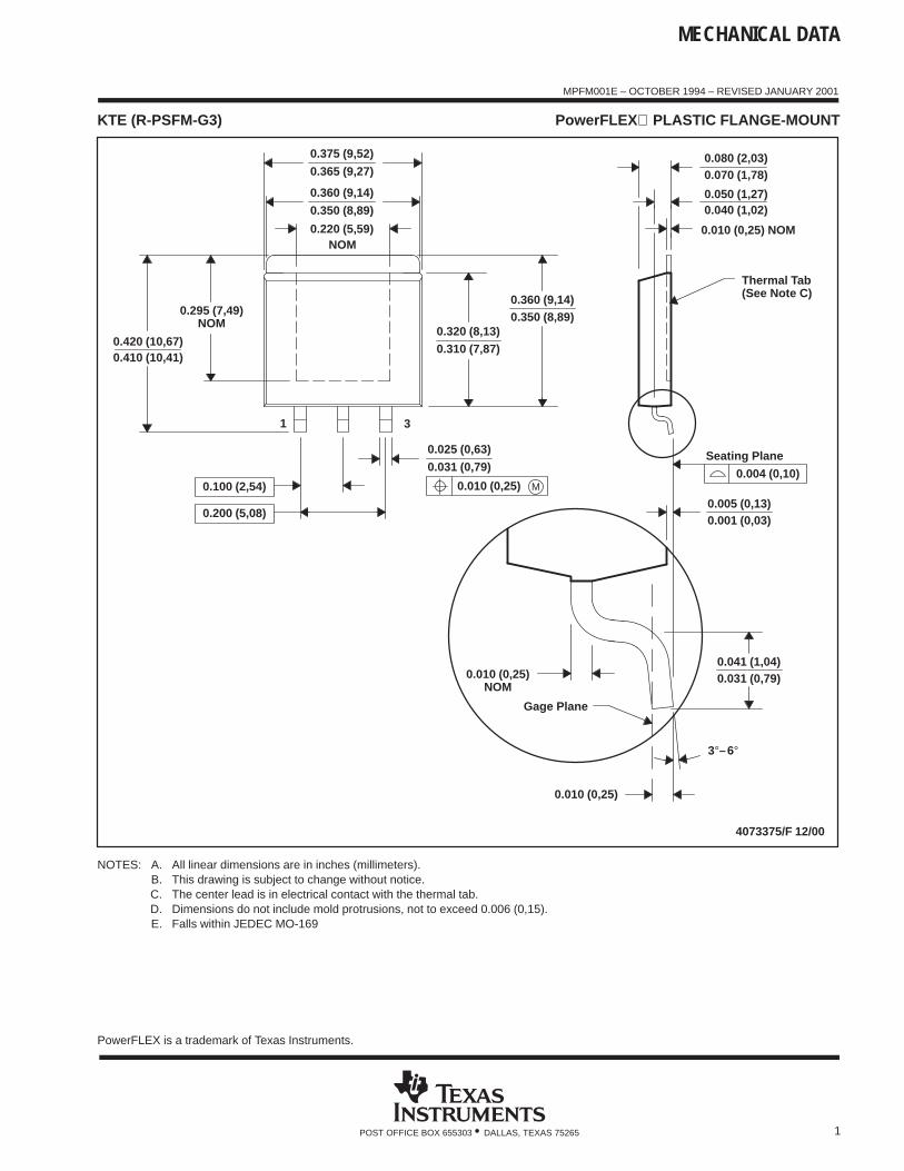
MECHANICAL DATA
MPFM001E – OCTOBER 1994 – REVISED JANUARY 2001
1POST OFFICE BOX 655303 • DALLAS, TEXAS 75265
KTE (R-PSFM-G3) PowerFLEX PLASTIC FLANGE-MOUNT
0.360 (9,14)0.350 (8,89)
0.080 (2,03)0.070 (1,78)
0.010 (0,25) NOM
0.040 (1,02)
Seating Plane
0.050 (1,27)
0.001 (0,03)0.005 (0,13)
0.010 (0,25)NOM
Gage Plane
0.010 (0,25)
0.031 (0,79)0.041 (1,04)
4073375/F 12/00
NOM
31
0.350 (8,89)
0.220 (5,59)
0.360 (9,14)
0.295 (7,49)NOM
0.320 (8,13)0.310 (7,87)
0.025 (0,63)
0.031 (0,79)
Thermal Tab(See Note C)
0.004 (0,10)M0.010 (0,25)0.100 (2,54)
3°–6°
0.410 (10,41)0.420 (10,67)
0.200 (5,08)
0.365 (9,27)
0.375 (9,52)
NOTES: A. All linear dimensions are in inches (millimeters).B. This drawing is subject to change without notice.C. The center lead is in electrical contact with the thermal tab.D. Dimensions do not include mold protrusions, not to exceed 0.006 (0,15).E. Falls within JEDEC MO-169
PowerFLEX is a trademark of Texas Instruments.
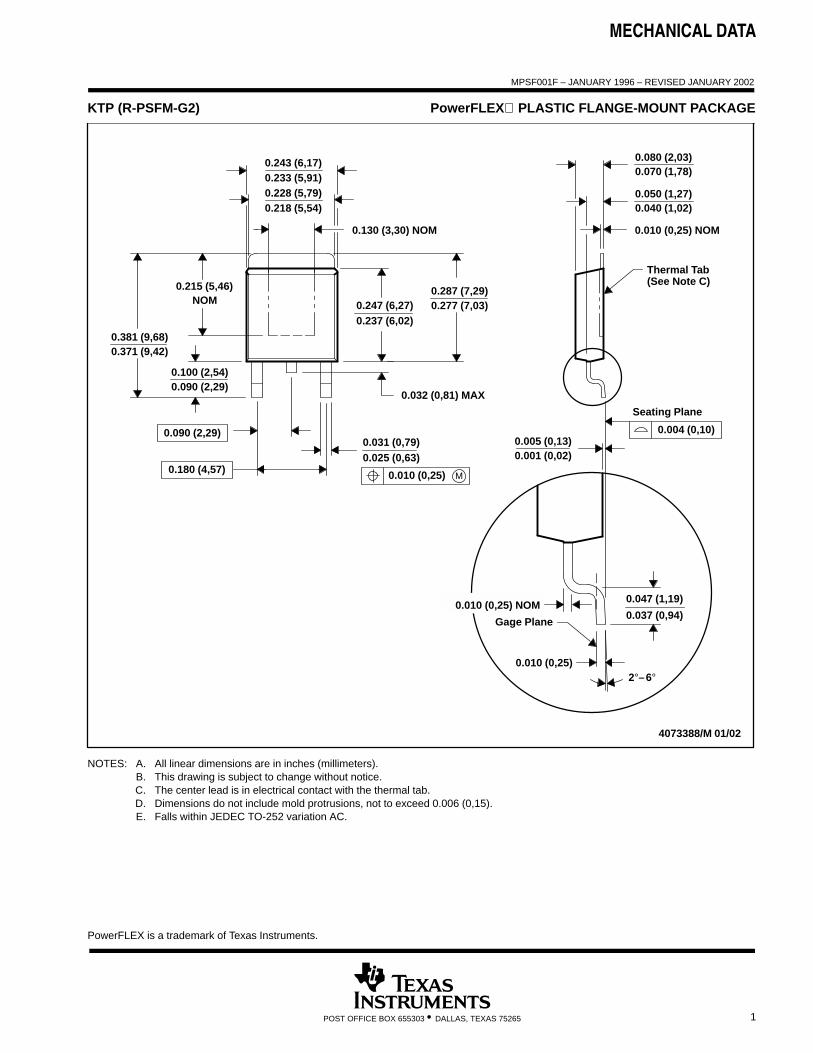
MECHANICAL DATA
MPSF001F – JANUARY 1996 – REVISED JANUARY 2002
1POST OFFICE BOX 655303 • DALLAS, TEXAS 75265
KTP (R-PSFM-G2) PowerFLEX PLASTIC FLANGE-MOUNT PACKAGE
0.228 (5,79)0.218 (5,54)
0.233 (5,91)0.243 (6,17)
0.001 (0,02)0.005 (0,13)
0.070 (1,78)
Seating Plane
0.080 (2,03)
0.010 (0,25) NOM
Gage Plane
0.010 (0,25)
4073388/M 01/02
0.037 (0,94)
0.047 (1,19)
0.247 (6,27)0.237 (6,02)
NOM0.215 (5,46)
0.371 (9,42)0.381 (9,68)
0.090 (2,29)0.100 (2,54)
0.287 (7,29)
0.031 (0,79)
0.032 (0,81) MAX
0.277 (7,03)
0.025 (0,63)
0.130 (3,30) NOM
0.090 (2,29)
0.180 (4,57)M0.010 (0,25)
0.004 (0,10)
2°–6°
0.040 (1,02)0.050 (1,27)
Thermal Tab(See Note C)
0.010 (0,25) NOM
NOTES: A. All linear dimensions are in inches (millimeters).B. This drawing is subject to change without notice.C. The center lead is in electrical contact with the thermal tab.D. Dimensions do not include mold protrusions, not to exceed 0.006 (0,15).E. Falls within JEDEC TO-252 variation AC.
PowerFLEX is a trademark of Texas Instruments.
IMPORTANT NOTICETexas Instruments Incorporated and its subsidiaries (TI) reserve the right to make corrections, modifications, enhancements, improvements,and other changes to its products and services at any time and to discontinue any product or service without notice. Customers shouldobtain the latest relevant information before placing orders and should verify that such information is current and complete. All products aresold subject to TI’s terms and conditions of sale supplied at the time of order acknowledgment.TI warrants performance of its hardware products to the specifications applicable at the time of sale in accordance with TI’s standardwarranty. Testing and other quality control techniques are used to the extent TI deems necessary to support this warranty. Except wheremandated by government requirements, testing of all parameters of each product is not necessarily performed.TI assumes no liability for applications assistance or customer product design. Customers are responsible for their products andapplications using TI components. To minimize the risks associated with customer products and applications, customers should provideadequate design and operating safeguards.TI does not warrant or represent that any license, either express or implied, is granted under any TI patent right, copyright, mask work right,or other TI intellectual property right relating to any combination, machine, or process in which TI products or services are used. Informationpublished by TI regarding third-party products or services does not constitute a license from TI to use such products or services or awarranty or endorsement thereof. Use of such information may require a license from a third party under the patents or other intellectualproperty of the third party, or a license from TI under the patents or other intellectual property of TI.Reproduction of TI information in TI data books or data sheets is permissible only if reproduction is without alteration and is accompaniedby all associated warranties, conditions, limitations, and notices. Reproduction of this information with alteration is an unfair and deceptivebusiness practice. TI is not responsible or liable for such altered documentation. Information of third parties may be subject to additionalrestrictions.Resale of TI products or services with statements different from or beyond the parameters stated by TI for that product or service voids allexpress and any implied warranties for the associated TI product or service and is an unfair and deceptive business practice. TI is notresponsible or liable for any such statements.TI products are not authorized for use in safety-critical applications (such as life support) where a failure of the TI product would reasonablybe expected to cause severe personal injury or death, unless officers of the parties have executed an agreement specifically governingsuch use. Buyers represent that they have all necessary expertise in the safety and regulatory ramifications of their applications, andacknowledge and agree that they are solely responsible for all legal, regulatory and safety-related requirements concerning their productsand any use of TI products in such safety-critical applications, notwithstanding any applications-related information or support that may beprovided by TI. Further, Buyers must fully indemnify TI and its representatives against any damages arising out of the use of TI products insuch safety-critical applications.TI products are neither designed nor intended for use in military/aerospace applications or environments unless the TI products arespecifically designated by TI as military-grade or "enhanced plastic." Only products designated by TI as military-grade meet militaryspecifications. Buyers acknowledge and agree that any such use of TI products which TI has not designated as military-grade is solely atthe Buyer's risk, and that they are solely responsible for compliance with all legal and regulatory requirements in connection with such use.TI products are neither designed nor intended for use in automotive applications or environments unless the specific TI products aredesignated by TI as compliant with ISO/TS 16949 requirements. Buyers acknowledge and agree that, if they use any non-designatedproducts in automotive applications, TI will not be responsible for any failure to meet such requirements.Following are URLs where you can obtain information on other Texas Instruments products and application solutions:Products ApplicationsAmplifiers amplifier.ti.com Audio www.ti.com/audioData Converters dataconverter.ti.com Automotive www.ti.com/automotiveDLP® Products www.dlp.com Broadband www.ti.com/broadbandDSP dsp.ti.com Digital Control www.ti.com/digitalcontrolClocks and Timers www.ti.com/clocks Medical www.ti.com/medicalInterface interface.ti.com Military www.ti.com/militaryLogic logic.ti.com Optical Networking www.ti.com/opticalnetworkPower Mgmt power.ti.com Security www.ti.com/securityMicrocontrollers microcontroller.ti.com Telephony www.ti.com/telephonyRFID www.ti-rfid.com Video & Imaging www.ti.com/videoRF/IF and ZigBee® Solutions www.ti.com/lprf Wireless www.ti.com/wireless
Mailing Address: Texas Instruments, Post Office Box 655303, Dallas, Texas 75265Copyright © 2009, Texas Instruments Incorporated